EP3358830A1 - Imaging element, imaging device, and electronic apparatus - Google Patents
Imaging element, imaging device, and electronic apparatus Download PDFInfo
- Publication number
- EP3358830A1 EP3358830A1 EP16851552.6A EP16851552A EP3358830A1 EP 3358830 A1 EP3358830 A1 EP 3358830A1 EP 16851552 A EP16851552 A EP 16851552A EP 3358830 A1 EP3358830 A1 EP 3358830A1
- Authority
- EP
- European Patent Office
- Prior art keywords
- electric current
- circuit
- signal
- current source
- analog
- Prior art date
- Legal status (The legal status is an assumption and is not a legal conclusion. Google has not performed a legal analysis and makes no representation as to the accuracy of the status listed.)
- Granted
Links
- 238000003384 imaging method Methods 0.000 title 2
- 238000006243 chemical reaction Methods 0.000 claims abstract description 59
- 239000003990 capacitor Substances 0.000 description 67
- 230000015654 memory Effects 0.000 description 45
- 238000010586 diagram Methods 0.000 description 13
- 238000009792 diffusion process Methods 0.000 description 11
- 238000000034 method Methods 0.000 description 7
- 230000003321 amplification Effects 0.000 description 5
- 238000003199 nucleic acid amplification method Methods 0.000 description 5
- 230000006870 function Effects 0.000 description 3
- 230000007423 decrease Effects 0.000 description 1
- 239000004065 semiconductor Substances 0.000 description 1
Images


Classifications
-
- H—ELECTRICITY
- H04—ELECTRIC COMMUNICATION TECHNIQUE
- H04N—PICTORIAL COMMUNICATION, e.g. TELEVISION
- H04N25/00—Circuitry of solid-state image sensors [SSIS]; Control thereof
- H04N25/70—SSIS architectures; Circuits associated therewith
- H04N25/71—Charge-coupled device [CCD] sensors; Charge-transfer registers specially adapted for CCD sensors
- H04N25/75—Circuitry for providing, modifying or processing image signals from the pixel array
-
- H—ELECTRICITY
- H03—ELECTRONIC CIRCUITRY
- H03M—CODING; DECODING; CODE CONVERSION IN GENERAL
- H03M1/00—Analogue/digital conversion; Digital/analogue conversion
- H03M1/12—Analogue/digital converters
- H03M1/50—Analogue/digital converters with intermediate conversion to time interval
- H03M1/56—Input signal compared with linear ramp
-
- H—ELECTRICITY
- H04—ELECTRIC COMMUNICATION TECHNIQUE
- H04N—PICTORIAL COMMUNICATION, e.g. TELEVISION
- H04N25/00—Circuitry of solid-state image sensors [SSIS]; Control thereof
- H04N25/70—SSIS architectures; Circuits associated therewith
- H04N25/709—Circuitry for control of the power supply
-
- H—ELECTRICITY
- H04—ELECTRIC COMMUNICATION TECHNIQUE
- H04N—PICTORIAL COMMUNICATION, e.g. TELEVISION
- H04N25/00—Circuitry of solid-state image sensors [SSIS]; Control thereof
- H04N25/70—SSIS architectures; Circuits associated therewith
- H04N25/76—Addressed sensors, e.g. MOS or CMOS sensors
- H04N25/77—Pixel circuitry, e.g. memories, A/D converters, pixel amplifiers, shared circuits or shared components
- H04N25/772—Pixel circuitry, e.g. memories, A/D converters, pixel amplifiers, shared circuits or shared components comprising A/D, V/T, V/F, I/T or I/F converters
Abstract
Description
- The present invention relates to an image sensor, an image-capturing apparatus, and an electronic device.
- Pixel circuits are provided with load transistors that serves as electric current sources (PTL1). Generally, the pixel circuit is provided with an electric current source circuit including a capacitor and an electric current source for supplying an electric current source with a bias voltage, and a reference electric current is inputted to the capacitor of the electric current source circuit from an external reference electric current source. In order to hold the bias voltage of the capacitor, it is required to supply the reference electric current from the external reference electric current source. Additionally, as the number of pixel circuits increases, the required number of electric current source circuits increases accordingly. This leads to an increased reference electric current supplied from the external reference electric current source and thus an increased power consumption.
- PTL1: Japanese Laid-Open Patent Publication No.
2006-49361 - According to the 1st aspect, an image sensor comprises: a readout circuit that reads out a signal to a signal line, the signal being generated by an electric charge resulting from a photoelectric conversion; a storage circuit including an analog/digital converter that converts a first voltage signal based on an electric current from a first power supply circuit into a digital signal and a first storage unit that stores the first voltage signal converted into a digital signal by the analog/digital converter; and a first electric current source that supplies the signal line with an electric current generated by the first voltage signal stored in the first storage unit.
- According to the 2nd aspect, an electronic device comprises: an electronic circuit having a plurality of electronic components; a storage circuit including an analog/digital converter that converts a first voltage signal based on an electric current from a first power supply circuit into a digital signal, and a first storage unit that stores the first voltage signal converted into the digital signal by the analog/digital converter; and a first electric current source that supplies the electronic circuit with an electric current generated by the first voltage signal stored in the first storage unit.
-
- [
Fig. 1] Figs. 1(A) and 1(B) illustrate an electric current source circuit and a time sequence diagram according to a first embodiment. - [
Fig. 2] Fig. 2 is a circuit configuration diagram of a pixel circuit. - [
Fig. 3 ]Figs. 3(A) ,3(B) , and3(C) illustrates an electric current source circuit according to a variation of the first embodiment. - [
Fig. 4] Fig. 4 illustrates an electric current source circuit according to a second embodiment. - [
Fig. 5] Fig. 5 illustrates an electric current source circuit according to a third embodiment. - [
Fig. 6] Fig. 6 is a time sequence diagram of an electric current source circuit according to the third embodiment. - [
Fig. 7] Fig. 7 illustrates a pixel chip according to a fourth embodiment. - [
Fig. 8] Fig. 8 illustrates a second electric current source circuit according to the fourth embodiment. - [
Fig. 9] Fig. 9 is a time sequence diagram of the pixel chip according to the fourth embodiment. -
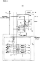
Fig. 1(A) is a configuration diagram of an electric current source circuit according to a first embodiment. - A
storage circuit 111 has a storage unit including a capacitor Cb, an A/D converter 13, amemory 14, and a D/A converter 15, and a control unit including switches SW10 to SW14. Thestorage circuit 111 stores a voltage based on a reference electric current Ic outputted from a reference electric current source in the storage unit. Thestorage circuit 111 is connected to a gate terminal of an electriccurrent source 112 composed of a MOS transistor Tr1 and supplies the stored voltage to the electriccurrent source 112. - The electric
current source 112 supplies acircuit 12 with an electric current based on the voltage stored in the storage unit. The storage unit has at least a capacitive element such as a capacitor having one electrode connected to a gate terminal of the MOS transistor Tr1 and the other electrode connected to a node having the same potential as that of a source terminal, for example. - The reference electric current Ic is inputted to the electric
current source circuit 11 from a terminal P1. The reference electric current Ic is inputted to a drain of the MOS transistor Tr1 when the switch SW10 is turned off and the switches SW11 and SW12 are turned on. One end of the capacitor Cb is connected to a gate side of the MOS transistor Tr1 and the other end of the capacitor Cb is connected to a predetermined voltage terminal having the same potential as that of the source terminal of the MOS transistor Tr1. A drain side of the MOS transistor Tr1 is connected to thecircuit 12 via the switch SW10. Furthermore, the drain side of the MOS transistor Tr1 is connected to the gate terminal and one end of the capacitor Cb via the switch SW12 so as to constitute a so-called diode connection and generate a bias voltage Vb. When the switches SW11 and SW12 are turned off and the switch SW10 is turned on, the MOS transistor Tr1 serving as the electriccurrent source 112 generates a constant electric current Ic based on the bias voltage Vb and supplies the constant electric current Ic to thecircuit 12. An example of thecircuit 12 is a pixel circuit as described later. - The bias voltage Vb is connected to the A/
D converter 13 via the switch SW13. The A/D converter 13 converts the bias voltage Vb, which is an analog value, into a digital value. The converted digital value is stored in thememory 14 to perform an initial setting. When the bias voltage Vb is reset in the capacitor Cb, the digital value stored in thememory 14 is read out and the bias voltage Vb corresponding to the read digital value is returned into an analog value by the D/A converter 15. The analog value is then applied to the capacitor Cb via the switch SW14. The bias voltage Vb can thus be reset without again inputting the reference electric current Ic from the terminal P1. Hereinafter, resetting of the bias voltage Vb is referred to as refreshing. Although the switches SW10 to SW14 are illustrated as switches in the figure for the sake of clarity, they include switching transistors and their opening and closing timings are controlled by signals from an external switching control circuit. -
Fig. 1(B) is a time sequence diagram illustrating an operation of the switches SW10 to SW14 of the electriccurrent source circuit 11 illustrated inFig. 1(A). Fig. 1(B) illustrates on/off states of the switches SW10 to SW14 with the horizontal axis indicating times t1 to t5. This time sequence diagram is only exemplary and not limiting. - First, in a period from time t1 to time t2, the switch SW10 is turned off and the switches SW11 and SW12 are turned on. When the switches SW11 and SW12 are closed, the reference electric current Ic causes the bias voltage Vb to be held in the capacitor Cb. It should be noted that the switch SW12 is turned off immediately before the switch SW11 is turned off. This intends to prevent a reduction in the bias voltage Vb of the capacitor Cb when the switches SW12 and SW11 are simultaneously turned on at the time t2.
- Then, in a period from time t2 to time t3, the switch SW13 is turned on. In other words, the bias voltage Vb is converted into a digital value by the A/
D converter 13, and the converted digital value is stored in thememory 14. In other words, in the period from time t1 to time t3, an initial setting for storing the bias voltage Vb in thememory 14 is performed. - Next, after the time t2, the switch SW10 is turned on to supply the
circuit 12 with the constant electric current Ic, as appropriate. In other words, the MOS transistor Tr1 serving as the electriccurrent source 112 generates the constant electric current Ic based on the bias voltage Vb and supplies the constant electric current Ic to thecircuit 12. It should be noted that the bias voltage Vb of the capacitor Cb slightly decreases over time. - In a period from time t4 to time t5, the switch SW14 is turned on to read out the digital value of the bias voltage Vb stored in the
memory 14, return it into the analog value by the D/A converter 15, and apply the analog value to the capacitor Cb. The bias voltage Vb is thus refreshed. - After the time t3, the initial setting performed in the period from time t1 to time t3 is unnecessary. The bias voltage Vb is held in the capacitor Cb by appropriately refreshing in the same manner as described above for the period from time t4 to time t5. Here, the MOS transistor Tr1 serves as the electric
current source 112. -
Fig. 2 illustrates apixel circuit 12a as an example of thecircuit 12. It should be noted that thecircuit 12 is not limited to thepixel circuit 12a and may be any circuit that is supplied with an electric current from the electriccurrent source 112, and thus is not limited to a particular circuit. - The
pixel circuit 12a includes aphotoelectric converter 121 and areadout circuit 113. Thephotoelectric converter 121 has a photoelectric conversion function of converting incident light into an electric charge. Thephotoelectric converter 121 accumulates the electric charge resulting from the photoelectric conversion. Thephotoelectric converter 12 is composed of a photodiode, for example. Thereadout circuit 113 reads out a pixel signal to asignal line 125, the pixel signal being generated by the electric charge resulting from the photoelectric conversion performed by thephotoelectric converter 121. The pixel signal represents image data, for example. Thereadout circuit 113 includes atransfer unit 122, adischarge unit 124, a floating diffusion FD, and anoutput unit 123. - The
transfer unit 122 transfers the electric charge resulting from the photoelectric conversion performed by thephotoelectric converter 121 to the floating diffusion FD. In other words, thetransfer unit 122 forms an electric charge transfer path between thephotoelectric converter 121 and the floating diffusion FD. Theoutput unit 123 outputs a pixel signal to thesignal line 125, the pixel signal being generated by the electric charge transferred by thetransfer unit 122 from thephotoelectric converter 121 to the floating diffusion FD. Theoutput unit 123 is a transistor having a drain terminal, a gate terminal, and a source terminal that are respectively connected to a power supply VDD, the floating diffusion FD, and thesignal line 125. Thedischarge unit 124 discharges the electric charge in the floating diffusion FD. The floating diffusion FD is reset to a reference potential as a result of the discharge of the electric charge by thedischarge unit 124. - The MOS transistor Tr1 (see
Fig. 1 ) constituting the electriccurrent source 112 is connected to thereadout circuit 113 via thesignal line 125. The electriccurrent source 112 supplies an electric current for causing thereadout circuit 113 to read out the pixel signal generated by the electric charge resulting from the photoelectric conversion performed by thephotoelectric converter 121. The electriccurrent source 112 supplies an electric current to anoutput part 123 of thereadout circuit 113. In other words, theoutput unit 123 constitutes an electronic circuit such as a source follower circuit with the electriccurrent source 112 as a load electric current source. - The
pixel circuit 12a includes, for example, aphotodiode 121 as a photoelectric conversion element and has three transistors (i.e., atransfer transistor 122, anamplification transistor 123, and a reset transistor 124) as active elements for thesingle photodiode 121. - The
photodiode 121 photoelectrically converts incident light into an electric charge having an amount depending on an amount of the incident light. Thetransfer transistor 122 is connected between thephotodiode 121 and the floating diffusion FD. When a drive signal is applied to a gate of thetransfer transistor 122 from a transfer control line TX, thetransfer transistor 122 transfers the electric charge resulting from the photoelectric conversion performed by thephotodiode 121 to the floating diffusion FD. The floating diffusion FD is connected to a gate of theamplification transistor 123. Theamplification transistor 123 acts as a source follower and outputs a voltage depending on the potential of the floating diffusion FD. - Although not illustrated in
Fig. 1 , if thecircuit 12 is thepixel circuit 12a, thecircuit 12 may include an A/D converter that converts the photoelectric conversion signal read from theamplification transistor 123 into a digital signal. It should be noted that the A/D converter for digital conversion of the photoelectric conversion signal can also serve as the A/D converter 13, as described later. - According to the first embodiment, the bias voltage Vb is refreshed within the electric
current source circuit 11 without introducing the reference electric current each time from the external reference electric current source. Thus, refreshing can be performed while thecircuit 12 is in operation and power consumption related to the refreshing can be reduced. -
Fig. 3(A) illustrates an exemplary circuit in which a plurality of electriccurrent source circuits 11 are arranged in rows and in columns. This is a variation of the electriccurrent source circuit 11 illustrated inFig. 1 .Fig. 3(A) illustrates a configuration in which one D/A converter 15 constituting a part of thestorage circuit 111 is provided for one column of the electriccurrent source circuits 11. It should be noted that the same parts as those inFig. 1 are denoted by the same reference numerals, and a description thereof is omitted. - The following description refers to
Fig. 3(A) . An output of eachmemory 14 of the electriccurrent source circuit 11 is connected to a line L1 via a switch SW16. The line L1 is connected to the D/A converter 15, and the D/A converter 15 is connected to a line L2 via a switch SW17. The line L2 is connected to each switch SW18 of the electriccurrent source circuit 11 and is connected to each capacitor Cb via each switch SW18. The lines L1 and L2 are provided for each column of the electriccurrent source circuits 11. Furthermore, the reference electric current Ic is inputted from the reference electriccurrent source 17 to the terminal P1 of each electriccurrent source circuit 11. - In the above configuration, when the switch SW10 is turned off and the switches SW11 and SW12 are turned on, the reference electric current Ic is supplied to the drain of the MOS transistor Tr1. Then, the bias voltage Vb that causes the constant electric current Ic to flow through the MOS transistor Tr1 is held in the capacitor Cb. Next, the bias voltage Vb is converted into a digital value by the A/
D converter 13, and the converted digital value is stored in thememory 14. The above process is the initial setting operation. - Then, the switches SW11 and SW12 are turned off and the switch SW10 is turned on, so that an electric current is supplied to the
circuit 12. In other words, the MOS transistor Tr1 serving as the electriccurrent source 112 generates a constant electric current Ic based on the bias voltage Vb and supplies the constant electric current Ic to thecircuit 12. - Next, the switch SW16 is turned on to read out the digital value of the bias voltage Vb stored in the
memory 14 and output it to the line L1. The digital value is then returned into an analog value by the D/A converter 15. The switches SW17 and SW18 are then turned on to apply the analog value to the capacitor Cb to reset the bias voltage Vb. In other words, the bias voltage Vb is refreshed. The refreshing is performed at a time on a row basis for the plurality of electriccurrent source circuits 11 arranged in rows and in columns. - Here, the MOS transistor Tr1 constitutes the electric
current source 112 and thecircuit 12 constitutes an electronic circuit such as a source follower circuit. Furthermore, the capacitor Cb, the switches SW10 to SW12, SW16 to 18, the A/D converter 13, thememory 14, and the D/A converter 15 constitute thestorage circuit 111. The electriccurrent source 112 and thestorage circuit 111 constitute the electriccurrent source circuit 11. - This example eliminates the need for the D/
A converter 15 included in each electriccurrent source circuit 11. The circuit configuration of the electriccurrent source circuit 11 can thus be simplified. -
Fig. 3(B) illustrates an exemplary circuit in which a plurality of electriccurrent source circuits 11 are arranged in rows and in columns. This is a variation of the electriccurrent source circuit 11 illustrated inFig. 1 .Fig. 3(B) illustrates a configuration in which one D/A converter 15 and one column ofmemories 14a, 14b, ... are provided for one column of the electriccurrent source circuits 11. It should be noted that the same parts as those inFig. 1 are denoted by the same reference numerals, and a description thereof is omitted. - The following description refers to
Fig. 3(B) . An output of the A/D converter 13 is connected to a line L1 via a switch SW20. The line L1 is connected tomemories 14a, 14b, ... via switches SW21a, SW21b, .... A line L2 is connected to thememories 14a, 14b, ... via the switches SW22a, SW22b, .... Additionally, the line L2 having the switches SW22a, SW22b, ... connected thereto is commonly connected to the D/A converter 15. An output of the D/A converter 15 is connected to each capacitor Cb of the electriccurrent source circuit 11 via switches SW23 and SW24. The lines L1 and L2 are provided for each column of the electriccurrent source circuits 11. Furthermore, the reference electric current Ic is inputted from the reference electriccurrent source 17 to the terminal P1 of each electriccurrent source circuit 11. - In the above configuration, when the switch SW10 is turned off and the switches SW11 and SW12 are turned on, the reference electric current Ic is supplied to the drain of the MOS transistor Tr1. Then, the bias voltage Vb that causes the constant electric current Ic to flow through the MOS transistor Tr1 is held in the capacitor Cb. Next, the bias voltage Vb is converted into a digital value by the A/
D converter 13, and the converted digital value is stored in the memory 14a. This operation is performed at a time for each row of the electriccurrent source circuits 11 so that the bias voltage Vb is stored in thememories 14a, 14b, .... The above process is the initial setting operation. - Then, the switches SW11 and SW12 are turned off and the switch SW10 is turned on, so that an electric current is supplied to the
circuit 12. In other words, the MOS transistor Tr1 serving as the electriccurrent source 112 generates the constant electric current Ic based on the bias voltage Vb and supplies the constant electric current Ic to thecircuit 12. - Next, the switches SW22a, SW22b, ... are sequentially turned on for each row to read out digital values of the bias voltage Vb stored in the
memories 14a, 14b, ... and output them to the line L2. The digital value is then returned into an analog value by the D/A converter 15. The switches SW23 and SW24 are then turned on to apply the analog value to the capacitor Cb to reset the bias voltage Vb. In other words, the bias voltage Vb is refreshed. The refreshing is performed at a time on a row basis for the plurality of electriccurrent source circuits 11 arranged in rows and in columns. - Here, the MOS transistor Tr1 constitutes the electric
current source 112 and thecircuit 12 constitutes an electronic circuit such as a source follower circuit. Furthermore, the capacitor Cb, the switches SW10 to SW12, SW20 to SW24, the A/D converter 13, thememory 14, and the D/A converter 15 constitute thestorage circuit 111. The electriccurrent source 112 and thestorage circuit 111 constitute the electriccurrent source circuit 11. - This example eliminates the need for the D/
A converter 15 and thememory 14 included in each electriccurrent source circuit 11. The electriccurrent source circuit 11 can thus be simplified. -
Fig. 3(C) illustrates an exemplary circuit in which a plurality of electriccurrent source circuits 11 are arranged in rows and in columns. This is a variation of the electriccurrent source circuit 11 illustrated inFig. 1 .Fig. 3(C) illustrates a configuration in which one A/D converter 13, one column ofmemories 14a, 14b, ... , and one D/A converter 15 are provided for one column of the electriccurrent source circuits 11. It should be noted that the same parts as those inFig. 1 are denoted by the same reference numerals, and a description thereof is omitted. - The following description refers to
Fig. 3(C) . An output of each capacitor Cb of the electriccurrent source circuit 11 is connected to a line L3 via a switch SW25. The line L3 is connected to the A/D converter 13 via a switch SW26. An output of the A/D converter 13 is connected to the line L1, which in turn is connected tomemories 14a, 14b, ... via switches SW21a, SW21b, .... The line L2 is connected tomemories 14a, 14b, ... via switches SW21a, SW21b, .... Additionally, the line L2 having the switches SW22a, SW22b, ... connected thereto is commonly connected to the D/A converter 15. An output of the D/A converter 15 is connected to each capacitor Cb of the electriccurrent source circuit 11 via switches SW27 and SW25. The lines L1 to L3 are provided for each column of the electriccurrent source circuits 11. Furthermore, the reference electric current Ic is inputted from the reference electriccurrent source 17 to the terminal P1 of each electriccurrent source circuit 11. - In the above configuration, when the switch SW10 is turned off and the switches SW11 and SW12 are turned on, the reference electric current Ic is supplied to the drain of the MOS transistor Tr1. Then, the bias voltage Vb that causes the constant electric current Ic to flow through the MOS transistor Tr1 is held in the capacitor Cb. Next, the bias voltage Vb is converted into a digital value by the A/
D converter 13, and the converted digital value is stored in the memory 14a. This operation is performed at a time for each row of the electriccurrent source circuits 11 so that the bias voltage Vb is stored in thememories 14a, 14b, .... The above process is the initial setting operation. - Then, the switches SW11 and SW12 are turned off and the switch SW10 is turned on so that an electric current is supplied to the
circuit 12. In other words, the MOS transistor Tr1 serving as the electriccurrent source 112 generates the constant electric current Ic based on the bias voltage Vb and supplies the constant electric current Ic to thecircuit 12. - Next, the switches SW22a, SW22b, ... are sequentially turned on for each row to read out digital values of the bias voltage Vb stored in the
memories 14a, 14b, ... and output them to the line L2. The digital value is then returned into an analog value by the D/A converter 15. The switches SW27 and SW25 are then turned on to apply the analog value to the capacitor Cb to reset the bias voltage Vb. In other words, the bias voltage Vb is refreshed. The refreshing is performed at a time on a row basis for the plurality of electriccurrent source circuits 11 arranged in rows and in columns. - Here, the MOS transistor Tr1 constitutes the electric
current source 112 and thecircuit 12 constitutes an electronic circuit such as a source follower circuit. Furthermore, the capacitor Cb, the switches SW10 to SW12, SW20 to 27, the A/D converter 13, thememory 14, and the D/A converter 15 constitute thestorage circuit 111. The electriccurrent source 112 and thestorage circuit 111 constitute the electriccurrent source circuit 11. - This example eliminates the need for the A/
D converter 13, the D/A converter 15, and thememory 14 included in each electriccurrent source circuit 11. The configuration of the electriccurrent source circuit 11 can thus be simplified. -
Fig. 4 is a circuit configuration diagram illustrating a second embodiment. The same parts as those of the electriccurrent source circuit 11 according to the first embodiment illustrated inFig. 1 are denoted by the same reference numerals, and a description thereof is omitted. The second embodiment minimizes the number of bits of a digital value stored in thememory 14. - An initial setting of the bias voltage Vb in the
memory 14 will be described. The bias voltage Vb of the MOS transistor Tr1 is connected to the A/D converter 13 via the switch SW13. The A/D converter 13 converts the bias voltage Vb, which is an analog value, into a digital value. The converted digital value is inputted to one input terminal ofsubtractor 18. A digital value Vb0 of a predetermined offset voltage is inputted to the other input terminal of thesubtractor 18. The digital value Vb0 of the offset voltage is subtracted from the converted digital value by thesubtractor 18, so that the subtraction result having a small number of bits is stored in thememory 14. - When the bias voltage Vb is reset in the capacitor Cb, that is, when refreshing is performed, the digital value stored in the
memory 14 is read out and inputted to one input terminal of anadder 19. A digital value Vb0 of a predetermined offset voltage is inputted to the other input terminal of theadder 19. The read digital value and the digital value Vb0 of the offset voltage are added by theadder 19, so that the resulting added digital value has the original bit number. The digital value of the addition result is then inputted to the D/A converter 15 to return the bias voltage Vb corresponding to the digital value into an analog value and input it to the capacitor Cb. - It should be noted that the MOS transistor Tr1 constitutes the electric
current source 112 and thecircuit 12 constitutes an electronic circuit such as a source follower circuit. Furthermore, the capacitor Cb, the switches SW10 to SW14, the A/D converter 13, thememory 14, the D/A converter 15, thesubtractor 18, and theadder 19 constitute thestorage circuit 111. The electriccurrent source 112 and thestorage circuit 111 constitute the electriccurrent source circuit 11. - According to the second embodiment, the number of bits of the digital value to be stored in the
memory 14 can be minimized so that the circuit configuration of the electriccurrent source circuit 11 can be reduced in size. -
Fig. 5 is a configuration diagram of an electric current source circuit according to a third embodiment. - A reference electric current Ic1 is inputted to the electric
current source circuit 11 from a terminal P1. The reference electric current Ic1 is inputted to a drain of the MOS transistor Tr1 via a switch SW_P1. One end of the capacitor Cb1 is connected to the gate side of the MOS transistor Tr1 and the other end of the capacitor Cb is connected to a predetermined voltage terminal having the same potential as that of the source terminal of the MOS transistor Tr1. The drain side of the MOS transistor Tr1 is connected to apixel circuit 12a via a switch SW_P0. The drain side of the MOS transistor Tr1 is connected to the gate terminal and one end of the capacitor Cb1 via switches SW_P2. A photoelectric conversion signal read from thepixel circuit 12a is connected to a capacitor Ca via a switch SW_S. The drain side of the MOS transistor Tr1 is connected to a capacitor Ca via a switch SW_P3. Thepixel circuit 12a is the same as that described with reference toFig. 2 , and thus components other than theamplification transistor 123 are omitted inFig. 5 . The MOS transistor Tr1 serves as an electric current source of thepixel circuit 12a and the capacitor Cb1 supplies the electric current source with a bias voltage Vb1. The bias voltage Vb1 is refreshed in the present embodiment. - A reference electric current Ic2 is inputted to the electric
current source circuit 11 from a terminal P2. The reference electric current Ic2 is inputted to a drain of the MOS transistor Tr2 via switches SW_A1 and SW_A2. In the example inFig. 5 , an electric current flows in a direction opposite to a direction of an arrow for Ic2 illustrated in the figure, since the transistor Tr2 is a PMOS transistor. One end of the capacitor Cb2 is connected to the gate side of the MOS transistor Tr2 and the other end of the capacitor Cb2 is connected to a predetermined voltage terminal. The drain side of the MOS transistor Tr2 supplies a constant electric current to thecomparator 30 via the switch SW_A0. The switch SW_A2 is provided between the drain side and the gate side of the MOS transistor Tr2. The MOS transistor Tr2 functions as an electric current source of thecomparator 30 and the capacitor Cb2 supplies the electric current source with a bias voltage Vb2. The bias voltage Vb2 is also refreshed in the present embodiment. - The MOS transistor Tr3 is connected to the
comparator 30 via a switch SW_A5. The MOS transistor Tr3 is an electric current source for use in the initial setting of the bias voltage Vb2. - A capacitor Ca, and a capacitor Cr connected to a lamp voltage Ramp are inputted to an inverting input terminal of the
comparator 30 for A/D conversion, and an output of thecomparator 30 is also inputted via a switch SW_AZ. When the switch SW_AZ is in its on state, an auto-zero operation is performed. The lamp voltage Ramp is a voltage that gradually rises in a linear manner. The reference voltage Vref is inputted to an non-inverting input terminal of thecomparator 30. The output of thecomparator 30 is inputted to alatch circuit 31. A count signal Count is inputted to thelatch circuit 31, and the count signal Count is counted until thecomparator 30 is inverted. - The A/
D converter 40 including thecomparator 30 and thelatch circuit 31 converts the photoelectric conversion signal from thepixel circuit 12a into a digital value and outputs it to a terminal P4. Furthermore, the A/D converter 40 converts the bias voltage Vb2 of the capacitor Cb2 into a digital value. The digital value is stored in thememory 32 via a switch SW_M1. Furthermore, the A/D converter 40 converts the bias voltage Vb1 of the capacitor Cb1 into a digital value. This digital value is stored in amemory 33 via a switch SW_M3. - The voltage value Vb2 stored as a digital value in the
memory 32 is inputted to adecoder 34 via a switch SW_M2 and the voltage value Vb1 stored as a digital value in thememory 33 is inputted to thedecoder 34 via a switch SW_M4. Thedecoder 34 decodes the voltage values Vb1 and Vb2 represented as digital values and turns on one of switches SW_D0 to SW_D7 corresponding to the decoding. Ends of the switches SW_D0 to SW_D7 are connected in common and connected to a capacitor Cb1 via a switch SW_P4 and to a capacitor Cb2 via a switch SW_A4. The other ends of the switches SW_D0 to SW_D7 are connected to abias voltage source 35 supplied with a voltage value corresponding to the voltage values Vb1 and Vb2. It should be noted that a circuit including thedecoder 34, the switches SW_D0 to SW_D7, and thebias voltage source 35 constitutes a D/A converter. Additionally, an initial voltage Vb_max_A and an initial voltage Vb_max_P are connected to thebias voltage source 35 via switches SW_D8 and SW_D9, respectively. - Here, the MOS transistor Tr1 constitutes the electric current source of the
pixel circuit 12a and thepixel circuit 12a constitutes an electronic circuit such as a source follower circuit. Furthermore, the capacitor Cb1, the switches SW_P0 to SW_P4, the A/D converter 40, thememory 32, thedecoder 34, and the switches SW_D0 to SW_D7 constitute a storage circuit for refreshing the electric current source. - Furthermore, the MOS transistor Tr2 constitutes an electric current source of the
comparator 30 and thecomparator 30 constitutes an electronic circuit. Moreover, the capacitor Cb2, the switches SW_A0 to SW_A5, the A/D converter 40, thememory 33, thedecoder 34, and the switches SW_D0 to SW_D7 constitute a storage circuit for refreshing the electric current source. - An operation of the electric
current source circuit 11 configured as described above will be described with reference to a time sequence diagram illustrated inFig. 6 . InFig. 6 , a horizontal axis indicates (a) initial setting of the electric current source of the A/D converter 40, (b) initial setting of the electric current source of thepixel circuit 12a, (c) photoelectronic conversion signal readout from thepixel circuit 12a, (d) refreshing of the electronic current source of the A/D converter 40, and (e) refreshing of the electric current source of thepixel circuit 12a, along with ON/OFF states of switches SW. - As illustrated in
Fig. 6 , in the first half of the initial setting period of the electric current source of thecomparator 30 for the A/D converter 40, the switch SW_A1 is turned on to supply the drain of the transistor Tr2 with the reference electric current Ic2 from the terminal P2 and the SW_A2 is turned on to hold the bias voltage Vb2 in the capacitor Cb2. Additionally, during this period, the switch SW_A0 is turned off and the switch SW_A5 is turned on so that the electric current source from the MOS transistor Tr3 is supplied to thecomparator 30. - During the initial setting period of the electric current source of the
comparator 30 for the A/D converter 40, the switches SW_D8 and SW_D0 are turned on. In other words, an initial voltage Vb_max_A is applied to thebias voltage source 35 so that a voltage Vb_max can be supplied via the switch SW_D0. Then, in the second half of the initial setting period of the electric current source for the A/D converter 40, a switch SW_D10 is first turned on so that the voltage Vb_max is inputted to the capacitor Ca. A switch SW_AZ is turned on in the same period as the switch SW_D10 to perform the auto-zero operation. Then, the switch SW_AZ is turned off and the switch SW_A3 is turned on so that the bias voltage Vb2 of the capacitor Cb2 is inputted to the capacitor Ca. In other words, the voltage applied to the capacitor Ca changes from the voltage Vb_max to the bias voltage Vb2. A voltage of the inverting input terminal of thecomparator 30, therefore, changes from the reference voltage Vref to a voltage Vref=Vref-(Vb_max-Vb2). In other words, a voltage based on the difference between the voltage Vb_max and the bias voltage Vb2 is applied to the inverting input terminal of thecomparator 30. The voltage Vref superimposed on a ramp voltage Ramp and the reference voltage Vref are then compared by thecomparator 30, so that a count value is stored in thelatch circuit 31 until the voltage Vref is equal to the reference voltage Vref. The count value is stored in thememory 32 at a time when the switch SW_M1 is in its on state. The above process is the initial setting of the electric current source of the A/D converter. - As illustrated in
Fig. 6 , in the first half of the initial setting period of the electric current source of thepixel circuit 12a, the switch SW_P1 is turned on to supply the drain of the transistor Tr1 with the reference electric current Ic1 from the terminal P1 and the SW_P2 is turned on to hold the bias voltage Vb1 in the capacitor Cb1. - During the initial setting period of the electric current source of the
pixel circuit 12a, the switches SW_D9 and SW_D0 are turned on. In other words, an initial voltage Vb_max_P is applied to thebias voltage source 35 so that a voltage Vb_max can be supplied via the switch SW_D0. Then, in the second half of the initial setting period of the electric current source of thepixel circuit 12a, a switch SW_D10 is first turned on so that the voltage Vb_max is inputted to the capacitor Ca. A switch SW_AZ is turned on in the same period as the switch SW_D10 to perform the auto-zero operation. Then, the switch SW_AZ is turned off and the switch SW_P3 is turned on so that the bias voltage Vb1 of the capacitor Cb1 is inputted to the capacitor Ca. In other words, a voltage inputted to the capacitor Ca changes from the voltage Vb_max to the bias voltage Vb1. A voltage of the inverting input terminal of thecomparator 30, therefore, changes from the reference voltage Vref to a voltage Vref=Vref-(Vb_max-Vb1). In other words, a voltage based on the difference between the voltage Vb _max and the bias voltage Vb1 is applied to the inverting input terminal of thecomparator 30. The voltage Vref superimposed on a ramp voltage Ramp and the reference voltage Vref are then compared by thecomparator 30 so that a count value is stored in thelatch circuit 31 until the voltage Vref is equal to the reference voltage Vref. The count value is stored in thememory 33 at a time when the switch SW_M3 is in its on state. The above process is the initial setting of the electric current source of thepixel circuit 12a. - When reading a photoelectric conversion signal from the
pixel circuit 12a, the switch SW_S is turned on. The photoelectric conversion signal read from thepixel circuit 12a is converted into a digital value by the A/D converter 40 including thecomparator 30 and thelatch circuit 31, and the digital value is outputted from the terminal P4. - The switches SW_D8, SW_M2, and SW_A4 are turned on to read out the voltage value Vb2 stored in the
memory 32. The voltage value Vb2 is decoded by thedecoder 34. Depending on an output of thedecoder 34, one of the switches SW_D0 to SW_D7 is turned on. Differential voltages from the initial voltage Vb_max _A are applied to the other ends of the switches SW_D0 to SW D7. As a result, a voltage depending on the difference is applied to the capacitor Cb2 via the switch SW_A4 so that the bias voltage Vb2 is refreshed. - The switches SW_D9, SW_M4, and SW_P4 are turned on to read out the voltage value Vb1 stored in the
memory 33. The voltage value Vb1 is decoded by thedecoder 34. Depending on an output of thedecoder 34, one of the switches SW_D0 to SW_D7 is turned on. Differential voltages from the initial voltage Vb_max _P are applied to the other ends of the switches SW_D0 to SW_D7. As a result, a voltage depending on the difference is applied to the capacitor Cb1 via the switch SW_P4 so that the bias voltage Vb1 is refreshed. - Thereafter, the above-described processes of (c) photoelectric conversion signal readout from the
pixel circuit 12a, (d) refreshing of the electric current source of the A/D converter 40, and (e) refreshing of the electric current source of thepixel circuit 12a are repeated, which eliminates the need for (a) initial setting of the electric current source of the A/D converter 40 and (b) initial setting of the electric current source of thepixel circuit 12a described above. - Although the switches SW_A0 to SW_A5, SW_M1 to SW_M4, SW_P0 to SW_P4, SW_D0 to SW_D10, and the like are illustrated as switches in the figures for the sake of clarity, they include switching transistors and their opening and closing timings are controlled by signals from an external switching control circuit.
- The third embodiment has described an example in which (a) initial setting of the electric current source of the A/
D converter 40 and (d) refreshing of the electric current source of the A/D converter 40 are performed. However, the above processes (a) and (d) may be omitted and the reference electric current Ic2 from the terminal P2 may be always used as the base of the electric current source of the A/D converter 40. - According to the third embodiment, the A/D converter of the photoelectric conversion signal also serves as the A/D converter of the bias voltage Vb. This can reduce the size of the circuit configuration and eliminates the need for power supplied from an external reference electric current source. It is thus possible to provide a circuit configuration having a low power consumption.
-
Fig. 7 is a diagram illustrating a configuration of apixel chip 100. Thepixel chip 100 is composed of a semiconductor element as a single chip. - The following description refers to an example in which four first electric
current source circuits 50 are arranged both in a row direction and in a column direction in thepixel chip 100. However, the number of the first electriccurrent source circuits 50 is not limited. Each of the first electriccurrent source circuits 50 may be described with reference to the electriccurrent source circuit 11 illustrated inFig. 1 . It should be noted that each of the first electriccurrent source circuits 50 may be the electriccurrent source circuits 11 described in any one of the first to fourth embodiments. Four second electriccurrent source circuits 60 are arranged in the row direction. The arrangement number is the same as the arrangement number of the first electriccurrent source circuits 50 in the column direction. Details of the second electriccurrent source circuit 60 will be described later. - The
pixel chip 100 functions as a pixel chip when each of the first electriccurrent source circuits 50 includes thepixel circuit 12a. In this case, ahorizontal scanning circuit 80 and avertical scanning circuit 81 for scanning thepixel circuits 12a are provided. Additionally, a switchingcontrol circuit 82 is provided that controls on and off of the switches in the first electriccurrent source circuit 50 and the second electriccurrent source circuit 60. It should be noted that the switchingcontrol circuit 82 may be provided outside thepixel chip 100. - Furthermore, the
pixel chip 100 is provided with a reference electriccurrent source 17, and a reference electric current Ic is inputted to a terminal P21 of each second electriccurrent source circuit 60. -
Fig. 8 is a diagram illustrating details of the second electriccurrent source circuit 60. The reference electric current Ic inputted to the terminal P21 is supplied to the transistor Tr6 when the switches SW61 and SW62 are turned on, so that the bias voltage Vb6 is held in the capacitor Cb6. -
Fig. 9 is a diagram illustrating a time sequence of the initial setting and refreshing of thepixel chip 100. The operation of thepixel chip 100 illustrated inFig. 7 will be described with reference toFig. 9 . - First, one of the second electric
current source circuits 60 is initialized. In other words, since the reference electric current Ic is inputted from the reference electriccurrent source 17 to the terminal P21 of the second electriccurrent source circuit 60 and the switches SW61 and SW62 of the second electriccurrent source circuit 60 are turned on, the bias voltage Vb6 is held in the capacitor Cb6. This initial setting is performed for each of four second electriccurrent source circuits 60 arranged in the row direction. Performing the initial setting four times completes the initial setting of the second electriccurrent source circuit 60. - Next, the switches SW61 and SW62 of each second electric
current source circuit 60 are turned off and the switch SW60 is turned on, so that the constant electric current Ic is outputted to the terminal P22 with the MOS transistor Tr6 as an electric current source. One example of the first electriccurrent source circuit 50 is the electriccurrent source circuit 11 illustrated inFig. 1 . The bias voltage Vb is held in the capacitor Cb by turning off the switch SW10 and turning on the switches SW11 and SW12 of the electriccurrent source circuit 11. The operation of holding the bias voltage Vb in the capacitor Cb of the electriccurrent source circuit 11 is performed simultaneously for one row of four first electric current source circuits 50 (electric current source circuits 11) which constitute the first row of the first electriccurrent source circuits 50. Thereafter, a voltage value of the bias voltage Vb is converted into a digital value by the A/D converter 13 and the digital value is stored in thememory 14. The storage operation of the bias voltage Vb is sequentially performed for second to fourth rows. In this way, the initial setting of the second electriccurrent source circuit 60 and the first electriccurrent source circuit 50 is completed. - Next, the first electric current source circuit 50 (electric current source circuit 11) is refreshed. The refreshing has already been described with reference to
Fig. 1 . In other words, the digital value is read from thememory 14, is subjected to D/A conversion, and then applied to the capacitor Cb, so that the bias voltage Vb of the capacitor Cb is refreshed. This refreshing is performed at a time and simultaneously in each first electric current source circuit 50 (electric current source circuit 11). - As illustrated in
Fig. 9 , the photoelectric conversion signal readout operation and the refreshing operation are thereafter repeated. It should be noted that the photoelectric conversion signal readout operation is only exemplary and other operations of electronic circuits requiring an electric current source may be performed. - According to the present embodiment, refreshing of the first electric current source circuits 50 (electric current source circuits 11) can be performed at a time, so that the time required for refreshing can be significantly shortened.
- Furthermore, in the present embodiment, the first electric current source circuit 50 (electric current source circuit 11) is provided with a circuit that performs A/D conversion of the bias voltage Vb and stores the result, and performs D/A conversion of the stored value to refresh the bias voltage Vb (hereinafter referred to as a "refresh circuit").
- According to the above embodiment, the following operational advantages can be obtained.
- (1) The electric
current source circuit 11 includes the electriccurrent source 112 of theelectronic circuit 12 and theoutput circuit 111 that outputs a signal for generating an electric current to be supplied to theelectronic circuit 12 by the electriccurrent source 112, wherein the signal for generating the electric current is generated by a digital signal. As a result, an electric current to be supplied to theelectronic circuit 12 can be generated. - (2) The
storage circuit 111 connected to the electriccurrent source 112 of theelectronic circuit 12 includes thestorage unit 14 that stores a digital signal used for supplying theelectronic circuit 12 with an electric current, and an output unit that outputs a signal to the electriccurrent source 112, the signal being generated by the digital signal stored in thestorage unit 14. As a result, an electric current to be supplied to theelectronic circuit 12 can be generated. - The present invention is not limited to the embodiments described above, and other aspects contemplated within the technical idea of the present invention are also included within the scope of the present invention as long as not impairing the features of the present invention. The embodiments and the plurality of variations described above may be combined.
- The embodiments and variations described above also include the following image sensor and image-capturing apparatus.
- (1) An image sensor comprising: a readout circuit that reads out a signal to a signal line, the signal being generated by an electric charge resulting from a photoelectric conversion; a storage circuit including an analog/digital converter that converts a first voltage signal based on an electric current from a first power supply circuit into a digital signal and a first storage unit that stores the first voltage signal converted into a digital signal by the analog/digital converter; and a first electric current source that supplies the signal line with an electric current generated by the first voltage signal stored in the first storage unit.
- (2) In the image sensor as recited in (1), the first electric current source includes a first transistor having a drain part connected to the signal line and a gate part connected to the first storage unit and the drain part.
- (3) In the image sensor as recited in (1) or (2), the storage circuit includes a digital/analog converter that converts the first voltage signal stored in the first storage unit into an analog signal; and
the first electric current source supplies the signal line with an electric current generated by the first voltage signal converted into the analog signal by the digital/analog converter. - (4) In the image sensor as recited in (3), the analog/digital converter converts the signal read by the readout circuit into a digital signal.
- (5) In the image sensor as recited in (3) or (4), the analog/digital converter converts a second voltage signal based on an electric current from a second power supply circuit into a digital signal, the second power supply circuit being different from the first power supply circuit; and the storage circuit has a second storage unit that stores the second voltage signal converted into the digital signal by the analog/digital converter.
- (6) In the image sensor as recited in (5), the storage circuit includes a second electric current source that supplies the analog/digital converter with an electric current generated by the second voltage signal stored in the second storage unit.
- (7) In the image sensor as recited in (6), the digital/analog converter converts the second voltage signal stored in the second storage unit into an analog signal; and the second electric current source supplies the analog/digital convertor with an electric current generated by the second voltage signal converted into the analog signal by the digital/analog converter.
- (8) An image-capturing apparatus comprising the image sensor as recited in (1) to (7).
- (9) An electronic device comprising: an electronic circuit having a plurality of electronic components; a storage circuit including an analog/digital converter that converts a first voltage signal based on an electric current from a first power supply circuit into a digital signal, and a first storage unit that stores the first voltage signal converted into the digital signal by the analog/digital converter; and a first electric current source that supplies the electronic circuit with an electric current generated by the first voltage signal stored in the first storage unit.
- (10) In the electronic device as recited in (9), the first electric current source includes a first transistor having a drain part connected to the electronic circuit and a gate part connected to the first storage unit and the drain part.
- (11) In the electronic device as recited in (9) or (10), the storage circuit includes a digital/analog converter that converts the first voltage signal stored in the first storage unit into an analog signal; and the first electric current source supplies the electronic circuit with an electric current generated by the first voltage signal converted into the analog signal by the digital/analog converter.
- (12) In the electronic device as recited in (11), the analog/digital converter converts a second voltage signal based on an electric current from a second power supply circuit into a digital signal, the second power supply circuit being different from the first power supply circuit; and the storage circuit has a second storage unit that stores the second voltage signal converted into the digital signal by the analog/digital converter.
- (13) In the electronic device as recited in (12), the storage circuit includes a second electric current source that supplies the analog/digital converter with an electric current generated by the second voltage signal stored in the second storage unit.
- (14) In the electronic device as recited in (13), the digital/analog converter converts the second voltage signal stored in the second storage unit into an analog signal; and the second electric current source supplies the analog/digital convertor with an electric current generated by the second voltage signal converted into the analog signal by the digital/analog converter.
- (15) In the electronic device as recited in (9) to (14), the electronic circuit is a readout circuit that reads out a signal generated by an electric charge resulting from a photoelectric conversion.
- The embodiments and variations described above also include the following image sensor and image-capturing apparatus.
- (1) An electric current source circuit including an electric current source of an electronic circuit and an output circuit (storage circuit) that outputs a signal for generating an electric current to be supplied to the electronic circuit by the electric current source, wherein the signal is generated by a digital signal.
- (2) In the electric current source circuit as recited in (1), the output circuit includes an analog/digital conversion circuit that converts an analog signal generated by an electric current from a reference electric current source into a digital signal, wherein the signal is generated by the digital signal converted by the analog/digital conversion circuit.
- (3) In the electric current source circuit as recited in (2), the analog/digital conversion circuit has at least a comparison circuit including a first input unit that inputs an analog signal generated by an electric current from the reference electric current source, a second input unit that inputs a reference signal used for comparison with the analog signal inputted in the first input unit, and an output unit that outputs a result of comparison of the analog signal and the reference signal.
- (4) In the electric current source circuit as recited in (2) or (3), the output circuit includes a storage circuit that stores the digital signal converted by the analog/digital conversion circuit, wherein the signal is generated by the digital signal stored in the storage circuit.
- (5) In the electric current source circuit as recited in (4), the output circuit includes a digital/analog conversion circuit that converts the digital signal stored in the storage circuit into an analog signal, wherein the signal is generated by the analog signal converted by the digital/analog conversion circuit.
- (6) In the electric current circuit as recited in (2) to (5), the electronic circuit has a photoelectric converter that converts light into an electric charge, and a readout circuit that reads out a photoelectric conversion signal to a signal line, the photoelectric conversion signal being generated by the electric charge resulting from the photoelectric conversion performed by the photoelectric converter, wherein the analog/digital conversion circuit converts the photoelectric conversion signal read out to the signal line by the readout circuit into a digital signal.
- (7) In the electric current source circuit as recited in (1), the output circuit includes a digital/analog conversion circuit that converts a digital signal into an analog signal, wherein the signal is generated by the analog signal converted by the digital/analog conversion circuit.
- (8) In the electric current circuit as recited in (7), the electronic circuit has a photoelectric converter that converts light into an electric charge and a readout circuit that reads out a photoelectric conversion signal to a signal line, the photoelectric conversion signal being generated by the electric charge resulting from the photoelectric conversion performed by the photoelectric converter.
- (9) In the electric current source circuit as recited in (7) or (8), the electronic circuit is a comparison circuit that constitutes an analog/digital conversion circuit converting an analog signal into a digital signal.
- (10) In the electric current source circuit as recited in (1), the output circuit includes a storage circuit that stores a signal generated by an electric current from a reference electric current source, wherein the signal is generated by a signal that is generated by an electric current from the reference electric current source stored in the storage circuit.
- (11) In the electric current source circuit as recited in (10), the output circuit includes a digital/analog conversion circuit that converts the signal generated by the electric current from the reference electric current source stored in the storage circuit into an analog signal, wherein the signal is generated by the analog signal converted by the digital/analog conversion circuit.
- (12) In the electric current circuit as recited in (10) or (11), the electronic circuit has a photoelectric converter that converts light into an electric charge and a readout circuit that reads out a photoelectric conversion signal to a signal line, the photoelectric conversion signal being generated by the electric charge resulting from the photoelectric conversion performed by the photoelectric converter.
- (13) In the electric current source circuit as recited in (10) to (12), the electronic circuit is a comparison circuit that constitutes an analog/digital conversion circuit converting an analog signal into a digital signal.
- (14) In the electric current source circuit as recited in (1) to (13), the electronic circuits constitute an array having a plurality of electronic circuits in rows and in columns, and the electric current source is provided for each of the plurality of electronic circuits.
- (15) A storage circuit connected to an electric current source of an electronic circuit, including a storage unit that stores a digital signal used for supplying the electronic circuit with an electric current and an output unit that outputs a signal to the electric current source, the signal being generated by the digital signal stored in the storage unit.
- (16) The storage circuit as recited in (15) includes an analog/digital converter that converts a signal generated by an electric current from a reference electric current source into a digital signal, wherein the storage unit stores the digital signal converted by the analog/digital converter.
- (17) In the storage circuit as recited in (16), the analog/digital converter has a comparison circuit including a first input unit that inputs a signal generated by the electric current from the reference electric current source, a second input unit that inputs a reference signal used for comparison with the signal generated by the electric current from the reference electric current source inputted in the first input unit, and an output unit that outputs a result of comparison of the signal generated by the electric current from the reference electric current source and the reference signal.
- (18) The storage circuit as recited in (16) or (17) includes a digital/analog converter that converts the digital signal stored in the storage unit into an analog signal, and the output unit outputs the signal generated by the analog signal converted by the digital/analog converter to the electric current source.
- (19) In the storage circuit as recited in (16) to (18), the electronic circuit has a photoelectric converter that converts light into an electric charge and a readout circuit that reads out a photoelectric conversion signal to a signal line, the photoelectric conversion signal being generated by the electric charge resulting from the photoelectric conversion performed by the photoelectric converter, and the analog/digital conversion circuit converts the photoelectric conversion signal read out to the signal line by the readout circuit into a digital signal.
- (20) In the storage circuit as recited in (15), the storage circuit includes a digital/analog converter that converts the digital signal stored in the storage unit into an analog signal, and the output unit outputs the signal generated by the analog signal converted by the digital/analog converter to the electric current source.
- (21) In the storage circuit as recited in (20), the electronic circuit has a photoelectric converter that converts light into an electric charge and a readout circuit that reads out a pixel signal to a signal line, the pixel signal being generated by the electric charge resulting from the photoelectric conversion performed by the photoelectric converter, wherein the electric current source supplies the signal line with an electric current.
- The disclosure of the following priority application is herein incorporated by reference:
Japanese Patent Application No.2015-195282 (filed September 30, 2015 -
- 11
- current source circuit
- Ic0
- reference electric current
- Cb
- capacitor
- Vb
- bias voltage
- Tr1
- MOS transistor
- 12
- circuits (electronic circuit)
- 13, 40
- A/D converter
- 14, 32, 33
- memory
- 15
- D/A converter
- 18
- subtractor
- 19
- adder
- 12a
- pixel circuit
- 20
- comparator
- 21
- latch circuit
- 23, 34
- decoder
- 24, 35
- bias voltage source
- 50
- first electric current source circuit
- 60
- second electric current source circuit
- 70
- third electric current source circuit
- 111
- output circuit
- 112
- current source
- 113
- readout circuit
- 100, 200
- pixel chip
- 300
- circuit chip
Claims (15)
- An image sensor comprising:a readout circuit that reads out a signal to a signal line, the signal being generated by an electric charge resulting from a photoelectric conversion;a storage circuit including an analog/digital converter that converts a first voltage signal based on an electric current from a first power supply circuit into a digital signal and a first storage unit that stores the first voltage signal converted into a digital signal by the analog/digital converter; anda first electric current source that supplies the signal line with an electric current generated by the first voltage signal stored in the first storage unit.
- The image sensor according to claim 1, wherein:
the first electric current source includes a first transistor having a drain part connected to the signal line and a gate part connected to the first storage unit and the drain part. - The image sensor according to claim 1 or 2, wherein:the storage circuit includes a digital/analog converter that converts the first voltage signal stored in the first storage unit into an analog signal; andthe first electric current source supplies the signal line with an electric current generated by the first voltage signal converted into the analog signal by the digital/analog converter.
- The image sensor according to claim 3, wherein:
the analog/digital converter converts the signal read by the readout circuit into a digital signal. - The image sensor according to claim 3 or 4, wherein:the analog/digital converter converts a second voltage signal based on an electric current from a second power supply circuit into a digital signal, the second power supply circuit being different from the first power supply circuit; andthe storage circuit has a second storage unit that stores the second voltage signal converted into the digital signal by the analog/digital converter.
- The image sensor according to claim 5, wherein:
the storage circuit includes a second electric current source that supplies the analog/digital converter with an electric current generated by the second voltage signal stored in the second storage unit. - The image sensor according to claim 6, wherein:the digital/analog converter converts the second voltage signal stored in the second storage unit into an analog signal; andthe second electric current source supplies the analog/digital convertor with an electric current generated by the second voltage signal converted into the analog signal by the digital/analog converter.
- An image-capturing apparatus comprising the image sensor according to any one of claims 1 to 7.
- An electronic device comprising:an electronic circuit having a plurality of electronic components;a storage circuit including an analog/digital converter that converts a first voltage signal based on an electric current from a first power supply circuit into a digital signal, and a first storage unit that stores the first voltage signal converted into the digital signal by the analog/digital converter; anda first electric current source that supplies the electronic circuit with an electric current generated by the first voltage signal stored in the first storage unit.
- The electronic device according to claim 9, wherein:
the first electric current source includes a first transistor having a drain part connected to the electronic circuit and a gate part connected to the first storage unit and the drain part. - The electronic device according to claim 9 or 10, wherein:the storage circuit includes a digital/analog converter that converts the first voltage signal stored in the first storage unit into an analog signal; andthe first electric current source supplies the electronic circuit with an electric current generated by the first voltage signal converted into the analog signal by the digital/analog converter.
- The electronic device according to claim 11, wherein:the analog/digital converter converts a second voltage signal based on an electric current from a second power supply circuit into a digital signal, the second power supply circuit being different from the first power supply circuit; andthe storage circuit has a second storage unit that stores the second voltage signal converted into the digital signal by the analog/digital converter.
- The electronic device according to claim 12, wherein:
the storage circuit includes a second electric current source that supplies the analog/digital converter with an electric current generated by the second voltage signal stored in the second storage unit. - The electronic device according to claim 13, wherein
the digital/analog converter converts the second voltage signal stored in the second storage unit into an analog signal; and
the second electric current source supplies the analog/digital convertor with an electric current generated by the second voltage signal converted into the analog signal by the digital/analog converter. - The electronic device according to any one of claims 9 to 14, wherein:
the electronic circuit is a readout circuit that reads out a signal generated by an electric charge resulting from a photoelectric conversion.
Applications Claiming Priority (2)
| Application Number | Priority Date | Filing Date | Title |
|---|---|---|---|
| JP2015195282 | 2015-09-30 | ||
| PCT/JP2016/078496 WO2017057381A1 (en) | 2015-09-30 | 2016-09-27 | Imaging element, imaging device, and electronic apparatus |
Publications (3)
| Publication Number | Publication Date |
|---|---|
| EP3358830A1 true EP3358830A1 (en) | 2018-08-08 |
| EP3358830A4 EP3358830A4 (en) | 2019-09-04 |
| EP3358830B1 EP3358830B1 (en) | 2020-11-25 |
Family
ID=58423856
Family Applications (1)
| Application Number | Title | Priority Date | Filing Date |
|---|---|---|---|
| EP16851552.6A Active EP3358830B1 (en) | 2015-09-30 | 2016-09-27 | Imaging element, imaging device, and electronic apparatus |
Country Status (6)
| Country | Link |
|---|---|
| US (1) | US10742920B2 (en) |
| EP (1) | EP3358830B1 (en) |
| JP (1) | JP6690650B2 (en) |
| CN (1) | CN108141554B (en) |
| TW (1) | TWI688273B (en) |
| WO (1) | WO2017057381A1 (en) |
Families Citing this family (2)
| Publication number | Priority date | Publication date | Assignee | Title |
|---|---|---|---|---|
| CN112218015B (en) | 2015-09-30 | 2024-02-23 | 株式会社尼康 | Image pickup element, image pickup device, and electronic apparatus |
| JP6877203B2 (en) * | 2017-03-24 | 2021-05-26 | キヤノン株式会社 | Imaging device and moving object |
Family Cites Families (21)
| Publication number | Priority date | Publication date | Assignee | Title |
|---|---|---|---|---|
| TW522453B (en) * | 1999-09-17 | 2003-03-01 | Semiconductor Energy Lab | Display device |
| JP4349232B2 (en) | 2004-07-30 | 2009-10-21 | ソニー株式会社 | Semiconductor module and MOS solid-state imaging device |
| EP1655840B1 (en) * | 2004-11-08 | 2009-03-25 | Sony Corporation | Analog-to-digital conversion method, analog-to-digital converter, semiconductor device for detecting distribution of physical quantity, and electronic apparatus |
| JP5190185B2 (en) * | 2006-07-05 | 2013-04-24 | パナソニック株式会社 | Solid-state imaging device and imaging device |
| JP4110193B1 (en) * | 2007-05-02 | 2008-07-02 | キヤノン株式会社 | Solid-state imaging device and imaging system |
| US8063350B2 (en) * | 2007-08-03 | 2011-11-22 | Cognex Corporation | Circuits and methods allowing for pixel array exposure pattern control |
| JP4951440B2 (en) * | 2007-08-10 | 2012-06-13 | 富士フイルム株式会社 | Imaging apparatus and solid-state imaging device driving method |
| JP2012010008A (en) * | 2010-06-23 | 2012-01-12 | Sony Corp | Imaging element and imaging device |
| JP5524028B2 (en) * | 2010-11-22 | 2014-06-18 | 株式会社東芝 | Solid-state imaging device |
| JP5791338B2 (en) * | 2011-04-07 | 2015-10-07 | キヤノン株式会社 | Solid-state imaging device and driving method thereof |
| JP5784377B2 (en) * | 2011-06-14 | 2015-09-24 | オリンパス株式会社 | AD conversion circuit and imaging apparatus |
| JP6083611B2 (en) | 2011-08-30 | 2017-02-22 | パナソニックIpマネジメント株式会社 | Solid-state imaging device and imaging device |
| TWI583195B (en) * | 2012-07-06 | 2017-05-11 | 新力股份有限公司 | A solid-state imaging device and a solid-state imaging device, and an electronic device |
| JP2014120860A (en) * | 2012-12-14 | 2014-06-30 | Sony Corp | Da converter, solid state imaging element, drive method thereof, and electronic apparatus |
| JP6384795B2 (en) | 2013-02-21 | 2018-09-05 | パナソニックIpマネジメント株式会社 | Solid-state imaging device |
| JP2015162705A (en) * | 2014-02-26 | 2015-09-07 | ソニー株式会社 | Current mirror circuit, control method and image sensor |
| TWI672952B (en) * | 2014-03-06 | 2019-09-21 | 日商新力股份有限公司 | Image pickup device, control method, and image pickup apparatus |
| JP2015185855A (en) * | 2014-03-20 | 2015-10-22 | 株式会社東芝 | Solid-state image pickup device |
| JP6580069B2 (en) * | 2014-12-26 | 2019-09-25 | キヤノン株式会社 | Imaging device driving method, imaging device, and imaging system |
| KR102470223B1 (en) * | 2016-04-27 | 2022-11-23 | 주식회사 디비하이텍 | Image sensor and method of sensing the same |
| JP2019050522A (en) * | 2017-09-11 | 2019-03-28 | キヤノン株式会社 | Imaging device |
-
2016
- 2016-09-27 WO PCT/JP2016/078496 patent/WO2017057381A1/en active Application Filing
- 2016-09-27 CN CN201680057103.9A patent/CN108141554B/en active Active
- 2016-09-27 EP EP16851552.6A patent/EP3358830B1/en active Active
- 2016-09-27 JP JP2017543439A patent/JP6690650B2/en active Active
- 2016-09-27 US US15/764,003 patent/US10742920B2/en active Active
- 2016-09-30 TW TW105131634A patent/TWI688273B/en active
Also Published As
| Publication number | Publication date |
|---|---|
| JP6690650B2 (en) | 2020-04-28 |
| TWI688273B (en) | 2020-03-11 |
| EP3358830A4 (en) | 2019-09-04 |
| US10742920B2 (en) | 2020-08-11 |
| WO2017057381A1 (en) | 2017-04-06 |
| EP3358830B1 (en) | 2020-11-25 |
| TW201728160A (en) | 2017-08-01 |
| CN108141554B (en) | 2021-02-09 |
| CN108141554A (en) | 2018-06-08 |
| JPWO2017057381A1 (en) | 2018-07-19 |
| US20180288347A1 (en) | 2018-10-04 |
Similar Documents
| Publication | Publication Date | Title |
|---|---|---|
| US7567280B2 (en) | Solid-state imaging device, analogue-digital converting method in solid-state imaging device and imaging apparatus | |
| JP5418073B2 (en) | DA converter and solid-state imaging device | |
| US9319033B1 (en) | Ramp voltage generator and method for testing an analog-to-digital converter | |
| US8760213B2 (en) | Ramp signal output circuit, analog-to-digital conversion circuit, imaging device, method for driving ramp signal output circuit, method for driving analog-to-digital conversion circuit, and method for driving imaging device | |
| US20150156433A1 (en) | Semiconductor device, physical information acquiring apparatus, and signal reading-out method | |
| US10224355B2 (en) | Comparator for low-banding noise and CMOS image sensor including the same | |
| US11330214B2 (en) | Comparator and image sensing device including the same | |
| KR100782324B1 (en) | Analogue Digital Converter and Method for converting Analogue to Digital in CMOS image Sensor | |
| US8334492B2 (en) | Solid-state imaging device, Imaging device, and semiconductor device | |
| US8797455B2 (en) | Analog-to-digital converter, image sensor including the same, and apparatus including image sensor | |
| JP6561315B2 (en) | Solid-state imaging device | |
| JP2005269611A (en) | Comparator, ad converter, semiconductor device, and imaging device | |
| CN108141553B (en) | Image pickup element, image pickup device, and electronic apparatus | |
| EP3358830B1 (en) | Imaging element, imaging device, and electronic apparatus | |
| CN115512742A (en) | Low power static random access memory | |
| CN107534748B (en) | Solid-state imaging device and driving method of solid-state imaging device | |
| US20190110012A1 (en) | Ad conversion circuit and imaging device | |
| US9743029B2 (en) | Analog to digital converting device for converting image signal | |
| US11252364B2 (en) | Image sensing device generating ramp voltage with coarse ramp current and fine ramp current for single ramp period | |
| US10931268B2 (en) | Ramp signal generation device and CMOS image sensor including the same | |
| WO2011048725A1 (en) | Solid state image capture device, a/d conversion method, and a/d conversion device | |
| KR20120046586A (en) | Comparator and image sensing device with the same |
Legal Events
| Date | Code | Title | Description |
|---|---|---|---|
| STAA | Information on the status of an ep patent application or granted ep patent |
Free format text: STATUS: THE INTERNATIONAL PUBLICATION HAS BEEN MADE |
|
| PUAI | Public reference made under article 153(3) epc to a published international application that has entered the european phase |
Free format text: ORIGINAL CODE: 0009012 |
|
| STAA | Information on the status of an ep patent application or granted ep patent |
Free format text: STATUS: REQUEST FOR EXAMINATION WAS MADE |
|
| 17P | Request for examination filed |
Effective date: 20180423 |
|
| AK | Designated contracting states |
Kind code of ref document: A1 Designated state(s): AL AT BE BG CH CY CZ DE DK EE ES FI FR GB GR HR HU IE IS IT LI LT LU LV MC MK MT NL NO PL PT RO RS SE SI SK SM TR |
|
| AX | Request for extension of the european patent |
Extension state: BA ME |
|
| DAV | Request for validation of the european patent (deleted) | ||
| DAX | Request for extension of the european patent (deleted) | ||
| A4 | Supplementary search report drawn up and despatched |
Effective date: 20190802 |
|
| RIC1 | Information provided on ipc code assigned before grant |
Ipc: H03M 1/56 20060101ALI20190729BHEP Ipc: H04N 5/369 20110101ALI20190729BHEP Ipc: H04N 5/3745 20110101AFI20190729BHEP Ipc: H04N 5/378 20110101ALI20190729BHEP |
|
| GRAP | Despatch of communication of intention to grant a patent |
Free format text: ORIGINAL CODE: EPIDOSNIGR1 |
|
| STAA | Information on the status of an ep patent application or granted ep patent |
Free format text: STATUS: GRANT OF PATENT IS INTENDED |
|
| RIC1 | Information provided on ipc code assigned before grant |
Ipc: H03M 1/56 20060101ALI20200713BHEP Ipc: H04N 5/3745 20110101AFI20200713BHEP Ipc: H04N 5/378 20110101ALI20200713BHEP Ipc: H04N 5/369 20110101ALI20200713BHEP |
|
| INTG | Intention to grant announced |
Effective date: 20200804 |
|
| GRAS | Grant fee paid |
Free format text: ORIGINAL CODE: EPIDOSNIGR3 |
|
| GRAA | (expected) grant |
Free format text: ORIGINAL CODE: 0009210 |
|
| STAA | Information on the status of an ep patent application or granted ep patent |
Free format text: STATUS: THE PATENT HAS BEEN GRANTED |
|
| AK | Designated contracting states |
Kind code of ref document: B1 Designated state(s): AL AT BE BG CH CY CZ DE DK EE ES FI FR GB GR HR HU IE IS IT LI LT LU LV MC MK MT NL NO PL PT RO RS SE SI SK SM TR |
|
| REG | Reference to a national code |
Ref country code: GB Ref legal event code: FG4D |
|
| REG | Reference to a national code |
Ref country code: CH Ref legal event code: EP |
|
| REG | Reference to a national code |
Ref country code: DE Ref legal event code: R096 Ref document number: 602016048770 Country of ref document: DE |
|
| REG | Reference to a national code |
Ref country code: AT Ref legal event code: REF Ref document number: 1339638 Country of ref document: AT Kind code of ref document: T Effective date: 20201215 |
|
| REG | Reference to a national code |
Ref country code: IE Ref legal event code: FG4D |
|
| REG | Reference to a national code |
Ref country code: AT Ref legal event code: MK05 Ref document number: 1339638 Country of ref document: AT Kind code of ref document: T Effective date: 20201125 |
|
| REG | Reference to a national code |
Ref country code: NL Ref legal event code: MP Effective date: 20201125 |
|
| PG25 | Lapsed in a contracting state [announced via postgrant information from national office to epo] |
Ref country code: FI Free format text: LAPSE BECAUSE OF FAILURE TO SUBMIT A TRANSLATION OF THE DESCRIPTION OR TO PAY THE FEE WITHIN THE PRESCRIBED TIME-LIMIT Effective date: 20201125 Ref country code: GR Free format text: LAPSE BECAUSE OF FAILURE TO SUBMIT A TRANSLATION OF THE DESCRIPTION OR TO PAY THE FEE WITHIN THE PRESCRIBED TIME-LIMIT Effective date: 20210226 Ref country code: RS Free format text: LAPSE BECAUSE OF FAILURE TO SUBMIT A TRANSLATION OF THE DESCRIPTION OR TO PAY THE FEE WITHIN THE PRESCRIBED TIME-LIMIT Effective date: 20201125 Ref country code: PT Free format text: LAPSE BECAUSE OF FAILURE TO SUBMIT A TRANSLATION OF THE DESCRIPTION OR TO PAY THE FEE WITHIN THE PRESCRIBED TIME-LIMIT Effective date: 20210325 Ref country code: NO Free format text: LAPSE BECAUSE OF FAILURE TO SUBMIT A TRANSLATION OF THE DESCRIPTION OR TO PAY THE FEE WITHIN THE PRESCRIBED TIME-LIMIT Effective date: 20210225 |
|
| PG25 | Lapsed in a contracting state [announced via postgrant information from national office to epo] |
Ref country code: AT Free format text: LAPSE BECAUSE OF FAILURE TO SUBMIT A TRANSLATION OF THE DESCRIPTION OR TO PAY THE FEE WITHIN THE PRESCRIBED TIME-LIMIT Effective date: 20201125 Ref country code: LV Free format text: LAPSE BECAUSE OF FAILURE TO SUBMIT A TRANSLATION OF THE DESCRIPTION OR TO PAY THE FEE WITHIN THE PRESCRIBED TIME-LIMIT Effective date: 20201125 Ref country code: PL Free format text: LAPSE BECAUSE OF FAILURE TO SUBMIT A TRANSLATION OF THE DESCRIPTION OR TO PAY THE FEE WITHIN THE PRESCRIBED TIME-LIMIT Effective date: 20201125 Ref country code: IS Free format text: LAPSE BECAUSE OF FAILURE TO SUBMIT A TRANSLATION OF THE DESCRIPTION OR TO PAY THE FEE WITHIN THE PRESCRIBED TIME-LIMIT Effective date: 20210325 Ref country code: BG Free format text: LAPSE BECAUSE OF FAILURE TO SUBMIT A TRANSLATION OF THE DESCRIPTION OR TO PAY THE FEE WITHIN THE PRESCRIBED TIME-LIMIT Effective date: 20210225 Ref country code: SE Free format text: LAPSE BECAUSE OF FAILURE TO SUBMIT A TRANSLATION OF THE DESCRIPTION OR TO PAY THE FEE WITHIN THE PRESCRIBED TIME-LIMIT Effective date: 20201125 |
|
| REG | Reference to a national code |
Ref country code: LT Ref legal event code: MG9D |
|
| PG25 | Lapsed in a contracting state [announced via postgrant information from national office to epo] |
Ref country code: HR Free format text: LAPSE BECAUSE OF FAILURE TO SUBMIT A TRANSLATION OF THE DESCRIPTION OR TO PAY THE FEE WITHIN THE PRESCRIBED TIME-LIMIT Effective date: 20201125 |
|
| PG25 | Lapsed in a contracting state [announced via postgrant information from national office to epo] |
Ref country code: EE Free format text: LAPSE BECAUSE OF FAILURE TO SUBMIT A TRANSLATION OF THE DESCRIPTION OR TO PAY THE FEE WITHIN THE PRESCRIBED TIME-LIMIT Effective date: 20201125 Ref country code: CZ Free format text: LAPSE BECAUSE OF FAILURE TO SUBMIT A TRANSLATION OF THE DESCRIPTION OR TO PAY THE FEE WITHIN THE PRESCRIBED TIME-LIMIT Effective date: 20201125 Ref country code: LT Free format text: LAPSE BECAUSE OF FAILURE TO SUBMIT A TRANSLATION OF THE DESCRIPTION OR TO PAY THE FEE WITHIN THE PRESCRIBED TIME-LIMIT Effective date: 20201125 Ref country code: SM Free format text: LAPSE BECAUSE OF FAILURE TO SUBMIT A TRANSLATION OF THE DESCRIPTION OR TO PAY THE FEE WITHIN THE PRESCRIBED TIME-LIMIT Effective date: 20201125 Ref country code: RO Free format text: LAPSE BECAUSE OF FAILURE TO SUBMIT A TRANSLATION OF THE DESCRIPTION OR TO PAY THE FEE WITHIN THE PRESCRIBED TIME-LIMIT Effective date: 20201125 Ref country code: SK Free format text: LAPSE BECAUSE OF FAILURE TO SUBMIT A TRANSLATION OF THE DESCRIPTION OR TO PAY THE FEE WITHIN THE PRESCRIBED TIME-LIMIT Effective date: 20201125 |
|
| REG | Reference to a national code |
Ref country code: DE Ref legal event code: R097 Ref document number: 602016048770 Country of ref document: DE |
|
| PG25 | Lapsed in a contracting state [announced via postgrant information from national office to epo] |
Ref country code: DK Free format text: LAPSE BECAUSE OF FAILURE TO SUBMIT A TRANSLATION OF THE DESCRIPTION OR TO PAY THE FEE WITHIN THE PRESCRIBED TIME-LIMIT Effective date: 20201125 |
|
| PLBE | No opposition filed within time limit |
Free format text: ORIGINAL CODE: 0009261 |
|
| STAA | Information on the status of an ep patent application or granted ep patent |
Free format text: STATUS: NO OPPOSITION FILED WITHIN TIME LIMIT |
|
| PG25 | Lapsed in a contracting state [announced via postgrant information from national office to epo] |
Ref country code: AL Free format text: LAPSE BECAUSE OF FAILURE TO SUBMIT A TRANSLATION OF THE DESCRIPTION OR TO PAY THE FEE WITHIN THE PRESCRIBED TIME-LIMIT Effective date: 20201125 Ref country code: NL Free format text: LAPSE BECAUSE OF FAILURE TO SUBMIT A TRANSLATION OF THE DESCRIPTION OR TO PAY THE FEE WITHIN THE PRESCRIBED TIME-LIMIT Effective date: 20201125 Ref country code: IT Free format text: LAPSE BECAUSE OF FAILURE TO SUBMIT A TRANSLATION OF THE DESCRIPTION OR TO PAY THE FEE WITHIN THE PRESCRIBED TIME-LIMIT Effective date: 20201125 |
|
| 26N | No opposition filed |
Effective date: 20210826 |
|
| PG25 | Lapsed in a contracting state [announced via postgrant information from national office to epo] |
Ref country code: SI Free format text: LAPSE BECAUSE OF FAILURE TO SUBMIT A TRANSLATION OF THE DESCRIPTION OR TO PAY THE FEE WITHIN THE PRESCRIBED TIME-LIMIT Effective date: 20201125 |
|
| PG25 | Lapsed in a contracting state [announced via postgrant information from national office to epo] |
Ref country code: ES Free format text: LAPSE BECAUSE OF FAILURE TO SUBMIT A TRANSLATION OF THE DESCRIPTION OR TO PAY THE FEE WITHIN THE PRESCRIBED TIME-LIMIT Effective date: 20201125 |
|
| REG | Reference to a national code |
Ref country code: CH Ref legal event code: PL |
|
| REG | Reference to a national code |
Ref country code: BE Ref legal event code: MM Effective date: 20210930 |
|
| PG25 | Lapsed in a contracting state [announced via postgrant information from national office to epo] |
Ref country code: IS Free format text: LAPSE BECAUSE OF FAILURE TO SUBMIT A TRANSLATION OF THE DESCRIPTION OR TO PAY THE FEE WITHIN THE PRESCRIBED TIME-LIMIT Effective date: 20210325 Ref country code: MC Free format text: LAPSE BECAUSE OF FAILURE TO SUBMIT A TRANSLATION OF THE DESCRIPTION OR TO PAY THE FEE WITHIN THE PRESCRIBED TIME-LIMIT Effective date: 20201125 |
|
| PG25 | Lapsed in a contracting state [announced via postgrant information from national office to epo] |
Ref country code: LU Free format text: LAPSE BECAUSE OF NON-PAYMENT OF DUE FEES Effective date: 20210927 Ref country code: IE Free format text: LAPSE BECAUSE OF NON-PAYMENT OF DUE FEES Effective date: 20210927 Ref country code: BE Free format text: LAPSE BECAUSE OF NON-PAYMENT OF DUE FEES Effective date: 20210930 |
|
| PG25 | Lapsed in a contracting state [announced via postgrant information from national office to epo] |
Ref country code: LI Free format text: LAPSE BECAUSE OF NON-PAYMENT OF DUE FEES Effective date: 20210930 Ref country code: CH Free format text: LAPSE BECAUSE OF NON-PAYMENT OF DUE FEES Effective date: 20210930 |
|
| REG | Reference to a national code |
Ref country code: DE Ref legal event code: R079 Ref document number: 602016048770 Country of ref document: DE Free format text: PREVIOUS MAIN CLASS: H04N0005374500 Ipc: H04N0025770000 |
|
| P01 | Opt-out of the competence of the unified patent court (upc) registered |
Effective date: 20230517 |
|
| PG25 | Lapsed in a contracting state [announced via postgrant information from national office to epo] |
Ref country code: CY Free format text: LAPSE BECAUSE OF FAILURE TO SUBMIT A TRANSLATION OF THE DESCRIPTION OR TO PAY THE FEE WITHIN THE PRESCRIBED TIME-LIMIT Effective date: 20201125 |
|
| PG25 | Lapsed in a contracting state [announced via postgrant information from national office to epo] |
Ref country code: HU Free format text: LAPSE BECAUSE OF FAILURE TO SUBMIT A TRANSLATION OF THE DESCRIPTION OR TO PAY THE FEE WITHIN THE PRESCRIBED TIME-LIMIT; INVALID AB INITIO Effective date: 20160927 |
|
| PGFP | Annual fee paid to national office [announced via postgrant information from national office to epo] |
Ref country code: GB Payment date: 20230803 Year of fee payment: 8 |
|
| PGFP | Annual fee paid to national office [announced via postgrant information from national office to epo] |
Ref country code: FR Payment date: 20230808 Year of fee payment: 8 Ref country code: DE Payment date: 20230802 Year of fee payment: 8 |
|
| PG25 | Lapsed in a contracting state [announced via postgrant information from national office to epo] |
Ref country code: MK Free format text: LAPSE BECAUSE OF FAILURE TO SUBMIT A TRANSLATION OF THE DESCRIPTION OR TO PAY THE FEE WITHIN THE PRESCRIBED TIME-LIMIT Effective date: 20201125 |