EP3358626A1 - Method of making a semiconductor switch device - Google Patents
Method of making a semiconductor switch device Download PDFInfo
- Publication number
- EP3358626A1 EP3358626A1 EP17154466.1A EP17154466A EP3358626A1 EP 3358626 A1 EP3358626 A1 EP 3358626A1 EP 17154466 A EP17154466 A EP 17154466A EP 3358626 A1 EP3358626 A1 EP 3358626A1
- Authority
- EP
- European Patent Office
- Prior art keywords
- region
- semiconductor
- switch device
- ions
- conductivity type
- Prior art date
- Legal status (The legal status is an assumption and is not a legal conclusion. Google has not performed a legal analysis and makes no representation as to the accuracy of the status listed.)
- Granted
Links
Images




Classifications
-
- H—ELECTRICITY
- H10—SEMICONDUCTOR DEVICES; ELECTRIC SOLID-STATE DEVICES NOT OTHERWISE PROVIDED FOR
- H10D—INORGANIC ELECTRIC SEMICONDUCTOR DEVICES
- H10D30/00—Field-effect transistors [FET]
- H10D30/01—Manufacture or treatment
- H10D30/021—Manufacture or treatment of FETs having insulated gates [IGFET]
- H10D30/027—Manufacture or treatment of FETs having insulated gates [IGFET] of lateral single-gate IGFETs
-
- H—ELECTRICITY
- H10—SEMICONDUCTOR DEVICES; ELECTRIC SOLID-STATE DEVICES NOT OTHERWISE PROVIDED FOR
- H10P—GENERIC PROCESSES OR APPARATUS FOR THE MANUFACTURE OR TREATMENT OF DEVICES COVERED BY CLASS H10
- H10P32/00—Diffusion of dopants within, into or out of wafers, substrates or parts of devices
-
- H—ELECTRICITY
- H10—SEMICONDUCTOR DEVICES; ELECTRIC SOLID-STATE DEVICES NOT OTHERWISE PROVIDED FOR
- H10D—INORGANIC ELECTRIC SEMICONDUCTOR DEVICES
- H10D30/00—Field-effect transistors [FET]
- H10D30/01—Manufacture or treatment
- H10D30/021—Manufacture or treatment of FETs having insulated gates [IGFET]
- H10D30/0223—Manufacture or treatment of FETs having insulated gates [IGFET] having source and drain regions or source and drain extensions self-aligned to sides of the gate
- H10D30/0227—Manufacture or treatment of FETs having insulated gates [IGFET] having source and drain regions or source and drain extensions self-aligned to sides of the gate having both lightly-doped source and drain extensions and source and drain regions self-aligned to the sides of the gate, e.g. lightly-doped drain [LDD] MOSFET or double-diffused drain [DDD] MOSFET
-
- H—ELECTRICITY
- H10—SEMICONDUCTOR DEVICES; ELECTRIC SOLID-STATE DEVICES NOT OTHERWISE PROVIDED FOR
- H10D—INORGANIC ELECTRIC SEMICONDUCTOR DEVICES
- H10D30/00—Field-effect transistors [FET]
- H10D30/60—Insulated-gate field-effect transistors [IGFET]
- H10D30/601—Insulated-gate field-effect transistors [IGFET] having lightly-doped drain or source extensions, e.g. LDD IGFETs or DDD IGFETs
-
- H—ELECTRICITY
- H10—SEMICONDUCTOR DEVICES; ELECTRIC SOLID-STATE DEVICES NOT OTHERWISE PROVIDED FOR
- H10D—INORGANIC ELECTRIC SEMICONDUCTOR DEVICES
- H10D30/00—Field-effect transistors [FET]
- H10D30/60—Insulated-gate field-effect transistors [IGFET]
- H10D30/637—Lateral IGFETs having no inversion channels, e.g. buried channel lateral IGFETs, normally-on lateral IGFETs or depletion-mode lateral IGFETs
-
- H—ELECTRICITY
- H10—SEMICONDUCTOR DEVICES; ELECTRIC SOLID-STATE DEVICES NOT OTHERWISE PROVIDED FOR
- H10D—INORGANIC ELECTRIC SEMICONDUCTOR DEVICES
- H10D62/00—Semiconductor bodies, or regions thereof, of devices having potential barriers
- H10D62/10—Shapes, relative sizes or dispositions of the regions of the semiconductor bodies; Shapes of the semiconductor bodies
-
- H—ELECTRICITY
- H10—SEMICONDUCTOR DEVICES; ELECTRIC SOLID-STATE DEVICES NOT OTHERWISE PROVIDED FOR
- H10D—INORGANIC ELECTRIC SEMICONDUCTOR DEVICES
- H10D62/00—Semiconductor bodies, or regions thereof, of devices having potential barriers
- H10D62/10—Shapes, relative sizes or dispositions of the regions of the semiconductor bodies; Shapes of the semiconductor bodies
- H10D62/17—Semiconductor regions connected to electrodes not carrying current to be rectified, amplified or switched, e.g. channel regions
- H10D62/213—Channel regions of field-effect devices
- H10D62/221—Channel regions of field-effect devices of FETs
- H10D62/235—Channel regions of field-effect devices of FETs of IGFETs
- H10D62/299—Channel regions of field-effect devices of FETs of IGFETs having lateral doping variations
-
- H—ELECTRICITY
- H10—SEMICONDUCTOR DEVICES; ELECTRIC SOLID-STATE DEVICES NOT OTHERWISE PROVIDED FOR
- H10D—INORGANIC ELECTRIC SEMICONDUCTOR DEVICES
- H10D64/00—Electrodes of devices having potential barriers
- H10D64/01—Manufacture or treatment
- H10D64/013—Manufacture or treatment of electrodes having a conductor capacitively coupled to a semiconductor by an insulator
- H10D64/01302—Manufacture or treatment of electrodes having a conductor capacitively coupled to a semiconductor by an insulator the insulator being formed after the semiconductor body, the semiconductor being silicon
- H10D64/01332—Making the insulator
-
- H—ELECTRICITY
- H10—SEMICONDUCTOR DEVICES; ELECTRIC SOLID-STATE DEVICES NOT OTHERWISE PROVIDED FOR
- H10P—GENERIC PROCESSES OR APPARATUS FOR THE MANUFACTURE OR TREATMENT OF DEVICES COVERED BY CLASS H10
- H10P76/00—Manufacture or treatment of masks on semiconductor bodies, e.g. by lithography or photolithography
-
- H—ELECTRICITY
- H10—SEMICONDUCTOR DEVICES; ELECTRIC SOLID-STATE DEVICES NOT OTHERWISE PROVIDED FOR
- H10P—GENERIC PROCESSES OR APPARATUS FOR THE MANUFACTURE OR TREATMENT OF DEVICES COVERED BY CLASS H10
- H10P30/00—Ion implantation into wafers, substrates or parts of devices
- H10P30/20—Ion implantation into wafers, substrates or parts of devices into semiconductor materials, e.g. for doping
- H10P30/22—Ion implantation into wafers, substrates or parts of devices into semiconductor materials, e.g. for doping using masks
Definitions
- the present specification relates to method of making a semiconductor switch device and to a semiconductor switch device.
- MOSFETs Metal Oxide Semiconductor Field Effect Transistors
- RF Radio Frequency
- the device does not actually switch at high frequencies, rather it passes or blocks RF signals.
- Best performance is achieved with a device that combines low series resistance in on-state with low input capacitance in off-state.
- One of the most popular ways to evaluate the overall performance of an RF Switch MOSFET is to calculate a figure of merit (FOM), which is defined as the product of the on-state resistance (R on ) and the off-state capacitance (C off ).
- FOM figure of merit
- C ds is the channel capacitance
- C sb , C db and C gb are the source to bulk, drain to bulk and gate to bulk capacitances, respectively.
- a method of making a semiconductor switch device comprising:
- the gate electrode of the device is located directly above the well region, whereby a channel region of the device is located in the well region.
- the method may further include implanting ions into the first semiconductor region through the opening in the mask positioned over the first semiconductor region, thereby to adjust a threshold voltage of the semiconductor switch device.
- the mask can thus prevent at least some of these ions from entering the parts of the first semiconductor region that will accommodate the source and drain regions on either side of the gate. This may again allow the parasitic junction capacitance of the device to remain relatively low, even when ions are implanted for adjusting the threshold voltage (sometimes referred to as a DVt implant).
- the method may further include implanting ions into the first semiconductor region through the opening in the mask positioned over the first semiconductor region, thereby to inhibit punch-through in the semiconductor switch device.
- the mask can thus prevent at least some of these ions from entering the parts of the first semiconductor region that will accommodate the source and drain regions on either side of the gate. This may again allow the parasitic junction capacitance of the device to remain relatively low, even when ions are implanted to inhibit punch-through in the semiconductor switch device (sometimes referred to as an Anti-Punch-Through (APT) implant).
- APT Anti-Punch-Through
- a lateral dimension of the opening in the mask may be substantially equal to L g +2*MTL, where L g is a gate length of the semiconductor switch device, where MTL is a mask tolerance of the opening, and where MTL ⁇ 600nm.
- the mask tolerance MTL may be in the range 0 - 200nm.
- the gate length L g may be in the sub-micron range.
- the ions implanted for forming the well region may comprise Boron ions.
- An implantation energy of the implant for forming the well region may be in the range 50keV - 4MeV.
- a peak concentration of the implanted ions of the implant for forming the well region may be at a depth of around 0.1 - 2 ⁇ m beneath the major surface of the semiconductor substrate.
- An implantation dose of the implant for forming the well region may be in the range 10 11 - 10 14 cm -2 .
- the first conductivity type may be n-type and the second conductivity type may be p-type. However, it is envisaged that the first conductivity type may be p-type and the second conductivity type may be n-type.
- the method may include forming spacers on opposed sidewalls of the gate electrode prior to implanting the ions into the first semiconductor region to form the source region and the drain region.
- the spacers may be formed on the sidewalls of the gate electrode after the use of the aforementioned mask, whereby the formation of the spacers need not interfere with the use of the mask or any of the various implants that may be carried out through the mask.
- the first semiconductor region may be a doped epitaxial layer.
- the doped epitaxial layer may be provided as an upper layer on a Silicon-on-Insulator (SOI) substrate.
- SOI Silicon-on-Insulator
- the doped epitaxial layer may be provided on an underlying bulk semiconductor (e.g. silicon) substrate.
- the semiconductor switch device may be a Radio Frequency (RF) switch device.
- RF Radio Frequency
- a device of the kind described herein may be an RF switch device, for switching an RF signal.
- Radio Frequency refers to frequencies typically in the range of, but not limited to 0.5 GHz ⁇ f ⁇ 90 GHz. Note that although a semiconductor switch device according to embodiments of this disclosure may be used to pass or block an RF signal, typically the device would not actually switch at the RF frequency itself.
- Figures 1A-1D the various stages in a show a method for making a field effect transistor of a semiconductor switch device according to an embodiment of the present disclosure.
- a semiconductor substrate 102 In a first stage, shown in Figure 1A , there is provided a semiconductor substrate 102.
- the substrate 102 may, for instance, comprise silicon.
- the substrate 102 has a major surface 101.
- the substrate 102 comprises a first semiconductor region 108 having a first conductivity type located adjacent the major surface 101.
- the first conductivity type is n-type, although is it envisaged that the first conductivity type may be p-type.
- the first semiconductor region 108 may be doped with Arsenic, Phosphorus or Antimony.
- the first semiconductor region 108 may be doped with Boron or Indium.
- the first semiconductor region 108 comprises a doped epitaxial silicon layer located on an underlying part 106 (e.g. the bulk) of the substrate 102.
- the thickness of the epitaxial layer forming the first semiconductor region 108 may be around 0.1-1 ⁇ m.
- the underlying part 106 may be have a second conductivity type, that is a different conductivity type to the first conductivity type of the first semiconductor region 108. Where the second conductivity type is p-type, underlying part 106 may be doped with Boron. On the other hand, where the second conductivity type is n-type, the underlying part 106 may be doped with Arsenic. In the present example comprises p-type doped silicon.
- a dielectric layer 104 is deposited on the major surface 101 of the semiconductor substrate 102.
- the dielectric layer 104 will subsequently be patterned to form a gate dielectric of the semiconductor switch device.
- the dielectric layer 104 may, for instance, comprise silicon oxide.
- a number of ion implantation steps may be performed prior to implanting the ions.
- a mask 110 may be positioned over the major surface 101 of the semiconductor substrate 102.
- the mask 110 has an opening 111.
- a lateral dimension of the opening 111 in the mask 110 is substantially equal to L g +2*MTL, wherein L g is a gate length of the semiconductor switch device, and wherein MTL is a mask tolerance of the opening.
- the mask tolerance MTL may be ⁇ 600 nm. In a particular embodiment, the mask tolerance MTL may be in the range 0-200 nm.
- the gate length L g of a semiconductor switch device of the kind described herein may be less than 1 ⁇ m. To summarise, the lateral dimension of the opening 111 in the mask 110 is approximately equal to the gate length L g , allowing also for the mask tolerance of the opening 111 through which the ions are to be implanted as described below.
- ions are implanted into the first semiconductor region through the opening 111.
- the implantation ions a represented by the arrows labelled A in Figure 1B .
- the implanted ions form a well region 180 located in the first semiconductor region 108.
- the well region 180 will contain a channel region of the field effect transistor forming the semiconductor switch device.
- the well region 180 has the second conductivity type, which as noted above is different to the first conductivity type. Accordingly, in the present example, the well region 180 is p-type, for forming an NMOS device. In examples in which the second conductivity type is n-type, the well region 180 may accordingly be n-type, for forming a PMOS device.
- the ions implanted for forming the well region 180 may, for instance comprise Boron ions.
- An implantation energy of the ions implanted for forming the well region 180 may be in the range 50keV - 4MeV, or more typically in the range of 100 - 300keV.
- a peak concentration of the implanted ions of the implant for forming the well region 180 may be at a depth of around 0.1 - 2 ⁇ m beneath the major surface 101 of the semiconductor substrate 102.
- An implantation dose of the implant for forming the well region 180 may be in the range 10 11 - 10 14 cm -2 .
- the ions implanted for forming the well region 180 may, for instance comprise Phosphorus (or Arsenic) ions.
- An implantation energy of the ions implanted for forming the well region 180 may be in the range 100keV - 1MeV.
- a peak concentration of the implanted ions of the implant for forming the well region 180 may be at a depth of around 0.1 - 2 ⁇ m ⁇ m beneath the major surface 101 of the semiconductor substrate 102.
- An implantation dose of the implant for forming the well region 180 may be in the range 10 11 - 10 14 cm -2 .
- the well region 180 formed by the implant may extend completely through the first semiconductor region 108. As shown in Figure 1B , the well region 180 may extend partially into the underling part 106 of the substrate 102.
- the well region 180 and the underlying part 106 of the semiconductor substrate 102 typically have the same conductivity type (i.e. the second conductivity type), which in the present example is p-type.
- one or more other implants may be performed.
- ions may be implanted through the opening 111 in the mask 110 positioned over the first semiconductor region of the semiconductor substrate 102, thereby to adjust a threshold voltage of the semiconductor switch device (this may be referred to as a DVt implant).
- the ions implanted for adjusting a threshold voltage of the semiconductor switch device may, for instance, comprise Boron or Indium.
- An implantation energy of the ions implanted for adjusting the threshold voltage may be in the range 5 - 100keV.
- a peak concentration of the implanted ions of the implant for adjusting the threshold voltage may be at a depth of around 10 - 100 nm beneath the major surface 101 of the semiconductor substrate 102.
- An implantation dose of the implant for adjusting the threshold voltage may be in the range 10 11 - 10 14 cm -2 .
- the ions implanted for adjusting a threshold voltage of the semiconductor switch device may, for instance, comprise Arsenic, Phosphorus or Antimony.
- An implantation energy of the ions implanted for adjusting the threshold voltage may be in the range 5 - 200keV.
- a peak concentration of the implanted ions of the implant for adjusting the threshold voltage may be at a depth of around 10 - 100 nm beneath the major surface 101 of the semiconductor substrate 102.
- An implantation dose of the implant for adjusting the threshold voltage may be in the range 10 11 - 10 14 cm -2 .
- ions may be implanted through the opening 111 in the mask 110 positioned over the first semiconductor region of the semiconductor substrate 102, thereby to inhibit punch-through in the semiconductor switch device (this may be referred to as an anti-punch-through, or "APT" implant).
- APT anti-punch-through
- the ions implanted for inhibiting punch-through in the semiconductor switch device may, for instance, comprise Boron.
- An implantation energy of the ions implanted for inhibiting punch-through may be in the range 10 - 200keV.
- a peak concentration of the implanted ions of the implant for inhibiting punch-through may be at a depth of around 0.1 - 2 ⁇ m beneath the major surface 101 of the semiconductor substrate 102.
- An implantation dose of the implant for inhibiting punch-through may be in the range 10 11 - 10 14 cm -2 .
- the ions implanted for inhibiting punch-through in the semiconductor switch device may, for instance, comprise Phosphorus.
- An implantation energy of the ions implanted for inhibiting punch-through may be in the range 50 - 200 keV.
- a peak concentration of the implanted ions of the implant for inhibiting punch-through may be at a depth of around 0.1 - 2 ⁇ m beneath the major surface 101 of the semiconductor substrate 102.
- An implantation dose of the implant for inhibiting punch-through may be in the range 10 11 - 10 14 cm -2 .
- a gate of the field effect transistor may be formed. This may be achieved by depositing a gate electrode material (e.g. doped polysilicon) over the dielectric layer 104, and then patterning the gate electrode material and the dielectric layer 104 to reach the arrangement shown in Figure 1C .
- the gate may include a gate electrode 118 located on a remaining part 105 of the aforementioned dielectric layer 104. As discussed above, the gate has a gate length Lg. The gate is located directly above the well region 180.
- the gate may be approximately the same size (laterally) as the well region 180, at least at positions close to the major surface 101 of the semiconductor substrate 102.
- the gate may be provided with sidewall spacers 126.
- a layer 124 comprising Silicon Oxide may be deposited over the gate electrode prior to the formation of the spacers 126.
- the layer 124 may cover at least the sidewalls of the gate electrode.
- the spacers 126 may partially mask the parts of the first semiconductor region 108 located immediately on either side of the gate, during formation of the source and drain regions to be described below.
- a source region 120 and drain region 140 of the device may be formed on either side of the gate electrode using ion implantation.
- the source and drain regions 120, 142 generally occupy parts of the first semiconductor region 108 close to the major surface 101 of the semiconductor substrate 102, and may extend inwards towards the peripheral edges of the well region 180.
- the source and drain region are both of the first conductivity type (n-type in the present example).
- the ions implanted for forming the source and drain regions may, for instance, comprise Arsenic, Phosphorus (or Antimony).
- the ions implanted for forming the source and drain regions may, for instance, comprise Boron (or Indium).
- LDD regions 122, 142 of the first conductivity type may be formed beneath the spacers 126 using ion implantation. These LDD regions 122, 142 are generally lightly doped compared to the source and drain regions 120, 140 themselves, and the implants used to form them may be shallower than those used to form the source and drain regions 120, 140. The same kinds of ions may be used to form the LDD regions 122, 142 as those mentioned above for forming the source and drain regions 120, 140. As can be seen in Figure 1D , the LDD regions 122, 142 may extend from the edges of the source and drain regions 120, 140, partially into well region 180.
- the use of the mask 110 during the implantation steps for forming the well region 180, for adjusting the threshold voltage and for inhibiting punch-through can prevent the ions associated with these implants entering the parts of the first semiconductor region 108 which will subsequently be occupied by the source region 120 and the drain region 140.
- This may allow the parasitic junction capacitances (C db , C ds ) and, therefore, the off-state capacitance (C off ) of the device to be relatively low, owing to the reduced amount of impurity doping that occurs in the vicinity of the source region 120 and drain regions 140.
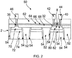
- FIG. 2 shows a semiconductor switch device 50 according to an embodiment of the present disclosure.
- the device 50 in this example is an NMOS switch device for use in RF applications.
- the device 50 includes a MOS field effect transistor comprising a source region 32, drain region 34, gate electrode 8, gate dielectric 6.
- the device also includes a body contact 36.
- the source region 32, drain region 34 and body contact 36 may be provided with electrical contacts 42, 44, 46, respectively (as is the gate electrode 8, although this is not shown in Figure 2 ).
- electrical contacts 42, 44, 46 may be connected to the source region 32, drain region 34 and body contact 36 by electrically conductive members 40 extending through one or more inter metal dielectric layers 62, 64, 66 (for example silicon oxide and silicon nitride) located provided on a major surface of the substrate 2.
- inter metal dielectric layers 62, 64, 66 for example silicon oxide and silicon nitride
- the source region 32 and drain region 34 in this example are located in a p-type well 80.
- the body contact 36 is located in another p-type well 70.
- Isolations regions 68 such as shallow trench isolation (STI) may be used to isolate the features located in the different wells.
- an optional buried p+ layer 82 may be located beneath the p-type well 80, and an optional buried p+ layer 72 may be located beneath the p-type well 70.
- Each well and buried p+ layer is connected through the underlying parts 74, 84 of the substrate 2, which may be p- doped.
- the wells 70, 80 and buried layers 72, 82 may also be separated by deep trench isolation 52 (DTI).
- the sidewalls of the DTI may be lined with one or more dielectric layers 54, such as silicon oxide.
- the p-type well 80, source region 32, drain region 34 and gate of the device 50 shown in Figure 2 may be formed using the method described herein (e.g. the method of Figure 1 ).
- Figure 4 compares the simulated off-state capacitance (C off ) of a conventional NMOS field effect transistor (plot labelled 204) with that of an NMOS field effect transistor made using a method of the kind described in relation to Figures 1A-1D (plot labelled 206). As can be seen from Figure 4 , an embodiment of this disclosure may produce an approximately 17% reduction in C off compared to a conventional NMOS field effect transistor.
- the baseline 208 corresponds to a conventional NMOS field effect transistor
- the plot 210 corresponds to an NMOS field effect transistor made using a method of the kind described in relation to Figures 1A-1D .
- the vertical axis in Figure 5 indicates the percentage change in C off in the plot 210, as a function of MTL, compared to the conventional device.
- a reduction in C off may be achieved across a range of values of MTL, and the largest gains are typically made at smaller mask tolerances.
- the method includes providing a semiconductor substrate having a major surface and a first semiconductor region having a first conductivity type located adjacent the major surface.
- the method also includes depositing a gate dielectric on the major surface.
- the method further includes implanting ions into the first semiconductor region through a mask positioned over the first semiconductor region, thereby to form a well region located in the first semiconductor region.
- the well region has a second conductivity type different to the first conductivity type.
- the method also includes depositing and patterning a gate electrode material on the gate dielectric to form a gate electrode located directly above the well region.
- the method further includes implanting ions into the first semiconductor region to form a source region and a drain region of the semiconductor switch device on either side of the gate electrode.
Landscapes
- Insulated Gate Type Field-Effect Transistor (AREA)
- Metal-Oxide And Bipolar Metal-Oxide Semiconductor Integrated Circuits (AREA)
Abstract
Description
- The present specification relates to method of making a semiconductor switch device and to a semiconductor switch device.
- Metal Oxide Semiconductor Field Effect Transistors (MOSFETs) can be used as electric switches for high Radio Frequency (RF) signals. For these applications the device does not actually switch at high frequencies, rather it passes or blocks RF signals. Best performance is achieved with a device that combines low series resistance in on-state with low input capacitance in off-state. One of the most popular ways to evaluate the overall performance of an RF Switch MOSFET is to calculate a figure of merit (FOM), which is defined as the product of the on-state resistance (Ron) and the off-state capacitance (Coff).
- Contributions to the off-state capacitance are the gate-to-source (Cgs), gate-to-drain (Cgd), gate-to-substrate (Cgb), drain-to-substrate (Cdb), and source-to-substrate (Csb) capacitance as shown in the following formulas:


- Here, Cds is the channel capacitance, and Csb, Cdb and Cgb are the source to bulk, drain to bulk and gate to bulk capacitances, respectively. The overlap capacitance (Cgs = Cgd) and parasitic junction capacitance (Cdb=Csb) are of great importance as they constitute both significant fractions of the total off-state capacitance (Coff). Therefore, to achieve low Coff, the overlap capacitance and parasitic junction capacitances need to be reduced.
- Aspects of the present disclosure are set out in the accompanying independent and dependent claims. Combinations of features from the dependent claims may be combined with features of the independent claims as appropriate and not merely as explicitly set out in the claims.
- According to an aspect of the present disclosure, there is provided a method of making a semiconductor switch device, the method comprising:
- providing a semiconductor substrate having:
- a major surface; and
- a first semiconductor region having a first conductivity type located adjacent the major surface;
- depositing a gate dielectric on the major surface of the substrate;
- implanting ions into the first semiconductor region through an opening in a mask positioned over the first semiconductor region, thereby to form a well region located in the first semiconductor region, the well region having a second conductivity type different to the first conductivity type;
- depositing and patterning a gate electrode material on the gate dielectric to form a gate electrode located directly above the well region; and
- implanting ions into the first semiconductor region to form a source region and a drain region of the semiconductor switch device on either side of the gate electrode.
- The use of the mask can prevent ions that are implanted to form the well region of the device from entering the parts of the first semiconductor region that will accommodate the source and drain regions on either side of the gate. This may allow the parasitic junction capacitances (Cdb=Csb) and, therefore, the off-state capacitance (Coff) of the device to be relatively low, owing to the reduced amount of impurity doping that occurs in the vicinity of the source and drain regions. Note that the gate electrode of the device is located directly above the well region, whereby a channel region of the device is located in the well region.
- The method may further include implanting ions into the first semiconductor region through the opening in the mask positioned over the first semiconductor region, thereby to adjust a threshold voltage of the semiconductor switch device. The mask can thus prevent at least some of these ions from entering the parts of the first semiconductor region that will accommodate the source and drain regions on either side of the gate. This may again allow the parasitic junction capacitance of the device to remain relatively low, even when ions are implanted for adjusting the threshold voltage (sometimes referred to as a DVt implant).
- The method may further include implanting ions into the first semiconductor region through the opening in the mask positioned over the first semiconductor region, thereby to inhibit punch-through in the semiconductor switch device. The mask can thus prevent at least some of these ions from entering the parts of the first semiconductor region that will accommodate the source and drain regions on either side of the gate. This may again allow the parasitic junction capacitance of the device to remain relatively low, even when ions are implanted to inhibit punch-through in the semiconductor switch device (sometimes referred to as an Anti-Punch-Through (APT) implant).
- A lateral dimension of the opening in the mask may be substantially equal to Lg+2*MTL, where Lg is a gate length of the semiconductor switch device, where MTL is a mask tolerance of the opening, and where MTL ≤ 600nm. In some embodiments, the mask tolerance MTL may be in the range 0 - 200nm. The gate length Lg may be in the sub-micron range.
- The ions implanted for forming the well region may comprise Boron ions.
- An implantation energy of the implant for forming the well region may be in the range 50keV - 4MeV.
- A peak concentration of the implanted ions of the implant for forming the well region may be at a depth of around 0.1 - 2 µm beneath the major surface of the semiconductor substrate.
- An implantation dose of the implant for forming the well region may be in the range 1011 - 1014 cm-2.
- The first conductivity type may be n-type and the second conductivity type may be p-type. However, it is envisaged that the first conductivity type may be p-type and the second conductivity type may be n-type.
- The method may include forming spacers on opposed sidewalls of the gate electrode prior to implanting the ions into the first semiconductor region to form the source region and the drain region. The spacers may be formed on the sidewalls of the gate electrode after the use of the aforementioned mask, whereby the formation of the spacers need not interfere with the use of the mask or any of the various implants that may be carried out through the mask.
- The first semiconductor region may be a doped epitaxial layer. The doped epitaxial layer may be provided as an upper layer on a Silicon-on-Insulator (SOI) substrate. In another example, the doped epitaxial layer may be provided on an underlying bulk semiconductor (e.g. silicon) substrate.
- According to another aspect of the present disclosure, there may be provided a semiconductor switch device made using the method described above. The semiconductor switch device may be a Radio Frequency (RF) switch device.
- A device of the kind described herein may be an RF switch device, for switching an RF signal. For the purposes of this disclosure "Radio Frequency" (RF) refers to frequencies typically in the range of, but not limited to 0.5 GHz ≤ f ≤ 90 GHz. Note that although a semiconductor switch device according to embodiments of this disclosure may be used to pass or block an RF signal, typically the device would not actually switch at the RF frequency itself.
- Embodiments of this disclosure will be described hereinafter, by way of example only, with reference to the accompanying drawings in which like reference signs relate to like elements and in which:
-
Figures 1A-1D show a method for making a field effect transistor of a semiconductor switch device according to an embodiment of the present disclosure; -
Figure 2 shows a semiconductor switch device according to an embodiment of the present disclosure; -
Figure 3 compares the simulated parasitic junction capacitance of a conventional field effect transistor with that of a field effect transistor made using a method of the kind shown inFigures 1A-1D ; -
Figure 4 compares the simulated off-state capacitance of a conventional field effect transistor with that of a field effect transistor made using a method of the kind shown inFigures 1A-1D ; and -
Figure 5 shows the impact of mask tolerance MTL (i.e. total mask opening = Lg +2MTL) on the off-state capacitance for a semiconductor switch device according to an embodiment of the present disclosure. - Embodiments of this disclosure are described in the following with reference to the accompanying drawings.
-
Figures 1A-1D the various stages in a show a method for making a field effect transistor of a semiconductor switch device according to an embodiment of the present disclosure. - In a first stage, shown in
Figure 1A , there is provided asemiconductor substrate 102. Thesubstrate 102 may, for instance, comprise silicon. Thesubstrate 102 has amajor surface 101. Thesubstrate 102 comprises afirst semiconductor region 108 having a first conductivity type located adjacent themajor surface 101. In this example, the first conductivity type is n-type, although is it envisaged that the first conductivity type may be p-type. - Where the first conductivity type is n-type, the
first semiconductor region 108 may be doped with Arsenic, Phosphorus or Antimony. On the other hand, where the first conductivity type is p-type, thefirst semiconductor region 108 may be doped with Boron or Indium. - In this example, the
first semiconductor region 108 comprises a doped epitaxial silicon layer located on an underlying part 106 (e.g. the bulk) of thesubstrate 102. The thickness of the epitaxial layer forming thefirst semiconductor region 108 may be around 0.1-1µm. Theunderlying part 106 may be have a second conductivity type, that is a different conductivity type to the first conductivity type of thefirst semiconductor region 108. Where the second conductivity type is p-type,underlying part 106 may be doped with Boron. On the other hand, where the second conductivity type is n-type, theunderlying part 106 may be doped with Arsenic. In the present example comprises p-type doped silicon. - As shown in
Figure 1 , adielectric layer 104 is deposited on themajor surface 101 of thesemiconductor substrate 102. Thedielectric layer 104 will subsequently be patterned to form a gate dielectric of the semiconductor switch device. Thedielectric layer 104 may, for instance, comprise silicon oxide. - In a next stage shown in
Figure 1 B , a number of ion implantation steps may be performed. Prior to implanting the ions, amask 110 may be positioned over themajor surface 101 of thesemiconductor substrate 102. Themask 110 has anopening 111. - As shown in
Figure 1 B , a lateral dimension of theopening 111 in themask 110 is substantially equal to Lg+2*MTL, wherein Lg is a gate length of the semiconductor switch device, and wherein MTL is a mask tolerance of the opening. It is envisaged that the mask tolerance MTL may be ≤ 600 nm. In a particular embodiment, the mask tolerance MTL may be in the range 0-200 nm. The gate length Lg of a semiconductor switch device of the kind described herein may be less than 1 µm. To summarise, the lateral dimension of theopening 111 in themask 110 is approximately equal to the gate length Lg, allowing also for the mask tolerance of theopening 111 through which the ions are to be implanted as described below. - Having positioned the
mask 110 over themajor surface 101 of thesemiconductor substrate 102, ions are implanted into the first semiconductor region through theopening 111. The implantation ions a represented by the arrows labelled A inFigure 1B . As shown inFigure 1B , the implanted ions form awell region 180 located in thefirst semiconductor region 108. Thewell region 180 will contain a channel region of the field effect transistor forming the semiconductor switch device. Thewell region 180 has the second conductivity type, which as noted above is different to the first conductivity type. Accordingly, in the present example, thewell region 180 is p-type, for forming an NMOS device. In examples in which the second conductivity type is n-type, thewell region 180 may accordingly be n-type, for forming a PMOS device. - Where the first conductivity type is n-type, the ions implanted for forming the
well region 180 may, for instance comprise Boron ions. An implantation energy of the ions implanted for forming thewell region 180 may be in the range 50keV - 4MeV, or more typically in the range of 100 - 300keV. A peak concentration of the implanted ions of the implant for forming thewell region 180 may be at a depth of around 0.1 - 2 µm beneath themajor surface 101 of thesemiconductor substrate 102. An implantation dose of the implant for forming thewell region 180 may be in the range 1011 - 1014 cm-2. - On the other hand, where the first conductivity type is p-type, the ions implanted for forming the
well region 180 may, for instance comprise Phosphorus (or Arsenic) ions. An implantation energy of the ions implanted for forming thewell region 180 may be in the range 100keV - 1MeV. A peak concentration of the implanted ions of the implant for forming thewell region 180 may be at a depth of around 0.1 - 2 µm µm beneath themajor surface 101 of thesemiconductor substrate 102. An implantation dose of the implant for forming thewell region 180 may be in the range 1011 - 1014 cm-2. - The
well region 180 formed by the implant may extend completely through thefirst semiconductor region 108. As shown inFigure 1B , thewell region 180 may extend partially into theunderling part 106 of thesubstrate 102. Thewell region 180 and theunderlying part 106 of thesemiconductor substrate 102 typically have the same conductivity type (i.e. the second conductivity type), which in the present example is p-type. - In addition to implanting ions for forming the
well region 180, one or more other implants may be performed. - For instance, in one example, ions may be implanted through the
opening 111 in themask 110 positioned over the first semiconductor region of thesemiconductor substrate 102, thereby to adjust a threshold voltage of the semiconductor switch device (this may be referred to as a DVt implant). - For an NMOS device (i.e. the first conductivity type is n-type, the second conductivity type is p-type), the ions implanted for adjusting a threshold voltage of the semiconductor switch device may, for instance, comprise Boron or Indium. An implantation energy of the ions implanted for adjusting the threshold voltage may be in the range 5 - 100keV. A peak concentration of the implanted ions of the implant for adjusting the threshold voltage may be at a depth of around 10 - 100 nm beneath the
major surface 101 of thesemiconductor substrate 102. An implantation dose of the implant for adjusting the threshold voltage may be in the range 1011 - 1014 cm-2. - On the other hand, for a PMOS device (i.e. the first conductivity type is p-type, the second conductivity type is n-type), the ions implanted for adjusting a threshold voltage of the semiconductor switch device may, for instance, comprise Arsenic, Phosphorus or Antimony. An implantation energy of the ions implanted for adjusting the threshold voltage may be in the range 5 - 200keV. A peak concentration of the implanted ions of the implant for adjusting the threshold voltage may be at a depth of around 10 - 100 nm beneath the
major surface 101 of thesemiconductor substrate 102. An implantation dose of the implant for adjusting the threshold voltage may be in the range 1011 - 1014 cm-2. - In another example, ions may be implanted through the
opening 111 in themask 110 positioned over the first semiconductor region of thesemiconductor substrate 102, thereby to inhibit punch-through in the semiconductor switch device (this may be referred to as an anti-punch-through, or "APT" implant). - For an NMOS device (i.e. the first conductivity type is n-type, the second conductivity type is p-type), the ions implanted for inhibiting punch-through in the semiconductor switch device may, for instance, comprise Boron. An implantation energy of the ions implanted for inhibiting punch-through may be in the range 10 - 200keV. A peak concentration of the implanted ions of the implant for inhibiting punch-through may be at a depth of around 0.1 - 2 µm beneath the
major surface 101 of thesemiconductor substrate 102. An implantation dose of the implant for inhibiting punch-through may be in the range 1011 - 1014 cm-2. - On the other hand, for a PMOS device (i.e. the first conductivity type is p-type, the second conductivity type is n-type), the ions implanted for inhibiting punch-through in the semiconductor switch device may, for instance, comprise Phosphorus. An implantation energy of the ions implanted for inhibiting punch-through may be in the range 50 - 200 keV. A peak concentration of the implanted ions of the implant for inhibiting punch-through may be at a depth of around 0.1 - 2 µm beneath the
major surface 101 of thesemiconductor substrate 102. An implantation dose of the implant for inhibiting punch-through may be in the range 1011 - 1014 cm-2. - In a next stage shown in
Figure 1C , following removal of themask 110, a gate of the field effect transistor may be formed. This may be achieved by depositing a gate electrode material (e.g. doped polysilicon) over thedielectric layer 104, and then patterning the gate electrode material and thedielectric layer 104 to reach the arrangement shown inFigure 1C . The gate may include agate electrode 118 located on a remainingpart 105 of theaforementioned dielectric layer 104. As discussed above, the gate has a gate length Lg. The gate is located directly above thewell region 180. Note that since theopening 111 in themask 110 described above had a lateral dimension given by Lg+2*MTL, the gate may be approximately the same size (laterally) as thewell region 180, at least at positions close to themajor surface 101 of thesemiconductor substrate 102. - In a next stage shown in Figure ID, the gate may be provided with
sidewall spacers 126. As is known in the art, alayer 124 comprising Silicon Oxide may be deposited over the gate electrode prior to the formation of thespacers 126. Thelayer 124 may cover at least the sidewalls of the gate electrode. Thespacers 126 may partially mask the parts of thefirst semiconductor region 108 located immediately on either side of the gate, during formation of the source and drain regions to be described below. - Following the optional formation of the
spacers 126, asource region 120 and drainregion 140 of the device may be formed on either side of the gate electrode using ion implantation. As can be seen inFigure 1D , the source and drainregions first semiconductor region 108 close to themajor surface 101 of thesemiconductor substrate 102, and may extend inwards towards the peripheral edges of thewell region 180. The source and drain region are both of the first conductivity type (n-type in the present example). For an NMOS device (i.e. the first conductivity type is n-type, the second conductivity type is p-type), the ions implanted for forming the source and drain regions may, for instance, comprise Arsenic, Phosphorus (or Antimony). On the other hand, for a PMOS device (i.e. the first conductivity type is p-type, the second conductivity type is n-type), the ions implanted for forming the source and drain regions may, for instance, comprise Boron (or Indium). - It is also envisaged that
LDD regions spacers 126 using ion implantation. TheseLDD regions regions regions LDD regions regions Figure 1D , theLDD regions regions well region 180. - With reference to
Figures 1B and1D , it will be appreciated that the use of themask 110 during the implantation steps for forming thewell region 180, for adjusting the threshold voltage and for inhibiting punch-through can prevent the ions associated with these implants entering the parts of thefirst semiconductor region 108 which will subsequently be occupied by thesource region 120 and thedrain region 140. This may allow the parasitic junction capacitances (Cdb, Cds) and, therefore, the off-state capacitance (Coff) of the device to be relatively low, owing to the reduced amount of impurity doping that occurs in the vicinity of thesource region 120 anddrain regions 140. -
Figure 2 shows asemiconductor switch device 50 according to an embodiment of the present disclosure. Thedevice 50 in this example is an NMOS switch device for use in RF applications. Thedevice 50 includes a MOS field effect transistor comprising asource region 32,drain region 34,gate electrode 8,gate dielectric 6. The device also includes abody contact 36. Thesource region 32,drain region 34 andbody contact 36 may be provided withelectrical contacts gate electrode 8, although this is not shown inFigure 2 ). Theseelectrical contacts source region 32,drain region 34 andbody contact 36 by electricallyconductive members 40 extending through one or more inter metal dielectric layers 62, 64, 66 (for example silicon oxide and silicon nitride) located provided on a major surface of thesubstrate 2. - The
source region 32 and drainregion 34 in this example are located in a p-type well 80. Thebody contact 36 is located in another p-type well 70. Isolations regions 68 (such as shallow trench isolation (STI)) may be used to isolate the features located in the different wells. In this example, an optional buriedp+ layer 82 may be located beneath the p-type well 80, and an optional buriedp+ layer 72 may be located beneath the p-type well 70. Each well and buried p+ layer is connected through theunderlying parts substrate 2, which may be p- doped. Thewells layers dielectric layers 54, such as silicon oxide. - The p-
type well 80,source region 32,drain region 34 and gate of thedevice 50 shown inFigure 2 may be formed using the method described herein (e.g. the method ofFigure 1 ). -
Figure 3 compares the simulated parasitic junction capacitance (Cdb=Csb), as a function of frequency, of a conventional NMOS field effect transistor (plot labelled 200) with that of an NMOS field effect transistor made using a method of the kind described in relation toFigures 1A-1D (plot labelled 202). As can be seen fromFigure 3 , an embodiment of this disclosure may produce an approximately 50% reduction in parasitic junction capacitance compared to a conventional NMOS field effect transistor. -
Figure 4 compares the simulated off-state capacitance (Coff) of a conventional NMOS field effect transistor (plot labelled 204) with that of an NMOS field effect transistor made using a method of the kind described in relation toFigures 1A-1D (plot labelled 206). As can be seen fromFigure 4 , an embodiment of this disclosure may produce an approximately 17% reduction in Coff compared to a conventional NMOS field effect transistor. -
Figure 5 shows the impact of mask tolerance MTL (i.e. total mask opening = Lg +2MTL) on the off-state capacitance (Coff) for a semiconductor switch device (NMOS) according to an embodiment of the present disclosure. InFigure 5 , thebaseline 208 corresponds to a conventional NMOS field effect transistor, while theplot 210 corresponds to an NMOS field effect transistor made using a method of the kind described in relation toFigures 1A-1D . The vertical axis inFigure 5 indicates the percentage change in Coff in theplot 210, as a function of MTL, compared to the conventional device. As can be seen inFigure 5 , a reduction in Coff may be achieved across a range of values of MTL, and the largest gains are typically made at smaller mask tolerances. - Accordingly, there has been described a method of making a semiconductor switch device. The method includes providing a semiconductor substrate having a major surface and a first semiconductor region having a first conductivity type located adjacent the major surface. The method also includes depositing a gate dielectric on the major surface. The method further includes implanting ions into the first semiconductor region through a mask positioned over the first semiconductor region, thereby to form a well region located in the first semiconductor region. The well region has a second conductivity type different to the first conductivity type. The method also includes depositing and patterning a gate electrode material on the gate dielectric to form a gate electrode located directly above the well region. The method further includes implanting ions into the first semiconductor region to form a source region and a drain region of the semiconductor switch device on either side of the gate electrode.
- Although particular embodiments of this disclosure have been described, it will be appreciated that many modifications/additions and/or substitutions may be made within the scope of the claims.
Claims (15)
- A method of making a semiconductor switch device, the method comprising:providing a semiconductor substrate having:a major surface; anda first semiconductor region having a first conductivity type located adjacent the major surface;depositing a gate dielectric on the major surface of the substrate;implanting ions into the first semiconductor region through an opening in a mask positioned over the first semiconductor region, thereby to form a well region located in the first semiconductor region, the well region having a second conductivity type different to the first conductivity type;depositing and patterning a gate electrode material on the gate dielectric to form a gate electrode located directly above the well region; andimplanting ions into the first semiconductor region to form a source region and a drain region of the semiconductor switch device on either side of the gate electrode.
- The method of claim 1, further comprising implanting ions into the first semiconductor region through the opening in the mask positioned over the first semiconductor region, thereby to adjust a threshold voltage of the semiconductor switch device.
- The method of claim 1 or claim 2, further comprising implanting ions into the first semiconductor region through the opening in the mask positioned over the first semiconductor region, thereby to inhibit punch-through in the semiconductor switch device.
- The method of any preceding claim, wherein a lateral dimension of the opening in the mask is substantially equal to Lg+2*MTL, wherein Lg is a gate length of the semiconductor switch device, wherein MTL is a mask tolerance of the opening, and wherein MTL ≤ 600 nm.
- The method of claim 4, wherein the mask tolerance MTL is in the range 0 - 200 nm.
- The method of claim 4 or claim 5, wherein the gate length Lg is less than 1 µm.
- The method of any preceding claim, wherein the ions implanted for forming the well region comprise Boron ions.
- The method of any preceding claim, wherein an implantation energy of the implant for forming the well region is in the range 50keV- 4MeV.
- The method of any preceding claim, wherein a peak concentration of the implanted ions of the implant for forming the well region is at a depth of around 0.1 - 2 µm beneath the major surface of the semiconductor substrate.
- The method of any preceding claim, wherein an implantation dose of the implant for forming the well region is in the range 1011 - 1014 cm-2.
- The method of any preceding claim, wherein the first conductivity type is n-type and wherein the second conductivity type is p-type.
- The method of any preceding claim, comprising forming spacers on opposed sidewalls of the gate electrode prior to implanting the ions into the first semiconductor region to form the source region and the drain region.
- The method of any preceding claim, wherein the first semiconductor region comprises a doped epitaxial layer.
- A semiconductor switch device made using the method of any preceding claim.
- The device of claim 14, wherein the device is a Radio Frequency (RF) switch device.
Priority Applications (3)
| Application Number | Priority Date | Filing Date | Title |
|---|---|---|---|
| EP17154466.1A EP3358626B1 (en) | 2017-02-02 | 2017-02-02 | Method of making a semiconductor switch device |
| US15/886,265 US10490407B2 (en) | 2017-02-02 | 2018-02-01 | Method of making a semiconductor switch device |
| CN201810109135.XA CN108417634B (en) | 2017-02-02 | 2018-02-02 | Method of manufacturing semiconductor switching device |
Applications Claiming Priority (1)
| Application Number | Priority Date | Filing Date | Title |
|---|---|---|---|
| EP17154466.1A EP3358626B1 (en) | 2017-02-02 | 2017-02-02 | Method of making a semiconductor switch device |
Publications (2)
| Publication Number | Publication Date |
|---|---|
| EP3358626A1 true EP3358626A1 (en) | 2018-08-08 |
| EP3358626B1 EP3358626B1 (en) | 2022-07-20 |
Family
ID=57963081
Family Applications (1)
| Application Number | Title | Priority Date | Filing Date |
|---|---|---|---|
| EP17154466.1A Active EP3358626B1 (en) | 2017-02-02 | 2017-02-02 | Method of making a semiconductor switch device |
Country Status (3)
| Country | Link |
|---|---|
| US (1) | US10490407B2 (en) |
| EP (1) | EP3358626B1 (en) |
| CN (1) | CN108417634B (en) |
Families Citing this family (2)
| Publication number | Priority date | Publication date | Assignee | Title |
|---|---|---|---|---|
| US10930747B2 (en) | 2019-06-04 | 2021-02-23 | Nxp B.V. | Semiconductor device with an encircled electrode |
| US11018230B1 (en) | 2019-12-20 | 2021-05-25 | Nxp B.V. | Semiconductor devices with a mixed crystal region |
Citations (4)
| Publication number | Priority date | Publication date | Assignee | Title |
|---|---|---|---|---|
| US4108686A (en) * | 1977-07-22 | 1978-08-22 | Rca Corp. | Method of making an insulated gate field effect transistor by implanted double counterdoping |
| US6342413B1 (en) * | 1999-10-22 | 2002-01-29 | Nec Corporation | Method of manufacturing semiconductor device |
| US20020096697A1 (en) * | 1999-05-21 | 2002-07-25 | Jenoe Tihanyi | Junction-isolated lateral mosfet for high-/low-side switches |
| US20100164017A1 (en) * | 2004-09-27 | 2010-07-01 | Panasonic Corporation | Semiconductor device and method for fabricating the same |
Family Cites Families (39)
| Publication number | Priority date | Publication date | Assignee | Title |
|---|---|---|---|---|
| US4306916A (en) | 1979-09-20 | 1981-12-22 | American Microsystems, Inc. | CMOS P-Well selective implant method |
| US5648281A (en) * | 1992-09-21 | 1997-07-15 | Siliconix Incorporated | Method for forming an isolation structure and a bipolar transistor on a semiconductor substrate |
| US5614430A (en) * | 1996-03-11 | 1997-03-25 | Taiwan Semiconductor Manufacturing Company Ltd. | Anti-punchthrough ion implantation for sub-half micron channel length MOSFET devices |
| KR19980039470A (en) * | 1996-11-27 | 1998-08-17 | 김광호 | Manufacturing method of semiconductor device |
| JPH1174506A (en) * | 1997-07-02 | 1999-03-16 | Mitsubishi Electric Corp | Semiconductor device and manufacturing method thereof |
| JP3070732B2 (en) * | 1997-11-13 | 2000-07-31 | 日本電気株式会社 | Method for manufacturing MOS semiconductor device |
| US6297082B1 (en) * | 1999-08-25 | 2001-10-02 | United Microelectronics Corp. | Method of fabricating a MOS transistor with local channel ion implantation regions |
| US6391752B1 (en) * | 2000-09-12 | 2002-05-21 | Taiwan Semiconductor Manufacturing, Co., Ltd. | Method of fabricating a silicon-on-insulator semiconductor device with an implanted ground plane |
| US20020109206A1 (en) * | 2000-12-14 | 2002-08-15 | Klaus Schimpf | Lateral PNP-type transistor based on a vertical NPN-structure and process for producing such PNP-type transistor |
| US6603181B2 (en) * | 2001-01-16 | 2003-08-05 | International Business Machines Corporation | MOS device having a passivated semiconductor-dielectric interface |
| KR20030016900A (en) * | 2001-08-23 | 2003-03-03 | 삼성전자주식회사 | Method of forming pmos transistor in dual gate cmos type semiconductor device |
| US20040188774A1 (en) * | 2003-03-31 | 2004-09-30 | Sanyo Electric Co., Ltd. | Semiconductor device and method of fabricating semiconductor device |
| US7473929B2 (en) * | 2003-07-02 | 2009-01-06 | Panasonic Corporation | Semiconductor device and method for fabricating the same |
| US7126382B2 (en) * | 2003-08-29 | 2006-10-24 | Intel Corporation | Lower power high speed design in BiCMOS processes |
| US7413957B2 (en) * | 2004-06-24 | 2008-08-19 | Applied Materials, Inc. | Methods for forming a transistor |
| US20060022526A1 (en) * | 2004-07-27 | 2006-02-02 | David Cartalade | Asymmetric radio-frequency switch |
| US7528040B2 (en) * | 2005-05-24 | 2009-05-05 | Cree, Inc. | Methods of fabricating silicon carbide devices having smooth channels |
| WO2006131986A1 (en) * | 2005-06-10 | 2006-12-14 | Fujitsu Limited | Semiconductor device, semiconductor system and semiconductor device manufacturing method |
| JP4967478B2 (en) * | 2006-06-30 | 2012-07-04 | 富士通セミコンダクター株式会社 | Semiconductor device and manufacturing method thereof |
| US7790543B2 (en) * | 2008-01-11 | 2010-09-07 | International Business Machines Corporation | Device structures for a metal-oxide-semiconductor field effect transistor and methods of fabricating such device structures |
| DE102008006961A1 (en) * | 2008-01-31 | 2009-08-27 | Advanced Micro Devices, Inc., Sunnyvale | A method of creating a deformed channel region in a transistor by deep implantation of a strain inducing species under the channel region |
| US8030151B2 (en) * | 2009-03-27 | 2011-10-04 | National Semiconductor Corporation | Configuration and fabrication of semiconductor structure having bipolar junction transistor in which non-monocrystalline semiconductor spacing portion controls base-link length |
| KR20100111906A (en) * | 2009-04-08 | 2010-10-18 | 삼성전자주식회사 | Semiconductor device |
| US8003455B2 (en) | 2009-05-21 | 2011-08-23 | International Business Machines Corporation | Implantation using a hardmask |
| US8193560B2 (en) * | 2009-06-18 | 2012-06-05 | Freescale Semiconductor, Inc. | Voltage limiting devices |
| WO2011050464A1 (en) * | 2009-10-30 | 2011-05-05 | Sidense Corp. | Twin well split-channel otp memory cell |
| CN102403230B (en) * | 2010-09-17 | 2014-05-14 | 中芯国际集成电路制造(上海)有限公司 | Manufacturing method of semiconductor device structure |
| US20120244668A1 (en) * | 2011-03-25 | 2012-09-27 | Jeesung Jung | Semiconductor devices with layout controlled channel and associated processes of manufacturing |
| US20120267724A1 (en) * | 2011-04-20 | 2012-10-25 | Globalfoundries Inc. | Mos semiconductor device and methods for its fabrication |
| CN102779753B (en) * | 2011-05-12 | 2015-05-06 | 中芯国际集成电路制造(上海)有限公司 | Manufacture method of semiconductor device |
| US8581625B2 (en) * | 2011-05-19 | 2013-11-12 | Semiconductor Energy Laboratory Co., Ltd. | Programmable logic device |
| CN103165457A (en) * | 2011-12-15 | 2013-06-19 | 中国科学院微电子研究所 | Semiconductor device manufacturing method |
| US9257463B2 (en) * | 2012-05-31 | 2016-02-09 | Taiwan Semiconductor Manufacturing Company, Ltd. | Self-aligned implantation process for forming junction isolation regions |
| US8883584B2 (en) * | 2012-07-03 | 2014-11-11 | Institute of Microelectronics, Chinese Academy of Sciences | Method of manufacturing semiconductor device with well etched spacer |
| US9177986B2 (en) * | 2012-08-29 | 2015-11-03 | Taiwan Semiconductor Manufacturing Company, Ltd. | Isolation for semiconductor devices |
| CN104051529B (en) * | 2013-03-13 | 2017-07-28 | 台湾积体电路制造股份有限公司 | RF switches on high-impedance substrate |
| US9583342B2 (en) * | 2014-07-24 | 2017-02-28 | Taiwan Semiconductor Manufacturing Company, Ltd. | FinFET doping methods and structures thereof |
| CN105448916B (en) * | 2014-08-29 | 2018-10-16 | 中芯国际集成电路制造(上海)有限公司 | Transistor and forming method thereof |
| EP3200235A1 (en) | 2016-01-28 | 2017-08-02 | Nxp B.V. | Semiconductor switch device and a method of making a semiconductor switch device |
-
2017
- 2017-02-02 EP EP17154466.1A patent/EP3358626B1/en active Active
-
2018
- 2018-02-01 US US15/886,265 patent/US10490407B2/en active Active
- 2018-02-02 CN CN201810109135.XA patent/CN108417634B/en active Active
Patent Citations (4)
| Publication number | Priority date | Publication date | Assignee | Title |
|---|---|---|---|---|
| US4108686A (en) * | 1977-07-22 | 1978-08-22 | Rca Corp. | Method of making an insulated gate field effect transistor by implanted double counterdoping |
| US20020096697A1 (en) * | 1999-05-21 | 2002-07-25 | Jenoe Tihanyi | Junction-isolated lateral mosfet for high-/low-side switches |
| US6342413B1 (en) * | 1999-10-22 | 2002-01-29 | Nec Corporation | Method of manufacturing semiconductor device |
| US20100164017A1 (en) * | 2004-09-27 | 2010-07-01 | Panasonic Corporation | Semiconductor device and method for fabricating the same |
Also Published As
| Publication number | Publication date |
|---|---|
| CN108417634A (en) | 2018-08-17 |
| CN108417634B (en) | 2023-09-15 |
| US20180218906A1 (en) | 2018-08-02 |
| EP3358626B1 (en) | 2022-07-20 |
| US10490407B2 (en) | 2019-11-26 |
Similar Documents
| Publication | Publication Date | Title |
|---|---|---|
| US9660074B2 (en) | Methods and apparatus for LDMOS devices with cascaded RESURF implants and double buffers | |
| US9059275B2 (en) | Semiconductor device | |
| US8178930B2 (en) | Structure to improve MOS transistor on-breakdown voltage | |
| US8674442B2 (en) | Semiconductor device and manufacturing method thereof | |
| US7928508B2 (en) | Disconnected DPW structures for improving on-state performance of MOS devices | |
| US9741793B2 (en) | Semiconductor device with false drain | |
| US11329156B2 (en) | Transistor with extended drain region | |
| US7151296B2 (en) | High voltage lateral diffused MOSFET device | |
| US11374124B2 (en) | Protection of drain extended transistor field oxide | |
| US20050253191A1 (en) | Robust DEMOS transistors and method for making the same | |
| US11152505B2 (en) | Drain extended transistor | |
| WO2015134909A1 (en) | Ldmos transistor and method of forming the ldmos transistor with improved rds*cgd | |
| US11742422B2 (en) | Semiconductor device and method of fabricating the same | |
| US10566423B2 (en) | Semiconductor switch device and a method of making a semiconductor switch device | |
| US10490407B2 (en) | Method of making a semiconductor switch device | |
| US10749023B2 (en) | Vertical transistor with extended drain region | |
| US9013004B2 (en) | Quasi-vertical structure having a sidewall implantation for high voltage MOS device | |
| US10431666B2 (en) | Method of making a semiconductor switch device | |
| US10158002B2 (en) | Semiconductor switch device | |
| EP3599645A1 (en) | Semiconductor device with drain active area | |
| WO2002003468A2 (en) | A novel capacitively coupled dtmos on soi | |
| US10608108B2 (en) | Extended drain MOSFETs (EDMOS) |
Legal Events
| Date | Code | Title | Description |
|---|---|---|---|
| PUAI | Public reference made under article 153(3) epc to a published international application that has entered the european phase |
Free format text: ORIGINAL CODE: 0009012 |
|
| STAA | Information on the status of an ep patent application or granted ep patent |
Free format text: STATUS: THE APPLICATION HAS BEEN PUBLISHED |
|
| AK | Designated contracting states |
Kind code of ref document: A1 Designated state(s): AL AT BE BG CH CY CZ DE DK EE ES FI FR GB GR HR HU IE IS IT LI LT LU LV MC MK MT NL NO PL PT RO RS SE SI SK SM TR |
|
| AX | Request for extension of the european patent |
Extension state: BA ME |
|
| STAA | Information on the status of an ep patent application or granted ep patent |
Free format text: STATUS: REQUEST FOR EXAMINATION WAS MADE |
|
| 17P | Request for examination filed |
Effective date: 20190208 |
|
| RBV | Designated contracting states (corrected) |
Designated state(s): AL AT BE BG CH CY CZ DE DK EE ES FI FR GB GR HR HU IE IS IT LI LT LU LV MC MK MT NL NO PL PT RO RS SE SI SK SM TR |
|
| STAA | Information on the status of an ep patent application or granted ep patent |
Free format text: STATUS: EXAMINATION IS IN PROGRESS |
|
| 17Q | First examination report despatched |
Effective date: 20200420 |
|
| REG | Reference to a national code |
Ref country code: DE Ref legal event code: R079 Ref document number: 602017059574 Country of ref document: DE Free format text: PREVIOUS MAIN CLASS: H01L0029660000 Ipc: H01L0021336000 |
|
| RIC1 | Information provided on ipc code assigned before grant |
Ipc: H01L 29/10 20060101ALI20220310BHEP Ipc: H01L 29/78 20060101ALI20220310BHEP Ipc: H01L 21/8234 20060101ALI20220310BHEP Ipc: H01L 21/336 20060101AFI20220310BHEP |
|
| GRAP | Despatch of communication of intention to grant a patent |
Free format text: ORIGINAL CODE: EPIDOSNIGR1 |
|
| STAA | Information on the status of an ep patent application or granted ep patent |
Free format text: STATUS: GRANT OF PATENT IS INTENDED |
|
| INTG | Intention to grant announced |
Effective date: 20220419 |
|
| GRAS | Grant fee paid |
Free format text: ORIGINAL CODE: EPIDOSNIGR3 |
|
| GRAA | (expected) grant |
Free format text: ORIGINAL CODE: 0009210 |
|
| STAA | Information on the status of an ep patent application or granted ep patent |
Free format text: STATUS: THE PATENT HAS BEEN GRANTED |
|
| AK | Designated contracting states |
Kind code of ref document: B1 Designated state(s): AL AT BE BG CH CY CZ DE DK EE ES FI FR GB GR HR HU IE IS IT LI LT LU LV MC MK MT NL NO PL PT RO RS SE SI SK SM TR |
|
| REG | Reference to a national code |
Ref country code: CH Ref legal event code: EP |
|
| REG | Reference to a national code |
Ref country code: DE Ref legal event code: R096 Ref document number: 602017059574 Country of ref document: DE |
|
| REG | Reference to a national code |
Ref country code: AT Ref legal event code: REF Ref document number: 1506081 Country of ref document: AT Kind code of ref document: T Effective date: 20220815 |
|
| REG | Reference to a national code |
Ref country code: IE Ref legal event code: FG4D |
|
| REG | Reference to a national code |
Ref country code: LT Ref legal event code: MG9D |
|
| REG | Reference to a national code |
Ref country code: NL Ref legal event code: MP Effective date: 20220720 |
|
| PG25 | Lapsed in a contracting state [announced via postgrant information from national office to epo] |
Ref country code: SE Free format text: LAPSE BECAUSE OF FAILURE TO SUBMIT A TRANSLATION OF THE DESCRIPTION OR TO PAY THE FEE WITHIN THE PRESCRIBED TIME-LIMIT Effective date: 20220720 Ref country code: RS Free format text: LAPSE BECAUSE OF FAILURE TO SUBMIT A TRANSLATION OF THE DESCRIPTION OR TO PAY THE FEE WITHIN THE PRESCRIBED TIME-LIMIT Effective date: 20220720 Ref country code: PT Free format text: LAPSE BECAUSE OF FAILURE TO SUBMIT A TRANSLATION OF THE DESCRIPTION OR TO PAY THE FEE WITHIN THE PRESCRIBED TIME-LIMIT Effective date: 20221121 Ref country code: NO Free format text: LAPSE BECAUSE OF FAILURE TO SUBMIT A TRANSLATION OF THE DESCRIPTION OR TO PAY THE FEE WITHIN THE PRESCRIBED TIME-LIMIT Effective date: 20221020 Ref country code: NL Free format text: LAPSE BECAUSE OF FAILURE TO SUBMIT A TRANSLATION OF THE DESCRIPTION OR TO PAY THE FEE WITHIN THE PRESCRIBED TIME-LIMIT Effective date: 20220720 Ref country code: LV Free format text: LAPSE BECAUSE OF FAILURE TO SUBMIT A TRANSLATION OF THE DESCRIPTION OR TO PAY THE FEE WITHIN THE PRESCRIBED TIME-LIMIT Effective date: 20220720 Ref country code: LT Free format text: LAPSE BECAUSE OF FAILURE TO SUBMIT A TRANSLATION OF THE DESCRIPTION OR TO PAY THE FEE WITHIN THE PRESCRIBED TIME-LIMIT Effective date: 20220720 Ref country code: FI Free format text: LAPSE BECAUSE OF FAILURE TO SUBMIT A TRANSLATION OF THE DESCRIPTION OR TO PAY THE FEE WITHIN THE PRESCRIBED TIME-LIMIT Effective date: 20220720 Ref country code: ES Free format text: LAPSE BECAUSE OF FAILURE TO SUBMIT A TRANSLATION OF THE DESCRIPTION OR TO PAY THE FEE WITHIN THE PRESCRIBED TIME-LIMIT Effective date: 20220720 |
|
| REG | Reference to a national code |
Ref country code: AT Ref legal event code: MK05 Ref document number: 1506081 Country of ref document: AT Kind code of ref document: T Effective date: 20220720 |
|
| PG25 | Lapsed in a contracting state [announced via postgrant information from national office to epo] |
Ref country code: PL Free format text: LAPSE BECAUSE OF FAILURE TO SUBMIT A TRANSLATION OF THE DESCRIPTION OR TO PAY THE FEE WITHIN THE PRESCRIBED TIME-LIMIT Effective date: 20220720 Ref country code: IS Free format text: LAPSE BECAUSE OF FAILURE TO SUBMIT A TRANSLATION OF THE DESCRIPTION OR TO PAY THE FEE WITHIN THE PRESCRIBED TIME-LIMIT Effective date: 20221120 Ref country code: HR Free format text: LAPSE BECAUSE OF FAILURE TO SUBMIT A TRANSLATION OF THE DESCRIPTION OR TO PAY THE FEE WITHIN THE PRESCRIBED TIME-LIMIT Effective date: 20220720 Ref country code: GR Free format text: LAPSE BECAUSE OF FAILURE TO SUBMIT A TRANSLATION OF THE DESCRIPTION OR TO PAY THE FEE WITHIN THE PRESCRIBED TIME-LIMIT Effective date: 20221021 |
|
| REG | Reference to a national code |
Ref country code: DE Ref legal event code: R097 Ref document number: 602017059574 Country of ref document: DE |
|
| PG25 | Lapsed in a contracting state [announced via postgrant information from national office to epo] |
Ref country code: SM Free format text: LAPSE BECAUSE OF FAILURE TO SUBMIT A TRANSLATION OF THE DESCRIPTION OR TO PAY THE FEE WITHIN THE PRESCRIBED TIME-LIMIT Effective date: 20220720 Ref country code: RO Free format text: LAPSE BECAUSE OF FAILURE TO SUBMIT A TRANSLATION OF THE DESCRIPTION OR TO PAY THE FEE WITHIN THE PRESCRIBED TIME-LIMIT Effective date: 20220720 Ref country code: DK Free format text: LAPSE BECAUSE OF FAILURE TO SUBMIT A TRANSLATION OF THE DESCRIPTION OR TO PAY THE FEE WITHIN THE PRESCRIBED TIME-LIMIT Effective date: 20220720 Ref country code: CZ Free format text: LAPSE BECAUSE OF FAILURE TO SUBMIT A TRANSLATION OF THE DESCRIPTION OR TO PAY THE FEE WITHIN THE PRESCRIBED TIME-LIMIT Effective date: 20220720 Ref country code: AT Free format text: LAPSE BECAUSE OF FAILURE TO SUBMIT A TRANSLATION OF THE DESCRIPTION OR TO PAY THE FEE WITHIN THE PRESCRIBED TIME-LIMIT Effective date: 20220720 |
|
| PLBE | No opposition filed within time limit |
Free format text: ORIGINAL CODE: 0009261 |
|
| STAA | Information on the status of an ep patent application or granted ep patent |
Free format text: STATUS: NO OPPOSITION FILED WITHIN TIME LIMIT |
|
| PG25 | Lapsed in a contracting state [announced via postgrant information from national office to epo] |
Ref country code: SK Free format text: LAPSE BECAUSE OF FAILURE TO SUBMIT A TRANSLATION OF THE DESCRIPTION OR TO PAY THE FEE WITHIN THE PRESCRIBED TIME-LIMIT Effective date: 20220720 Ref country code: EE Free format text: LAPSE BECAUSE OF FAILURE TO SUBMIT A TRANSLATION OF THE DESCRIPTION OR TO PAY THE FEE WITHIN THE PRESCRIBED TIME-LIMIT Effective date: 20220720 |
|
| 26N | No opposition filed |
Effective date: 20230421 |
|
| PG25 | Lapsed in a contracting state [announced via postgrant information from national office to epo] |
Ref country code: AL Free format text: LAPSE BECAUSE OF FAILURE TO SUBMIT A TRANSLATION OF THE DESCRIPTION OR TO PAY THE FEE WITHIN THE PRESCRIBED TIME-LIMIT Effective date: 20220720 |
|
| P01 | Opt-out of the competence of the unified patent court (upc) registered |
Effective date: 20230725 |
|
| PG25 | Lapsed in a contracting state [announced via postgrant information from national office to epo] |
Ref country code: SI Free format text: LAPSE BECAUSE OF FAILURE TO SUBMIT A TRANSLATION OF THE DESCRIPTION OR TO PAY THE FEE WITHIN THE PRESCRIBED TIME-LIMIT Effective date: 20220720 |
|
| PG25 | Lapsed in a contracting state [announced via postgrant information from national office to epo] |
Ref country code: MC Free format text: LAPSE BECAUSE OF FAILURE TO SUBMIT A TRANSLATION OF THE DESCRIPTION OR TO PAY THE FEE WITHIN THE PRESCRIBED TIME-LIMIT Effective date: 20220720 |
|
| REG | Reference to a national code |
Ref country code: CH Ref legal event code: PL |
|
| REG | Reference to a national code |
Ref country code: BE Ref legal event code: MM Effective date: 20230228 |
|
| GBPC | Gb: european patent ceased through non-payment of renewal fee |
Effective date: 20230202 |
|
| PG25 | Lapsed in a contracting state [announced via postgrant information from national office to epo] |
Ref country code: LU Free format text: LAPSE BECAUSE OF NON-PAYMENT OF DUE FEES Effective date: 20230202 Ref country code: LI Free format text: LAPSE BECAUSE OF NON-PAYMENT OF DUE FEES Effective date: 20230228 Ref country code: CH Free format text: LAPSE BECAUSE OF NON-PAYMENT OF DUE FEES Effective date: 20230228 |
|
| REG | Reference to a national code |
Ref country code: IE Ref legal event code: MM4A |
|
| PG25 | Lapsed in a contracting state [announced via postgrant information from national office to epo] |
Ref country code: GB Free format text: LAPSE BECAUSE OF NON-PAYMENT OF DUE FEES Effective date: 20230202 |
|
| PG25 | Lapsed in a contracting state [announced via postgrant information from national office to epo] |
Ref country code: IE Free format text: LAPSE BECAUSE OF NON-PAYMENT OF DUE FEES Effective date: 20230202 Ref country code: GB Free format text: LAPSE BECAUSE OF NON-PAYMENT OF DUE FEES Effective date: 20230202 |
|
| PG25 | Lapsed in a contracting state [announced via postgrant information from national office to epo] |
Ref country code: BE Free format text: LAPSE BECAUSE OF NON-PAYMENT OF DUE FEES Effective date: 20230228 |
|
| PG25 | Lapsed in a contracting state [announced via postgrant information from national office to epo] |
Ref country code: IT Free format text: LAPSE BECAUSE OF FAILURE TO SUBMIT A TRANSLATION OF THE DESCRIPTION OR TO PAY THE FEE WITHIN THE PRESCRIBED TIME-LIMIT Effective date: 20220720 |
|
| PG25 | Lapsed in a contracting state [announced via postgrant information from national office to epo] |
Ref country code: BG Free format text: LAPSE BECAUSE OF FAILURE TO SUBMIT A TRANSLATION OF THE DESCRIPTION OR TO PAY THE FEE WITHIN THE PRESCRIBED TIME-LIMIT Effective date: 20220720 |
|
| REG | Reference to a national code |
Ref country code: DE Ref legal event code: R079 Ref document number: 602017059574 Country of ref document: DE Free format text: PREVIOUS MAIN CLASS: H01L0021336000 Ipc: H10D0030010000 |
|
| PG25 | Lapsed in a contracting state [announced via postgrant information from national office to epo] |
Ref country code: BG Free format text: LAPSE BECAUSE OF FAILURE TO SUBMIT A TRANSLATION OF THE DESCRIPTION OR TO PAY THE FEE WITHIN THE PRESCRIBED TIME-LIMIT Effective date: 20220720 |
|
| PG25 | Lapsed in a contracting state [announced via postgrant information from national office to epo] |
Ref country code: CY Free format text: LAPSE BECAUSE OF FAILURE TO SUBMIT A TRANSLATION OF THE DESCRIPTION OR TO PAY THE FEE WITHIN THE PRESCRIBED TIME-LIMIT; INVALID AB INITIO Effective date: 20170202 |
|
| PG25 | Lapsed in a contracting state [announced via postgrant information from national office to epo] |
Ref country code: HU Free format text: LAPSE BECAUSE OF FAILURE TO SUBMIT A TRANSLATION OF THE DESCRIPTION OR TO PAY THE FEE WITHIN THE PRESCRIBED TIME-LIMIT; INVALID AB INITIO Effective date: 20170202 |
|
| PG25 | Lapsed in a contracting state [announced via postgrant information from national office to epo] |
Ref country code: TR Free format text: LAPSE BECAUSE OF FAILURE TO SUBMIT A TRANSLATION OF THE DESCRIPTION OR TO PAY THE FEE WITHIN THE PRESCRIBED TIME-LIMIT Effective date: 20220720 |
|
| PGFP | Annual fee paid to national office [announced via postgrant information from national office to epo] |
Ref country code: DE Payment date: 20260121 Year of fee payment: 10 |
|
| PGFP | Annual fee paid to national office [announced via postgrant information from national office to epo] |
Ref country code: FR Payment date: 20260121 Year of fee payment: 10 |