EP3358377A1 - Optical member, chamber, and light source device - Google Patents
Optical member, chamber, and light source device Download PDFInfo
- Publication number
- EP3358377A1 EP3358377A1 EP16851404.0A EP16851404A EP3358377A1 EP 3358377 A1 EP3358377 A1 EP 3358377A1 EP 16851404 A EP16851404 A EP 16851404A EP 3358377 A1 EP3358377 A1 EP 3358377A1
- Authority
- EP
- European Patent Office
- Prior art keywords
- optical member
- refractive index
- layer
- substrate
- member according
- Prior art date
- Legal status (The legal status is an assumption and is not a legal conclusion. Google has not performed a legal analysis and makes no representation as to the accuracy of the status listed.)
- Withdrawn
Links
- 230000003287 optical effect Effects 0.000 title claims abstract description 165
- 239000000758 substrate Substances 0.000 claims abstract description 70
- 239000011241 protective layer Substances 0.000 claims abstract description 66
- 239000010410 layer Substances 0.000 claims description 140
- VYPSYNLAJGMNEJ-UHFFFAOYSA-N Silicium dioxide Chemical group O=[Si]=O VYPSYNLAJGMNEJ-UHFFFAOYSA-N 0.000 claims description 72
- CJNBYAVZURUTKZ-UHFFFAOYSA-N hafnium(IV) oxide Inorganic materials O=[Hf]=O CJNBYAVZURUTKZ-UHFFFAOYSA-N 0.000 claims description 45
- 238000002834 transmittance Methods 0.000 claims description 41
- 229910052681 coesite Inorganic materials 0.000 claims description 34
- 229910052906 cristobalite Inorganic materials 0.000 claims description 34
- 239000000377 silicon dioxide Substances 0.000 claims description 34
- 229910052682 stishovite Inorganic materials 0.000 claims description 34
- 229910052905 tridymite Inorganic materials 0.000 claims description 34
- 239000002344 surface layer Substances 0.000 claims description 29
- 239000000463 material Substances 0.000 claims description 26
- 238000009792 diffusion process Methods 0.000 claims description 18
- PBCFLUZVCVVTBY-UHFFFAOYSA-N tantalum pentoxide Inorganic materials O=[Ta](=O)O[Ta](=O)=O PBCFLUZVCVVTBY-UHFFFAOYSA-N 0.000 claims description 13
- PNEYBMLMFCGWSK-UHFFFAOYSA-N aluminium oxide Inorganic materials [O-2].[O-2].[O-2].[Al+3].[Al+3] PNEYBMLMFCGWSK-UHFFFAOYSA-N 0.000 claims description 10
- 229910052593 corundum Inorganic materials 0.000 claims description 10
- 229910001845 yogo sapphire Inorganic materials 0.000 claims description 10
- CPLXHLVBOLITMK-UHFFFAOYSA-N magnesium oxide Inorganic materials [Mg]=O CPLXHLVBOLITMK-UHFFFAOYSA-N 0.000 claims description 8
- 239000000203 mixture Substances 0.000 claims description 7
- KZBUYRJDOAKODT-UHFFFAOYSA-N Chlorine Chemical compound ClCl KZBUYRJDOAKODT-UHFFFAOYSA-N 0.000 claims description 4
- XLYOFNOQVPJJNP-UHFFFAOYSA-N water Substances O XLYOFNOQVPJJNP-UHFFFAOYSA-N 0.000 claims description 2
- 239000010408 film Substances 0.000 description 100
- 239000010949 copper Substances 0.000 description 73
- 230000001681 protective effect Effects 0.000 description 26
- 230000000052 comparative effect Effects 0.000 description 24
- 239000002245 particle Substances 0.000 description 21
- 229910052802 copper Inorganic materials 0.000 description 14
- RYGMFSIKBFXOCR-UHFFFAOYSA-N Copper Chemical compound [Cu] RYGMFSIKBFXOCR-UHFFFAOYSA-N 0.000 description 13
- 238000012360 testing method Methods 0.000 description 13
- 230000005855 radiation Effects 0.000 description 10
- 238000004088 simulation Methods 0.000 description 8
- 229910052594 sapphire Inorganic materials 0.000 description 7
- 239000010980 sapphire Substances 0.000 description 7
- 239000002356 single layer Substances 0.000 description 7
- 239000010409 thin film Substances 0.000 description 7
- 238000004458 analytical method Methods 0.000 description 6
- 230000007423 decrease Effects 0.000 description 6
- 230000000694 effects Effects 0.000 description 5
- 239000011159 matrix material Substances 0.000 description 5
- 238000004544 sputter deposition Methods 0.000 description 4
- VEXZGXHMUGYJMC-UHFFFAOYSA-N Hydrochloric acid Chemical compound Cl VEXZGXHMUGYJMC-UHFFFAOYSA-N 0.000 description 3
- 125000004429 atom Chemical group 0.000 description 3
- WUKWITHWXAAZEY-UHFFFAOYSA-L calcium difluoride Chemical compound [F-].[F-].[Ca+2] WUKWITHWXAAZEY-UHFFFAOYSA-L 0.000 description 3
- 239000007789 gas Substances 0.000 description 3
- ORUIBWPALBXDOA-UHFFFAOYSA-L magnesium fluoride Chemical compound [F-].[F-].[Mg+2] ORUIBWPALBXDOA-UHFFFAOYSA-L 0.000 description 3
- 238000005011 time of flight secondary ion mass spectroscopy Methods 0.000 description 3
- 238000011179 visual inspection Methods 0.000 description 3
- LFQSCWFLJHTTHZ-UHFFFAOYSA-N Ethanol Chemical compound CCO LFQSCWFLJHTTHZ-UHFFFAOYSA-N 0.000 description 2
- 229910001634 calcium fluoride Inorganic materials 0.000 description 2
- 238000006243 chemical reaction Methods 0.000 description 2
- 239000000460 chlorine Substances 0.000 description 2
- 125000001309 chloro group Chemical group Cl* 0.000 description 2
- 239000013078 crystal Substances 0.000 description 2
- 238000010586 diagram Methods 0.000 description 2
- 229910000041 hydrogen chloride Inorganic materials 0.000 description 2
- IXCSERBJSXMMFS-UHFFFAOYSA-N hydrogen chloride Substances Cl.Cl IXCSERBJSXMMFS-UHFFFAOYSA-N 0.000 description 2
- 238000010030 laminating Methods 0.000 description 2
- 238000000608 laser ablation Methods 0.000 description 2
- 238000005224 laser annealing Methods 0.000 description 2
- 229910001635 magnesium fluoride Inorganic materials 0.000 description 2
- 238000000034 method Methods 0.000 description 2
- 229910052756 noble gas Inorganic materials 0.000 description 2
- 235000012239 silicon dioxide Nutrition 0.000 description 2
- 230000003595 spectral effect Effects 0.000 description 2
- 229910052724 xenon Inorganic materials 0.000 description 2
- FHNFHKCVQCLJFQ-UHFFFAOYSA-N xenon atom Chemical compound [Xe] FHNFHKCVQCLJFQ-UHFFFAOYSA-N 0.000 description 2
- ZAMOUSCENKQFHK-UHFFFAOYSA-N Chlorine atom Chemical compound [Cl] ZAMOUSCENKQFHK-UHFFFAOYSA-N 0.000 description 1
- -1 Na+ Chemical class 0.000 description 1
- 230000004913 activation Effects 0.000 description 1
- 229910021486 amorphous silicon dioxide Inorganic materials 0.000 description 1
- 230000015572 biosynthetic process Effects 0.000 description 1
- 150000001768 cations Chemical class 0.000 description 1
- 229910052801 chlorine Inorganic materials 0.000 description 1
- 229910002026 crystalline silica Inorganic materials 0.000 description 1
- 238000007598 dipping method Methods 0.000 description 1
- 238000005516 engineering process Methods 0.000 description 1
- 239000004744 fabric Substances 0.000 description 1
- 229910052736 halogen Inorganic materials 0.000 description 1
- 125000005843 halogen group Chemical group 0.000 description 1
- 150000002367 halogens Chemical class 0.000 description 1
- 238000007689 inspection Methods 0.000 description 1
- 150000002500 ions Chemical group 0.000 description 1
- 238000012423 maintenance Methods 0.000 description 1
- 238000004519 manufacturing process Methods 0.000 description 1
- 238000004949 mass spectrometry Methods 0.000 description 1
- 238000005259 measurement Methods 0.000 description 1
- 230000010355 oscillation Effects 0.000 description 1
- TWNQGVIAIRXVLR-UHFFFAOYSA-N oxo(oxoalumanyloxy)alumane Chemical compound O=[Al]O[Al]=O TWNQGVIAIRXVLR-UHFFFAOYSA-N 0.000 description 1
- 239000000843 powder Substances 0.000 description 1
- 239000010453 quartz Substances 0.000 description 1
- 239000004065 semiconductor Substances 0.000 description 1
- 239000000126 substance Substances 0.000 description 1
Images


Classifications
-
- G—PHYSICS
- G02—OPTICS
- G02B—OPTICAL ELEMENTS, SYSTEMS OR APPARATUS
- G02B1/00—Optical elements characterised by the material of which they are made; Optical coatings for optical elements
- G02B1/10—Optical coatings produced by application to, or surface treatment of, optical elements
- G02B1/11—Anti-reflection coatings
- G02B1/113—Anti-reflection coatings using inorganic layer materials only
- G02B1/115—Multilayers
-
- G—PHYSICS
- G02—OPTICS
- G02B—OPTICAL ELEMENTS, SYSTEMS OR APPARATUS
- G02B1/00—Optical elements characterised by the material of which they are made; Optical coatings for optical elements
- G02B1/10—Optical coatings produced by application to, or surface treatment of, optical elements
-
- G—PHYSICS
- G02—OPTICS
- G02B—OPTICAL ELEMENTS, SYSTEMS OR APPARATUS
- G02B1/00—Optical elements characterised by the material of which they are made; Optical coatings for optical elements
- G02B1/10—Optical coatings produced by application to, or surface treatment of, optical elements
- G02B1/14—Protective coatings, e.g. hard coatings
-
- G—PHYSICS
- G03—PHOTOGRAPHY; CINEMATOGRAPHY; ANALOGOUS TECHNIQUES USING WAVES OTHER THAN OPTICAL WAVES; ELECTROGRAPHY; HOLOGRAPHY
- G03F—PHOTOMECHANICAL PRODUCTION OF TEXTURED OR PATTERNED SURFACES, e.g. FOR PRINTING, FOR PROCESSING OF SEMICONDUCTOR DEVICES; MATERIALS THEREFOR; ORIGINALS THEREFOR; APPARATUS SPECIALLY ADAPTED THEREFOR
- G03F7/00—Photomechanical, e.g. photolithographic, production of textured or patterned surfaces, e.g. printing surfaces; Materials therefor, e.g. comprising photoresists; Apparatus specially adapted therefor
- G03F7/20—Exposure; Apparatus therefor
-
- G—PHYSICS
- G03—PHOTOGRAPHY; CINEMATOGRAPHY; ANALOGOUS TECHNIQUES USING WAVES OTHER THAN OPTICAL WAVES; ELECTROGRAPHY; HOLOGRAPHY
- G03F—PHOTOMECHANICAL PRODUCTION OF TEXTURED OR PATTERNED SURFACES, e.g. FOR PRINTING, FOR PROCESSING OF SEMICONDUCTOR DEVICES; MATERIALS THEREFOR; ORIGINALS THEREFOR; APPARATUS SPECIALLY ADAPTED THEREFOR
- G03F7/00—Photomechanical, e.g. photolithographic, production of textured or patterned surfaces, e.g. printing surfaces; Materials therefor, e.g. comprising photoresists; Apparatus specially adapted therefor
- G03F7/70—Microphotolithographic exposure; Apparatus therefor
- G03F7/70216—Mask projection systems
- G03F7/70241—Optical aspects of refractive lens systems, i.e. comprising only refractive elements
-
- H—ELECTRICITY
- H01—ELECTRIC ELEMENTS
- H01S—DEVICES USING THE PROCESS OF LIGHT AMPLIFICATION BY STIMULATED EMISSION OF RADIATION [LASER] TO AMPLIFY OR GENERATE LIGHT; DEVICES USING STIMULATED EMISSION OF ELECTROMAGNETIC RADIATION IN WAVE RANGES OTHER THAN OPTICAL
- H01S3/00—Lasers, i.e. devices using stimulated emission of electromagnetic radiation in the infrared, visible or ultraviolet wave range
- H01S3/02—Constructional details
- H01S3/03—Constructional details of gas laser discharge tubes
- H01S3/034—Optical devices within, or forming part of, the tube, e.g. windows, mirrors
-
- H—ELECTRICITY
- H01—ELECTRIC ELEMENTS
- H01S—DEVICES USING THE PROCESS OF LIGHT AMPLIFICATION BY STIMULATED EMISSION OF RADIATION [LASER] TO AMPLIFY OR GENERATE LIGHT; DEVICES USING STIMULATED EMISSION OF ELECTROMAGNETIC RADIATION IN WAVE RANGES OTHER THAN OPTICAL
- H01S3/00—Lasers, i.e. devices using stimulated emission of electromagnetic radiation in the infrared, visible or ultraviolet wave range
- H01S3/02—Constructional details
- H01S3/03—Constructional details of gas laser discharge tubes
- H01S3/034—Optical devices within, or forming part of, the tube, e.g. windows, mirrors
- H01S3/0346—Protection of windows or mirrors against deleterious effects
-
- H—ELECTRICITY
- H01—ELECTRIC ELEMENTS
- H01S—DEVICES USING THE PROCESS OF LIGHT AMPLIFICATION BY STIMULATED EMISSION OF RADIATION [LASER] TO AMPLIFY OR GENERATE LIGHT; DEVICES USING STIMULATED EMISSION OF ELECTROMAGNETIC RADIATION IN WAVE RANGES OTHER THAN OPTICAL
- H01S3/00—Lasers, i.e. devices using stimulated emission of electromagnetic radiation in the infrared, visible or ultraviolet wave range
- H01S3/02—Constructional details
- H01S3/03—Constructional details of gas laser discharge tubes
- H01S3/038—Electrodes, e.g. special shape, configuration or composition
- H01S3/0388—Compositions, materials or coatings
-
- H—ELECTRICITY
- H01—ELECTRIC ELEMENTS
- H01S—DEVICES USING THE PROCESS OF LIGHT AMPLIFICATION BY STIMULATED EMISSION OF RADIATION [LASER] TO AMPLIFY OR GENERATE LIGHT; DEVICES USING STIMULATED EMISSION OF ELECTROMAGNETIC RADIATION IN WAVE RANGES OTHER THAN OPTICAL
- H01S5/00—Semiconductor lasers
- H01S5/10—Construction or shape of the optical resonator, e.g. extended or external cavity, coupled cavities, bent-guide, varying width, thickness or composition of the active region
- H01S5/16—Window-type lasers, i.e. with a region of non-absorbing material between the active region and the reflecting surface
- H01S5/166—Window-type lasers, i.e. with a region of non-absorbing material between the active region and the reflecting surface with window regions comprising non-semiconducting materials
-
- C—CHEMISTRY; METALLURGY
- C03—GLASS; MINERAL OR SLAG WOOL
- C03C—CHEMICAL COMPOSITION OF GLASSES, GLAZES OR VITREOUS ENAMELS; SURFACE TREATMENT OF GLASS; SURFACE TREATMENT OF FIBRES OR FILAMENTS MADE FROM GLASS, MINERALS OR SLAGS; JOINING GLASS TO GLASS OR OTHER MATERIALS
- C03C17/00—Surface treatment of glass, not in the form of fibres or filaments, by coating
- C03C17/22—Surface treatment of glass, not in the form of fibres or filaments, by coating with other inorganic material
- C03C17/23—Oxides
- C03C17/245—Oxides by deposition from the vapour phase
-
- C—CHEMISTRY; METALLURGY
- C03—GLASS; MINERAL OR SLAG WOOL
- C03C—CHEMICAL COMPOSITION OF GLASSES, GLAZES OR VITREOUS ENAMELS; SURFACE TREATMENT OF GLASS; SURFACE TREATMENT OF FIBRES OR FILAMENTS MADE FROM GLASS, MINERALS OR SLAGS; JOINING GLASS TO GLASS OR OTHER MATERIALS
- C03C2217/00—Coatings on glass
- C03C2217/20—Materials for coating a single layer on glass
- C03C2217/21—Oxides
- C03C2217/213—SiO2
-
- C—CHEMISTRY; METALLURGY
- C03—GLASS; MINERAL OR SLAG WOOL
- C03C—CHEMICAL COMPOSITION OF GLASSES, GLAZES OR VITREOUS ENAMELS; SURFACE TREATMENT OF GLASS; SURFACE TREATMENT OF FIBRES OR FILAMENTS MADE FROM GLASS, MINERALS OR SLAGS; JOINING GLASS TO GLASS OR OTHER MATERIALS
- C03C2217/00—Coatings on glass
- C03C2217/20—Materials for coating a single layer on glass
- C03C2217/21—Oxides
- C03C2217/228—Other specific oxides
-
- C—CHEMISTRY; METALLURGY
- C03—GLASS; MINERAL OR SLAG WOOL
- C03C—CHEMICAL COMPOSITION OF GLASSES, GLAZES OR VITREOUS ENAMELS; SURFACE TREATMENT OF GLASS; SURFACE TREATMENT OF FIBRES OR FILAMENTS MADE FROM GLASS, MINERALS OR SLAGS; JOINING GLASS TO GLASS OR OTHER MATERIALS
- C03C2217/00—Coatings on glass
- C03C2217/70—Properties of coatings
- C03C2217/73—Anti-reflective coatings with specific characteristics
- C03C2217/734—Anti-reflective coatings with specific characteristics comprising an alternation of high and low refractive indexes
-
- C—CHEMISTRY; METALLURGY
- C03—GLASS; MINERAL OR SLAG WOOL
- C03C—CHEMICAL COMPOSITION OF GLASSES, GLAZES OR VITREOUS ENAMELS; SURFACE TREATMENT OF GLASS; SURFACE TREATMENT OF FIBRES OR FILAMENTS MADE FROM GLASS, MINERALS OR SLAGS; JOINING GLASS TO GLASS OR OTHER MATERIALS
- C03C2218/00—Methods for coating glass
- C03C2218/10—Deposition methods
- C03C2218/15—Deposition methods from the vapour phase
- C03C2218/154—Deposition methods from the vapour phase by sputtering
-
- H—ELECTRICITY
- H01—ELECTRIC ELEMENTS
- H01S—DEVICES USING THE PROCESS OF LIGHT AMPLIFICATION BY STIMULATED EMISSION OF RADIATION [LASER] TO AMPLIFY OR GENERATE LIGHT; DEVICES USING STIMULATED EMISSION OF ELECTROMAGNETIC RADIATION IN WAVE RANGES OTHER THAN OPTICAL
- H01S3/00—Lasers, i.e. devices using stimulated emission of electromagnetic radiation in the infrared, visible or ultraviolet wave range
- H01S3/09—Processes or apparatus for excitation, e.g. pumping
- H01S3/097—Processes or apparatus for excitation, e.g. pumping by gas discharge of a gas laser
- H01S3/0971—Processes or apparatus for excitation, e.g. pumping by gas discharge of a gas laser transversely excited
-
- H—ELECTRICITY
- H01—ELECTRIC ELEMENTS
- H01S—DEVICES USING THE PROCESS OF LIGHT AMPLIFICATION BY STIMULATED EMISSION OF RADIATION [LASER] TO AMPLIFY OR GENERATE LIGHT; DEVICES USING STIMULATED EMISSION OF ELECTROMAGNETIC RADIATION IN WAVE RANGES OTHER THAN OPTICAL
- H01S3/00—Lasers, i.e. devices using stimulated emission of electromagnetic radiation in the infrared, visible or ultraviolet wave range
- H01S3/14—Lasers, i.e. devices using stimulated emission of electromagnetic radiation in the infrared, visible or ultraviolet wave range characterised by the material used as the active medium
- H01S3/22—Gases
- H01S3/223—Gases the active gas being polyatomic, i.e. containing two or more atoms
- H01S3/225—Gases the active gas being polyatomic, i.e. containing two or more atoms comprising an excimer or exciplex
- H01S3/2253—XeCl, i.e. xenon chloride is comprised for lasing around 308 nm
Definitions
- the present invention relates to an optical member including a protective film against copper (Cu), a chamber including the optical member, and a light source device including the chamber.
- Excimer lasers that generate pulses with light radiated from excimers formed from halogen atoms and excited noble gas atoms are widely used in the semiconductor manufacturing field, medical field, and the like.
- excimer lasers XeCl excimer lasers that use xenon (Xe) as a noble gas and chlorine (Cl) as a halogen are used as light sources of excimer laser annealing devices and the like (Patent Document 1).
- a XeCl excimer laser light source device mainly includes a chamber including a light transmitting window, and electrodes disposed in the chamber.
- a gas mixture containing xenon (Xe), hydrogen chloride (HCl), and the like is sealed in the chamber.
- XeCl excimer laser light source device When the XeCl excimer laser light source device operates, a large voltage difference is applied between the electrodes. This operation allows Xe atoms and excited Cl atoms to form excimers, and light radiated from the excimers is emitted outside through the light transmitting window of the chamber.
- the electrodes in the chamber of the excimer laser light source device are made from W and/or Cu. It is reported that these materials are partially scattered by electrical discharge and thus cause fogging of the light transmitting window (Non Patent Document 1).
- Patent Document 1 JP 2004-39660 A
- a first aspect of the present invention provides an optical member including: a substrate; and a Cu-proof protective layer formed on or above the substrate.
- a second aspect of the present invention provides an optical member including: a substrate; and a transmitting film including: a low refractive index layer having a refractive index lower than that of the substrate; and a surface layer composed of any one of Al 2 O 3 , Ta 2 O 5 , MgO, and HfO 2 or a mixture of any two or more of Al 2 O 3 , Ta 2 O 5 , MgO, and HfO 2 .
- a third aspect of the present invention provides an optical member including: a substrate; and a multilayer film including a plurality of layers having mutually different refractive indices.
- the multilayer film includes a surface layer being a Cu-proof protective layer.
- the Cu-proof protective layer has a Cu diffusion coefficient at 200°C that is 1/10 or less of a Cu diffusion coefficient of SiO 2 at 200°C.
- a fourth aspect of the present invention provides an optical member including: a substrate; and a multilayer film including a plurality of layers having mutually different refractive indices.
- the multilayer film includes a surface layer being a Cu-proof protective layer.
- the Cu-proof protective layer has a Cu diffusion coefficient at 200°C that is smaller than 1 ⁇ 10 -17 cm 2 /s.
- the optical member transmits 90% or greater of vertically incident light having a wavelength of 308 nm.
- a fifth aspect of the present invention provides a chamber in which chlorine gas is sealed, the chamber including: a light transmitting window formed in the chamber.
- the light transmitting window is made of the optical member of any one of the first to fourth aspects.
- a sixth aspect of the present invention provides a light source device including: the chamber of the fifth aspect; and an electrode disposed in the chamber and containing Cu.
- a seventh aspect of the present invention provides a light transmitting window for an excimer laser light source device, the light transmitting window being made of the optical member of any one of the first to fourth aspects.
- a Cu-proof protective layer is provided as a surface layer (outermost layer or upper most layer) of an optical member.
- Cu-proof protective layer refers to a layer formed from a material that is difficult for Cu to enter.
- a material that is difficult for Cu to enter specifically refers to a material having a structure that is difficult for a univalent cation, such as Na + , to enter. It tends to be difficult for Cu to enter a material having such a structure.
- One example of such a material that is difficult for Cu to enter is a material having a Cu diffusion coefficient (diffusion rate) at 200°C smaller than those of other materials (such as SiO 2 ).
- a layer formed from such a material functions as a Cu-proof protective layer.
- the diffusion coefficient can be measured with a generally used measuring method, for example, a dipping method.
- a generally used measuring method for example, a dipping method.
- specific materials that have been found by the inventor of the present invention to be excellent for forming a Cu-proof protective layer include the aforementioned HfO 2 , Al 2 O 3 , Ta 2 O 5 , and MgO.
- a low refractive index layer having a refractive index lower than that of a substrate may be provided between the substrate and the Cu-proof protective layer.
- the low refractive index layer increases a difference in the refractive index between the layers, resulting in improvement in anti-reflection effect.
- anti-reflection effect can be further improved.
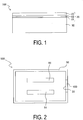
- an optical member 100 of the present embodiment includes a substrate 10 and a protective film 20 formed on the substrate 10.
- the protective film 20 includes a high refractive index layer 21 formed on the substrate 10, a low refractive index layer 22 formed on the high refractive index layer 21, and a Cu-proof protective layer 23 formed on the low refractive index layer 22, in this order from a side closer to the substrate 10.
- the substrate 10 can be formed from a desired light transmissive material.
- the light transmissive material include sapphire (aluminum oxide, Al 2 O 3 ), magnesium fluoride (MgF 2 ), calcium fluoride (CaF 2 ), amorphous silica (amorphous SiO 2 ), and crystalline silica (crystal).
- the high refractive index layer 21 of the protective film 20 has a refractive index higher than that of the substrate 10, and is formed between the substrate 10 and the low refractive index layer 22, described hereinafter, in order to allow a greater amount of incident light transmitted through the low refractive index layer 22 to enter the substrate 10.
- the high refractive index layer 21 can be formed with a sputtering method or the like.
- the high refractive index layer 21 may be omitted.
- the low refractive index layer 22 of the protective film 20 has a refractive index lower than that of the substrate 10, and is formed between the Cu-proof protective layer 23, described hereinafter, and the high refractive index layer 21, in order to allow a greater amount of incident light transmitted through the Cu-proof protective layer 23 to enter the substrate 10.
- the low refractive index layer 22 can be formed with a sputtering method or the like.
- the Cu-proof protective layer 23 is formed as a surface layer of the protective film 20 to protect the optical member 100 against copper (Cu) flying toward the optical member 100.
- the Cu-proof protective layer 23 can be formed from, for example, HfO 2 , Al 2 O 3 , Ta 2 O 5 , MgO, or a mixture thereof.
- the Cu-proof protective layer 23 can be formed with a sputtering method or the like.
- the XeCl excimer laser light source device 500 mainly includes a chamber 50 and a pair of electrodes 51 disposed in the chamber 50.
- the optical member 100 of the present embodiment can be used as a light transmitting window for allowing excimer laser light generated between the electrodes 51 to go outside the chamber 50.
- the optical member 100 is attached to a portion of the chamber 50 with the protective film 20 facing the interior of the chamber 50, as illustrated in FIG. 2 .
- Sapphire, MgF 2 , CaF 2 , amorphous silica, and crystal listed above as examples of the material of the substrate 10, HfO 2 and the like listed as examples of the materials of the high refractive index layer 21 and the Cu-proof protective layer 23, and SiO 2 and the like listed above as examples of the material of the low refractive index layer 22 all ideally transmit XeCl excimer laser light having an emission wavelength (oscillation wavelength) of 308 nm. It is thus preferable to use these materials even when the optical member 100 is used as the light transmitting window of the excimer laser light source device 500.
- the excimer laser light source device 500 including the optical member 100 of the present embodiment can be used as light sources for various uses, such as a laser annealing device, laser ablation, a laser knife, and an exposure device.
- a gas mixture containing Xe, HCl, and the like is sealed in the chamber 50.
- the XeCl excimer laser light source device 500 When the XeCl excimer laser light source device 500 operates, a large voltage difference is applied between the electrodes 51. This operation allows Xe atoms and excited Cl atoms to form excimers, and the excimers radiate laser light having a wavelength of 308 nm.
- the laser light generated in the chamber is transmitted through the optical member 100 and goes outside the chamber 50.
- the electrodes 51 of the XeCl excimer laser light source device 500 typically contain copper (Cu).
- Cu copper
- the inventor of the present invention examined fogging of the light transmitting window of the chamber and found that some fogging was not removed even by wiping. It was found by this finding that Cu was not only attached to the surface but also entered inside from the surface.
- the protective film 20 including the Cu-proof protective layer 23 as the surface layer is formed on the surface, facing the interior of the chamber 50, of the optical member 100. This configuration prevents the light transmitting window (optical member 100) from being contaminated because of entering of Cu, in the XeCl excimer laser light source device 500.
- the protective film 20 of the optical member 100 is used in such a severe environment that the protective film 20 is exposed to the gas mixture containing HCl and the like and laser light.
- the Cu-proof protective layer being the surface layer of the protective film 20 desirably has high chemical stability and a solubility of 10 ppm or less in pure water at 20°C.
- optical member 100 will be described below using Examples. However, the present invention is not limited to these Examples. Note that a sputtering method is used for film formation in all of Examples and Comparative Examples below.
- a disk made from sapphire and having a diameter of 60 mm and a thickness of 5 mm was used as a substrate.
- the c-plane of the sapphire was parallel to the circular plane having a diameter of 60 mm.
- the substrate had an internal transmittance of 99.9% or greater for light having a wavelength of 308 nm.
- a SiO 2 layer having a film thickness d of 0.052 ⁇ m was formed on the sapphire substrate, as a low refractive index layer.
- a HfO 2 layer having a film thickness d of 0.038 ⁇ m was formed on the SiO 2 layer, as a Cu-proof protective layer.
- the transmittance of the optical member of Example 1 for light having a wavelength 308 nm was calculated through simulation to be 76.8%.
- An optical member of Example 2 had the same configuration as that of the optical member of Example 1, except for a HfO 2 layer formed as a Cu-proof protective layer, that had a thickness of 0.075 ⁇ m.
- the transmittance of the optical member of Example 2 for light having a wavelength of 308 nm was calculated through simulation to be 96.2%.
- An optical member of Example 3 had the same configuration as that of the optical member of Example 1, except for a HfO 2 layer provided as a high refractive index layer between the substrate and the low refractive index layer.
- the SiO 2 layer being the low refractive index layer and the HfO 2 layer being the Cu-proof protective layer were formed. Note that both the surface layer and the layer formed between the substrate and the low refractive index layer were HfO 2 layers in Example 3, and the HfO 2 layer being the surface layer is referred to as Cu-proof protective layer and the HfO 2 layer formed between the substrate and the low refractive index layer is referred to as high refractive index layer. This also applies to Examples 4 to 6, described hereinafter.
- the transmittance of the optical member of Example 3 for light having a wavelength of 308 nm was calculated through simulation to be 64.4%.
- An optical member of Example 4 had the same configuration as that of the optical member of Example 3, except for a HfO 2 layer formed as a Cu-proof protective layer, that had a thickness of 0.075 ⁇ m.
- the transmittance of the optical member of Example 4 for light having a wavelength of 308 nm was calculated through simulation to be 99.9%.
- An optical member of Example 5 had the same configuration as that of the optical member of Example 3, except for a SiO 2 layer formed as a low refractive index layer, that had a thickness of 0.104 ⁇ m.
- the transmittance of the optical member of Example 5 for light having a wavelength of 308 nm was calculated through simulation to be 88.0%.
- An optical member of Example 6 had the same configuration as that of the optical member of Example 3, except for a HfO 2 layer formed as a high refractive index layer, that had a thickness of 0.075 ⁇ m.
- the transmittance of the optical member of Example 6 for light having a wavelength of 308 nm was calculated through simulation to be 64.4%.
- the table in FIG. 3 shows the summary of the optical members of Examples 1 to 6, with respect to the configurations thereof, the refractive indices and film thicknesses of the layers of the protective films, the refractive indices of the substrates, and the transmittance of the optical members.
- An optical member of Comparative Example 1 was prepared by forming the HfO 2 layer and the SiO 2 layer on the substrate in the same manner as those of Examples 3 and 4, except that no HfO 2 layer was provided as a Cu-proof protective layer..
- the transmittance of the optical member of Comparative Example 1 for light having a wavelength of 308 nm was calculated through simulation to be 99.9%.
- An optical member of Comparative Example 2 was prepared by laminating a SiO 2 layer, a HfO 2 layer, and a SiO 2 layer in this order from the substrate side, which was opposite to the optical members of Examples 3 to 6 prepared by laminating the HfO 2 layer, the SiO 2 layer, and the HfO 2 layer in this order from the substrate side.
- the SiO 2 layers each had a thickness of 0.052 ⁇ m, and the HfO 2 layer had a thickness of 0.038 ⁇ m.
- the transmittance of the optical member of Comparative Example 2 for light having a wavelength of 308 nm was calculated through simulation to be 98.4%.
- the table in FIG. 4 shows the summary of the optical members of Comparative Examples 1 and 2, with respect to the configurations thereof, the refractive indices and film thicknesses of the layers of the films, the refractive indices of the substrates, and the transmittance of the optical members.
- the following Cu attachment test for the optical members of Examples 1 to 6 and the optical members of Comparative Examples 1 and 2 was conducted to check resistance to Cu particles flying from the electrodes 51 and the like. Note that the resistance of the optical members of Examples 1 to 6 to flying Cu particles is mainly equal to resistance of the HfO 2 layers being the surface layers (Cu-proof protective layers) to Cu particles.
- a sample S1 in which a HfO 2 film having a film thickness d of 0.075 ⁇ m was formed on the surface of a SiO 2 substrate was used as a typified optical member of the optical members of Examples 1 to 6.
- sample S2 in which a SiO 2 film having a film thickness d of 0.052 ⁇ m was formed on the surface of a SiO 2 substrate was used as a typified optical member of the optical members of Comparative Examples 1 and 2.
- the Cu attachment test was also conducted for a SiO 2 substrate with no film formed on its surface (sample S3).
- a test device 700 used in the Cu attachment test includes a quartz chamber 70 provided with a light transmitting window 74, a condensing lens 71 disposed in the chamber 70 and concentrating light entering from the light transmitting window 74, and a copper plate 72 disposed in the chamber 70 and arranged in the focal position of the condensing lens 71 while facing the condensing lens 71.
- the chamber 70 includes an opening 75 for creating a vacuum in the chamber 70.
- the Cu attachment test was conducted using the following procedure. First, the sample S1 was placed between the condensing lens 71 and the copper plate 72 as illustrated in FIG. 5 . At this time, the sample S1 was placed substantially parallel to the condensing lens 71 and the copper plate 72, and the HfO 2 film faced the copper plate 72. The distance between the sample S1 and the copper plate 72 was approximately 6 cm.
- XeCl excimer laser light EL having a repetition frequency of 100 Hz and a radiation power of 100 mJ was radiated through the light transmitting window 74.
- the XeCl excimer laser light EL was radiated for 600 seconds.
- the beam size at the sample S1 was 2 cm ⁇ 0.5 cm
- the radiation fluence at the sample S was 100 mJ/cm 2
- the beam size at the copper plate 72 was approximately 2 mm ⁇ 1 mm
- the radiation fluence at the copper plate 72 was 5 J/cm 2 .
- the sample S1 was taken out of the test device 700, and powder attached to its surface was wiped out. The same steps were taken to radiate XeCl excimer laser light EL toward the sample S2 and the sample S3.
- Table 1 below shows a difference in transmittance calculated for each of the sample S1, the sample S2, and the sample S3.
- the transmittance of the sample S1 changed little between before and after the radiation of the XeCl excimer laser light EL.
- the transmittance of the samples S2, S3 after the radiation of the XeCl excimer laser light EL deteriorated by approximately 4% in comparison with before the radiation. It is considered that this was caused by a chemical reaction between Cu particles and the SiO 2 film or the SiO 2 substrate as described above.
- FIG. 6 is a graph of the analysis results.
- the horizontal axis indicates depth (nm) from a sample surface, and the vertical axis indicates Cu intensity (corresponding to the amount of Cu) in an arbitrary unit.
- the solid line indicates the analysis result of the sample S1
- the dotted line indicates the analysis result of the sample S2
- the dashed-dotted line indicates the analysis result of the sample S3.
- a material, such as HfO 2 , that is more difficult for Cu to enter than SiO 2 is, that is, a material having a Cu diffusion coefficient smaller than that of SiO 2 is suitable for forming the "Cu-proof protective layer" of the present invention, and a material having a Cu diffusion coefficient at 200°C that is 1/10 or less of that of SiO 2 at 200°C is more suitable for forming the "Cu-proof protective layer" of the present invention.
- the temperature of the optical member 100 of the present embodiment used as a window member of the light source device 500 of the present embodiment, during the use of light source device 500, is approximately 200°C.
- the Cu diffusion coefficient D of SiO 2 at 200°C is 1.03 ⁇ 10 -16 cm 2 /s.
- the Cu diffusion coefficient of a material suitable for forming the Cu-proof protective layer, at 200°C is desirably smaller than 1 ⁇ 10 -17 cm 2 /s.
- optical members of Examples 1 to 6 including a HfO 2 layer as the Cu-proof protective layer being the surface layer are more difficult to react with Cu particles and have higher Cu resistance than the optical members of Comparative Examples 1 and 2 including a SiO 2 layer being the surface layer.
- FIG. 7 shows change in reflectance with respect to the wavelength of incident light
- FIG. 8 shows change in transmittance with respect to the wavelength of incident light. Reflectance was measured with a micro-spectrophotometer USPM-RUIII or N&k Analyzer 1280 (n&k Technology), and transmittance was measured with CARY-5000.
- the solid line indicates a graph of the optical member of Example 4
- the dotted line indicates a graph of the optical member of Comparative Example 1.
- the optical member of Example 4 had the lowest reflectance of approximately 0.7% at a wavelength of around 308 nm.
- the reflectance was 1% or less in a wavelength region of approximately 296 to 310 nm.
- the protective film of the optical member of Example 4 offers sufficiently high performance as an anti-reflection film in addition to a protective film, against incident light having a wavelength of approximately 308 nm.
- the optical member of Comparative Example 1 had a reflectance of 1% or less in a wider wavelength region of approximately 280 nm to approximately 350 nm.
- the optical member of Example 4 had the highest transmittance of 99% or greater at a wavelength of around 308 nm.
- the transmittance was 90% or greater in a wavelength region of approximately 280 nm to 330 nm.
- the protective film of the optical member of Example 4 offers sufficiently high performance as an anti-reflection film in addition to a protective film, against incident light having a wavelength of approximately 308 nm.
- the optical member of Comparative Example 1 had a transmittance of 90% or greater in a wider wavelength region of approximately 250 nm to 400 nm or greater.
- the optical member of Example 4 has ideal anti-reflection characteristics similar to the optical member of Comparative Example 1.
- the above-described results of the Cu attachment test clearly demonstrate that when the optical member of Comparative Example 1 is used in such an environment that Cu particles may fly to the optical member, the transmittance of the optical member decreases significantly because of a reaction with Cu particles.
- the window needs to be replaced frequently.
- the optical member of Example 4 has ideal anti-reflection characteristics and is difficult to decrease its transmittance even in a case where Cu flies to the optical member, and can thus be used as a long-life window member of a chamber of a XeCl excimer laser light source device.
- FIGS. 7 and 8 also show reflectance and transmittance of an optical member of Example 7.
- the optical member of Example 7 had the same configuration as that of the optical member of Example 4, except for a Cu-proof protective layer formed from Ta 2 O 5 instead of HfO 2 .
- the optical member of Example 7 had the lowest reflectance of approximately 0.2% at a wavelength of around 308 nm and a reflectance of 1% or less in a wavelength region of approximately 296 to 312 nm. This optical member had the highest transmittance of 99% or greater at a wavelength of around 308 nm and a reflectance of 90% or greater in a wavelength region of approximately 290 nm to 320 nm. This indicates that the protective film of the optical member of Example 7 offers sufficiently high performance as an anti-reflection film in addition to a protective film, against incident light having a wavelength of 308 nm.
- Equation (5) provides (1 - n s ) 2 /(1 + n s ) 2 .
- a multilayer film in which a second layer having a refractive index n 2 and a film thickness d 2 is formed on a first layer having a refractive index n 1 and a film thickness d 1 as illustrated in FIG. 9C will be examined.
- M 1 is the characteristics matrix of the first layer
- M 2 is the characteristics matrix of the second layer.
- the optical member of Example 4 had the same film configuration as that of the optical member of Comparative Example 1, except for the HfO 2 layer as the Cu-proof protective layer being the surface layer.
- the optical member of Example 7 had the same film configuration as that of the optical member of Comparative Example 1, except for the Ta 2 O 5 layer as the Cu-proof protective layer being the surface layer.
- the protective films of the optical members of Examples 4 and 7 have reflectance equivalent to that of the optical member of Comparative Example 1 for incident light having a wavelength of 308 nm, and in other words, also function as an ideal anti-reflection film against light having a wavelength of 308 nm.
- the optical member 100 of the aforementioned embodiment includes the Cu-proof protective layer 23 as the surface layer, so that even in a case where Cu particles fly to the optical member from a surrounding environment, diffusion of Cu particles in the Cu-proof protective layer 23 is reduced.
- the optical member 100 of the present embodiment can thus be used for a long period while preventing a decrease in transmittance even in such an environment that Cu particles fly to the optical member.
- the optical member 100 of the present embodiment includes the Cu-proof protective layer 23 as the surface layer, made from a material that is chemically stable toward chlorine gas, that prevents Cu particles from entering by diffusion, and that efficiently transmits light having a wavelength of 308 nm.
- the optical member 100 of the present embodiment can thus be used suitably as the light transmitting window of the chamber of the XeCl excimer laser light source device.
- the optical member 100 of the present embodiment prevents a decrease in transmittance in such an environment that Cu particles or the like fly to the optical member.
- the chamber 50 and the light source device 500 of the present embodiment include, as the light transmitting window, the optical member 100 preventing a decrease in transmittance in such an environment that Cu particles or the like fly to the optical member, so that the frequency of maintenance can be reduced.
- an optical thin film having sufficiently small reflectance for incident light having a desired wavelength ⁇ and forming the Cu-proof protective layer 23 having a film thickness d satisfying the condition nd ⁇ /2, on the optical thin film as the surface layer, an optical thin film that can be used as an anti-reflection film for the desired wavelength ⁇ and functions as a protective film for flying Cu particles can be achieved.
- an optical thin film having both Cu resistance and anti-reflection characteristics can be formed.
- Such an optical thin film has a reflectance of 1% or less for light in a wide wavelength region of approximately 296 to 310 nm and a transmittance of 90% or greater for light in a wide wavelength region of approximately 280 nm to 330 nm.
- the film thickness or the like changes the performance of the protective film a little, low reflectance and high transmittance can be maintained for incident light having a wavelength of 308 nm.
- the protective film 20 of the aforementioned embodiment may have four or more layers.
- underlying layers of the Cu-proof protective layer 23 include high refractive index layers having a refractive index higher than that of a substrate and low refractive index layers having a refractive index lower than that of the substrate, and that the high refractive index layers and the low refractive index layers are alternately formed.
Landscapes
- Physics & Mathematics (AREA)
- Optics & Photonics (AREA)
- Electromagnetism (AREA)
- General Physics & Mathematics (AREA)
- Engineering & Computer Science (AREA)
- Plasma & Fusion (AREA)
- Chemical & Material Sciences (AREA)
- Inorganic Chemistry (AREA)
- Condensed Matter Physics & Semiconductors (AREA)
- Surface Treatment Of Optical Elements (AREA)
- Life Sciences & Earth Sciences (AREA)
- Chemical Kinetics & Catalysis (AREA)
- General Chemical & Material Sciences (AREA)
- Geochemistry & Mineralogy (AREA)
- Materials Engineering (AREA)
- Organic Chemistry (AREA)
- Exposure And Positioning Against Photoresist Photosensitive Materials (AREA)
- Lasers (AREA)
Abstract
Description
- The present invention relates to an optical member including a protective film against copper (Cu), a chamber including the optical member, and a light source device including the chamber.
- Excimer lasers that generate pulses with light radiated from excimers formed from halogen atoms and excited noble gas atoms are widely used in the semiconductor manufacturing field, medical field, and the like. In the excimer lasers, XeCl excimer lasers that use xenon (Xe) as a noble gas and chlorine (Cl) as a halogen are used as light sources of excimer laser annealing devices and the like (Patent Document 1).
- A XeCl excimer laser light source device mainly includes a chamber including a light transmitting window, and electrodes disposed in the chamber. A gas mixture containing xenon (Xe), hydrogen chloride (HCl), and the like is sealed in the chamber. When the XeCl excimer laser light source device operates, a large voltage difference is applied between the electrodes. This operation allows Xe atoms and excited Cl atoms to form excimers, and light radiated from the excimers is emitted outside through the light transmitting window of the chamber.
- The electrodes in the chamber of the excimer laser light source device are made from W and/or Cu. It is reported that these materials are partially scattered by electrical discharge and thus cause fogging of the light transmitting window (Non Patent Document 1).
- Patent Document 1:
JP 2004-39660 A -
- Non Patent Document 1: Applied Physics B63, PP229-235 (1996)
- Non Patent Document 2: Jpn. J, Appl. Phys. Vol. 38 (1999) pp. 5792-5795
- A first aspect of the present invention provides an optical member including: a substrate; and a Cu-proof protective layer formed on or above the substrate.
- A second aspect of the present invention provides an optical member including: a substrate; and a transmitting film including: a low refractive index layer having a refractive index lower than that of the substrate; and a surface layer composed of any one of Al2O3, Ta2O5, MgO, and HfO2 or a mixture of any two or more of Al2O3, Ta2O5, MgO, and HfO2.
- A third aspect of the present invention provides an optical member including: a substrate; and a multilayer film including a plurality of layers having mutually different refractive indices. The multilayer film includes a surface layer being a Cu-proof protective layer. The Cu-proof protective layer has a Cu diffusion coefficient at 200°C that is 1/10 or less of a Cu diffusion coefficient of SiO2 at 200°C.
- A fourth aspect of the present invention provides an optical member including: a substrate; and a multilayer film including a plurality of layers having mutually different refractive indices. The multilayer film includes a surface layer being a Cu-proof protective layer. The Cu-proof protective layer has a Cu diffusion coefficient at 200°C that is smaller than 1 × 10-17 cm2/s. The optical member transmits 90% or greater of vertically incident light having a wavelength of 308 nm.
- A fifth aspect of the present invention provides a chamber in which chlorine gas is sealed, the chamber including: a light transmitting window formed in the chamber. The light transmitting window is made of the optical member of any one of the first to fourth aspects.
- A sixth aspect of the present invention provides a light source device including: the chamber of the fifth aspect; and an electrode disposed in the chamber and containing Cu.
- A seventh aspect of the present invention provides a light transmitting window for an excimer laser light source device, the light transmitting window being made of the optical member of any one of the first to fourth aspects.
-
-
FIG. 1 is a schematic cross-sectional view illustrating a configuration of an optical member according to an embodiment of the present invention. -
FIG. 2 is a schematic cross-sectional view illustrating a configuration of a light source device according to the embodiment of the present invention. -
FIG. 3 is a table showing configurations, transmittance, and the like of optical members of Examples 1 to 6 of the present invention. -
FIG. 4 is a table showing configurations, transmittance, and the like of optical members of Comparative Examples 1 and 2. -
FIG. 5 is an explanatory diagram illustrating a general configuration of a test device for testing Cu resistance of an optical member. -
FIG. 6 is a graph showing the amount of Cu diffused in optical members. -
FIG. 7 is a graph showing change in reflectance with respect to the wavelength of incident light, of each of the optical members of Examples 4 and 7 and the optical member of Comparative Example 1. -
FIG. 8 is a graph showing change in transmittance with respect to the wavelength of incident light, of each of the optical members of Examples 4 and 7 and the optical member of Comparative Example 1. -
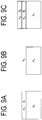
FIGS. 9A, 9B, and 9C are explanatory diagrams illustrating the role of a surface layer having a film thickness d satisfying the condition nd = λ/2 with respect to incident light having a wavelength λ. - In the present embodiment, a Cu-proof protective layer is provided as a surface layer (outermost layer or upper most layer) of an optical member. In the present specification, "Cu-proof protective layer" refers to a layer formed from a material that is difficult for Cu to enter. A material that is difficult for Cu to enter specifically refers to a material having a structure that is difficult for a univalent cation, such as Na+, to enter. It tends to be difficult for Cu to enter a material having such a structure. One example of such a material that is difficult for Cu to enter is a material having a Cu diffusion coefficient (diffusion rate) at 200°C smaller than those of other materials (such as SiO2). A layer formed from such a material functions as a Cu-proof protective layer. The diffusion coefficient (diffusion rate) can be measured with a generally used measuring method, for example, a dipping method. Examples of specific materials that have been found by the inventor of the present invention to be excellent for forming a Cu-proof protective layer include the aforementioned HfO2, Al2O3, Ta2O5, and MgO.
- A low refractive index layer having a refractive index lower than that of a substrate may be provided between the substrate and the Cu-proof protective layer. The low refractive index layer increases a difference in the refractive index between the layers, resulting in improvement in anti-reflection effect. Furthermore, by providing a high refractive index layer having a refractive index higher than that of the substrate between the substrate and the low refractive index layer, anti-reflection effect can be further improved.
- Embodiments for carrying out the present invention will be described in detail below with reference to the drawings. Herein, an example in which a high refractive index layer and a low refractive index layer are provided between a substrate and a Cu-proof protective layer is described. As illustrated in
FIG. 1 , anoptical member 100 of the present embodiment includes asubstrate 10 and aprotective film 20 formed on thesubstrate 10. Theprotective film 20 includes a highrefractive index layer 21 formed on thesubstrate 10, a lowrefractive index layer 22 formed on the highrefractive index layer 21, and a Cu-proofprotective layer 23 formed on the lowrefractive index layer 22, in this order from a side closer to thesubstrate 10. - The
substrate 10 can be formed from a desired light transmissive material. Examples of the light transmissive material include sapphire (aluminum oxide, Al2O3), magnesium fluoride (MgF2), calcium fluoride (CaF2), amorphous silica (amorphous SiO2), and crystalline silica (crystal). - The high
refractive index layer 21 of theprotective film 20 has a refractive index higher than that of thesubstrate 10, and is formed between thesubstrate 10 and the lowrefractive index layer 22, described hereinafter, in order to allow a greater amount of incident light transmitted through the lowrefractive index layer 22 to enter thesubstrate 10. - In a case where the
substrate 10 is formed from sapphire (having a refractive index of 1.811 (λ = 308 nm)), for example, the highrefractive index layer 21 can be formed from an oxide, such as HfO2 (having a refractive index of 2.053 (λ = 308 nm)), Ta2O5 (having a refractive index of 2.277 (λ = 308 nm)), and MgO (having a refractive index of 1.791 (λ = 308 nm)). - The high
refractive index layer 21 can be formed with a sputtering method or the like. The highrefractive index layer 21 preferably has a film thickness d21 of approximately 30 to 60 nm, and more preferably approximately 30 nm to 50 nm. Even more preferably, the film thickness d21 of the highrefractive index layer 21 satisfies the condition n21d21 = λ/4, where n21 is a refractive index of the material forming the highrefractive index layer 21 and λ is a wavelength of light entering theoptical member 100. By setting such a thickness, light reflected off the surface of the highrefractive index layer 21 and light transmitted through the highrefractive index layer 21 and reflected off the surface of thesubstrate 10 cancel out each other by interference, so that ideal anti-reflection effect is yielded. Note that the highrefractive index layer 21 may be omitted. - The low
refractive index layer 22 of theprotective film 20 has a refractive index lower than that of thesubstrate 10, and is formed between the Cu-proofprotective layer 23, described hereinafter, and the highrefractive index layer 21, in order to allow a greater amount of incident light transmitted through the Cu-proofprotective layer 23 to enter thesubstrate 10. - In a case where the
substrate 10 is formed from sapphire (having a refractive index of 1.811 (λ = 308 nm)), for example, the lowrefractive index layer 22 can be formed from SiO2 (having a refractive index of 1.486 (λ = 308 nm)), MgF2 (having a refractive index of 1.399 (λ = 308 nm)), CaF2 (having a refractive index of 1.452 (λ = 308 nm)), or the like. - The low
refractive index layer 22 can be formed with a sputtering method or the like. The lowrefractive index layer 22 preferably has a film thickness d22 of approximately 30 to 60 nm, and more preferably approximately 50 nm to 60 nm. Even more preferably, the film thickness d22 of the lowrefractive index layer 22 satisfies the condition n22d22 = λ/4, where n22 is a refractive index of the material forming the lowrefractive index layer 22 and λ is a wavelength of light entering theoptical member 100. By setting such a thickness, light reflected off the surface of the lowrefractive index layer 22 and light transmitted through the lowrefractive index layer 22 and reflected off the surface of the highrefractive index layer 21 cancel out each other by interference, so that ideal anti-reflection effect is yielded. - The Cu-proof
protective layer 23 is formed as a surface layer of theprotective film 20 to protect theoptical member 100 against copper (Cu) flying toward theoptical member 100. The Cu-proofprotective layer 23 can be formed from, for example, HfO2, Al2O3, Ta2O5, MgO, or a mixture thereof. - The Cu-proof
protective layer 23 can be formed with a sputtering method or the like. The Cu-proofprotective layer 23 preferably has a film thickness d23 of approximately 60 to 120 nm, and more preferably approximately 60 nm to 90 nm. Even more preferably, the film thickness d23 of the Cu-proofprotective layer 23 satisfies the condition n23d23 = λ/2 as described below, where n23 is a refractive index of the material forming theprotective layer 23 and λ is a wavelength of light entering theoptical member 100. - Next, a case of using the
optical member 100 of the present embodiment for a XeCl excimer laserlight source device 500 will be described. - As illustrated in
FIG. 2 , the XeCl excimer laserlight source device 500 mainly includes achamber 50 and a pair ofelectrodes 51 disposed in thechamber 50. In the XeCl excimer laserlight source device 500 having this configuration, theoptical member 100 of the present embodiment can be used as a light transmitting window for allowing excimer laser light generated between theelectrodes 51 to go outside thechamber 50. - Specifically, the
optical member 100 is attached to a portion of thechamber 50 with theprotective film 20 facing the interior of thechamber 50, as illustrated inFIG. 2 . Sapphire, MgF2, CaF2, amorphous silica, and crystal listed above as examples of the material of thesubstrate 10, HfO2 and the like listed as examples of the materials of the highrefractive index layer 21 and the Cu-proofprotective layer 23, and SiO2 and the like listed above as examples of the material of the lowrefractive index layer 22 all ideally transmit XeCl excimer laser light having an emission wavelength (oscillation wavelength) of 308 nm. It is thus preferable to use these materials even when theoptical member 100 is used as the light transmitting window of the excimer laserlight source device 500. - The excimer laser
light source device 500 including theoptical member 100 of the present embodiment can be used as light sources for various uses, such as a laser annealing device, laser ablation, a laser knife, and an exposure device. - A gas mixture containing Xe, HCl, and the like is sealed in the
chamber 50. When the XeCl excimer laserlight source device 500 operates, a large voltage difference is applied between theelectrodes 51. This operation allows Xe atoms and excited Cl atoms to form excimers, and the excimers radiate laser light having a wavelength of 308 nm. The laser light generated in the chamber is transmitted through theoptical member 100 and goes outside thechamber 50. - The
electrodes 51 of the XeCl excimer laserlight source device 500 typically contain copper (Cu). When a large voltage difference is applied between theelectrodes 51 to generate excimer laser light, Cu contained in theelectrodes 51 is scattered around. The inventor of the present invention examined fogging of the light transmitting window of the chamber and found that some fogging was not removed even by wiping. It was found by this finding that Cu was not only attached to the surface but also entered inside from the surface. - Here, in the XeCl excimer laser
light source device 500 including theoptical member 100 of the present embodiment as the light transmitting window, theprotective film 20 including the Cu-proofprotective layer 23 as the surface layer is formed on the surface, facing the interior of thechamber 50, of theoptical member 100. This configuration prevents the light transmitting window (optical member 100) from being contaminated because of entering of Cu, in the XeCl excimer laserlight source device 500. - In this way, the
protective film 20 of theoptical member 100 is used in such a severe environment that theprotective film 20 is exposed to the gas mixture containing HCl and the like and laser light. Thus, the Cu-proof protective layer being the surface layer of theprotective film 20 desirably has high chemical stability and a solubility of 10 ppm or less in pure water at 20°C. - The
optical member 100 will be described below using Examples. However, the present invention is not limited to these Examples. Note that a sputtering method is used for film formation in all of Examples and Comparative Examples below. - A disk made from sapphire and having a diameter of 60 mm and a thickness of 5 mm was used as a substrate. The c-plane of the sapphire was parallel to the circular plane having a diameter of 60 mm. The substrate had an internal transmittance of 99.9% or greater for light having a wavelength of 308 nm.
- A SiO2 layer having a film thickness d of 0.052 µm was formed on the sapphire substrate, as a low refractive index layer. This film thickness d substantially satisfied the condition nd = λ/4, where n = 1.486 and λ = 308 nm. Then, a HfO2 layer having a film thickness d of 0.038 µm was formed on the SiO2 layer, as a Cu-proof protective layer. This film thickness d substantially satisfied the condition nd = λ/4, where n = 2.053 and λ = 308 nm.
- The transmittance of the optical member of Example 1 for light having a wavelength 308 nm was calculated through simulation to be 76.8%.
- An optical member of Example 2 had the same configuration as that of the optical member of Example 1, except for a HfO2 layer formed as a Cu-proof protective layer, that had a thickness of 0.075 µm. The film thickness d of the HfO2 layer being the Cu-proof protective layer substantially satisfied the condition nd = λ/2, where n = 2.053 and λ = 308 nm.
- The transmittance of the optical member of Example 2 for light having a wavelength of 308 nm was calculated through simulation to be 96.2%.
- An optical member of Example 3 had the same configuration as that of the optical member of Example 1, except for a HfO2 layer provided as a high refractive index layer between the substrate and the low refractive index layer.
- The HfO2 layer having a film thickness d of 0.038 µm was formed as the high refractive index layer on the substrate. This film thickness d substantially satisfied the condition nd = λ/4, where n = 2.053 and λ = 308 nm. On this HfO2 layer, the SiO2 layer being the low refractive index layer and the HfO2 layer being the Cu-proof protective layer were formed. Note that both the surface layer and the layer formed between the substrate and the low refractive index layer were HfO2 layers in Example 3, and the HfO2 layer being the surface layer is referred to as Cu-proof protective layer and the HfO2 layer formed between the substrate and the low refractive index layer is referred to as high refractive index layer. This also applies to Examples 4 to 6, described hereinafter.
- The transmittance of the optical member of Example 3 for light having a wavelength of 308 nm was calculated through simulation to be 64.4%.
- An optical member of Example 4 had the same configuration as that of the optical member of Example 3, except for a HfO2 layer formed as a Cu-proof protective layer, that had a thickness of 0.075 µm. The film thickness d of the HfO2 layer being the Cu-proof protective layer substantially satisfied the condition nd = λ/2, where n = 2.053 and λ = 308 nm.
- The transmittance of the optical member of Example 4 for light having a wavelength of 308 nm was calculated through simulation to be 99.9%.
- An optical member of Example 5 had the same configuration as that of the optical member of Example 3, except for a SiO2 layer formed as a low refractive index layer, that had a thickness of 0.104 µm. The film thickness d of the SiO2 layer formed as the low refractive index layer substantially satisfied the condition nd = λ/2, where n = 1.486 and λ = 308 nm.
- The transmittance of the optical member of Example 5 for light having a wavelength of 308 nm was calculated through simulation to be 88.0%.
- An optical member of Example 6 had the same configuration as that of the optical member of Example 3, except for a HfO2 layer formed as a high refractive index layer, that had a thickness of 0.075 µm. The film thickness d of the HfO2 layer formed as the high refractive index layer substantially satisfied the condition nd = λ/2, where n = 2.053 and λ = 308 nm.
- The transmittance of the optical member of Example 6 for light having a wavelength of 308 nm was calculated through simulation to be 64.4%.
- The table in
FIG. 3 shows the summary of the optical members of Examples 1 to 6, with respect to the configurations thereof, the refractive indices and film thicknesses of the layers of the protective films, the refractive indices of the substrates, and the transmittance of the optical members. - An optical member of Comparative Example 1 was prepared by forming the HfO2 layer and the SiO2 layer on the substrate in the same manner as those of Examples 3 and 4, except that no HfO2 layer was provided as a Cu-proof protective layer.. The transmittance of the optical member of Comparative Example 1 for light having a wavelength of 308 nm was calculated through simulation to be 99.9%.
- An optical member of Comparative Example 2 was prepared by laminating a SiO2 layer, a HfO2 layer, and a SiO2 layer in this order from the substrate side, which was opposite to the optical members of Examples 3 to 6 prepared by laminating the HfO2 layer, the SiO2 layer, and the HfO2 layer in this order from the substrate side. The SiO2 layers each had a thickness of 0.052 µm, and the HfO2 layer had a thickness of 0.038 µm.
- The transmittance of the optical member of Comparative Example 2 for light having a wavelength of 308 nm was calculated through simulation to be 98.4%.
- The table in
FIG. 4 shows the summary of the optical members of Comparative Examples 1 and 2, with respect to the configurations thereof, the refractive indices and film thicknesses of the layers of the films, the refractive indices of the substrates, and the transmittance of the optical members. - The following Cu attachment test for the optical members of Examples 1 to 6 and the optical members of Comparative Examples 1 and 2 was conducted to check resistance to Cu particles flying from the
electrodes 51 and the like. Note that the resistance of the optical members of Examples 1 to 6 to flying Cu particles is mainly equal to resistance of the HfO2 layers being the surface layers (Cu-proof protective layers) to Cu particles. Thus, in the following Cu attachment test, a sample S1 in which a HfO2 film having a film thickness d of 0.075 µm was formed on the surface of a SiO2 substrate was used as a typified optical member of the optical members of Examples 1 to 6. For the same reason, a sample S2 in which a SiO2 film having a film thickness d of 0.052 µm was formed on the surface of a SiO2 substrate was used as a typified optical member of the optical members of Comparative Examples 1 and 2. The Cu attachment test was also conducted for a SiO2 substrate with no film formed on its surface (sample S3). - As illustrated in
FIG. 5 , atest device 700 used in the Cu attachment test includes aquartz chamber 70 provided with alight transmitting window 74, a condensinglens 71 disposed in thechamber 70 and concentrating light entering from thelight transmitting window 74, and acopper plate 72 disposed in thechamber 70 and arranged in the focal position of the condensinglens 71 while facing the condensinglens 71. Thechamber 70 includes anopening 75 for creating a vacuum in thechamber 70. - The Cu attachment test was conducted using the following procedure. First, the sample S1 was placed between the condensing
lens 71 and thecopper plate 72 as illustrated inFIG. 5 . At this time, the sample S1 was placed substantially parallel to the condensinglens 71 and thecopper plate 72, and the HfO2 film faced thecopper plate 72. The distance between the sample S1 and thecopper plate 72 was approximately 6 cm. - Next, air in the
chamber 70 was discharged through theopening 75 of thechamber 70 to create a vacuum of approximately 1 Pa in thechamber 70. Then, as illustrated inFIG. 5 , XeCl excimer laser light EL having a repetition frequency of 100 Hz and a radiation power of 100 mJ was radiated through thelight transmitting window 74. The XeCl excimer laser light EL transmitted through the condensinglens 71 and the sample S1 was then concentrated on thecopper plate 72, and Cu particles removed (emitted) from thecopper plate 72, on a principle similar to that of a laser ablation method, flew to the HfO2 film of the sample S1. The XeCl excimer laser light EL was radiated for 600 seconds. - Concerning the radiated XeCl excimer laser light EL, the beam size at the sample S1 was 2 cm × 0.5 cm, the radiation fluence at the sample S was 100 mJ/cm2, the beam size at the
copper plate 72 was approximately 2 mm × 1 mm, and the radiation fluence at thecopper plate 72 was 5 J/cm2. - After the radiation, the sample S1 was taken out of the
test device 700, and powder attached to its surface was wiped out. The same steps were taken to radiate XeCl excimer laser light EL toward the sample S2 and the sample S3. - After the radiation, (1) visual inspection of a condition of the surface, (2) measurement of a difference in transmittance (transmittance before the radiation - transmittance after the radiation), and (3) time-of-flight secondary ion mass spectrometric analysis (TOF-SIMS analysis) were performed for each of the samples S1, S2, and S3.
- Before visual inspection, dirt was wiped out with a wiping cloth with ethanol applied thereto. Then, inspection was performed. No Cu particles entering the sample S1 were observed. The sample S2 was observed to have white fogging. Cu particles attached to the sample S2 chemically reacted with the SiO2 film and could not be wiped out. The sample S3 was also observed to have white fogging. Cu particles attached to the sample S3 chemically reacted with the SiO2 substrate and could not be wiped out.
- Table 1 below shows a difference in transmittance calculated for each of the sample S1, the sample S2, and the sample S3. The transmittance of the sample S1 changed little between before and after the radiation of the XeCl excimer laser light EL. In contrast, the transmittance of the samples S2, S3 after the radiation of the XeCl excimer laser light EL deteriorated by approximately 4% in comparison with before the radiation. It is considered that this was caused by a chemical reaction between Cu particles and the SiO2 film or the SiO2 substrate as described above.
[Table 1] Sample Difference in transmittance S1 0.1 S2 3.5 S3 4.4 - TOF-SIMS analysis was performed for each of the samples S1 to S3 to check intensity of Cu entering the sample.
FIG. 6 is a graph of the analysis results. The horizontal axis indicates depth (nm) from a sample surface, and the vertical axis indicates Cu intensity (corresponding to the amount of Cu) in an arbitrary unit. InFIG. 6 , the solid line indicates the analysis result of the sample S1, the dotted line indicates the analysis result of the sample S2, and the dashed-dotted line indicates the analysis result of the sample S3. - In
FIG. 6 , a greater tilt to the lower right of the graph indicates that Cu particles are more difficult to enter. It is understood from the results that HfO2 was more difficult to react with Cu than SiO2 was, and that Cu particles were thus prevented from entering the HfO2 film of the sample S1. - As shown in
FIG. 6 , as the depth (nm) from the sample surface becomes greater, Cu intensity of HfO2 decreases more significantly than that of SiO2. A material, such as HfO2, that is more difficult for Cu to enter than SiO2 is, that is, a material having a Cu diffusion coefficient smaller than that of SiO2 is suitable for forming the "Cu-proof protective layer" of the present invention, and a material having a Cu diffusion coefficient at 200°C that is 1/10 or less of that of SiO2 at 200°C is more suitable for forming the "Cu-proof protective layer" of the present invention. The temperature of theoptical member 100 of the present embodiment used as a window member of thelight source device 500 of the present embodiment, during the use oflight source device 500, is approximately 200°C. - Note that as described in
Non Patent Document 2, the Cu diffusion coefficient D of SiO2 can be obtained by Equation (1) below:
[Equation 1]
- It is understood from the aforementioned test that the optical members of Examples 1 to 6 including a HfO2 layer as the Cu-proof protective layer being the surface layer are more difficult to react with Cu particles and have higher Cu resistance than the optical members of Comparative Examples 1 and 2 including a SiO2 layer being the surface layer.
- Next, the spectral reflectance and spectral transmittance of the optical member of Example 4 and the optical member of Comparative Example 1 were measured.
FIG. 7 shows change in reflectance with respect to the wavelength of incident light, andFIG. 8 shows change in transmittance with respect to the wavelength of incident light. Reflectance was measured with a micro-spectrophotometer USPM-RUIII or N&k Analyzer 1280 (n&k Technology), and transmittance was measured with CARY-5000. In each ofFIGS. 7 and8 , the solid line indicates a graph of the optical member of Example 4, and the dotted line indicates a graph of the optical member of Comparative Example 1. - With reference to
FIG. 7 , the optical member of Example 4 had the lowest reflectance of approximately 0.7% at a wavelength of around 308 nm. The reflectance was 1% or less in a wavelength region of approximately 296 to 310 nm. This indicates that the protective film of the optical member of Example 4 offers sufficiently high performance as an anti-reflection film in addition to a protective film, against incident light having a wavelength of approximately 308 nm. Note that the optical member of Comparative Example 1 had a reflectance of 1% or less in a wider wavelength region of approximately 280 nm to approximately 350 nm. - With reference to
FIG. 8 , the optical member of Example 4 had the highest transmittance of 99% or greater at a wavelength of around 308 nm. The transmittance was 90% or greater in a wavelength region of approximately 280 nm to 330 nm. This indicates that the protective film of the optical member of Example 4 offers sufficiently high performance as an anti-reflection film in addition to a protective film, against incident light having a wavelength of approximately 308 nm. Note that the optical member of Comparative Example 1 had a transmittance of 90% or greater in a wider wavelength region of approximately 250 nm to 400 nm or greater. - In this way, although it is shown within a relatively small wavelength region, the optical member of Example 4 has ideal anti-reflection characteristics similar to the optical member of Comparative Example 1. The above-described results of the Cu attachment test clearly demonstrate that when the optical member of Comparative Example 1 is used in such an environment that Cu particles may fly to the optical member, the transmittance of the optical member decreases significantly because of a reaction with Cu particles. Thus, when the optical member of Comparative Example 1 is used as a light transmitting window of a chamber of a XeCl excimer laser light source device, for example, the window needs to be replaced frequently. In contrast, the optical member of Example 4 has ideal anti-reflection characteristics and is difficult to decrease its transmittance even in a case where Cu flies to the optical member, and can thus be used as a long-life window member of a chamber of a XeCl excimer laser light source device.
- Note that
FIGS. 7 and8 also show reflectance and transmittance of an optical member of Example 7. The optical member of Example 7 had the same configuration as that of the optical member of Example 4, except for a Cu-proof protective layer formed from Ta2O5 instead of HfO2. The film thickness d of the Cu-proof protective layer formed from Ta2O5 was 0.068 µm and substantially satisfied the condition nd = λ/2, where n = 2.277 and λ = 308 nm. - The optical member of Example 7 had the lowest reflectance of approximately 0.2% at a wavelength of around 308 nm and a reflectance of 1% or less in a wavelength region of approximately 296 to 312 nm. This optical member had the highest transmittance of 99% or greater at a wavelength of around 308 nm and a reflectance of 90% or greater in a wavelength region of approximately 290 nm to 320 nm. This indicates that the protective film of the optical member of Example 7 offers sufficiently high performance as an anti-reflection film in addition to a protective film, against incident light having a wavelength of 308 nm.
- Like the above-described optical members of Examples 4 and 7, when the film thickness d of a Cu-proof protective layer of an optical member substantially satisfied the condition nd = λ/2 where the wavelength λ = 308 nm, the optical member exhibited ideal anti-reflection characteristics against light having a wavelength of 308 nm. The reason can be considered as described below.
- When a single-layer film having a refractive index n1 and a film thickness d1 is provided on a substrate having a refractive index ns as illustrated in
FIG. 9A , the reflectance of the single-layer film for vertically incident light having a wavelength λ is represented by Equation (2) below:
[Equation 2]
- Here, each of A, B, C, and D in Equation (2) can be obtained by obtaining δ with Equation (3) below, by applying nd = n1d1 to Equation (3), and then inserting the obtained value δ into Equation (4) (characteristics matrix) below:
[Equation 3]
[Equation 4]
- When the film thickness d1 satisfies the condition n1d1 = λ/2, Equation (3) provides δ = π, and Equation (4) provides A = - 1, B = 0, C = 0, and D = - 1. Equation (2) thus provides Reflectance R = (1 - ns)2/(1 + ns)2.
- On the other hand, when a substrate having a refractive index ns is placed in a medium having a refractive index n0 as illustrated in
FIG. 9B , Reflectance R0 of the substrate for vertically incident light can be obtained by Equation (5) below:
[Equation 5]
- Here, providing n0 = 1 because the refractive index of air is 1, Equation (5) provides (1 - ns)2/(1 + ns)2. This is equal to the reflectance of the aforementioned optical member having the single-layer film having a film thickness d1 satisfying the condition n1d1 = λ/2. That is, the reflectance for vertically incident light having a wavelength λ, of an optical member in which a single-layer film having a film thickness d1 satisfying the condition n1d1 = λ/2 is formed on a substrate is theoretically equal to the reflectance for vertically incident light having a wavelength λ, of a substrate without a single-layer film.
- Next, a multilayer film in which a second layer having a refractive index n2 and a film thickness d2 is formed on a first layer having a refractive index n1 and a film thickness d1 as illustrated in
FIG. 9C will be examined. The film thickness d1 of the first layer satisfies the condition n1d1 = λ/4, and the film thickness d2 of the second layer satisfies the condition n2d2 = λ/2. - At this time, the characteristics matrix M of the multilayer film is represented by Equation (6) below:
[Equation 6]
- Furthermore, a single-layer film obtained by removing the second layer from the multilayer film illustrated in
FIG. 9C will be examined. The characteristics matrix M1 of the first layer is represented by Equation (7) below:
[Equation 7]
- This provides A = 0, B = 1/n1, C = n1, and D = 0. Equation (2) thus provides the reflectance for vertically incident light having a wavelength λ, of the single-layer film formed by only the first layer as R = (ns - n1 2)2/(ns + n1 2)2, which is the same as the reflectance of the aforementioned multilayer film. That is, the reflectance for vertically incident light having a wavelength λ, of an optical member in which a multilayer film including a layer, as a surface layer, having a film thickness d2 satisfying the condition n2d2 = λ/2 is formed on a substrate is theoretically equal to the reflectance for vertically incident light having a wavelength λ, of an optical member in which an optical thin film obtained by removing the surface layer from the above multilayer film is formed on a substrate.
- Here, the optical member of Example 4 had the same film configuration as that of the optical member of Comparative Example 1, except for the HfO2 layer as the Cu-proof protective layer being the surface layer. Similarly, the optical member of Example 7 had the same film configuration as that of the optical member of Comparative Example 1, except for the Ta2O5 layer as the Cu-proof protective layer being the surface layer. The film thickness d of the HfO2 layer of Example 4 and the film thickness d of the Ta2O5 layer of Example 7 with respect to incident light having a wavelength λ of 308 nm satisfied the condition nd = λ/2. Thus, the protective films of the optical members of Examples 4 and 7 have reflectance equivalent to that of the optical member of Comparative Example 1 for incident light having a wavelength of 308 nm, and in other words, also function as an ideal anti-reflection film against light having a wavelength of 308 nm.
- Effects of the optical members of the aforementioned embodiment and Examples will be summarized below.
- The
optical member 100 of the aforementioned embodiment includes the Cu-proofprotective layer 23 as the surface layer, so that even in a case where Cu particles fly to the optical member from a surrounding environment, diffusion of Cu particles in the Cu-proofprotective layer 23 is reduced. Theoptical member 100 of the present embodiment can thus be used for a long period while preventing a decrease in transmittance even in such an environment that Cu particles fly to the optical member. - In the XeCl excimer laser light source device, chlorine gas is sealed in the chamber, and Cu particles fly from the electrodes. The
optical member 100 of the present embodiment includes the Cu-proofprotective layer 23 as the surface layer, made from a material that is chemically stable toward chlorine gas, that prevents Cu particles from entering by diffusion, and that efficiently transmits light having a wavelength of 308 nm. Theoptical member 100 of the present embodiment can thus be used suitably as the light transmitting window of the chamber of the XeCl excimer laser light source device. - The
optical member 100 of the present embodiment prevents a decrease in transmittance in such an environment that Cu particles or the like fly to the optical member. Thechamber 50 and thelight source device 500 of the present embodiment include, as the light transmitting window, theoptical member 100 preventing a decrease in transmittance in such an environment that Cu particles or the like fly to the optical member, so that the frequency of maintenance can be reduced. - In the
optical member 100 of the aforementioned embodiment, the film thickness d of the Cu-proofprotective layer 23 being the surface layer of theprotective film 20 with respect to incident light having a wavelength λ is set to satisfy the condition nd = λ/2, so that the reflectance of theprotective film 20 for incident light having a wavelength λ can be equivalent to a reflectance, for incident light having a wavelength λ, of the optical thin film obtained by removing the Cu-proofprotective layer 23 being the surface layer from theprotective film 20. Thus, by forming an optical thin film having sufficiently small reflectance for incident light having a desired wavelength λ and forming the Cu-proofprotective layer 23 having a film thickness d satisfying the condition nd = λ/2, on the optical thin film as the surface layer, an optical thin film that can be used as an anti-reflection film for the desired wavelength λ and functions as a protective film for flying Cu particles can be achieved. - In the
optical member 100 of the aforementioned embodiment, by setting the film thicknesses of the highrefractive index layer 21, the lowrefractive index layer 22, and the Cu-proofprotective layer 23 as those of Example 4, an optical thin film having both Cu resistance and anti-reflection characteristics can be formed. Such an optical thin film has a reflectance of 1% or less for light in a wide wavelength region of approximately 296 to 310 nm and a transmittance of 90% or greater for light in a wide wavelength region of approximately 280 nm to 330 nm. Thus, even in a case where variation in temperature, the film thickness or the like changes the performance of the protective film a little, low reflectance and high transmittance can be maintained for incident light having a wavelength of 308 nm. - Note that the
protective film 20 of the aforementioned embodiment may have four or more layers. In this case, it is desirable that underlying layers of the Cu-proofprotective layer 23 include high refractive index layers having a refractive index higher than that of a substrate and low refractive index layers having a refractive index lower than that of the substrate, and that the high refractive index layers and the low refractive index layers are alternately formed. - Provided that the features of the present invention are ensured, the present invention is not limited to the embodiments described above, and other embodiments that embody the technical concepts of the present invention are also included within the scope of the present invention.
-
- 10 Substrate
- 20 Protective film
- 21 High refractive index layer
- 22 Low refractive index layer
- 23 Cu-proof protective layer
- 50, 70 Chamber
- 51 Electrode
- 71 Condensing lens
- 72 Copper plate
- 100 Optical member
- 500 XeCl excimer laser light source device
- 700 Test device
Claims (30)
- An optical member comprising:a substrate; anda Cu-proof protective layer formed on or above the substrate.
- The optical member according to claim 1, further comprising a low refractive index layer formed between the substrate and the Cu-proof protective layer, the low refractive index layer having a refractive index lower than a refractive index of the substrate.
- The optical member according to claim 1 or 2, wherein the low refractive index layer and/or the Cu-proof protective layer functions as an anti-reflection film.
- The optical member according to claim 2 or 3, wherein the low refractive index layer is a SiO2 layer.
- The optical member according to any one of claims 1 to 4, wherein the optical member has a transmittance of 90% or greater for vertically incident light having a wavelength of 308 nm.
- An optical member comprising:a substrate; anda transmitting film comprising:a low refractive index layer having a refractive index lower than that of the substrate; anda surface layer composed of any one of Al2O3, Ta2O5, MgO, and HfO2 or a mixture of any two or more of Al2O3, Ta2O5, MgO, and HfO2.
- The optical member according to claim 6, wherein the transmitting film functions as an anti-reflection film.
- The optical member according to claim 6 or 7, wherein the low refractive index layer is a SiO2 layer.
- The optical member according to any one of claims 6 to 8, wherein the surface layer has a thickness satisfying a condition nd = λ/2, where λ is a wavelength of light entering the optical member and n is a refractive index of the surface layer.
- The optical member according to any one of claims 6 to 9, wherein the optical member has a transmittance of 90% or greater for vertically incident light having a wavelength of 308 nm.
- The optical member according to any one of claims 6 to 10, wherein the surface layer is a HfO2 layer.
- The optical member according to any one of claims 6 to 11, further comprising a high refractive index layer formed between the substrate and the low refractive index layer, the high refractive index layer having a refractive index higher than a refractive index of the substrate.
- The optical member according to claim 12, wherein the surface layer and the high refractive index layer are composed of a same material.
- An optical member comprising:a substrate; anda multilayer film comprising a plurality of layers having mutually different refractive indices;the multilayer film comprising a surface layer being a Cu-proof protective layer, andthe Cu-proof protective layer having a Cu diffusion coefficient at 200°C that is 1/10 or less of a Cu diffusion coefficient of SiO2 at 200°C.
- The optical member according to claim 14, wherein the optical member has a transmittance of 90% or greater for vertically incident light having a wavelength of 308 nm.
- An optical member comprising:a substrate; anda multilayer film comprising a plurality of layers having mutually different refractive indices;the multilayer film comprising a surface layer being a Cu-proof protective layer,the Cu-proof protective layer having a Cu diffusion coefficient at 200°C that is smaller than 1 × 10-17 cm2/s, andthe optical member transmitting 90% or greater of vertically incident light having a wavelength of 308 nm.
- The optical member according to claim 16, wherein the Cu-proof protective layer has a solubility of 10 ppm or less in pure water at 20°C.
- The optical member according to any one of claims 14 to 17, wherein the multilayer film functions as an anti-reflection film.
- The optical member according to any one of claims 14 to 18, wherein:the multilayer film further comprises a low refractive index layer having a refractive index lower than that of the substrate; andthe low refractive index layer is a SiO2 layer.
- The optical member according to any one of claims 1 to 5 and 14 to 19, wherein the Cu-proof protective layer has a thickness satisfying a condition nd = λ/2, where λ is a wavelength of light entering the optical member and n is a refractive index of the Cu-proof protective layer.
- The optical member according to any one of claims 1 to 5 and 14 to 20, wherein the Cu-proof protective layer is composed of any one of Al2O3, Ta2O5, MgO, and HfO2 or a mixture of any two or more of Al2O3, Ta2O5, MgO, and HfO2.
- The optical member according to any one of claims 1 to 5 and 14 to 21, wherein the Cu-proof protective layer is a HfO2 layer.
- The optical member according to any one of claims 1 to 5 and 19, further comprising a high refractive index layer formed between the substrate and the low refractive index layer, the high refractive index layer having a refractive index higher than a refractive index of the substrate.
- The optical member according to claim 23, wherein the Cu-proof protective layer and the high refractive index layer are composed of a same material.
- The optical member according to claim 24, wherein the Cu-proof protective layer and the high refractive index layer are HfO2 layers.
- The optical member according to any one of claims 1 to 25, wherein the substrate is an Al2O3 substrate.
- A chamber in which chlorine gas is sealed, the chamber comprising:a light transmitting window formed in the chamber;the light transmitting window being made of the optical member according to any one of claims 1 to 26.
- A light source device comprising:the chamber according to claim 27; andan electrode disposed in the chamber and containing Cu.
- The light source device according to claim 28, wherein the light source device is a XeCl excimer laser light source device.
- A light transmitting window for an excimer laser light source device, the light transmitting window being made of the optical member according to any one of claims 1 to 26.
Applications Claiming Priority (2)
| Application Number | Priority Date | Filing Date | Title |
|---|---|---|---|
| JP2015193373 | 2015-09-30 | ||
| PCT/JP2016/078183 WO2017057233A1 (en) | 2015-09-30 | 2016-09-26 | Optical member, chamber, and light source device |
Publications (2)
| Publication Number | Publication Date |
|---|---|
| EP3358377A1 true EP3358377A1 (en) | 2018-08-08 |
| EP3358377A4 EP3358377A4 (en) | 2019-05-01 |
Family
ID=58427389
Family Applications (1)
| Application Number | Title | Priority Date | Filing Date |
|---|---|---|---|
| EP16851404.0A Withdrawn EP3358377A4 (en) | 2015-09-30 | 2016-09-26 | Optical member, chamber, and light source device |
Country Status (6)
| Country | Link |
|---|---|
| US (1) | US20180217298A1 (en) |
| EP (1) | EP3358377A4 (en) |
| JP (1) | JPWO2017057233A1 (en) |
| KR (1) | KR20180063039A (en) |
| TW (1) | TW201717507A (en) |
| WO (1) | WO2017057233A1 (en) |
Families Citing this family (2)
| Publication number | Priority date | Publication date | Assignee | Title |
|---|---|---|---|---|
| KR102530873B1 (en) * | 2019-02-25 | 2023-05-09 | 사이머 엘엘씨 | Optical Elements for Deep Ultraviolet Light Sources |
| JP2021124690A (en) * | 2020-02-07 | 2021-08-30 | キヤノン株式会社 | Optical equipment, article manufacturing method and optical member manufacturing method |
Family Cites Families (25)
| Publication number | Priority date | Publication date | Assignee | Title |
|---|---|---|---|---|
| DE2964810D1 (en) * | 1978-07-29 | 1983-03-24 | Fujitsu Ltd | A method of coating side walls of semiconductor devices |
| JPS62123401A (en) * | 1985-11-22 | 1987-06-04 | Nippon Kogaku Kk <Nikon> | Optical thin film for deep ultraviolet |
| JPH07107563B2 (en) * | 1986-10-31 | 1995-11-15 | キヤノン株式会社 | Anti-reflection film |
| JP2629693B2 (en) * | 1987-02-26 | 1997-07-09 | 松下電器産業株式会社 | Excimer laser mirror |
| JP2701182B2 (en) * | 1991-07-22 | 1998-01-21 | 株式会社小松製作所 | Excimer laser discharge electrode |
| JPH06250015A (en) * | 1993-02-24 | 1994-09-09 | Mitsubishi Electric Corp | Window of laser beam for excimer laser device and excimer laser using the same |
| US5408489A (en) * | 1993-03-19 | 1995-04-18 | Balzers Aktiengesellschaft | Optical layer for excimer laser |
| JP3697036B2 (en) * | 1997-10-03 | 2005-09-21 | キヤノン株式会社 | Exposure apparatus and semiconductor manufacturing method using the same |
| JP4763131B2 (en) * | 1998-10-01 | 2011-08-31 | アプライド マテリアルズ インコーポレイテッド | Silicon carbide deposition for low dielectric constant antireflective coatings |
| JP2000314803A (en) * | 1999-04-30 | 2000-11-14 | Canon Inc | Optical element |
| JP2002311209A (en) * | 2001-04-18 | 2002-10-23 | Nikon Corp | Antireflection film, optical element, and exposure apparatus equipped with the same |
| WO2003034106A1 (en) * | 2001-10-18 | 2003-04-24 | Bridgestone Corporation | Optical element and production method therefor, and band pass filter, near infrared cut filter and anti-reflection film |
| ATE521092T1 (en) * | 2002-04-25 | 2011-09-15 | Nichia Corp | LIGHT-EMITTING COMPONENT WITH A FLUORESCENT SUBSTANCE |
| JP2003313438A (en) * | 2002-04-26 | 2003-11-06 | Kanegafuchi Chem Ind Co Ltd | Method for producing cured product for optical material, cured product and light-emitting diode sealed with the cured product |
| DE10223113B4 (en) * | 2002-05-21 | 2007-09-13 | Infineon Technologies Ag | Process for producing a photolithographic mask |
| JP3908600B2 (en) * | 2002-05-30 | 2007-04-25 | 株式会社リコー | Light control window |
| JP2004039660A (en) | 2002-06-28 | 2004-02-05 | Toshiba Corp | Method for manufacturing polycrystalline semiconductor film, method for manufacturing thin film transistor, display device, and pulse laser annealing device |
| US20080166534A1 (en) * | 2005-02-28 | 2008-07-10 | Nikon Corporation | Optical Element and Method for Manufacturing Optical Element |
| EP2109134B1 (en) * | 2007-01-25 | 2017-03-01 | Nikon Corporation | Optical element, exposure apparatus employing the optical element, and device manufacturing method |
| JP2012219185A (en) * | 2011-04-08 | 2012-11-12 | Hitachi Chemical Techno Service Co Ltd | Silica film precursor material, silica film using the same, antireflective molded item and gas-barrier antireflective molded item |
| DE102011054837A1 (en) * | 2011-10-26 | 2013-05-02 | Carl Zeiss Laser Optics Gmbh | Optical element |
| JPWO2013183457A1 (en) * | 2012-06-08 | 2016-01-28 | 旭硝子株式会社 | Optical element |
| US9768345B2 (en) * | 2013-12-20 | 2017-09-19 | Apple Inc. | LED with current injection confinement trench |
| JP6601118B2 (en) * | 2014-10-20 | 2019-11-06 | Agc株式会社 | Reflective mask blank for EUV lithography, and inspection method and manufacturing method thereof |
| WO2016143105A1 (en) * | 2015-03-11 | 2016-09-15 | ギガフォトン株式会社 | Excimer laser chamber device |
-
2016
- 2016-09-26 JP JP2017543236A patent/JPWO2017057233A1/en active Pending
- 2016-09-26 EP EP16851404.0A patent/EP3358377A4/en not_active Withdrawn
- 2016-09-26 KR KR1020187003432A patent/KR20180063039A/en not_active Withdrawn
- 2016-09-26 WO PCT/JP2016/078183 patent/WO2017057233A1/en not_active Ceased
- 2016-09-29 TW TW105131292A patent/TW201717507A/en unknown
-
2018
- 2018-03-29 US US15/940,439 patent/US20180217298A1/en not_active Abandoned
Also Published As
| Publication number | Publication date |
|---|---|
| US20180217298A1 (en) | 2018-08-02 |
| WO2017057233A1 (en) | 2017-04-06 |
| EP3358377A4 (en) | 2019-05-01 |
| TW201717507A (en) | 2017-05-16 |
| KR20180063039A (en) | 2018-06-11 |
| JPWO2017057233A1 (en) | 2018-07-19 |
Similar Documents
| Publication | Publication Date | Title |
|---|---|---|
| US20120250144A1 (en) | Reflective optical element and method for operating an euv lithography apparatus | |
| US9506871B1 (en) | Pulsed laser induced plasma light source | |
| EP3357081B1 (en) | Laser sustained plasma light source with graded absorption features | |
| WO2014025442A1 (en) | Laser sustained plasma bulb including water | |
| EP3358377A1 (en) | Optical member, chamber, and light source device | |
| JP2018508936A (en) | System and method for inhibiting radiated radiation of laser-sustained plasma light source | |
| US20240353315A1 (en) | Apparatus and method for cleaning an inspection system | |
| JP2006523024A (en) | Optical elements coated to improve durability | |
| US12553812B2 (en) | Vacuum ultraviolet cryo-EM grid screening tool | |
| TWI435369B (en) | Excimer lamp | |
| US20180136554A1 (en) | Method for fabricating semiconductor device | |
| Sharopov | Surface Defects in Wide-Bandgap LiF, SiO2, and ZnO Crystals: Experiments and Simulations | |
| KR20020030736A (en) | Energy monitor for molecular fluorine laser | |
| Jones et al. | Investigation of singlet‐triplet transitions by phosphorescence excitation spectroscopy. XA simple α, β‐unsaturated ketone | |
| CN106207744A (en) | The novel anti-reflection film of infrared semiconductor laser chip and coating process thereof | |
| Boutarfa et al. | Photoabsorption profile and satellite features of the potassium 4 s→ 4 p transition perturbed by ground-state helium atoms | |
| Kaminskii et al. | Lasing and refractive indices of nanocrystalline ceramics of cubic yttrium oxide Y2O3 doped with Nd3+ and Yb3+ ions | |
| US11784452B2 (en) | Optical element for a deep ultraviolet light source | |
| Gedvilas et al. | The behaviour of sapphire under intense two-colour excitation by picosecond laser | |
| US20090153018A1 (en) | Plasma display panel | |
| JP7385209B2 (en) | Method for generating vacuum ultraviolet light and equipment used therefor | |
| JP7203125B2 (en) | Systems and methods for pumping laser-sustained plasmas with frequency-converted illumination sources | |
| Zinchenko et al. | Application of Sm 2 Ti 2 O 7 in technology of mirrors for He-Ne laser | |
| Klimcak et al. | Photographic and Spectroscopic Measurements of the Hg Mass and its Oxide Coatings in Low Pressure, RF-Excited Discharge Lamps | |
| Ragozin | X-ray and vacuum ultraviolet spectroscopy at Lebedev Physical Institute (LPI) |
Legal Events
| Date | Code | Title | Description |
|---|---|---|---|
| STAA | Information on the status of an ep patent application or granted ep patent |
Free format text: STATUS: THE INTERNATIONAL PUBLICATION HAS BEEN MADE |
|
| PUAI | Public reference made under article 153(3) epc to a published international application that has entered the european phase |
Free format text: ORIGINAL CODE: 0009012 |
|
| STAA | Information on the status of an ep patent application or granted ep patent |
Free format text: STATUS: REQUEST FOR EXAMINATION WAS MADE |
|
| 17P | Request for examination filed |
Effective date: 20180326 |
|
| AK | Designated contracting states |
Kind code of ref document: A1 Designated state(s): AL AT BE BG CH CY CZ DE DK EE ES FI FR GB GR HR HU IE IS IT LI LT LU LV MC MK MT NL NO PL PT RO RS SE SI SK SM TR |
|
| AX | Request for extension of the european patent |
Extension state: BA ME |
|
| DAV | Request for validation of the european patent (deleted) | ||
| DAX | Request for extension of the european patent (deleted) | ||
| A4 | Supplementary search report drawn up and despatched |
Effective date: 20190329 |
|
| RIC1 | Information provided on ipc code assigned before grant |
Ipc: H01S 3/225 20060101ALN20190325BHEP Ipc: H01S 3/0971 20060101ALN20190325BHEP Ipc: H01S 3/034 20060101AFI20190325BHEP |
|
| RIC1 | Information provided on ipc code assigned before grant |
Ipc: G02B 1/14 20150101ALI20200602BHEP Ipc: H01S 3/0971 20060101ALN20200602BHEP Ipc: H01S 3/225 20060101ALN20200602BHEP Ipc: H01S 3/034 20060101AFI20200602BHEP Ipc: G02B 1/115 20150101ALI20200602BHEP |
|
| GRAP | Despatch of communication of intention to grant a patent |
Free format text: ORIGINAL CODE: EPIDOSNIGR1 |
|
| STAA | Information on the status of an ep patent application or granted ep patent |
Free format text: STATUS: GRANT OF PATENT IS INTENDED |
|
| RIC1 | Information provided on ipc code assigned before grant |
Ipc: H01S 3/225 20060101ALN20200701BHEP Ipc: H01S 3/0971 20060101ALN20200701BHEP Ipc: H01S 3/034 20060101AFI20200701BHEP Ipc: G02B 1/115 20150101ALI20200701BHEP Ipc: G02B 1/14 20150101ALI20200701BHEP |
|
| INTG | Intention to grant announced |
Effective date: 20200727 |
|
| STAA | Information on the status of an ep patent application or granted ep patent |
Free format text: STATUS: THE APPLICATION IS DEEMED TO BE WITHDRAWN |
|
| 18D | Application deemed to be withdrawn |
Effective date: 20201208 |