EP3355459A1 - Voltage converter and method for voltage conversion - Google Patents
Voltage converter and method for voltage conversion Download PDFInfo
- Publication number
- EP3355459A1 EP3355459A1 EP17153727.7A EP17153727A EP3355459A1 EP 3355459 A1 EP3355459 A1 EP 3355459A1 EP 17153727 A EP17153727 A EP 17153727A EP 3355459 A1 EP3355459 A1 EP 3355459A1
- Authority
- EP
- European Patent Office
- Prior art keywords
- capacitor
- node
- electrode
- transfer arrangement
- voltage
- Prior art date
- Legal status (The legal status is an assumption and is not a legal conclusion. Google has not performed a legal analysis and makes no representation as to the accuracy of the status listed.)
- Granted
Links
Images


Classifications
-
- H—ELECTRICITY
- H02—GENERATION; CONVERSION OR DISTRIBUTION OF ELECTRIC POWER
- H02M—APPARATUS FOR CONVERSION BETWEEN AC AND AC, BETWEEN AC AND DC, OR BETWEEN DC AND DC, AND FOR USE WITH MAINS OR SIMILAR POWER SUPPLY SYSTEMS; CONVERSION OF DC OR AC INPUT POWER INTO SURGE OUTPUT POWER; CONTROL OR REGULATION THEREOF
- H02M3/00—Conversion of DC power input into DC power output
- H02M3/02—Conversion of DC power input into DC power output without intermediate conversion into AC
- H02M3/04—Conversion of DC power input into DC power output without intermediate conversion into AC by static converters
- H02M3/06—Conversion of DC power input into DC power output without intermediate conversion into AC by static converters using resistors or capacitors, e.g. potential divider
- H02M3/07—Conversion of DC power input into DC power output without intermediate conversion into AC by static converters using resistors or capacitors, e.g. potential divider using capacitors charged and discharged alternately by semiconductor devices with control electrode, e.g. charge pumps
- H02M3/073—Charge pumps of the Schenkel-type
-
- H—ELECTRICITY
- H02—GENERATION; CONVERSION OR DISTRIBUTION OF ELECTRIC POWER
- H02M—APPARATUS FOR CONVERSION BETWEEN AC AND AC, BETWEEN AC AND DC, OR BETWEEN DC AND DC, AND FOR USE WITH MAINS OR SIMILAR POWER SUPPLY SYSTEMS; CONVERSION OF DC OR AC INPUT POWER INTO SURGE OUTPUT POWER; CONTROL OR REGULATION THEREOF
- H02M3/00—Conversion of DC power input into DC power output
- H02M3/02—Conversion of DC power input into DC power output without intermediate conversion into AC
- H02M3/04—Conversion of DC power input into DC power output without intermediate conversion into AC by static converters
- H02M3/06—Conversion of DC power input into DC power output without intermediate conversion into AC by static converters using resistors or capacitors, e.g. potential divider
- H02M3/07—Conversion of DC power input into DC power output without intermediate conversion into AC by static converters using resistors or capacitors, e.g. potential divider using capacitors charged and discharged alternately by semiconductor devices with control electrode, e.g. charge pumps
-
- H—ELECTRICITY
- H02—GENERATION; CONVERSION OR DISTRIBUTION OF ELECTRIC POWER
- H02M—APPARATUS FOR CONVERSION BETWEEN AC AND AC, BETWEEN AC AND DC, OR BETWEEN DC AND DC, AND FOR USE WITH MAINS OR SIMILAR POWER SUPPLY SYSTEMS; CONVERSION OF DC OR AC INPUT POWER INTO SURGE OUTPUT POWER; CONTROL OR REGULATION THEREOF
- H02M3/00—Conversion of DC power input into DC power output
- H02M3/02—Conversion of DC power input into DC power output without intermediate conversion into AC
- H02M3/04—Conversion of DC power input into DC power output without intermediate conversion into AC by static converters
- H02M3/06—Conversion of DC power input into DC power output without intermediate conversion into AC by static converters using resistors or capacitors, e.g. potential divider
- H02M3/07—Conversion of DC power input into DC power output without intermediate conversion into AC by static converters using resistors or capacitors, e.g. potential divider using capacitors charged and discharged alternately by semiconductor devices with control electrode, e.g. charge pumps
- H02M3/073—Charge pumps of the Schenkel-type
- H02M3/075—Charge pumps of the Schenkel-type including a plurality of stages and two sets of clock signals, one set for the odd and one set for the even numbered stages
Definitions
- the present patent application is related to a voltage converter and a method for voltage conversion.
- Voltage converters often convert a DC voltage into another DC voltage.
- a voltage converter can be realized as a charge pump comprising several capacitors that are charged and discharged during operation. The capacitors may have a maximum operating voltage.
- a voltage converter comprises a first, a second and a third capacitor, a first and a second clock terminal, a supply terminal and a transfer arrangement.
- An input of the transfer arrangement is coupled to the supply terminal and an output of the transfer arrangement is coupled to an output terminal of the voltage converter.
- a first electrode of the first capacitor is connected to the first clock terminal and a second electrode of the first capacitor is connected to a first node of the transfer arrangement.
- a first electrode of the second capacitor is connected to the second clock terminal and a second electrode of the second capacitor is connected to a second node of the transfer arrangement.
- a first electrode of the third capacitor is permanently and directly connected to the second electrode of the first capacitor and a second electrode of the third capacitor is connected to a third node of the transfer arrangement.
- the first and the second clock terminal are not directly connected to the third capacitor.
- a reference potential is not provided to the first or the second electrode of the third capacitor.
- the voltage difference between the two electrodes of the third capacitor is equal or less than the twofold of an input voltage tapped at the supply terminal.
- the voltage converter comprises a fourth capacitor having a first electrode permanently and directly connected to the second electrode of the second capacitor and a second electrode connected to a fourth node of the transfer arrangement.
- the voltage converter comprises at least a Nth capacitor having a first electrode permanently and directly connected to the second electrode of the (N-2)th capacitor and a second electrode connected to a Nth node of the transfer arrangement, wherein N is larger than 4.
- N may be 5, 6 and so on.
- a first electrode of the fifth capacitor is permanently and directly connected to the second electrode of the third capacitor.
- a first electrode of the sixth capacitor is permanently and directly connected to the second electrode of the fourth capacitor and so forth.
- the transfer arrangement comprises a first, a second and a third circuit element.
- the first circuit element couples the supply terminal to the first node
- the second circuit element couples the first node to the second node
- the third circuit element couples the second node to the third node.
- the third node is coupled to the output of the transfer arrangement by a final circuit element or by a series circuit of the final circuit element and at least a further circuit element.
- each of the first, the second and the third circuit element is realized as a diode.
- the final circuit element and/or further circuit elements may also be realized as a diode.
- each of the first, the second and the third circuit element is realized as a field-effect transistor.
- the final circuit element and/or further circuit elements may also be realized as a field-effect transistor.
- the voltage converter comprises an output capacitor coupling the output of the transfer arrangement to a reference potential terminal.
- the voltage converter is free from any capacitor having a first electrode directly connected to the output of the transfer arrangement and a second electrode directly connected to the reference potential terminal.
- the voltage converter comprises a first switching arrangement having a first and a second switch.
- the first switch couples the input of the transfer arrangement to the first node.
- the second switch couples the first node to a first intermediate node of the transfer arrangement.
- the first switching arrangement comprises a third switch that couples the second node to the first intermediate node of the transfer arrangement.
- the first switching arrangement may optionally comprise a fourth switch that couples the input of the transfer arrangement to the second node.
- the voltage converter comprises a first back-up capacitor coupling the first intermediate node to the reference potential terminal.
- the voltage converter comprises a second switching arrangement having a fifth and a sixth switch.
- the fifth switch couples the first intermediate node to the third node.
- the sixth switch couples the third node to a second intermediate node of the transfer arrangement.
- the second switching arrangement may optionally comprise a seventh switch that couples the fourth node to the second intermediate node of the transfer arrangement.
- the second switching arrangement may optionally comprise an eighth switch coupling the first intermediate node to the fourth node.
- the voltage converter comprises a second back-up capacitor coupling the second intermediate node to the first intermediate node.
- the voltage converter is realized as a Dickson charge pump capacitor arrangement.
- the voltage converter is configured for generating a higher output voltage at the output terminal.
- the voltage converter is designed as an internal charge pump for an output voltage above the maximum operating voltage of the capacitors used.
- the voltage converter provides an improved charge pump efficiency and a reduced size.
- a method for voltage conversion comprises providing an input voltage to an input of a transfer arrangement, providing a first clock signal to a first electrode of a first capacitor, providing a second clock signal to a first electrode of a second capacitor and tapping an output voltage at an output of the transfer arrangement.
- a second electrode of the first capacitor is connected to a first node of the transfer arrangement.
- a second electrode of the second capacitor is connected to a second node of the transfer arrangement.
- a first electrode of a third capacitor is permanently and directly connected to the second electrode of the first capacitor.
- a second electrode of the third capacitor is connected to a third node of the transfer arrangement.
- the first and the second clock signal are not directly applied to the third capacitor.
- a reference potential is not provided to the first or the second electrode of the third capacitor.
- the voltage difference between the two electrodes of the third capacitor is equal or less than twice of the input voltage.
- the voltage across the third capacitor is reduced.
- pulses of the first clock signal and pulses of the second clock signal alternate.
- One pulse of the second clock signal is between two pulses of the first clock signal and so forth.
- a method for voltage conversion comprises providing an input voltage to an input of the transfer arrangement, providing a first clock signal to an outer terminal of a first series circuit of capacitors, providing a second clock signal to an outer terminal of a second series circuit of capacitors and tapping an output voltage at an output of the transfer arrangement.
- the first series of capacitors comprises a first and a third capacitor.
- the second series of capacitors comprises a second and a fourth capacitor.
- a further outer terminal of the first series circuit of capacitors and a node or nodes between capacitors of the first series circuit of capacitors and a further outer terminal of the second series circuit of capacitors and a node or nodes between capacitors of the second series circuit of capacitors are connected to different nodes of the transfer arrangement.
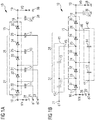
- FIG. 1A shows an exemplary embodiment of a voltage converter 10 that comprises a first, a second and a third capacitor 11 to 13 and a transfer arrangement 15.
- the voltage converter 10 comprises a supply terminal 16 coupled to an input 17 of the transfer arrangement 15.
- the supply terminal 16 may be connected to a not-shown voltage source.
- An output 18 of the transfer arrangement 15 is connected to an output terminal 19 of the voltage converter 10.
- the voltage converter 10 comprises a first and a second clock terminal 21, 22.
- a first electrode of the first capacitor 11 is connected to the first clock terminal 21.
- a second electrode of the first capacitor 11 is connected to a first node 23 of the transfer arrangement 15.
- a first electrode of the second capacitor 12 is connected to the second clock terminal 22.
- a second electrode of the second capacitor 12 is connected to a second node 24 of the transfer arrangement 15.
- a first electrode of the third capacitor 13 is connected to the second electrode of the first capacitor 11.
- a second electrode of the third capacitor 13 is connected to a third node 25 of the transfer arrangement 15.
- the voltage converter 10 may comprise a fourth capacitor 14 having a first electrode that is connected to the second electrode of the second capacitor 12.
- a second electrode of the fourth capacitor 14 may be connected to a fourth node 26 of the transfer arrangement 15.
- the first electrode of the third capacitor 13 is permanently and directly connected to the second electrode of the first capacitor 11.
- the first electrode of the fourth capacitor 14 is permanently and directly connected to the second electrode of the second capacitor 12.
- the first and the second electrode of the third capacitor 13 is free from a direct connection to the first or the second clock terminal 21, 22.
- the first and the second electrode of the fourth capacitor 14 is free from a direct connection to the first or the second clock terminal 21, 22.
- the transfer arrangement 15 comprises a first, a second and a third circuit element 31 to 33.
- the first circuit element 31 couples the input 17 of the transfer arrangement 15 to the first node 23.
- the second circuit element 32 couples the first node 23 to the second node 24.
- the third circuit element 33 couples the second node 24 to the third node 25.
- a fourth circuit element 34 couples the third node 25 to the fourth node 26.
- a final circuit element 35 couples the last node of the transfer arrangement 15 to the output 18 of the transfer arrangement 15. Since, in the embodiment shown in Figure 1A , the last node is the fourth node 26, the final circuit element 35 couples the fourth node 26 to the output 18 of the transfer arrangement 15.
- the transfer arrangement 15 is realized as a series circuit of circuit elements 31 to 34 and the final circuit element 35.
- the transfer arrangement 15 is realized as a series circuit of the first to the fourth circuit element 31 to 34 and the final circuit element 35.
- Each of the circuit elements 31 to 34 and the final circuit element 35 are realized as a diode.
- the transfer arrangement 15 is implemented as a series circuit of diodes. The diodes are oriented in such a way that a current flow is possible from the input 17 of the transfer arrangement 15 to the output 18 of the transfer arrangement 15.
- Each of the diodes may be implemented as a pn-junction. At each of the diodes, the anode is directed to the input 17 and the cathode is oriented to the output 18 of the transfer arrangement 15.
- the voltage converter 10 comprises an output capacitor 37 that couples the output terminal 19 of the voltage converter 10 to a reference potential terminal 38.
- the voltage converter 10 comprises a first and a second stage 27, 28.
- the first stage 27 comprises the first and the second capacitor 11, 12 and the first and the second circuit element 31, 32.
- the second stage 28 comprises the third and the fourth capacitor 13, 14 and the third and the fourth circuit element 33, 34.
- the first and the second capacitor 11, 12 may both have a first capacitance value C1.
- the third and the fourth capacitor 13, 14 may both have a second capacitance value C2.
- the first capacitance value C1 may be larger than the second capacitance value C2, thus C2 ⁇ C1.
- a relationship between C1 and C2 may be: 1.6 • C 2 ⁇ C 1 ⁇ 2.4 • C 2
- the voltage converter 10 comprises further capacitors and circuit elements.
- FIG. 1B shows a further exemplary embodiment of the voltage converter 10.
- the circuit parts and the couplings between the circuit parts of the voltage converter 10 shown in Figure 1B are identical to the circuit parts and couplings of the voltage converter shown in Figure 1A .
- the voltage converter 10 comprises a first series circuit of capacitors 41 and a second series circuit of capacitors 42.
- the first series circuit of capacitors 41 comprises the first and the third capacitor 11, 13.
- the first clock terminal 21 is connected to an outer terminal 43 of the first series circuit of capacitors 41.
- a further outer terminal 45 and nodes between the capacitors 11, 13 of the first series circuit of capacitors 41 are connected to nodes of the transfer arrangement 15.
- the first series circuit of capacitors 41 is connected to the first and the third node 23, 25.
- the second series circuit of capacitors 42 comprises the second and the fourth capacitor 12, 14.
- the second clock terminal 22 is connected to an outer terminal 44 of the second series circuit of capacitors 42.
- Nodes between the capacitors 12, 14 of the second series circuits of capacitors 42 and a further outer terminal 46 of the second series circuit of capacitors 42 are connected to nodes of the transfer arrangement 15. More specifically, the second series circuit of capacitors 42 is connected to the second and the fourth node 24, 26.
- the first series circuit of capacitors 41 comprises the fifth capacitor.
- the second series circuit of capacitors 42 may comprise a sixth capacitor.
- the first series circuit of capacitors 41 has a first number N1 of capacitors.
- the second series circuit of capacitors 42 has a second number N2 of capacitors.
- the first series of capacitors 41 is free from a resistor, diode or transistor connecting one capacitor to the other capacitor of the first series of capacitors 41.
- the connections between the different capacitors of the first series circuit of capacitors 41 only consist of connecting lines.
- the second series of capacitors 42 is free from a resistor, diode or transistor connecting one capacitor to the other capacitor of the second series of capacitors 42.
- the connections between the different capacitors of the second series circuit of capacitors 42 only consist of connecting lines.
- An input voltage VIN is supplied to the supply terminal 16.
- an output voltage VO is provided at the output terminal 19 of the voltage converter 10.
- a first clock signal ⁇ 1 is applied to the first clock terminal 21 and a second clock signal ⁇ 2 is applied to the second clock terminal 22.
- the height of the pulses of the first and the second clock signal ⁇ 1, ⁇ 2 may be equal to the input voltage VIN.
- FIG. 1C shows an exemplary embodiment of the first and the second clock signal ⁇ 1, ⁇ 2 as a function of a time t.
- the voltage converter 10 has a pre-charging mode PM and a charging mode CM.
- the pre-charging mode PM could be called pre-charging phase.
- the charging mode CM could be named charging phase.
- the charging mode CM follows the pre-charging mode PM.
- the input voltage VIN is provided to the voltage converter 10 via the supply terminal 16 and charges the first capacitor 11.
- the pulses of the first clock signal ⁇ 1 and of the second clock signal ⁇ 2 alternate.
- a pulse of the second clock signal ⁇ 2 is between two pulses of the first clock signal ⁇ 1.
- a pulse of the first clock signal ⁇ 1 is between two pulses of the second clock signal ⁇ 2 (with the exception of the first pulse of the first clock signal ⁇ 1).
- a pulse of the first clock signal ⁇ 1 has a first duration T1 and a pulse of the second clock ⁇ 2 signal has a second duration T2.
- the first duration T1 and the second duration T2 may be equal.
- a non-overlap time TN1 between a pulse of the first clock signal ⁇ 1 and the following pulse of the second clock signal ⁇ 2.
- a further non-overlap time TN2 between a pulse of the second clock signal ⁇ 2 and the following pulse of the first clock signal ⁇ 1.
- the non-overlap time TN1 and the further non-overlap time TN2 may have the same duration.
- the period T is repeated periodically.
- the voltage converter 10 operates using four phases.
- a pulse of the first clock signal ⁇ 1 forms a first phase.
- the non-overlap time TN1 realizes a second phase.
- a pulse of the second clock signal ⁇ 2 forms a third phase.
- the further non-overlap time TN2 realizes a fourth phase.
- the efficiency of the voltage converter 10 is increased by the non-overlap times TN1, TN2.
- the input voltage VIN is provided via the first circuit element 31 to the second electrode of the first capacitor 11.
- the input voltage VIN is provided between the two electrodes of the first capacitor 11.
- the charging mode CM by a pulse of the first clock signal ⁇ 1, the input voltage VIN is provided to the first electrode of the first capacitor 11 and thus a voltage tapped at the second electrode of the first capacitor 11 rises to 2 • VIN.
- the input voltage VIN is provided to the first electrode of the second capacitor 12 and thus a voltage tapped at the second electrode of the second capacitor 12 rises up to nearly three times of the input voltage VIN.
- charge flows from the second electrode of the second capacitor 12 via the third circuit element 33 to the second electrode of the third capacitor 13.
- pulses of the first clock signal ⁇ 1 charge stored by the first and the third capacitor 11, 13 is provided via the transfer arrangement 15 to the second and the fourth capacitor 12, 14.
- pulses of the second clock signal ⁇ 2 charge stored by the second and the fourth capacitor 12, 14 is provided via the transfer arrangement 15 to the third capacitor 13 and to the output capacitor 37.
- the second electrode of the first and the second capacitor 11, 12 and both electrodes of the third and the fourth capacitor 13, 14 are charged to the input voltage VIN minus a voltage drop caused by the forward voltage drop VD of the diodes.
- a voltage balancing of the high voltage capacitors 13, 14 is provided by predecessor Dickson stages or stage.
- the predecessor Dickson stage comprises the first and the second capacitor 11, 12. All capacitors see the same forward voltage.
- the capacitors 13, 14 on the right side have the same capacitance value as in the standard Dickson charge pump shown in Figure 4A without stacked capacitors.
- the voltage converter 10 using diodes may be suitable for example at higher values of the input voltage VIN or the output voltage VO. At higher voltages, losses caused by the forward voltage drop VD of the diodes may only have a small effect.
- Figure 2 shows an exemplary embodiment of the voltage converter 10 which is a further development of the voltage converter explained by Figures 1A to 1C .
- the first to the fourth circuit elements 31 to 34 and the final circuit element 35 are realized as transistors.
- the transistors may be implemented as field-effect transistors.
- the transistors of the first to the fourth circuit element 31 to 34 and of the final circuit element 35 are realized as n-channel field-effect transistors.
- the transistors of the first and the third circuit element 31, 33 are controlled by the second clock signal ⁇ 2 and the transistors of the second and the fourth circuit element 32, 34 are controlled by the first clock signal ⁇ 1.
- the final circuit element 35 is controlled by the same signal that is used for the control of the second-last circuit element, namely in the case of Figure 2 by the control signal of the third circuit element 33 that is the second clock signal ⁇ 2. Two consecutive elements of the circuit elements 31 to 34, 35 are not controlled by the same clock signal ⁇ 1, ⁇ 2 and, thus, do not conduct at the same point of time.
- the first to the fourth circuit element 31 to 34 and the final circuit element 35 may be set in a conducting state such that the output voltage VO rises up to the value of the input voltage VIN. Also the first electrodes of the first and the second capacitor 11, 12 are charged such that the input voltage VIN can be tapped between the two electrodes of the first capacitor 11 and between the two electrodes of the second capacitor 12. Additionally, the first and the second electrodes of third and the fourth capacitor 13, 14 are charged to the input voltage VIN in the pre-charging mode PP.
- a higher output voltage VO can be generated by the voltage converter 10 using transistors instead of diodes.
- the maximum of a voltage that is tapped between two electrodes of one of the capacitors 11 to 14 is twice the input voltage VIN.
- each of the capacitors 11 to 14 has to withstand only 2 • VIN. Only the output capacitor 37 has to be fabricated such that it is suitable for operation at higher voltages.
- the transistors may be implemented as p-channel field-effect transistors.
- the first and the third circuit element 31, 33 may be controlled by the inverse signal of the second clock signal ⁇ 2.
- the second and the fourth circuit element 32, 34 may be controlled by the inverse of the first clock signal ⁇ 1.
- the final circuit element 35 may be controlled by the same signal that is used for the control of the second-last circuit element, namely in the case of Figure 2 by the control signal of the third circuit element 33 that is the inverse of the second clock signal ⁇ 2.
- FIG 3A shows a further exemplary embodiment of the voltage converter 10 which is a further development of the embodiments shown in Figures 1A to 1C and 2 .
- the voltage converter 10 comprises the number L of stages.
- the number L is at least 2.
- the first number N1 is equal to the second number N2 and is equal to the number L of stages.
- the voltage converter 10 comprises the first, the second, a third and a fourth stage 27, 28, 48, 49.
- the voltage converter 10 comprises a fifth to an eighth capacitor 50 to 53.
- the third stage 48 comprises the fifth and the sixth capacitor 50, 51.
- the fourth stage 49 comprises the seventh and the eighth capacitor 52, 53.
- a first electrode of the fifth capacitor 50 is permanently and directly connected to the second electrode of the third capacitor 13.
- a second electrode of the fifth capacitor 50 is connected to a fifth node 54 of the transfer arrangement 15.
- a first electrode of the sixth capacitor 51 is directly and permanently connected to the second electrode of the fourth capacitor 14.
- a second electrode of the sixth capacitor 51 is connected to a sixth node 55 of the transfer arrangement 15.
- a first electrode of the seventh capacitor 52 is directly and permanently connected to the second electrode of the fifth capacitor 50.
- a second electrode of the seventh capacitor 52 is connected to a seventh node 56 of the transfer arrangement 15.
- a first electrode of the eighth capacitor 53 is directly and permanently connected to the second electrode of the sixth capacitor 51.
- a second electrode of the eighth capacitor 53 is connected to an eighth node 57 of the transfer arrangement 15.
- the transfer arrangement 15 comprises the number L of switching arrangements 60 to 63 that may be identically realized.
- each of the number L of stages comprises a switching arrangement and two capacitors.
- the first switching arrangement 60 couples the input 17 of the transfer arrangement 15 to a first intermediate node 68 of the transfer arrangement 15.
- the first switching arrangement 60 comprises a first to a fourth switch 64 to 67.
- the first switch 64 couples the input 17 of the transfer arrangement 15 to the first node 23.
- the second switch 65 couples the first node 23 to the first intermediate node 68.
- the third switch 66 couples the second node 24 to the first intermediate node 68.
- the fourth switch 67 couples the input 17 to the second node 24.
- the second switching arrangement 61 couples the first intermediate node 68 to a second intermediate node 73.
- the second switching arrangement 61 is configured such as the first switching arrangement 60.
- the second switching arrangement 61 comprises a fifth to an eighth switch 69 to 72.
- the fifth switch 69 couples the first intermediate node 68 to the third node 25.
- the sixth switch 70 couples the third node 25 to the second intermediate node 73.
- the seventh switch 71 couples the fourth node 26 to the second intermediate node 73.
- the eighth switch 72 couples the first intermediate node 68 to the fourth node 26.
- the third switching arrangement 62 couples the second intermediate node 73 to a third intermediate node 78.
- the third switching arrangement 62 comprises a ninth to a twelfth switch 74 to 77.
- the fourth switching arrangement 63 comprises a thirteenth to a sixteenth switch 79 to 82.
- the fourth switching arrangement 63 couples the third intermediate node 78 to the output 18 of the transfer arrangement 15.
- the third and the fourth switching arrangement 62, 63 are realized such as the first and the second switching arrangement 60, 61.
- the switches of the transfer arrangement 15 are realized as field-effect transistors.
- the switches of the transfer arrangement 15 may be realized as n-channel field-effect transistors.
- the fifth and the sixth capacitor 50, 51 may both have a third capacitance value C3.
- the seventh and the eighth capacitor 52, 53 may both have a fourth capacitance value C4.
- a relationship between C1, C2, C3 and C4 may be: C 4 ⁇ C 3 ⁇ C 2 ⁇ C 1 , wherein C1 is the capacitance value of the two capacitors 11, 12 of the first stage 27, C2 is the capacitance value of the two capacitors 13, 14 of the second stage 28, C3 is the capacitance value of the two capacitors 50, 51 of the third stage 48, and C4 is the capacitance value of the two capacitors 52, 53 of the fourth stage 49.
- the first clock signal ⁇ 1 controls the second switch 65 of the first switching arrangement 60. Furthermore, the first clock signal ⁇ 1 controls the corresponding switches in the further switching arrangements 61 to 63, namely the sixth switch 70 of the second switching arrangement 61, the tenth switch 75 of the third switching arrangement 62 and the fourteenth switch 80 of the fourth switching arrangement 63.
- the second control signal ⁇ 2 controls the first switch 64 of the first switching arrangement 60.
- the second clock signal ⁇ 2 controls the corresponding switches in the further switching arrangements 61 to 63, namely the fifth switch 69 of the second switching arrangement 61, the ninth switch 74 of the third switching arrangement 62 and the thirteenth switch 79 of the fourth switching arrangement 63.
- a third control signal ⁇ 3 controls the third switch 66 of the first switching arrangement 60.
- the third clock signal ⁇ 3 controls the corresponding switches in the further switching arrangements 61 to 63, namely the seventh switch 71 of the second switching arrangement 61, the eleventh switch 76 of the third switching arrangement 62 and the fifteenth switch 81 of the fourth switching arrangement 63.
- a fourth control signal ⁇ 4 controls the fourth switch 67 of the first switching arrangement 60.
- the fourth clock signal ⁇ 4 controls the corresponding switches in the further switching arrangements 61 to 63, namely the eight switch 72 of the second switching arrangement 61, the twelfth switch 77 of the third switching arrangement 62 and the sixteenth switch 82 of the fourth switching arrangement 63.
- the first clock signal ⁇ 1 sets the switches that are controlled by the first clock signal ⁇ 1 in a conducting state during a pulse.
- the second to the fourth clock signal ⁇ 2, ⁇ 3, ⁇ 4 set the switches that are controlled by these clock signals in a conducting state during a pulse of these clock signals.
- the first and the fourth switch 64, 67 may be set in a conducting state.
- the first and the second capacitor 11, 12 are charged by the input voltage VIN during the pre-charging mode PP.
- the first and the second clock signal ⁇ 1, ⁇ 2 are generated such as shown in Figure 1C .
- the third clock signal ⁇ 3 may have the pulses of the first clock signal ⁇ 1 and of the second clock signal ⁇ 2 in the charging mode CP.
- the fourth clock signal ⁇ 4 constantly has the value 0.
- the switches controlled by the fourth clock signal ⁇ 4 are permanently in a non-conducting state in the charging mode CP.
- the voltage converter 10 is realized as a four-stage Dickson charge pump with modified topology.
- each of the switches 64 to 67, 69 to 72, 74 to 77, 79 to 82 of the four switching arrangements 60 to 63 are set in a conducting state.
- the output voltage VO has the value of the input voltage VIN.
- the third clock signal ⁇ 3 constantly has the value 1.
- the switches controlled by the third clock signal ⁇ 3 are permanently in a conducting state in the charging mode CP.
- the third switch 66, the seventh switch 71, the eleventh switch 76 and the fifteenth switch 81 are replaced by conducting lines.
- the fourth switch 67, the eight switch 72, the twelfth switch 77 and the sixteenth switch 82 can be omitted.
- the fourth stage 49 is omitted.
- the third intermediate node 78 is directly connected to the output 18 of the transfer arrangement 15.
- the third and the fourth stage 48, 49 is omitted.
- the second intermediate node 73 is directly connected to the output 18 of the transfer arrangement 15.
- the switches of the transfer arrangement 15 may be realized as p-channel field-effect transistors.
- the clock signals ⁇ 1 to ⁇ 4 may be replaced by the corresponding inverse clock signals, as explained regarding Figure 2 .
- the voltage converter 10 comprises further stages that couple the fourth stage 49 to the output 18.
- FIG. 3B shows a further exemplary embodiment of the voltage converter 10 that is a further development of the above-shown embodiments.
- the voltage converter 10 comprises a first backup capacitor 85 coupling the first intermediate node 68 to the reference potential terminal 38.
- the voltage converter 10 comprises a second backup capacitor 86 coupling the second intermediate node 73 to the first intermediate node 68.
- the voltage converter 10 comprises a third backup capacitor 87 coupling the output 18 of the transfer arrangement 15 to the second intermediate node 73.
- the output terminal 19 of the voltage converter 10 is coupled via a series circuit of backup capacitors 85 to 87 to the reference potential terminal 38.
- the voltage converter 10 comprises the number L of stages.
- the number of back-up capacitors 85 to 87 is equal to the number L of stages 27, 28, 48.
- the voltage converter 10 comprises the number L of backup capacitors 85 to 87 which are arranged in a series circuit between the output terminal 19 and the reference potential terminal 38.
- the voltage converter 10 comprises 2 • L capacitors 11 to 14,50,51.
- the number L is three (the first number N1 and the second number N2 equals 3).
- the voltage converter 10 comprises exactly three stages 27, 28, 48. Consequently, the transfer arrangement 15 comprises exactly three back-up capacitors 85 to 87, three switching arrangements 61 to 63 and 2 ⁇ 3 capacitors, namely six capacitors 11 to 14, 50, 51.
- the output voltage VO does not drop across any of the capacitors 11 to 14, 50 to 53, 85 to 87.
- Each of these capacitors only has to withstand a portion of the output voltage VO.
- stress on the capacitors is reduced.
- a single output capacitor such as the output capacitor 37 shown in Figures 1A, 1B and 2 can be added to the voltage converter 10 shown in Figures 3A and 3B , but can be left out using the three backup capacitors 85 to 87.
- FIGS 4A show an exemplary embodiment of the voltage converter 10 for illustrative purposes.
- the voltage converter 10 is implemented as a standard Dickson charge pump.
- the first electrode of the third capacitor 13 is connected to the first clock terminal 21 and is not connected to the second electrode of the second capacitor 12.
- the first electrode of the fourth capacitor 14 is connected to the second clock terminal 22 and is not connected to the second electrode of the third capacitor 13.
- the third and the fourth capacitors 13, 14 are realized as high voltage capacitors.
- FIGS. 4B show an exemplary embodiment of the voltage converter 10 for illustrative purposes.
- a series circuit of the third capacitor 13 and a further third capacitor 100 couples the first clock terminal 21 to the third node 25.
- a series circuit of the fourth capacitor 14 and a further fourth capacitor 101 couples the second clock terminal 22 to the fourth node 26.
- a first resistor 102 is connected in parallel to the third capacitor 13.
- a second resistor 103 is connected in parallel to the further third capacitor 100.
- a third resistor 104 is connected in parallel to the fourth capacitor 14.
- a fourth resistor 105 is connected in parallel to the further fourth capacitor 105.
- a voltage across the third capacitor 13 is nearly equal to a voltage across the further third capacitor 100 due to the first and the second resistor 102, 103.
- the voltage converter 10 is implemented as a modified Dickson charge pump with low-voltage capacitors 11 to 14, 100, 101 and balancing resistors 102 to 105.
- Figure 4C shows an exemplary embodiment of signals of different voltage converters. The signals were generated by simulation.
- the output voltage VO is shown as a function of the time t.
- an input current IN flowing to the voltage converter 10 via the supply terminal 16 and the first and the second clock terminal 21, 22 is shown as a function of the time t.
- the curve A show the output voltage VO and the input current IN of the voltage converter 10 illustrated by Figure 3A having four stages.
- Curve B shows the output voltage VO and the input current IN of a Dickson charge pump comprising high voltage capacitors as explained in Figure 4A .
- Curve C shows the output voltage VO and the input current IN of a voltage converter implemented as a Dickson charge pump wherein the high voltage capacitors are replaced by stacked capacitors as illustrated in Figure 4B .
- t 2.6 microsecond
- no load current flows through the output terminal 19 of the voltage converter 10.
- the output voltage VO is rising whereas the input current IN drops as a function of the time t.
- the voltage converter 10 with four stages has a charge pump efficiency of 35.1 %, an input current IN of 0.87 mA, an output voltage VO of 9.07 V and uses a capacitor array of 60 pF.
- the standard Dickson charge pump of Figure 4A with high-voltage capacitors achieves a charge pump efficiency of 45.3 %, an input current IN of 0.81 mA, an output voltage VO of 10.96 V and uses a capacitor array of 16 pF.
- the Dickson charge pump with low-voltage capacitors and balancing resistors of Figure 4B achieves a charge pump efficiency of 18.9 %, an input current IN of 1.59 mA, an output voltage VO of 9.05 V and uses a capacitor array of 120 pF as well as a resistor array of 18 MOhm.
- the voltage converters 10 of Figures 1A to 1C, 2, 3A and 3B are configured as arrangements of flying capacitors without need of balancing resistors.
- a power consumption and area of balancing resistors is eliminated by the voltage converters 10 of Figures 1A to 1C, 2, 3A and 3B .
- the capacitors 50 to 53 on the right side have the same capacitance value as in the non-stacked version with high-voltage capacitors.
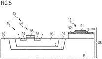
- FIG. 5 shows an exemplary embodiment of a semiconductor body 88 comprising the voltage converter 10.
- a cross section of the semiconductor body 88 is shown.
- the semiconductor body 88 comprises the transfer arrangement 15 and the capacitors 11 to 14.
- the first switch 64 and the first capacitor 11 is illustrated.
- the semiconductor body 88 comprises a semiconductor substrate 89.
- the capacitors 11 to 14 are fabricated as metal-isolator-metal capacitors.
- the first electrode of the first capacitor 11 is realized as a first conducting layer 90 and the second electrode of the first capacitor 11 is realized as a second conducting layer 91.
- the first and the second conducting layer 90, 91 may be realized as metal and/or polysilicon and/or silicide layers.
- An isolating layer 92 is arranged between the first and the second conducting layer 90, 91.
- the first capacitor 11 is separated from the semiconductor substrate 89 by at least a further isolating layer 93.
- the not-shown output capacitor 37 may be realized as a metal-isolator-metal capacitor, metal or polysilicon to substrate capacitor or as an external capacitor outside of the semiconductor body 88.
- the first switch 64 is realized as field-effect transistor.
- the first switch 64 comprises a source region 94, a drain region 95, a gate 98 and a channel.
- the source region 94, the drain region 95 and the channel are arranged in a well 96.
- the well is located in a deep well 97.
- the deep well 97 is arranged in the semiconductor substrate 89.
- the first switch 64 is realized as n-channel field-effect transistor.
- the source region 94 and the drain region 95 are n-doped.
- the well 96 is fabricated as a p-well.
- the deep well 97 is realized as a deep n-well.
- the semiconductor substrate 89 is p-doped.
- the first switch 64 is realized as p-channel field-effect transistor.
- the field-effect transistor of the first circuit element 31, shown in Figure 2 may also be realized as the field-effect transistor illustrated in Figure 5 .
- the transfer arrangement 15 and the first to the fourth capacitor 11 to 14 are integrated in the semiconductor body 88. This is a result of the reduction of the voltage across the capacitors 11 to 14.
Landscapes
- Engineering & Computer Science (AREA)
- Power Engineering (AREA)
- Dc-Dc Converters (AREA)
Abstract
Description
- The present patent application is related to a voltage converter and a method for voltage conversion.
- Voltage converters often convert a DC voltage into another DC voltage. A voltage converter can be realized as a charge pump comprising several capacitors that are charged and discharged during operation. The capacitors may have a maximum operating voltage.
- It is an object of the present patent application to provide a voltage converter and a method for voltage conversion with a reduced voltage across capacitors of the voltage converter.
- This object is solved by the independent claims. Further developments and embodiments are described in the dependent claims.
- In an embodiment, a voltage converter comprises a first, a second and a third capacitor, a first and a second clock terminal, a supply terminal and a transfer arrangement. An input of the transfer arrangement is coupled to the supply terminal and an output of the transfer arrangement is coupled to an output terminal of the voltage converter. A first electrode of the first capacitor is connected to the first clock terminal and a second electrode of the first capacitor is connected to a first node of the transfer arrangement. A first electrode of the second capacitor is connected to the second clock terminal and a second electrode of the second capacitor is connected to a second node of the transfer arrangement. A first electrode of the third capacitor is permanently and directly connected to the second electrode of the first capacitor and a second electrode of the third capacitor is connected to a third node of the transfer arrangement.
- Advantageously, the first and the second clock terminal are not directly connected to the third capacitor. Thus, during operation a reference potential is not provided to the first or the second electrode of the third capacitor. The voltage difference between the two electrodes of the third capacitor is equal or less than the twofold of an input voltage tapped at the supply terminal.
- In an embodiment, the voltage converter comprises a fourth capacitor having a first electrode permanently and directly connected to the second electrode of the second capacitor and a second electrode connected to a fourth node of the transfer arrangement.
- In an embodiment, the voltage converter comprises at least a Nth capacitor having a first electrode permanently and directly connected to the second electrode of the (N-2)th capacitor and a second electrode connected to a Nth node of the transfer arrangement, wherein N is larger than 4. N may be 5, 6 and so on. Thus, a first electrode of the fifth capacitor is permanently and directly connected to the second electrode of the third capacitor. A first electrode of the sixth capacitor is permanently and directly connected to the second electrode of the fourth capacitor and so forth.
- In an embodiment, the transfer arrangement comprises a first, a second and a third circuit element. The first circuit element couples the supply terminal to the first node, the second circuit element couples the first node to the second node and the third circuit element couples the second node to the third node.
- In an embodiment, the third node is coupled to the output of the transfer arrangement by a final circuit element or by a series circuit of the final circuit element and at least a further circuit element.
- In an embodiment, each of the first, the second and the third circuit element is realized as a diode. The final circuit element and/or further circuit elements may also be realized as a diode.
- In an alternative embodiment, each of the first, the second and the third circuit element is realized as a field-effect transistor. The final circuit element and/or further circuit elements may also be realized as a field-effect transistor.
- In an embodiment, the voltage converter comprises an output capacitor coupling the output of the transfer arrangement to a reference potential terminal.
- In an alternative embodiment, the voltage converter is free from any capacitor having a first electrode directly connected to the output of the transfer arrangement and a second electrode directly connected to the reference potential terminal.
- In an embodiment, the voltage converter comprises a first switching arrangement having a first and a second switch. The first switch couples the input of the transfer arrangement to the first node. The second switch couples the first node to a first intermediate node of the transfer arrangement.
- In a further development, the first switching arrangement comprises a third switch that couples the second node to the first intermediate node of the transfer arrangement.
- The first switching arrangement may optionally comprise a fourth switch that couples the input of the transfer arrangement to the second node.
- In an embodiment, the voltage converter comprises a first back-up capacitor coupling the first intermediate node to the reference potential terminal.
- In an embodiment, the voltage converter comprises a second switching arrangement having a fifth and a sixth switch. The fifth switch couples the first intermediate node to the third node. The sixth switch couples the third node to a second intermediate node of the transfer arrangement.
- The second switching arrangement may optionally comprise a seventh switch that couples the fourth node to the second intermediate node of the transfer arrangement.
- The second switching arrangement may optionally comprise an eighth switch coupling the first intermediate node to the fourth node.
- In an embodiment, the voltage converter comprises a second back-up capacitor coupling the second intermediate node to the first intermediate node.
- In an embodiment, the voltage converter is realized as a Dickson charge pump capacitor arrangement. The voltage converter is configured for generating a higher output voltage at the output terminal. The voltage converter is designed as an internal charge pump for an output voltage above the maximum operating voltage of the capacitors used. The voltage converter provides an improved charge pump efficiency and a reduced size.
- In an embodiment, a method for voltage conversion comprises providing an input voltage to an input of a transfer arrangement, providing a first clock signal to a first electrode of a first capacitor, providing a second clock signal to a first electrode of a second capacitor and tapping an output voltage at an output of the transfer arrangement. A second electrode of the first capacitor is connected to a first node of the transfer arrangement. A second electrode of the second capacitor is connected to a second node of the transfer arrangement. A first electrode of a third capacitor is permanently and directly connected to the second electrode of the first capacitor. A second electrode of the third capacitor is connected to a third node of the transfer arrangement.
- Advantageously, the first and the second clock signal are not directly applied to the third capacitor. Thus, during operation a reference potential is not provided to the first or the second electrode of the third capacitor. The voltage difference between the two electrodes of the third capacitor is equal or less than twice of the input voltage. Thus, the voltage across the third capacitor is reduced.
- In an embodiment, pulses of the first clock signal and pulses of the second clock signal alternate. One pulse of the second clock signal is between two pulses of the first clock signal and so forth.
- In an embodiment, a method for voltage conversion comprises providing an input voltage to an input of the transfer arrangement, providing a first clock signal to an outer terminal of a first series circuit of capacitors, providing a second clock signal to an outer terminal of a second series circuit of capacitors and tapping an output voltage at an output of the transfer arrangement.
- In an embodiment, the first series of capacitors comprises a first and a third capacitor. The second series of capacitors comprises a second and a fourth capacitor.
- In an embodiment, a further outer terminal of the first series circuit of capacitors and a node or nodes between capacitors of the first series circuit of capacitors and a further outer terminal of the second series circuit of capacitors and a node or nodes between capacitors of the second series circuit of capacitors are connected to different nodes of the transfer arrangement. Thus, charges are provided from the first series of capacitors to the second series of capacitors via the transfer arrangement at a pulse of the first clock signal and charges are provided from the second series of capacitors to the first series of capacitors via the transfer arrangement at a pulse of the second clock signal.
- The following description of figures of exemplary embodiments may further illustrate and explain aspects of the invention. Devices and circuit parts with the same structure and the same effect, respectively, appear with equivalent reference symbols. In so far as devices or circuit parts correspond to one another in terms of their function in different figures, the description thereof is not repeated for each of the following figures.
- Figures 1A to 1C
- show exemplary embodiments of a voltage converter.
- Figure 2
- shows a further exemplary embodiment of a voltage converter.
- Figures 3A and 3B
- show further exemplary embodiments of a voltage converter.
- Figures 4A to 4C
- show exemplary embodiments of voltage converters and of signals that can be tapped at voltage converters.
- Figure 5
- shows an exemplary embodiment of a semiconductor body comprising a voltage converter.
-
Figure 1A shows an exemplary embodiment of avoltage converter 10 that comprises a first, a second and athird capacitor 11 to 13 and atransfer arrangement 15. Thevoltage converter 10 comprises asupply terminal 16 coupled to aninput 17 of thetransfer arrangement 15. Thesupply terminal 16 may be connected to a not-shown voltage source. Anoutput 18 of thetransfer arrangement 15 is connected to anoutput terminal 19 of thevoltage converter 10. Moreover, thevoltage converter 10 comprises a first and asecond clock terminal first capacitor 11 is connected to thefirst clock terminal 21. A second electrode of thefirst capacitor 11 is connected to afirst node 23 of thetransfer arrangement 15. A first electrode of thesecond capacitor 12 is connected to thesecond clock terminal 22. A second electrode of thesecond capacitor 12 is connected to asecond node 24 of thetransfer arrangement 15. A first electrode of thethird capacitor 13 is connected to the second electrode of thefirst capacitor 11. Furthermore, a second electrode of thethird capacitor 13 is connected to athird node 25 of thetransfer arrangement 15. - Moreover, the
voltage converter 10 may comprise afourth capacitor 14 having a first electrode that is connected to the second electrode of thesecond capacitor 12. A second electrode of thefourth capacitor 14 may be connected to afourth node 26 of thetransfer arrangement 15. - The first electrode of the
third capacitor 13 is permanently and directly connected to the second electrode of thefirst capacitor 11. Correspondingly, the first electrode of thefourth capacitor 14 is permanently and directly connected to the second electrode of thesecond capacitor 12. The first and the second electrode of thethird capacitor 13 is free from a direct connection to the first or thesecond clock terminal fourth capacitor 14 is free from a direct connection to the first or thesecond clock terminal - The
transfer arrangement 15 comprises a first, a second and athird circuit element 31 to 33. Thefirst circuit element 31 couples theinput 17 of thetransfer arrangement 15 to thefirst node 23. Thesecond circuit element 32 couples thefirst node 23 to thesecond node 24. Correspondingly, thethird circuit element 33 couples thesecond node 24 to thethird node 25. Afourth circuit element 34 couples thethird node 25 to thefourth node 26. Afinal circuit element 35 couples the last node of thetransfer arrangement 15 to theoutput 18 of thetransfer arrangement 15. Since, in the embodiment shown inFigure 1A , the last node is thefourth node 26, thefinal circuit element 35 couples thefourth node 26 to theoutput 18 of thetransfer arrangement 15. - Thus, the
transfer arrangement 15 is realized as a series circuit ofcircuit elements 31 to 34 and thefinal circuit element 35. In the example shown inFigure 1A , thetransfer arrangement 15 is realized as a series circuit of the first to thefourth circuit element 31 to 34 and thefinal circuit element 35. Each of thecircuit elements 31 to 34 and thefinal circuit element 35 are realized as a diode. Thetransfer arrangement 15 is implemented as a series circuit of diodes. The diodes are oriented in such a way that a current flow is possible from theinput 17 of thetransfer arrangement 15 to theoutput 18 of thetransfer arrangement 15. Each of the diodes may be implemented as a pn-junction. At each of the diodes, the anode is directed to theinput 17 and the cathode is oriented to theoutput 18 of thetransfer arrangement 15. - The
voltage converter 10 comprises anoutput capacitor 37 that couples theoutput terminal 19 of thevoltage converter 10 to a referencepotential terminal 38. - The
voltage converter 10 comprises a first and asecond stage first stage 27 comprises the first and thesecond capacitor second circuit element second stage 28 comprises the third and thefourth capacitor fourth circuit element - The first and the
second capacitor fourth capacitor 
- For example: C1 = 2 • C2
- In an alternative, not shown embodiment, the
voltage converter 10 comprises further capacitors and circuit elements. -
Figure 1B shows a further exemplary embodiment of thevoltage converter 10. The circuit parts and the couplings between the circuit parts of thevoltage converter 10 shown inFigure 1B are identical to the circuit parts and couplings of the voltage converter shown inFigure 1A . Thevoltage converter 10 comprises a first series circuit ofcapacitors 41 and a second series circuit ofcapacitors 42. The first series circuit ofcapacitors 41 comprises the first and thethird capacitor first clock terminal 21 is connected to anouter terminal 43 of the first series circuit ofcapacitors 41. A furtherouter terminal 45 and nodes between thecapacitors capacitors 41 are connected to nodes of thetransfer arrangement 15. Thus, the first series circuit ofcapacitors 41 is connected to the first and thethird node - Correspondingly, the second series circuit of
capacitors 42 comprises the second and thefourth capacitor second clock terminal 22 is connected to anouter terminal 44 of the second series circuit ofcapacitors 42. Nodes between thecapacitors capacitors 42 and a furtherouter terminal 46 of the second series circuit ofcapacitors 42 are connected to nodes of thetransfer arrangement 15. More specifically, the second series circuit ofcapacitors 42 is connected to the second and thefourth node - In case the
voltage converter 10 has a fifth capacitor, the first series circuit ofcapacitors 41 comprises the fifth capacitor. Additionally, the second series circuit ofcapacitors 42 may comprise a sixth capacitor. - The first series circuit of
capacitors 41 has a first number N1 of capacitors. Correspondingly, the second series circuit ofcapacitors 42 has a second number N2 of capacitors. The first number N1 and the second number N2 follow the subsequent equations:
- The first series of
capacitors 41 is free from a resistor, diode or transistor connecting one capacitor to the other capacitor of the first series ofcapacitors 41. The connections between the different capacitors of the first series circuit ofcapacitors 41 only consist of connecting lines. Correspondingly, the second series ofcapacitors 42 is free from a resistor, diode or transistor connecting one capacitor to the other capacitor of the second series ofcapacitors 42. The connections between the different capacitors of the second series circuit ofcapacitors 42 only consist of connecting lines. - An input voltage VIN is supplied to the
supply terminal 16. At theoutput terminal 19 of thevoltage converter 10 an output voltage VO is provided. A first clock signal Φ1 is applied to thefirst clock terminal 21 and a second clock signal Φ2 is applied to thesecond clock terminal 22. The height of the pulses of the first and the second clock signal Φ1, Φ2 may be equal to the input voltage VIN. -
Figure 1C shows an exemplary embodiment of the first and the second clock signal Φ1, Φ2 as a function of a time t. Thevoltage converter 10 has a pre-charging mode PM and a charging mode CM. The pre-charging mode PM could be called pre-charging phase. The charging mode CM could be named charging phase. The charging mode CM follows the pre-charging mode PM. In the pre-charging mode PM, the input voltage VIN is provided to thevoltage converter 10 via thesupply terminal 16 and charges thefirst capacitor 11. - In the charging mode CM, the pulses of the first clock signal Φ1 and of the second clock signal Φ2 alternate. Thus, a pulse of the second clock signal Φ2 is between two pulses of the first clock signal Φ1. Correspondingly, a pulse of the first clock signal Φ1 is between two pulses of the second clock signal Φ2 (with the exception of the first pulse of the first clock signal Φ1). A pulse of the first clock signal Φ1 has a first duration T1 and a pulse of the second clock Φ2 signal has a second duration T2. The first duration T1 and the second duration T2 may be equal.
- There is a non-overlap time TN1 between a pulse of the first clock signal Φ1 and the following pulse of the second clock signal Φ2. There is also a further non-overlap time TN2 between a pulse of the second clock signal Φ2 and the following pulse of the first clock signal Φ1. The non-overlap time TN1 and the further non-overlap time TN2 may have the same duration. Thus, a period T of the clock signals Φ1, Φ2 can be calculated according to the following equation:

- Thus, the period T is repeated periodically. In the charging mode CM, the
voltage converter 10 operates using four phases. A pulse of the first clock signal Φ1 forms a first phase. The non-overlap time TN1 realizes a second phase. A pulse of the second clock signal Φ2 forms a third phase. The further non-overlap time TN2 realizes a fourth phase. Advantageously, the efficiency of thevoltage converter 10 is increased by the non-overlap times TN1, TN2. - At the start of operation, in the pre-charging mode PM, the input voltage VIN is provided via the
first circuit element 31 to the second electrode of thefirst capacitor 11. Thus, the input voltage VIN is provided between the two electrodes of thefirst capacitor 11. In the charging mode CM, by a pulse of the first clock signal Φ1, the input voltage VIN is provided to the first electrode of thefirst capacitor 11 and thus a voltage tapped at the second electrode of thefirst capacitor 11 rises to 2 • VIN. Thus, charge flows from the second electrode of thefirst capacitor 11 via thesecond circuit element 32 to the second electrode of thesecond capacitor 12. - By a pulse of the second clock signal Φ2, the input voltage VIN is provided to the first electrode of the
second capacitor 12 and thus a voltage tapped at the second electrode of thesecond capacitor 12 rises up to nearly three times of the input voltage VIN. Thus, charge flows from the second electrode of thesecond capacitor 12 via thethird circuit element 33 to the second electrode of thethird capacitor 13. - By the following pulses of the first clock signal Φ1, charge stored by the first and the
third capacitor transfer arrangement 15 to the second and thefourth capacitor fourth capacitor transfer arrangement 15 to thethird capacitor 13 and to theoutput capacitor 37. - In the pre-charging mode PM, the second electrode of the first and the
second capacitor fourth capacitor output capacitor 37 may be charged up to the following value:

capacitors 11 to 14 of the first and the second series circuit ofcapacitors capacitors 11 to 14 coupled to thetransfer arrangement 15 besides theoutput capacitor 37. Thus, the number of diodes is N + 1. An output current flowing from thevoltage converter 10 to a not-shown load is neglected in the equations above. - Advantageously, a voltage balancing of the
high voltage capacitors second capacitor capacitors Figure 4A without stacked capacitors. Just thecapacitors right capacitors Figure 4B that may increase the size of thevoltage converter 10 and reduce efficiency. - Advantageously, the
voltage converter 10 using diodes may be suitable for example at higher values of the input voltage VIN or the output voltage VO. At higher voltages, losses caused by the forward voltage drop VD of the diodes may only have a small effect.Figure 2 shows an exemplary embodiment of thevoltage converter 10 which is a further development of the voltage converter explained byFigures 1A to 1C . The first to thefourth circuit elements 31 to 34 and thefinal circuit element 35 are realized as transistors. The transistors may be implemented as field-effect transistors. For example, the transistors of the first to thefourth circuit element 31 to 34 and of thefinal circuit element 35 are realized as n-channel field-effect transistors. In this case, the transistors of the first and thethird circuit element fourth circuit element final circuit element 35 is controlled by the same signal that is used for the control of the second-last circuit element, namely in the case ofFigure 2 by the control signal of thethird circuit element 33 that is the second clock signal Φ2. Two consecutive elements of thecircuit elements 31 to 34, 35 are not controlled by the same clock signal Φ1, Φ2 and, thus, do not conduct at the same point of time. - In the
voltage converter 10 shown inFigure 2 , in the pre-charging mode PP, the first to thefourth circuit element 31 to 34 and thefinal circuit element 35 may be set in a conducting state such that the output voltage VO rises up to the value of the input voltage VIN. Also the first electrodes of the first and thesecond capacitor first capacitor 11 and between the two electrodes of thesecond capacitor 12. Additionally, the first and the second electrodes of third and thefourth capacitor - In case there is no load connected to the
output terminal 19 of thevoltage converter 10 and after several pulses of the first and the second clock signal Φ1, Φ2 and by neglecting a voltage drop at the transistors of thetransfer arrangement 15, the output voltage VO may rise to the following value:

capacitors 11 to 14 of the first and thesecond series circuit capacitors 11 to 14 coupled to thetransfer arrangement 15 besides theoutput capacitor 37. - Advantageously, a higher output voltage VO can be generated by the
voltage converter 10 using transistors instead of diodes. Advantageously, the maximum of a voltage that is tapped between two electrodes of one of thecapacitors 11 to 14 is twice the input voltage VIN. Thus, each of thecapacitors 11 to 14 has to withstand only 2 • VIN. Only theoutput capacitor 37 has to be fabricated such that it is suitable for operation at higher voltages. - In an alternative, not-shown embodiment, the transistors may be implemented as p-channel field-effect transistors. The first and the
third circuit element fourth circuit element final circuit element 35 may be controlled by the same signal that is used for the control of the second-last circuit element, namely in the case ofFigure 2 by the control signal of thethird circuit element 33 that is the inverse of the second clock signal Φ2. -
Figure 3A shows a further exemplary embodiment of thevoltage converter 10 which is a further development of the embodiments shown inFigures 1A to 1C and 2 . Thevoltage converter 10 comprises the number L of stages. The number L is at least 2. The first number N1 is equal to the second number N2 and is equal to the number L of stages. In the example shown inFigure 3A , N1 = N2 = L = 4. Thus, thevoltage converter 10 comprises the first, the second, a third and afourth stage voltage converter 10 comprises a fifth to aneighth capacitor 50 to 53. Thethird stage 48 comprises the fifth and thesixth capacitor fourth stage 49 comprises the seventh and theeighth capacitor - A first electrode of the
fifth capacitor 50 is permanently and directly connected to the second electrode of thethird capacitor 13. A second electrode of thefifth capacitor 50 is connected to afifth node 54 of thetransfer arrangement 15. A first electrode of thesixth capacitor 51 is directly and permanently connected to the second electrode of thefourth capacitor 14. A second electrode of thesixth capacitor 51 is connected to asixth node 55 of thetransfer arrangement 15. A first electrode of theseventh capacitor 52 is directly and permanently connected to the second electrode of thefifth capacitor 50. Moreover, a second electrode of theseventh capacitor 52 is connected to aseventh node 56 of thetransfer arrangement 15. A first electrode of theeighth capacitor 53 is directly and permanently connected to the second electrode of thesixth capacitor 51. A second electrode of theeighth capacitor 53 is connected to aneighth node 57 of thetransfer arrangement 15. - The
transfer arrangement 15 comprises the number L of switchingarrangements 60 to 63 that may be identically realized. Thus, each of the number L of stages comprises a switching arrangement and two capacitors. Each of the switchingarrangements 60 to 63 is coupled to one capacitor of the first series circuit ofcapacitors 41 and to one capacitor of the second series circuit ofcapacitors 42. Since in the example shown inFigure 3A N1 = N2 = L = 4, thetransfer arrangement 15 comprises a first to afourth switching arrangement 60 to 63. - The
first switching arrangement 60 couples theinput 17 of thetransfer arrangement 15 to a firstintermediate node 68 of thetransfer arrangement 15. Thefirst switching arrangement 60 comprises a first to afourth switch 64 to 67. Thefirst switch 64 couples theinput 17 of thetransfer arrangement 15 to thefirst node 23. Thesecond switch 65 couples thefirst node 23 to the firstintermediate node 68. Moreover, thethird switch 66 couples thesecond node 24 to the firstintermediate node 68. Thefourth switch 67 couples theinput 17 to thesecond node 24. - The
second switching arrangement 61 couples the firstintermediate node 68 to a secondintermediate node 73. Thesecond switching arrangement 61 is configured such as thefirst switching arrangement 60. Thesecond switching arrangement 61 comprises a fifth to aneighth switch 69 to 72. Thefifth switch 69 couples the firstintermediate node 68 to thethird node 25. Thesixth switch 70 couples thethird node 25 to the secondintermediate node 73. Moreover, theseventh switch 71 couples thefourth node 26 to the secondintermediate node 73. Theeighth switch 72 couples the firstintermediate node 68 to thefourth node 26. - The
third switching arrangement 62 couples the secondintermediate node 73 to a thirdintermediate node 78. Thethird switching arrangement 62 comprises a ninth to atwelfth switch 74 to 77. - Moreover, the
fourth switching arrangement 63 comprises a thirteenth to asixteenth switch 79 to 82. Thefourth switching arrangement 63 couples the thirdintermediate node 78 to theoutput 18 of thetransfer arrangement 15. The third and thefourth switching arrangement second switching arrangement - The switches of the
transfer arrangement 15 are realized as field-effect transistors. The switches of thetransfer arrangement 15 may be realized as n-channel field-effect transistors. - The fifth and the
sixth capacitor eighth capacitor 
capacitors first stage 27, C2 is the capacitance value of the twocapacitors second stage 28, C3 is the capacitance value of the twocapacitors third stage 48, and C4 is the capacitance value of the twocapacitors fourth stage 49. - For example: 8 • C4 = 4 • C3 = 2 • C2 = C1
- The first clock signal Φ1 controls the
second switch 65 of thefirst switching arrangement 60. Furthermore, the first clock signal Φ1 controls the corresponding switches in thefurther switching arrangements 61 to 63, namely thesixth switch 70 of thesecond switching arrangement 61, thetenth switch 75 of thethird switching arrangement 62 and thefourteenth switch 80 of thefourth switching arrangement 63. - The second control signal Φ2 controls the
first switch 64 of thefirst switching arrangement 60. Correspondingly, the second clock signal Φ2 controls the corresponding switches in thefurther switching arrangements 61 to 63, namely thefifth switch 69 of thesecond switching arrangement 61, theninth switch 74 of thethird switching arrangement 62 and thethirteenth switch 79 of thefourth switching arrangement 63. - A third control signal Φ3 controls the
third switch 66 of thefirst switching arrangement 60. Correspondingly, the third clock signal Φ3 controls the corresponding switches in thefurther switching arrangements 61 to 63, namely theseventh switch 71 of thesecond switching arrangement 61, theeleventh switch 76 of thethird switching arrangement 62 and thefifteenth switch 81 of thefourth switching arrangement 63. - A fourth control signal Φ4 controls the
fourth switch 67 of thefirst switching arrangement 60. Correspondingly, the fourth clock signal Φ4 controls the corresponding switches in thefurther switching arrangements 61 to 63, namely the eightswitch 72 of thesecond switching arrangement 61, thetwelfth switch 77 of thethird switching arrangement 62 and thesixteenth switch 82 of thefourth switching arrangement 63. - The first clock signal Φ1 sets the switches that are controlled by the first clock signal Φ1 in a conducting state during a pulse. Correspondingly, the second to the fourth clock signal Φ2, Φ3, Φ4 set the switches that are controlled by these clock signals in a conducting state during a pulse of these clock signals.
- In the pre-charging mode PP, the first and the
fourth switch second capacitor - In the charging mode CP, the first and the second clock signal Φ1, Φ2 are generated such as shown in
Figure 1C . The third clock signal Φ3 may be realized as an OR combination of the first clock signal Φ1 and the second clock signal Φ2:
- Thus, the third clock signal Φ3 may have the pulses of the first clock signal Φ1 and of the second clock signal Φ2 in the charging mode CP.
- In the charging mode CP, the fourth clock signal Φ4 constantly has the
value 0. Thus, the switches controlled by the fourth clock signal Φ4 are permanently in a non-conducting state in the charging mode CP. - In
Figure 3A , thevoltage converter 10 is realized as a four-stage Dickson charge pump with modified topology. - In an alternative embodiment of the pre-charging mode PP, each of the
switches 64 to 67, 69 to 72, 74 to 77, 79 to 82 of the four switchingarrangements 60 to 63 are set in a conducting state. Thus, at the end of the pre-charging mode PP, the output voltage VO has the value of the input voltage VIN. - Alternatively, the third clock signal Φ3 constantly has the
value 1. Thus, the switches controlled by the third clock signal Φ3 are permanently in a conducting state in the charging mode CP. - In an alternative not-shown embodiment, the
third switch 66, theseventh switch 71, theeleventh switch 76 and thefifteenth switch 81 are replaced by conducting lines. - In an alternative not-shown embodiment, the
fourth switch 67, the eightswitch 72, thetwelfth switch 77 and thesixteenth switch 82 can be omitted. - In an alternative not-shown embodiment, the
fourth stage 49 is omitted. Thus, the thirdintermediate node 78 is directly connected to theoutput 18 of thetransfer arrangement 15. - In an alternative not-shown embodiment, the third and the
fourth stage intermediate node 73 is directly connected to theoutput 18 of thetransfer arrangement 15. - Alternatively, the switches of the
transfer arrangement 15 may be realized as p-channel field-effect transistors. The clock signals Φ1 to Φ4 may be replaced by the corresponding inverse clock signals, as explained regardingFigure 2 . - In an alternative not-shown embodiment, the
voltage converter 10 comprises further stages that couple thefourth stage 49 to theoutput 18. -
Figure 3B shows a further exemplary embodiment of thevoltage converter 10 that is a further development of the above-shown embodiments. Thevoltage converter 10 comprises afirst backup capacitor 85 coupling the firstintermediate node 68 to the referencepotential terminal 38. Moreover, thevoltage converter 10 comprises asecond backup capacitor 86 coupling the secondintermediate node 73 to the firstintermediate node 68. Additionally, thevoltage converter 10 comprises athird backup capacitor 87 coupling theoutput 18 of thetransfer arrangement 15 to the secondintermediate node 73. Thus, theoutput terminal 19 of thevoltage converter 10 is coupled via a series circuit ofbackup capacitors 85 to 87 to the referencepotential terminal 38. - The
voltage converter 10 comprises the number L of stages. The number of back-upcapacitors 85 to 87 is equal to the number L ofstages voltage converter 10 comprises the number L ofbackup capacitors 85 to 87 which are arranged in a series circuit between theoutput terminal 19 and the referencepotential terminal 38. In addition to the back-upconverters 85 to 87, thevoltage converter 10 comprises 2 •L capacitors 11 to 14,50,51. - In the example shown in
Figure 3B , the number L is three (the first number N1 and the second number N2 equals 3). Thus, thevoltage converter 10 comprises exactly threestages transfer arrangement 15 comprises exactly three back-upcapacitors 85 to 87, three switchingarrangements 61 to 63 and 2 · 3 capacitors, namely sixcapacitors 11 to 14, 50, 51. - Advantageously, the output voltage VO does not drop across any of the
capacitors 11 to 14, 50 to 53, 85 to 87. Each of these capacitors only has to withstand a portion of the output voltage VO. Thus, stress on the capacitors is reduced. A single output capacitor such as theoutput capacitor 37 shown inFigures 1A, 1B and2 can be added to thevoltage converter 10 shown inFigures 3A and3B , but can be left out using the threebackup capacitors 85 to 87. -
Figures 4A show an exemplary embodiment of thevoltage converter 10 for illustrative purposes. Thevoltage converter 10 is implemented as a standard Dickson charge pump.
The first electrode of thethird capacitor 13 is connected to thefirst clock terminal 21 and is not connected to the second electrode of thesecond capacitor 12. Similarly, the first electrode of thefourth capacitor 14 is connected to thesecond clock terminal 22 and is not connected to the second electrode of thethird capacitor 13. The third and thefourth capacitors -
Figures 4B show an exemplary embodiment of thevoltage converter 10 for illustrative purposes. A series circuit of thethird capacitor 13 and a furtherthird capacitor 100 couples thefirst clock terminal 21 to thethird node 25. A series circuit of thefourth capacitor 14 and a furtherfourth capacitor 101 couples thesecond clock terminal 22 to thefourth node 26. Afirst resistor 102 is connected in parallel to thethird capacitor 13. Asecond resistor 103 is connected in parallel to the furtherthird capacitor 100. Athird resistor 104 is connected in parallel to thefourth capacitor 14. Afourth resistor 105 is connected in parallel to the furtherfourth capacitor 105. A voltage across thethird capacitor 13 is nearly equal to a voltage across the furtherthird capacitor 100 due to the first and thesecond resistor voltage converter 10 is implemented as a modified Dickson charge pump with low-voltage capacitors 11 to 14, 100, 101 and balancingresistors 102 to 105. -
Figure 4C shows an exemplary embodiment of signals of different voltage converters. The signals were generated by simulation. In the upper part ofFigure 4C , the output voltage VO is shown as a function of the time t. In the lower part ofFigure 4C , an input current IN flowing to thevoltage converter 10 via thesupply terminal 16 and the first and thesecond clock terminal voltage converter 10 illustrated byFigure 3A having four stages. Curve B shows the output voltage VO and the input current IN of a Dickson charge pump comprising high voltage capacitors as explained inFigure 4A . Curve C shows the output voltage VO and the input current IN of a voltage converter implemented as a Dickson charge pump wherein the high voltage capacitors are replaced by stacked capacitors as illustrated inFigure 4B . Up to the point of time t = 2.6 microsecond, no load current flows through theoutput terminal 19 of thevoltage converter 10. Thus, the output voltage VO is rising whereas the input current IN drops as a function of the time t. After t = 2.6 microseconds a load current flows and thus the output voltage VO drops from the maximum value and the input current IN rises to a new steady state value of the input current IN. - According to simulation, the
voltage converter 10 with four stages has a charge pump efficiency of 35.1 %, an input current IN of 0.87 mA, an output voltage VO of 9.07 V and uses a capacitor array of 60 pF. Contrary to these simulation results, the standard Dickson charge pump ofFigure 4A with high-voltage capacitors achieves a charge pump efficiency of 45.3 %, an input current IN of 0.81 mA, an output voltage VO of 10.96 V and uses a capacitor array of 16 pF. The Dickson charge pump with low-voltage capacitors and balancing resistors ofFigure 4B achieves a charge pump efficiency of 18.9 %, an input current IN of 1.59 mA, an output voltage VO of 9.05 V and uses a capacitor array of 120 pF as well as a resistor array of 18 MOhm. - In an embodiment, the
voltage converters 10 ofFigures 1A to 1C, 2, 3A and 3B are configured as arrangements of flying capacitors without need of balancing resistors. Advantageously, a power consumption and area of balancing resistors is eliminated by thevoltage converters 10 ofFigures 1A to 1C, 2, 3A and 3B . This results in a reduced size of the capacitor array. Thecapacitors 50 to 53 on the right side have the same capacitance value as in the non-stacked version with high-voltage capacitors. -
Figure 5 shows an exemplary embodiment of asemiconductor body 88 comprising thevoltage converter 10. InFigure 5 , a cross section of thesemiconductor body 88 is shown. Thesemiconductor body 88 comprises thetransfer arrangement 15 and thecapacitors 11 to 14. As an example, thefirst switch 64 and thefirst capacitor 11 is illustrated. Thesemiconductor body 88 comprises asemiconductor substrate 89. Thecapacitors 11 to 14 are fabricated as metal-isolator-metal capacitors. The first electrode of thefirst capacitor 11 is realized as afirst conducting layer 90 and the second electrode of thefirst capacitor 11 is realized as asecond conducting layer 91. The first and thesecond conducting layer layer 92 is arranged between the first and thesecond conducting layer first capacitor 11 is separated from thesemiconductor substrate 89 by at least a further isolatinglayer 93. - The not-shown
output capacitor 37 may be realized as a metal-isolator-metal capacitor, metal or polysilicon to substrate capacitor or as an external capacitor outside of thesemiconductor body 88. - The
first switch 64 is realized as field-effect transistor. Thus, thefirst switch 64 comprises asource region 94, adrain region 95, agate 98 and a channel. Thesource region 94, thedrain region 95 and the channel are arranged in awell 96. The well is located in adeep well 97. Thedeep well 97 is arranged in thesemiconductor substrate 89. - The
first switch 64 is realized as n-channel field-effect transistor. Thus, thesource region 94 and thedrain region 95 are n-doped. The well 96 is fabricated as a p-well. Thedeep well 97 is realized as a deep n-well. Thesemiconductor substrate 89 is p-doped. - In an alternative embodiment, the
first switch 64 is realized as p-channel field-effect transistor. - The field-effect transistor of the
first circuit element 31, shown inFigure 2 , may also be realized as the field-effect transistor illustrated inFigure 5 . - The
transfer arrangement 15 and the first to thefourth capacitor 11 to 14 are integrated in thesemiconductor body 88. This is a result of the reduction of the voltage across thecapacitors 11 to 14. -
- 10
- voltage converter
- 11
- first capacitor
- 12
- second capacitor
- 13
- third capacitor
- 14
- fourth capacitor
- 15
- transfer arrangement
- 16
- supply terminal
- 17
- input
- 18
- output
- 19
- output terminal
- 21
- first clock terminal
- 22
- second clock terminal
- 23
- first node
- 24
- second node
- 25
- third node
- 26
- fourth node
- 27
- first stage
- 28
- second stage
- 31 to 34
- first to fourth circuit element
- 35
- final circuit element
- 37
- output capacitor
- 38
- reference potential terminal
- 41
- first series circuit of capacitors
- 42
- second series circuit of capacitors
- 43, 44
- outer terminal
- 45, 46
- further outer terminal
- 48
- third stage
- 49
- fourth stage
- 50 to 53
- fifth to eighth capacitor
- 54 to 57
- fifth to eighth node
- 60 to 63
- first to fourth switching arrangement
- 64 to 67
- first to fourth switch
- 68
- first intermediate node
- 69 to 72
- fifth to eighth switch
- 73
- second intermediate node
- 74 to 77
- ninth to twelfth switch
- 78
- third intermediate node
- 79 to 82
- thirteenth to sixteenth switch
- 85 to 87
- first to third backup capacitor
- 88
- semiconductor body
- 89
- semiconductor substrate
- 90, 91
- conducting layer
- 92, 93
- isolating layer
- 94
- source region
- 95
- drain region
- 96
- well
- 97
- deep well
- 98
- gate
- 100, 101
- further capacitor
- 102 to 105
- resistor
- CM
- charging mode
- IN
- input current
- PM
- pre-charging mode
- t
- time
- T
- period
- TN1, TN2
- non-overlap time
- T1
- first duration
- T2
- second duration
- VIN
- input voltage
- VO
- output voltage
- Φ1 to Φ4
- first to fourth clock signal
Claims (13)
- Voltage converter, comprising
a first, a second and a third capacitor (11 - 13),
a supply terminal (16),
a first and a second clock terminal (21, 22) and
a transfer arrangement (15),
wherein an input (17) of the transfer arrangement (15) is coupled to the supply terminal (16) and an output (18) of the transfer arrangement (15) is coupled to an output terminal (19) of the voltage converter (10),
a first electrode of the first capacitor (11) is connected to the first clock terminal (21) and a second electrode of the first capacitor (11) is connected to a first node (23) of the transfer arrangement (15),
a first electrode of the second capacitor (12) is connected to the second clock terminal (22) and a second electrode of the second capacitor (12) is connected to a second node (24) of the transfer arrangement (15), and
a first electrode of the third capacitor (13) is permanently and directly connected to the second electrode of the first capacitor (11) and a second electrode of the third capacitor (13) is connected to a third node (25) of the transfer arrangement (15). - Voltage converter according to claim 1, comprising
a fourth capacitor (14) having a first electrode permanently and directly connected to the second electrode of the second capacitor (12) and a second electrode connected to a fourth node (26) of the transfer arrangement (15). - Voltage converter according to claim 2, comprising
at least a Nth capacitor (50 to 53) having a first electrode permanently and directly connected to the second electrode of the (N-2)th capacitor and a second electrode connected to a Nth node of the transfer arrangement (15), wherein N is larger than 4. - Voltage converter according to one of claims 1 to 3,
wherein the transfer arrangement (15) comprises a first, a second and a third circuit element (31 to 33), and
wherein the first circuit element (31) couples the supply terminal (16) to the first node (23), the second circuit element (32) couples the first node (23) to the second node (24) and the third circuit element (33) couples the second node (24) to the third node (25). - Voltage converter according to claim 4,
wherein each of the first, the second and the third circuit element (31 to 33) is realized as a diode. - Voltage converter according to claim 4,
wherein each of the first, the second and the third circuit element (31 to 33) is realized as a field-effect transistor. - Voltage converter according to one of claims 1 to 3,
comprising a first switching arrangement (60) having a first and a second switch (64,65),
wherein the first switch (64) couples the input (17) of the transfer arrangement (15) to the first node (23) and the second switch (65) couples the first node (23) to a first intermediate node (68) of the transfer arrangement (15). - Voltage converter according to claim 7,
wherein the first switching arrangement (60) comprises a third and a fourth switch (66, 67), and
wherein the third switch (66) couples the second node (24) to the first intermediate node (68) of the transfer arrangement (15) and the fourth switch (67) couples the input (17) of the transfer arrangement (15) to the second node (24). - Voltage converter according to claim 7 or 8,
comprising a first back-up capacitor (85) coupling the first intermediate node (68) to a reference potential terminal (38). - Voltage converter according to one of claims 7 to 9,
comprising a second switching arrangement (61) having a fifth and a sixth switch (69, 70),
wherein the fifth switch (69) couples the first intermediate node (68) to the third node (25) and the sixth switch (70) couples the third node (25) to a second intermediate node (73) of the transfer arrangement (15). - Voltage converter according to claim 10,
comprising a second back-up capacitor (86) coupling the second intermediate node (73) to the first intermediate node (68). - Method for voltage conversion, comprising
providing an input voltage (VIN) to an input (17) of a transfer arrangement (15), providing a first clock signal (Φ1) to a first electrode of a first capacitor (11), providing a second clock signal (Φ2) to a first electrode of a second capacitor (12), and
tapping an output voltage (VO) at an output (18) of the transfer arrangement (15), wherein a second electrode of the first capacitor (11) is connected to a first node (23) of the transfer arrangement (15),
a second electrode of the second capacitor (12) is connected to a second node (24) of the transfer arrangement (15), and
a first electrode of a third capacitor (13) is permanently and directly connected to the second electrode of the first capacitor (11) and a second electrode of the third capacitor (13) is connected to a third node (25) of the transfer arrangement (15). - Method according to claim 12,
wherein pulses of the first clock signal (Φ1) and pulses of the second clock signal (Φ2) alternate.
Priority Applications (4)
| Application Number | Priority Date | Filing Date | Title |
|---|---|---|---|
| EP17153727.7A EP3355459B1 (en) | 2017-01-30 | 2017-01-30 | Voltage converter and method for voltage conversion |
| US16/478,758 US10972004B2 (en) | 2017-01-30 | 2018-01-26 | Voltage converter and method for voltage conversion |
| CN201880009145.4A CN110326205B (en) | 2017-01-30 | 2018-01-26 | Voltage converter and method for voltage conversion |
| PCT/EP2018/051925 WO2018138244A1 (en) | 2017-01-30 | 2018-01-26 | Voltage converter and method for voltage conversion |
Applications Claiming Priority (1)
| Application Number | Priority Date | Filing Date | Title |
|---|---|---|---|
| EP17153727.7A EP3355459B1 (en) | 2017-01-30 | 2017-01-30 | Voltage converter and method for voltage conversion |
Publications (2)
| Publication Number | Publication Date |
|---|---|
| EP3355459A1 true EP3355459A1 (en) | 2018-08-01 |
| EP3355459B1 EP3355459B1 (en) | 2020-01-29 |
Family
ID=57914892
Family Applications (1)
| Application Number | Title | Priority Date | Filing Date |
|---|---|---|---|
| EP17153727.7A Active EP3355459B1 (en) | 2017-01-30 | 2017-01-30 | Voltage converter and method for voltage conversion |
Country Status (4)
| Country | Link |
|---|---|
| US (1) | US10972004B2 (en) |
| EP (1) | EP3355459B1 (en) |
| CN (1) | CN110326205B (en) |
| WO (1) | WO2018138244A1 (en) |
Cited By (5)
| Publication number | Priority date | Publication date | Assignee | Title |
|---|---|---|---|---|
| US11031866B2 (en) | 2018-04-16 | 2021-06-08 | Ams International Ag | Charge pump circuit and method for voltage conversion |
| US11686826B2 (en) | 2017-09-22 | 2023-06-27 | Ams Ag | Measuring time-of-flight using a plurality of detector subsystems and histogram storage |
| US11929674B2 (en) | 2021-05-12 | 2024-03-12 | Stmicroelectronics S.R.L. | Voltage multiplier circuit |
| US11930288B2 (en) | 2018-11-30 | 2024-03-12 | Ams Sensors Belgium Bvba | Pixel drive voltage generation using a charge pump |
| US12368376B2 (en) | 2021-05-12 | 2025-07-22 | Stmicroelectronics S.R.L. | Voltage multiple circuit |
Families Citing this family (2)
| Publication number | Priority date | Publication date | Assignee | Title |
|---|---|---|---|---|
| US10924006B1 (en) * | 2019-09-30 | 2021-02-16 | Psemi Corporation | Suppression of rebalancing currents in a switched-capacitor network |
| US11594959B1 (en) * | 2021-10-29 | 2023-02-28 | Texas Instruments Incorporated | Switched capacitor circuit with passive charge recycling |
Citations (3)
| Publication number | Priority date | Publication date | Assignee | Title |
|---|---|---|---|---|
| US20030184360A1 (en) * | 2002-03-29 | 2003-10-02 | Yi-Ti Wang | Charge pump for flash memory with serially connected capacitors for preventing breakdown |
| FR2884072A1 (en) * | 2005-04-01 | 2006-10-06 | St Microelectronics Sa | Charge pump`s operation controlling method, involves biasing substrates of each of transistors with bias voltage that is respectively equal to minimum and maximum voltages at terminal of capacitors comprising semiconductive electrodes |
| US20140068301A1 (en) * | 2012-09-03 | 2014-03-06 | Semiconductor Energy Laboratory Co., Ltd. | Semiconductor Device and Electronic Device |
Family Cites Families (9)
| Publication number | Priority date | Publication date | Assignee | Title |
|---|---|---|---|---|
| JP4242006B2 (en) * | 1999-06-23 | 2009-03-18 | 株式会社ルネサステクノロジ | Charge pump circuit and nonvolatile semiconductor memory device using the same |
| JP2001157437A (en) * | 1999-11-25 | 2001-06-08 | Hitachi Ltd | Charge pump type booster circuit |
| DE10050496B4 (en) | 2000-10-11 | 2015-04-02 | Texas Instruments Deutschland Gmbh | DC converter |
| CN100409549C (en) * | 2004-02-26 | 2008-08-06 | 圆创科技股份有限公司 | Charge pump for preventing reverse current and method for converting voltage |
| CN100585995C (en) * | 2004-07-16 | 2010-01-27 | 精工电子有限公司 | charge pump circuit |
| DE102005012662B4 (en) | 2005-03-18 | 2015-02-12 | Austriamicrosystems Ag | Arrangement with voltage converter for supplying power to an electrical load and method for supplying power to an electrical load |
| JP2008092667A (en) | 2006-10-02 | 2008-04-17 | Seiko Instruments Inc | Electronic equipment with step-up circuit |
| DE102006060011A1 (en) | 2006-12-19 | 2008-07-03 | Austriamicrosystems Ag | Voltage converter for operating light arrangement, has level that has capacitor recharged by input voltage in capacitor voltage, and formed in way that capacitor voltage is tapped at output of level as voltage |
| CN102957315A (en) * | 2011-08-19 | 2013-03-06 | 深圳市特纳电子有限公司 | Boost integrated circuit for tuner |
-
2017
- 2017-01-30 EP EP17153727.7A patent/EP3355459B1/en active Active
-
2018
- 2018-01-26 CN CN201880009145.4A patent/CN110326205B/en active Active
- 2018-01-26 WO PCT/EP2018/051925 patent/WO2018138244A1/en not_active Ceased
- 2018-01-26 US US16/478,758 patent/US10972004B2/en active Active
Patent Citations (3)
| Publication number | Priority date | Publication date | Assignee | Title |
|---|---|---|---|---|
| US20030184360A1 (en) * | 2002-03-29 | 2003-10-02 | Yi-Ti Wang | Charge pump for flash memory with serially connected capacitors for preventing breakdown |
| FR2884072A1 (en) * | 2005-04-01 | 2006-10-06 | St Microelectronics Sa | Charge pump`s operation controlling method, involves biasing substrates of each of transistors with bias voltage that is respectively equal to minimum and maximum voltages at terminal of capacitors comprising semiconductive electrodes |
| US20140068301A1 (en) * | 2012-09-03 | 2014-03-06 | Semiconductor Energy Laboratory Co., Ltd. | Semiconductor Device and Electronic Device |
Cited By (5)
| Publication number | Priority date | Publication date | Assignee | Title |
|---|---|---|---|---|
| US11686826B2 (en) | 2017-09-22 | 2023-06-27 | Ams Ag | Measuring time-of-flight using a plurality of detector subsystems and histogram storage |
| US11031866B2 (en) | 2018-04-16 | 2021-06-08 | Ams International Ag | Charge pump circuit and method for voltage conversion |
| US11930288B2 (en) | 2018-11-30 | 2024-03-12 | Ams Sensors Belgium Bvba | Pixel drive voltage generation using a charge pump |
| US11929674B2 (en) | 2021-05-12 | 2024-03-12 | Stmicroelectronics S.R.L. | Voltage multiplier circuit |
| US12368376B2 (en) | 2021-05-12 | 2025-07-22 | Stmicroelectronics S.R.L. | Voltage multiple circuit |
Also Published As
| Publication number | Publication date |
|---|---|
| CN110326205A (en) | 2019-10-11 |
| US20190341846A1 (en) | 2019-11-07 |
| WO2018138244A1 (en) | 2018-08-02 |
| CN110326205B (en) | 2023-04-14 |
| EP3355459B1 (en) | 2020-01-29 |
| US10972004B2 (en) | 2021-04-06 |
Similar Documents
| Publication | Publication Date | Title |
|---|---|---|
| EP3355459B1 (en) | Voltage converter and method for voltage conversion | |
| US10263512B2 (en) | Driving switches in a dual-phase series-parallel switched-capacitor circuit | |
| KR100674553B1 (en) | Charge pump circuit | |
| KR100407100B1 (en) | Charge pump circuit | |
| KR100429337B1 (en) | Charge pump circuit | |
| US9806616B2 (en) | Control circuit for multiple high side switches | |
| TWI427905B (en) | Multiple output charge pump and method for operating the same | |
| JP6031883B2 (en) | Semiconductor integrated circuit and power supply circuit | |
| US10312791B1 (en) | Negative high-voltage generation device with multi-stage selection | |
| US6605983B2 (en) | Voltage conversion circuit | |
| JP2008253031A (en) | Charge pump circuit | |
| US6734475B2 (en) | Charge pump device | |
| US7248096B2 (en) | Charge pump circuit with dynamic biasing of pass transistors | |
| JP2003033006A (en) | Charge pump circuit | |
| JP5487856B2 (en) | Charge pump circuit | |
| JP4459634B2 (en) | DC-DC converter | |
| US20250357857A1 (en) | Switched capacitor power source circuit | |
| JP2001245468A (en) | Booster circuit | |
| JP2025174868A (en) | Switched Capacitor Power Supply Circuit | |
| JP2026056955A (en) | DC-DC converter circuit | |
| Zhang et al. | On-chip high voltage generation with standard process for MEMS |
Legal Events
| Date | Code | Title | Description |
|---|---|---|---|
| PUAI | Public reference made under article 153(3) epc to a published international application that has entered the european phase |
Free format text: ORIGINAL CODE: 0009012 |
|
| STAA | Information on the status of an ep patent application or granted ep patent |
Free format text: STATUS: THE APPLICATION HAS BEEN PUBLISHED |
|
| AK | Designated contracting states |
Kind code of ref document: A1 Designated state(s): AL AT BE BG CH CY CZ DE DK EE ES FI FR GB GR HR HU IE IS IT LI LT LU LV MC MK MT NL NO PL PT RO RS SE SI SK SM TR |
|
| AX | Request for extension of the european patent |
Extension state: BA ME |
|
| RAP1 | Party data changed (applicant data changed or rights of an application transferred) |
Owner name: AMS AG |
|
| STAA | Information on the status of an ep patent application or granted ep patent |
Free format text: STATUS: REQUEST FOR EXAMINATION WAS MADE |
|
| 17P | Request for examination filed |
Effective date: 20190130 |
|
| RBV | Designated contracting states (corrected) |
Designated state(s): AL AT BE BG CH CY CZ DE DK EE ES FI FR GB GR HR HU IE IS IT LI LT LU LV MC MK MT NL NO PL PT RO RS SE SI SK SM TR |
|
| GRAP | Despatch of communication of intention to grant a patent |
Free format text: ORIGINAL CODE: EPIDOSNIGR1 |
|
| STAA | Information on the status of an ep patent application or granted ep patent |
Free format text: STATUS: GRANT OF PATENT IS INTENDED |
|
| INTG | Intention to grant announced |
Effective date: 20190923 |
|
| GRAS | Grant fee paid |
Free format text: ORIGINAL CODE: EPIDOSNIGR3 |
|
| GRAA | (expected) grant |
Free format text: ORIGINAL CODE: 0009210 |
|
| STAA | Information on the status of an ep patent application or granted ep patent |
Free format text: STATUS: THE PATENT HAS BEEN GRANTED |
|
| AK | Designated contracting states |
Kind code of ref document: B1 Designated state(s): AL AT BE BG CH CY CZ DE DK EE ES FI FR GB GR HR HU IE IS IT LI LT LU LV MC MK MT NL NO PL PT RO RS SE SI SK SM TR |
|
| REG | Reference to a national code |
Ref country code: GB Ref legal event code: FG4D |
|
| REG | Reference to a national code |
Ref country code: CH Ref legal event code: EP |
|
| REG | Reference to a national code |
Ref country code: AT Ref legal event code: REF Ref document number: 1229116 Country of ref document: AT Kind code of ref document: T Effective date: 20200215 |
|
| REG | Reference to a national code |
Ref country code: IE Ref legal event code: FG4D |
|
| REG | Reference to a national code |
Ref country code: DE Ref legal event code: R096 Ref document number: 602017011044 Country of ref document: DE |
|
| REG | Reference to a national code |
Ref country code: NL Ref legal event code: MP Effective date: 20200129 |
|
| PG25 | Lapsed in a contracting state [announced via postgrant information from national office to epo] |
Ref country code: PT Free format text: LAPSE BECAUSE OF FAILURE TO SUBMIT A TRANSLATION OF THE DESCRIPTION OR TO PAY THE FEE WITHIN THE PRESCRIBED TIME-LIMIT Effective date: 20200621 Ref country code: NO Free format text: LAPSE BECAUSE OF FAILURE TO SUBMIT A TRANSLATION OF THE DESCRIPTION OR TO PAY THE FEE WITHIN THE PRESCRIBED TIME-LIMIT Effective date: 20200429 Ref country code: FI Free format text: LAPSE BECAUSE OF FAILURE TO SUBMIT A TRANSLATION OF THE DESCRIPTION OR TO PAY THE FEE WITHIN THE PRESCRIBED TIME-LIMIT Effective date: 20200129 Ref country code: RS Free format text: LAPSE BECAUSE OF FAILURE TO SUBMIT A TRANSLATION OF THE DESCRIPTION OR TO PAY THE FEE WITHIN THE PRESCRIBED TIME-LIMIT Effective date: 20200129 |
|
| REG | Reference to a national code |
Ref country code: LT Ref legal event code: MG4D |
|
| PG25 | Lapsed in a contracting state [announced via postgrant information from national office to epo] |
Ref country code: HR Free format text: LAPSE BECAUSE OF FAILURE TO SUBMIT A TRANSLATION OF THE DESCRIPTION OR TO PAY THE FEE WITHIN THE PRESCRIBED TIME-LIMIT Effective date: 20200129 Ref country code: IS Free format text: LAPSE BECAUSE OF FAILURE TO SUBMIT A TRANSLATION OF THE DESCRIPTION OR TO PAY THE FEE WITHIN THE PRESCRIBED TIME-LIMIT Effective date: 20200529 Ref country code: BG Free format text: LAPSE BECAUSE OF FAILURE TO SUBMIT A TRANSLATION OF THE DESCRIPTION OR TO PAY THE FEE WITHIN THE PRESCRIBED TIME-LIMIT Effective date: 20200429 Ref country code: GR Free format text: LAPSE BECAUSE OF FAILURE TO SUBMIT A TRANSLATION OF THE DESCRIPTION OR TO PAY THE FEE WITHIN THE PRESCRIBED TIME-LIMIT Effective date: 20200430 Ref country code: SE Free format text: LAPSE BECAUSE OF FAILURE TO SUBMIT A TRANSLATION OF THE DESCRIPTION OR TO PAY THE FEE WITHIN THE PRESCRIBED TIME-LIMIT Effective date: 20200129 Ref country code: LV Free format text: LAPSE BECAUSE OF FAILURE TO SUBMIT A TRANSLATION OF THE DESCRIPTION OR TO PAY THE FEE WITHIN THE PRESCRIBED TIME-LIMIT Effective date: 20200129 |
|
| REG | Reference to a national code |
Ref country code: CH Ref legal event code: PL |
|
| PG25 | Lapsed in a contracting state [announced via postgrant information from national office to epo] |
Ref country code: NL Free format text: LAPSE BECAUSE OF FAILURE TO SUBMIT A TRANSLATION OF THE DESCRIPTION OR TO PAY THE FEE WITHIN THE PRESCRIBED TIME-LIMIT Effective date: 20200129 |
|
| REG | Reference to a national code |
Ref country code: BE Ref legal event code: MM Effective date: 20200131 |
|
| PG25 | Lapsed in a contracting state [announced via postgrant information from national office to epo] |
Ref country code: ES Free format text: LAPSE BECAUSE OF FAILURE TO SUBMIT A TRANSLATION OF THE DESCRIPTION OR TO PAY THE FEE WITHIN THE PRESCRIBED TIME-LIMIT Effective date: 20200129 Ref country code: CZ Free format text: LAPSE BECAUSE OF FAILURE TO SUBMIT A TRANSLATION OF THE DESCRIPTION OR TO PAY THE FEE WITHIN THE PRESCRIBED TIME-LIMIT Effective date: 20200129 Ref country code: LT Free format text: LAPSE BECAUSE OF FAILURE TO SUBMIT A TRANSLATION OF THE DESCRIPTION OR TO PAY THE FEE WITHIN THE PRESCRIBED TIME-LIMIT Effective date: 20200129 Ref country code: EE Free format text: LAPSE BECAUSE OF FAILURE TO SUBMIT A TRANSLATION OF THE DESCRIPTION OR TO PAY THE FEE WITHIN THE PRESCRIBED TIME-LIMIT Effective date: 20200129 Ref country code: MC Free format text: LAPSE BECAUSE OF FAILURE TO SUBMIT A TRANSLATION OF THE DESCRIPTION OR TO PAY THE FEE WITHIN THE PRESCRIBED TIME-LIMIT Effective date: 20200129 Ref country code: DK Free format text: LAPSE BECAUSE OF FAILURE TO SUBMIT A TRANSLATION OF THE DESCRIPTION OR TO PAY THE FEE WITHIN THE PRESCRIBED TIME-LIMIT Effective date: 20200129 Ref country code: LU Free format text: LAPSE BECAUSE OF NON-PAYMENT OF DUE FEES Effective date: 20200130 Ref country code: SM Free format text: LAPSE BECAUSE OF FAILURE TO SUBMIT A TRANSLATION OF THE DESCRIPTION OR TO PAY THE FEE WITHIN THE PRESCRIBED TIME-LIMIT Effective date: 20200129 Ref country code: SK Free format text: LAPSE BECAUSE OF FAILURE TO SUBMIT A TRANSLATION OF THE DESCRIPTION OR TO PAY THE FEE WITHIN THE PRESCRIBED TIME-LIMIT Effective date: 20200129 Ref country code: RO Free format text: LAPSE BECAUSE OF FAILURE TO SUBMIT A TRANSLATION OF THE DESCRIPTION OR TO PAY THE FEE WITHIN THE PRESCRIBED TIME-LIMIT Effective date: 20200129 |
|
| REG | Reference to a national code |
Ref country code: DE Ref legal event code: R097 Ref document number: 602017011044 Country of ref document: DE |
|
| REG | Reference to a national code |
Ref country code: AT Ref legal event code: MK05 Ref document number: 1229116 Country of ref document: AT Kind code of ref document: T Effective date: 20200129 |
|
| PG25 | Lapsed in a contracting state [announced via postgrant information from national office to epo] |
Ref country code: LI Free format text: LAPSE BECAUSE OF NON-PAYMENT OF DUE FEES Effective date: 20200131 Ref country code: CH Free format text: LAPSE BECAUSE OF NON-PAYMENT OF DUE FEES Effective date: 20200131 Ref country code: BE Free format text: LAPSE BECAUSE OF NON-PAYMENT OF DUE FEES Effective date: 20200131 |
|
| PLBE | No opposition filed within time limit |
Free format text: ORIGINAL CODE: 0009261 |
|
| STAA | Information on the status of an ep patent application or granted ep patent |
Free format text: STATUS: NO OPPOSITION FILED WITHIN TIME LIMIT |
|
| 26N | No opposition filed |
Effective date: 20201030 |
|
| PG25 | Lapsed in a contracting state [announced via postgrant information from national office to epo] |
Ref country code: FR Free format text: LAPSE BECAUSE OF NON-PAYMENT OF DUE FEES Effective date: 20200329 Ref country code: IT Free format text: LAPSE BECAUSE OF FAILURE TO SUBMIT A TRANSLATION OF THE DESCRIPTION OR TO PAY THE FEE WITHIN THE PRESCRIBED TIME-LIMIT Effective date: 20200129 Ref country code: IE Free format text: LAPSE BECAUSE OF NON-PAYMENT OF DUE FEES Effective date: 20200130 Ref country code: AT Free format text: LAPSE BECAUSE OF FAILURE TO SUBMIT A TRANSLATION OF THE DESCRIPTION OR TO PAY THE FEE WITHIN THE PRESCRIBED TIME-LIMIT Effective date: 20200129 |
|
| PG25 | Lapsed in a contracting state [announced via postgrant information from national office to epo] |
Ref country code: PL Free format text: LAPSE BECAUSE OF FAILURE TO SUBMIT A TRANSLATION OF THE DESCRIPTION OR TO PAY THE FEE WITHIN THE PRESCRIBED TIME-LIMIT Effective date: 20200129 Ref country code: SI Free format text: LAPSE BECAUSE OF FAILURE TO SUBMIT A TRANSLATION OF THE DESCRIPTION OR TO PAY THE FEE WITHIN THE PRESCRIBED TIME-LIMIT Effective date: 20200129 |
|
| GBPC | Gb: european patent ceased through non-payment of renewal fee |
Effective date: 20210130 |
|
| PG25 | Lapsed in a contracting state [announced via postgrant information from national office to epo] |
Ref country code: GB Free format text: LAPSE BECAUSE OF NON-PAYMENT OF DUE FEES Effective date: 20210130 |
|
| PG25 | Lapsed in a contracting state [announced via postgrant information from national office to epo] |
Ref country code: TR Free format text: LAPSE BECAUSE OF FAILURE TO SUBMIT A TRANSLATION OF THE DESCRIPTION OR TO PAY THE FEE WITHIN THE PRESCRIBED TIME-LIMIT Effective date: 20200129 Ref country code: MT Free format text: LAPSE BECAUSE OF FAILURE TO SUBMIT A TRANSLATION OF THE DESCRIPTION OR TO PAY THE FEE WITHIN THE PRESCRIBED TIME-LIMIT Effective date: 20200129 Ref country code: CY Free format text: LAPSE BECAUSE OF FAILURE TO SUBMIT A TRANSLATION OF THE DESCRIPTION OR TO PAY THE FEE WITHIN THE PRESCRIBED TIME-LIMIT Effective date: 20200129 |
|
| PG25 | Lapsed in a contracting state [announced via postgrant information from national office to epo] |
Ref country code: MK Free format text: LAPSE BECAUSE OF FAILURE TO SUBMIT A TRANSLATION OF THE DESCRIPTION OR TO PAY THE FEE WITHIN THE PRESCRIBED TIME-LIMIT Effective date: 20200129 Ref country code: AL Free format text: LAPSE BECAUSE OF FAILURE TO SUBMIT A TRANSLATION OF THE DESCRIPTION OR TO PAY THE FEE WITHIN THE PRESCRIBED TIME-LIMIT Effective date: 20200129 |
|
| P01 | Opt-out of the competence of the unified patent court (upc) registered |
Effective date: 20230822 |
|
| PGFP | Annual fee paid to national office [announced via postgrant information from national office to epo] |
Ref country code: DE Payment date: 20260121 Year of fee payment: 10 |