EP3354136A2 - Antimikrobielle substratoberfläche - Google Patents
Antimikrobielle substratoberfläche Download PDFInfo
- Publication number
- EP3354136A2 EP3354136A2 EP18151541.2A EP18151541A EP3354136A2 EP 3354136 A2 EP3354136 A2 EP 3354136A2 EP 18151541 A EP18151541 A EP 18151541A EP 3354136 A2 EP3354136 A2 EP 3354136A2
- Authority
- EP
- European Patent Office
- Prior art keywords
- nanopillar
- head
- substrate
- width
- height
- Prior art date
- Legal status (The legal status is an assumption and is not a legal conclusion. Google has not performed a legal analysis and makes no representation as to the accuracy of the status listed.)
- Granted
Links
Images








Classifications
-
- A—HUMAN NECESSITIES
- A01—AGRICULTURE; FORESTRY; ANIMAL HUSBANDRY; HUNTING; TRAPPING; FISHING
- A01N—PRESERVATION OF BODIES OF HUMANS OR ANIMALS OR PLANTS OR PARTS THEREOF; BIOCIDES, e.g. AS DISINFECTANTS, AS PESTICIDES OR AS HERBICIDES; PEST REPELLANTS OR ATTRACTANTS; PLANT GROWTH REGULATORS
- A01N25/00—Biocides, pest repellants or attractants, or plant growth regulators, characterised by their forms, or by their non-active ingredients or by their methods of application, e.g. seed treatment or sequential application; Substances for reducing the noxious effect of the active ingredients to organisms other than pests
- A01N25/08—Biocides, pest repellants or attractants, or plant growth regulators, characterised by their forms, or by their non-active ingredients or by their methods of application, e.g. seed treatment or sequential application; Substances for reducing the noxious effect of the active ingredients to organisms other than pests containing solids as carriers or diluents
- A01N25/10—Macromolecular compounds
-
- A—HUMAN NECESSITIES
- A01—AGRICULTURE; FORESTRY; ANIMAL HUSBANDRY; HUNTING; TRAPPING; FISHING
- A01N—PRESERVATION OF BODIES OF HUMANS OR ANIMALS OR PLANTS OR PARTS THEREOF; BIOCIDES, e.g. AS DISINFECTANTS, AS PESTICIDES OR AS HERBICIDES; PEST REPELLANTS OR ATTRACTANTS; PLANT GROWTH REGULATORS
- A01N25/00—Biocides, pest repellants or attractants, or plant growth regulators, characterised by their forms, or by their non-active ingredients or by their methods of application, e.g. seed treatment or sequential application; Substances for reducing the noxious effect of the active ingredients to organisms other than pests
- A01N25/34—Shaped forms, e.g. sheets, not provided for in any other sub-group of this main group
-
- B—PERFORMING OPERATIONS; TRANSPORTING
- B81—MICROSTRUCTURAL TECHNOLOGY
- B81C—PROCESSES OR APPARATUS SPECIALLY ADAPTED FOR THE MANUFACTURE OR TREATMENT OF MICROSTRUCTURAL DEVICES OR SYSTEMS
- B81C1/00—Manufacture or treatment of devices or systems in or on a substrate
- B81C1/00015—Manufacture or treatment of devices or systems in or on a substrate for manufacturing microsystems
- B81C1/00206—Processes for functionalising a surface, e.g. provide the surface with specific mechanical, chemical or biological properties
-
- B—PERFORMING OPERATIONS; TRANSPORTING
- B82—NANOTECHNOLOGY
- B82B—NANOSTRUCTURES FORMED BY MANIPULATION OF INDIVIDUAL ATOMS, MOLECULES, OR LIMITED COLLECTIONS OF ATOMS OR MOLECULES AS DISCRETE UNITS; MANUFACTURE OR TREATMENT THEREOF
- B82B3/00—Manufacture or treatment of nanostructures by manipulation of individual atoms or molecules, or limited collections of atoms or molecules as discrete units
- B82B3/0009—Forming specific nanostructures
- B82B3/0014—Array or network of similar nanostructural elements
-
- C—CHEMISTRY; METALLURGY
- C08—ORGANIC MACROMOLECULAR COMPOUNDS; THEIR PREPARATION OR CHEMICAL WORKING-UP; COMPOSITIONS BASED THEREON
- C08L—COMPOSITIONS OF MACROMOLECULAR COMPOUNDS
- C08L53/00—Compositions of block copolymers containing at least one sequence of a polymer obtained by reactions only involving carbon-to-carbon unsaturated bonds; Compositions of derivatives of such polymers
-
- H—ELECTRICITY
- H10—SEMICONDUCTOR DEVICES; ELECTRIC SOLID-STATE DEVICES NOT OTHERWISE PROVIDED FOR
- H10P—GENERIC PROCESSES OR APPARATUS FOR THE MANUFACTURE OR TREATMENT OF DEVICES COVERED BY CLASS H10
- H10P50/00—Etching of wafers, substrates or parts of devices
- H10P50/20—Dry etching; Plasma etching; Reactive-ion etching
- H10P50/24—Dry etching; Plasma etching; Reactive-ion etching of semiconductor materials
- H10P50/242—Dry etching; Plasma etching; Reactive-ion etching of semiconductor materials of Group IV materials
-
- B—PERFORMING OPERATIONS; TRANSPORTING
- B81—MICROSTRUCTURAL TECHNOLOGY
- B81B—MICROSTRUCTURAL DEVICES OR SYSTEMS, e.g. MICROMECHANICAL DEVICES
- B81B2203/00—Basic microelectromechanical structures
- B81B2203/03—Static structures
- B81B2203/0361—Tips, pillars
-
- B—PERFORMING OPERATIONS; TRANSPORTING
- B81—MICROSTRUCTURAL TECHNOLOGY
- B81B—MICROSTRUCTURAL DEVICES OR SYSTEMS, e.g. MICROMECHANICAL DEVICES
- B81B2207/00—Microstructural systems or auxiliary parts thereof
- B81B2207/05—Arrays
- B81B2207/056—Arrays of static structures
-
- B—PERFORMING OPERATIONS; TRANSPORTING
- B82—NANOTECHNOLOGY
- B82Y—SPECIFIC USES OR APPLICATIONS OF NANOSTRUCTURES; MEASUREMENT OR ANALYSIS OF NANOSTRUCTURES; MANUFACTURE OR TREATMENT OF NANOSTRUCTURES
- B82Y30/00—Nanotechnology for materials or surface science, e.g. nanocomposites
-
- B—PERFORMING OPERATIONS; TRANSPORTING
- B82—NANOTECHNOLOGY
- B82Y—SPECIFIC USES OR APPLICATIONS OF NANOSTRUCTURES; MEASUREMENT OR ANALYSIS OF NANOSTRUCTURES; MANUFACTURE OR TREATMENT OF NANOSTRUCTURES
- B82Y40/00—Manufacture or treatment of nanostructures
-
- G—PHYSICS
- G01—MEASURING; TESTING
- G01N—INVESTIGATING OR ANALYSING MATERIALS BY DETERMINING THEIR CHEMICAL OR PHYSICAL PROPERTIES
- G01N23/00—Investigating or analysing materials by the use of wave or particle radiation, e.g. X-rays or neutrons, not covered by groups G01N3/00 – G01N17/00, G01N21/00 or G01N22/00
- G01N23/22—Investigating or analysing materials by the use of wave or particle radiation, e.g. X-rays or neutrons, not covered by groups G01N3/00 – G01N17/00, G01N21/00 or G01N22/00 by measuring secondary emission from the material
- G01N23/225—Investigating or analysing materials by the use of wave or particle radiation, e.g. X-rays or neutrons, not covered by groups G01N3/00 – G01N17/00, G01N21/00 or G01N22/00 by measuring secondary emission from the material using electron or ion
- G01N23/2251—Investigating or analysing materials by the use of wave or particle radiation, e.g. X-rays or neutrons, not covered by groups G01N3/00 – G01N17/00, G01N21/00 or G01N22/00 by measuring secondary emission from the material using electron or ion using incident electron beams, e.g. scanning electron microscopy [SEM]
Definitions
- the present invention relates to antimicrobial surfaces and in particular to antimicrobial surfaces comprising a plurality of nanostructures.
- antimicrobial products contain chemically based agents that can kill or slow down the growth of microoganisms, for instance, ⁇ -lactams, cephalosporins, sulfonamides, quaternary ammonium compounds, triclosan, or metal ions based nanoparticles.
- chemical biocides there is a rising global threat of antimicrobial resistance to conventional treatments.
- Antimicrobial biomimetic surfaces based on cicada or dragonfly wings have been reported. These biomimetic surfaces comprising a plurality of nanospikes, such as disclosed in WO 2015/031956 , show a great potential for antibacterial or other antimicrobial applications.
- the bactericidal effects of such nanomaterials come from the mechanical response of the nanostructures which kill microorganisms on contact.
- the antimicrobial effects come from the physical disruptions of cell walls induced by surface texturing and are independent on the surface chemical functionality, therefore such nanomaterials could reduce the risk of antimicriobial resistance or could be used in applications where e.g. bacteria have already developed resistance to traditional antibiotics.
- the antimicrobial surface can be made up of a variety of materials.
- nanostructures of the surface synergize with the effect of optional antimicrobial substances or compounds therein or therearound.
- an antimicrobial surface which is smooth to the touch can be achieved.
- Surfaces composed of nanospikes having a pointy end tend to be rougher to the touch.
- the present invention relates to a structure comprising an antimicrobial surface on a substrate, the antimicrobial surface comprising a plurality of nanostructures, each nanostructure comprising:
- the nanopillars may participate in the antimicrobial effect when they are not entirely covered by the heads but their primary function is to serve as a template for the formation of the head and to fix the heads in place.
- Nanopillars can easily be formed at well-defined position on a substrate by well-known processes such as lithography. Once the nanopillars are formed at the wished places with the wished spacing, they can be used as template to form the heads thereon. The end result is a plurality of heads fixed at well-defined position to the substrate.
- the present invention relates to a use of the structure according to any embodiment of the first aspect for killing and/or inhibiting the growth of a microorganism.
- the present invention relates to a method for making a structure comprising an antimicrobial surface on a substrate, comprising:
- the present invention relates to the use of a structure for killing and/or inhibiting the growth of a microorganism, the structure comprising a surface on a substrate, the surface comprising gaps having a width (w), measured parallel to the substrate at at least one position along the height (h G ) of the gaps, of from 2 nm to 400 nm, preferably from 2 to 40 nm, more preferably from 2 to 20 nm, most preferably from 2 to 10 nm and a depth (d) measured from said position to the substrate of at least 10 nm.
- the present invention relates to a structure comprising an antimicrobial surface on a substrate, the antimicrobial surface comprising a plurality of nanoparticles having a width (Wh) of from 20 to 400 nm, packed in such a way that gaps exists in the surface, between nanoparticles, having a width (w), measured parallel to the substrate at at least one position along the height (h G ) of the gaps, of from 2 nm to 400 nm, preferably from 2 to 40 nm, more preferably from 2 to 20 nm, most preferably from 2 to 10 nm and a depth (d) measured from said position to the substrate of at least 10 nm, the structure further comprising a coating layer covering the nanoparticles, the coating layer being thinner than the width of the particles and preferably thinner than half the width of the particles.
- an antimicrobial surface is a surface which kills microorganisms or inhibits their growth.
- the antimicrobial surfaces of the present invention kill microorganisms.
- the surface may for example be antibacterial, antiviral and/or antifungal, i.e. the surface may act against bacteria, viruses and/or fungi.
- the antimicrobial surface may be at least an antibacterial surface.
- the antibacterial efficiency may be such that at least 95%, preferably at least 99% of a 40 ⁇ l inoculum of E. coli at 37°C having a concentration of 10 6 CFU/ml is killed in 3H.
- synthetic when used to characterize an object, means that the object is an artefact (e.g. it is man-made or machine-made), as opposed to an object occurring in nature (such as on an insect wing).
- a synthetic surface is an artefact.
- a synthetic surface may also be referred to as a man-made or artificial surface.
- the distal end of a nanopillar or nanopillar portion is the end away from its point of attachment to the substrate.
- the width of a structure is its shortest dimension parallel to the surface of the substrate on which the structure stands; the length of a structure is its longest dimension parallel to the substrate on which the structure stands; frequently, in the present invention, when it is referred to nanopillars, both dimensions parallel to the substrate are equal and we do not refer to the length; the height of a structure is its longest dimension perpendicular to the surface of the substrate on which is stands.
- a maximum width of a structure is the width of the structure at its widest point.
- an average width of a structure is calculated by averaging the width along the height of the structure.
- a “ head” is a nanoparticle covering the distal end of a nanopillar and at least part of its height.
- the term head will herein be preferably used when a nanopillar is present on which the nanoparticle has been formed. When no nanopillar is present and the nanoparticle is directly on the surface, the term “ nanoparticle " will be preferred.
- a “ nanopillar portion” is that portion of the nanopillar which is not covered by the head.
- the present invention relates to a structure comprising an antimicrobial surface on a substrate, the antimicrobial surface comprising a plurality of nanostructures, each nanostructure comprising either:
- the structure is composed of a substrate and of nanostructures present on a surface thereof.
- the surface and the nanostructures thereon form the antimicrobial surface.
- the structure comprising the antimicrobial surface of the present invention can be any structure.
- it can be an artefact.
- it may be but is not limited to, a band-aid, an implant, a wall, a handle (e.g. a door handle), a container, etc.
- the antimicrobial property of the surface may be biophysical in nature, i.e. it may be the physical interactions of the nanostructures with the microorganism which kills it or inhibits its growth.
- the antimicrobial property of the surface may be both biophysical and biochemical in nature, a chemical interaction of the nanostructures with the microorganism may participate in the killing of the microorganisms or the inhibition of their growth.
- the nanostructure may for example comprise an antimicrobial substance, such as a metal (e.g. Ag, Au or Cu) or a metal oxide (e.g. hafnium oxide (HfO x ) or aluminium oxide (AlO x )).
- the nanopillar portion and/or head may for instance each independently comprise an antimicrobial substance, or the nanopillar portion and/or head may be covered by a layer of the antimicrobial substance.
- the nanostructure may then act against the microorganism in a physical way by virtue of its shape, while the antimicrobial substance may act against the microorganism in a chemical way.
- These effects may typically be synergistic, i.e. the effect of the combination of biophysical and biochemical interactions may exceed the sum of its parts.
- the biophysical interactions provided by the structures according to the present invention are however sufficient to already show a significant antimicrobial activity. Therefore, in preferred embodiments of the present invention, the nanostructure does not comprise a material which chemical nature renders it antimicrobial (e.g. antibacterial).
- a high aspect ratio pillar or a pillar made of a flexible material may offer a degree of flexibility and movement to the head, which can again lead to additional stress and even to 'pinching' of the microorganism in between two adjacent heads.
- the surface is typically a synthetic surface.
- the nanostructures are typically synthetic nanostructures.
- the chemical nature of the substrate is typically not determinant for the antimicrobial effect and does not play a preponderant role in the antimicrobial properties of the structure. The same holds true for the chemical nature of the nanostructures.
- the plurality of nanostructures may be arranged randomly on the substrate.
- the plurality of nanostructures may be an array of nanostructures, i.e. an orderly arrangement of nanostructures.
- each nanostructure not belonging to the edges of the array may have a same number of adjacent nanostructures.
- each nanostructure simultaneously may belong to a line of equidistant nanostructures and to a column of equidistant nanostructures.
- the nanostructures may be arranged to form a rectangular (e.g. a square) grid wherein each nanostructure occupies a corner of a square in the grid.
- the nanopillars and hence the nanopillar portions
- the plurality of nanostructures may comprise at least two nanostructures. In embodiments, the plurality of nanostructures may comprise at least 4 nanostructures. In other embodiments, the plurality of nanostructures may comprise at least 9 nanostructures. In yet other embodiments, the plurality of nanostructures may comprise at least 25 nanostructures. In yet other embodiments, the plurality of nanostructures may comprise at least 64 nanostructures. In yet other embodiments, the plurality of nanostructures may comprise at least 1000 nanostructures or at least 10000 nanostructures.
- the number of nanostructures typically does not have an upper limit as it scales with the surface area of the surface of the structure to be made antimicrobial. For instance, up to 1x10 12 nanostructures, or even more, can readily be achieved.
- the density of nanostructures on the substrate may be from 1x10 8 to 1x10 12 nanostructures per cm 2 . In other embodiments, the density of nanostructures on the substrate may be from 1x10 9 to 1x10 11 nanostructures per cm 2 .
- the distance between corresponding points of two adjacent nanostructures (e.g. between corresponding points of two nanopillar portions or between corresponding points of two adjacent heads) within the plurality of nanostructures may be in average from 20 to 500 nm. In another embodiment, this distance may be in average from 25 to 200 nm. In yet other embodiments, this distance may be in average from 30 to 100 nm, such as 90 nm. In yet other embodiments, this distance may be in average from 30 to 50 nm.
- a smaller distance between corresponding points of two adjacent nanostructures translates in a higher density of nanostructures and hence into a higher density of gaps in the antimicrobial surface. Since these gaps are believed to play an important role in the antimicrobial properties, a higher density thereof is believed to be remedial.
- each nanostructure may belong to a line of equidistant nanostructures separated by a distance between corresponding points of two successive nanostructures along the line of from 20 to 500 nm.
- the distance may be from 25 to 200 nm.
- the distance may be from 30 to 100 nm, such as 90 nm.
- the distance may be from 30 to 50 nm.
- each nanostructure may belong to a column of equidistant nanostructures separated by a distance between corresponding points of two successive nanostructures along the line of from 20 to 500 nm, 25 to 200 nm, 30 to 100 nm (such as 90 nm), or 30 to 50 nm. In some embodiments, this separation distance in the lines and the columns may be the same.
- Each nanostructure comprises (and typically consist of) a nanopillar and a head covering an end of the nanopillar portion and at least part of the height of the nanopillar.
- each nanostructure comprises a nanopillar portion and a head at an end of the nanopillar portion, the head having a width larger than the average width of the nanopillar portion.
- the head of the nanostructure can typically be distinguished therefrom because of its position at the distal end of the nanostructure and because of its width, larger than the average width of the nanopillar portion.
- the head can further be identified by its round shape.
- the head can further be identified by it being formed of another material than the nanopillar portion.
- the nanopillar portion ends where the head starts.
- the lower part of the head is at an angle a of from 70 to 150°, preferably from 80 to 140°, more preferably from 90 to 140° with the upper part of the nanopillar portion. This is illustrated in Fig. 11 .
- Each nanopillar and each nanopillar portion has a proximal extremity on the substrate and a distal extremity away from the substrate.
- the angle between the nanopillar portions and the substrate on which they stand is from 30 to 90°, preferably from 45° to 90°, more preferably from 60° to 90°, yet more preferably from 80° to 90°.
- the nanopillar portions may stand perpendicularly to the surface of the substrate on which they stand. In embodiments, where the nanopillar portions are flexible, this angle is determined when the nanopillars are at rest, i.e. in absence of external forces other than gravitation, and when the substrate assumes a horizontal position.
- the nanopillar portions may exhibit a level of flexibility so as to enable the heads of adjacent nanostructures to touch each other, without fracturing the nanopillars. Separation of adjacent nanostructures can be controlled by controlling atmospheric humidity, surface wetting and surface treatment with, solvents, for example.
- the nanopillar portions may be characterised by a Young's modulus of elasticity of from about 10 GPa to about 300 GPa, such as form about 50 GPa to about 200 GPa or from about 100 GPa to about 150 GPa.
- the present invention relates to a structure as described in any embodiment of the first aspect, wherein a majority of the nanostructures have their head in contact with the head of at least one other nanostructure (of the plurality). When the heads are in contact, gaps exist between adjacent nanostructures that are smallest in size. In our experiments, such small gaps have a positive effect on the antimicrobial effect.
- the surface comprises a plurality of heads, having a width (Wh) of from 20 to 400 nm, packed in such a way that gaps exists between adjacent heads, which gaps having a width (w), measured parallel to the substrate at at least one position along the height (h G ) of the gaps, of from 2 nm to 400 nm, preferably from 2 to 40 nm, more preferably from 2 to 20 nm, most preferably from 2 to 10 nm and a depth (d) measured from said position to the substrate of at least 10 nm, the best antimicrobial effects have been observed.
- the depth of the gaps measured toward the substrate may be at least 20 nm.
- the area covered by the gaps at the at least one position along the height (h G ), may represent at least 1% of the area of the structure at that height (h G ). For instance, it may represent from 1 to 50% and more typically from 1 to 15%, from 1 to 10% or from 1 to 8% of the area of the structure at that height (parallel to the substrate).
- the packing density of the heads i.e. the proportion of the surface covered by the heads, is preferably at least 0.85 (the gaps cover at most 15% of the surface), preferably at least 0.90 (the gaps cover at most 10% of the surface), yet more preferably at least 0.92 (the gaps cover at most 8% of the surface).
- the close packing of spherical heads permits a maximum packing density of 0.9069 when the packing is hexagonal. However, a larger maximum packing density can be achieved when the heads adopt a more cubic shape (see surface n°5 in the examples, Fig. 18 (right) and Fig. 21 ).
- a high packing density typically translates in smaller gaps in the surface, between the heads.
- the packing density is however smaller than 1.00.
- a packing density of 1.00 is for instance theoretically achievable with cubic heads. Such a packing density however does not present gaps susceptible to kill the microbes.
- the packing density is preferably smaller than 0.99.
- the extent of the gaps and the packing density are measured by taking a picture of the surface from the top, and by measuring the extent of the gaps and the packing density visible on that picture.
- This is schematised in Figs. 20 and 21 where gaps between nanostructures/heads are measured and where the area taken by the white portions of the images (particles (e.g. heads)) divided by the area taken by both the white and the black areas of the images (particles (e.g. heads) + gaps) is measured.
- the gaps measured on the picture preferably correspond in the structure to a gap situated at least 10 nm and preferably at least 20 nm above the substrate. This permits parts of the microbe to fall into the gap in a way that is detrimental for its survival.
- a diameter (i.e. a width) of 20 nm for the head assures that the distance between the gap as measured and the substrate is 10 nm (in absence of nanopillar portion).
- the distance between the gap as measured and the substrate is 20 nm (in absence of nanopillar portion). This distance from the substrate can be increased by the presence of a nanopillar portion.
- the at least one position is preferably within 50 nm of the top of the surface.
- Each nanopillar or nanopillar portion is typically an elongated object.
- this means that each nanopillar or nanopillar portion is typically higher (dimension perpendicular to the substrate) than it is wide (shortest dimension parallel to the substrate) of long (longest dimension parallel to the substrate).
- it has a cross-section taken perpendicularly to the length of the nanopillar portion which is circular or has a cross-section taken perpendicularly to the length of the nanopillar portion which is rectangular (e.g. square).
- each nanopillar portion may for example typically be elongated and have a cylindrical or a (rectangular) cuboidal shape.
- the average width (diameter in the case of a cylindrical nanopillar portion) of each nanopillar portion may be from 10 to 300 nm, preferably from 20 to 100 nm, yet more preferably from 30 to 70 nm, even more preferably 30 to 50 nm, such as 35 to 45 nm.
- This average width is calculated by averaging the width along the height of the nanopillar portion.
- a maximum width of the nanopillar portion may be up to 10 times larger than a minimum width of the same nanopillar portion, preferably up to 5 times larger, yet more preferably up to 3 times larger, most preferably up to 2 times larger.
- the nanopillar portions may have a constant width along their length.
- the nanopillar portions may have a larger width at their proximal extremity than at mid-height.
- the nanopillar portions may be shaped like pyramids or like cones with the base of the pyramids or cones being on the substrate.
- the nanopillar portions may also be shaped like truncated pyramids or truncated cones where the truncation is operated parallel to the base, thereby defining a smaller base in addition to the original base which becomes the largest base. In that last case, the largest base of the pyramids is preferably on the substrate.
- Embodiments where nanopillar portions have a larger width at their proximal extremity than at mid-height are typical of a manufacture by lithography. This increases the mechanical stability of each nanopillar portion but it is not believed to play a role in the antimicrobial effect.
- the height of each nanopillar portion may be from 0 to 800 nm. 0 nm corresponds to the absence of a nanopillar portion. When a nanopillar portion is present, it may for instance have a height of 40 to 800 nm, preferably from 50 to 700 nm, more preferably from 100 to 650, yet more preferably from 200 to 600 such as 330 nm, 580 nm or 700 nm.
- the heights of the nanopillar portions forming the plurality of nanopillar portions may be within 30% of each other, preferably within 15%, yet more preferably within 5% of each other. Preferably, they all have substantially the same height. This helps in achieving a smooth and flat surface.
- the height (H) of each nanopillar may be from 10 to 840 nm, preferably from 40 to 840 nm, more preferably from 50 to 740 nm, yet more preferably from 100 to 650, yet more preferably from 200 to 600 such as 330 nm, 580 nm or 700 nm.
- the heights of the nanopillar portions forming the plurality of nanopillar portions may be within 30% of each other, preferably within 15%, yet more preferably within 5% of each other. Preferably, they all have substantially the same height. This helps in achieving a smooth and flat surface.
- the heights of the nanopillars forming the plurality of nanopillars may be within 30% of each other, preferably within 15%, yet more preferably within 5% of each other. Preferably, they all have substantially the same height. This helps in achieving a smooth and flat surface.
- the head may have at least an upper portion having the shape of a convex curved surface.
- the head may be a round head.
- the head may for example be ellipsoidal (e.g. spheroidal or spherical).
- the head may also be rectangular.
- the ratio width/length and the ratio width/height of the head are both from 0.7 to 1.3, preferably from 0.8 to 1.2, more preferably from 0.9 to 1.1.
- the (maximum) width of the head maybe from 25 to 510 nm, preferably from 55 to 210, yet more preferably from 70 to 110 nm, such as 100 nm. In embodiments, the (maximum) width of the head may be at least 1.5 times larger than the average width of the nanopillar portion, preferably at least 2 times larger, yet more preferably at least 3 times larger. In embodiments, the space between two adjacent heads may be in average from 50 to 0 nm, preferably from 20 to 0 nm, yet more preferably from 10 to 0 nm. Two adjacent heads may for example be touching each other.
- a height of the nanostructure (i.e. the combination of nanopillar portion, if present, and head) may be from 10 to 1500 nm, preferably from 25 to 1500 nm, more preferably from 55 to 1500.
- a height of the nanostructure may for instance be from 60 to 1500 nm, such as from 100 to 1000 nm, or from 270 to 710 nm.
- a height of the nanostructure may for instance be from 10 to 200 nm, such as from 25 to 150 nm, or from 55 to 100 nm.
- the height of the head may represent from 5 to 100% of the height of the nanostructure. In some embodiment, when a nanopillar portion is present, the height of the head may for instance represent 5 to 90%, 5 to 75%, 5 to 50%, 5 to 25%, or from 10 to 18% of the height of the nanostructure.
- the nanostructure may comprise an inorganic material, such as Si (e.g. black Si).
- the nanopillar (and nanopillar portion) and/or head may for example each independently comprise an inorganic material.
- the nanostructure may consist of one or more inorganic materials.
- the nanostructure may consist of a single inorganic material.
- the nanostructure may consist in a SiOx (e.g. SiO 2 ) head and a Si nanopillar (and nanopillar portion).
- the nanostructure may comprise an organic material, such as a polymer (e.g. polydimethylsiloxane, poly(methyl methacrylate) or polystyrene).
- the nanopillar portion and/or head may for example each independently comprise an organic material.
- the nanostructure may consist of one or more organic materials.
- the nanostructure may consist of a single organic material.
- the nanostructure may consist of an organic nanopillar portion and an inorganic head.
- the nanopillar portion may be made of a polymer as defined above and the head may be made of SiO 2 .
- the nanostructure may comprise an antimicrobial substance.
- the nanopillar portion and/or head may be hydrophilic.
- a nanopillar portion and/or head may for example be made hydrophilic by a treatment (e.g. a cleaning step) with ozone or an oxygen plasma.
- a treatment e.g. a cleaning step
- the nanopillar portion and/or head may be hydrophobic.
- a nanopillar portion and/or head comprising Si or SiOx may be made hydrophobic by surface functionalization with silanes.
- a nanopillar portion and/or head comprising polystyrene (PS), e.g. originating from a block copolymer comprising a PS block, is hydrophobic but maybe made hydrophilic by a treatment (e.g. a cleaning step) with ozone or an oxygen plasma.
- PS polystyrene
- the present invention relates to a structure as described in any embodiment of the first aspect, wherein a majority of the nanostructures have their head in contact with the head of at least one other nanostructure, such a structure being obtainable by contacting a structure as described in any embodiment of the first aspect with a liquid, followed by drying the structure.
- the present invention relates to a structure comprising an antimicrobial surface on a substrate, the surface comprising a plurality of nanostructures, each nanostructure being obtainable by depositing by physical vapor deposition or chemical vapor deposition a material on top of nanopillars until a head having a width larger than the average width of the nanopillars is formed at a distal end of the nanopillars. This head covers the distal end and may cover all or part of the height of the nanopillar.
- the present invention relates to a structure comprising an antimicrobial surface on a substrate, the surface comprising a plurality of nanostructures, each nanostructure being obtainable by depositing by sputtering a material on top of nanopillars until a head having a width larger than the average width of the nanopillars is formed at a distal end of the nanopillars. This head covers the distal end and may cover all or part of the height of the nanopillar.
- the present invention relates to a structure comprising an antimicrobial surface on a substrate, the surface comprising a plurality of nanostructures, each nanostructure being obtainable by depositing by sputtering SiO 2 on top of nanopillars until a head having a width larger than the average width of the nanopillars is formed at a distal end of the nanopillars. This head covers the distal end and may cover all or part of the height of the nanopillar.
- the present invention relates to a structure comprising an antimicrobial surface on a substrate, the surface comprising a plurality of nanostructures, each nanostructure being obtainable by depositing by sputtering SiO 2 on top of Si nanopillars until a head having a width larger than the average width of the nanopillars is formed at a distal end of the nanopillars. This head covers the distal end and may cover all or part of the height of the nanopillar.
- the present invention relates to a use of the structure according to any embodiment of the first aspect for killing and/or inhibiting the growth of a microorganism.
- the microorganism may be a bacteria, a virus or a fungus.
- the microorganism may have a cellular membrane (e.g. a bacteria or a fungus). More preferably, the microorganism may be a bacteria.
- the microorganism may be Escherichia coli.
- the use of the structure of the first aspect may be in combination with an antimicrobial substance, such as an antibiotic.
- the antimicrobial substance can for instance be applied on the antimicrobial surface of the structure.
- the nanostructures may advantageously increase the effect of the antimicrobial substance, e.g. by increasing the uptake of the antimicrobial substance by the microorganism. This interaction may be synergistic.
- the present invention relates to methods for making a structure comprising an antimicrobial surface on a substrate.
- a first method for instance illustrated in Figs. 11, 12 and 14 , may comprise:
- the method may comprise:
- the nanopillars (5) provided in step a1 have a height H which is in typical embodiments larger than the height h of the nanopillar portions (5p) obtained after formation of the head portion (6).
- the head portion (6) typically covers part of the sidewall of the nanopillar at that distal end (7), thereby defining a nanopillar portion (5p) having a lower height than the original nanopillar (5).
- the material that will form the head deposits itself typically more easily on the top of the nanopillars than on its sidewalls, thereby favouring the formation of the head instead of favouring the formation of a conformal coating of the nanopillars. This is illustrated in Fig. 14 .
- step b1 the structure obtained before step b1, already show interesting antibacterial properties. These antimicrobial properties are improved after step b1.
- step a may comprise patterning and etching of a substrate (14) (e.g. Si) such as to obtain the nanopillars (5).
- a substrate (14) e.g. Si
- step a1 may comprise:
- substrate-shaped cavity means that the shape of the cavity is the negative of the shape of a substrate. For instance, it may be the negative of the shape of a hexahedron.
- nanopillar-shaped cavities means that the shape of the cavity is the negative of the shape of a nanopillar in any embodiment herein.
- Fabrication of flexible antimicrobial surfaces in soft materials could have more commercial potentials than rigid antimicrobial surfaces.
- flexible surfaces would allow the formation of antiseptic band aids or the formation of a coating on body-implanted materials, food packaging, surgical tools, filters, or on surfaces in public areas.
- the mould may comprise an inorganic material.
- An inorganic material is typically a rigid material and the cavities may advantageously be formed directly therein, e.g. by etching.
- the mould may comprise an elastomeric material.
- An elastomeric mould is elastic and it is therefore advantageously easier to remove the hardened material from the mould.
- cavities can typically not be directly formed in the elastomeric material.
- a first (rigid) negative (15) of the mould (7) may first be made comprising a plurality of nanopillars and the elastomeric mould (7) may then be formed therearound.
- the precursor material may be a polymer (e.g. polydimethylsiloxane, poly(methyl methacrylate) or an epoxy resin) or a precursor thereto.
- hardening the precursor material may comprise curing the precursor material.
- the substrate may be formed together with the plurality of nanopillars.
- the mould may for example further comprise a substrate cavity, the plurality of cavities opening up therein, or the mould may be overfilled; thereby forming the plurality of nanopillars connected to the substrate.
- the material of the mould, the precursor material and the hardening of the precursor material may independently be as correspondingly described for embodiments of the first method.
- the substrate may be formed together with the plurality of nanostructures.
- the mould may for example further comprise a substrate cavity, the nanopillar-shaped cavities opening up therein, or the the mould may be overfilled; thereby forming the plurality of nanostructures connected to the substrate.
- step a may comprise phase separating a layer (11) of a block copolymer into a cylindrical phase (12) and a non-cylindrical phase (13), followed by removing the non-cylindrical phase (13).
- the block copolymer may be a poly (methyl methacrylate)-b-polystyrene (PMMA-b-PS) block copolymer and the cylindrical phase (12) may be a PS phase.
- step a1 may further comprise infiltrating the cylindrical phase (12) with a metal or ceramic material (e.g. through a sequential infiltration synthesis). This step is not represented in Fig. 14 . It is noteworthy that the structure obtained before step b1, already show interesting antibacterial properties. These antimicrobial properties are improved after step b 1.
- step b1 may comprise depositing (e.g. by sputtering or chemical vapor deposition) a material (e.g. a metal such as Cu, Ag or Au or an oxide such as SiOx, HfOx, TiNx, AlOx, wherein x is at least 0.1) on top of the nanopillars.
- a material e.g. a metal such as Cu, Ag or Au or an oxide such as SiOx, HfOx, TiNx, AlOx, wherein x is at least 0.1
- a material by sputtering or chemical vapor deposition on top of nanopillars tend to automatically form a head at the distal ends of the nanopillars. To the best of our knowledge, this does not depend on the sputtering or deposition conditions.
- a second method for instance illustrate in Fig. 13 , may comprise:
- An elastomeric mould is elastic and it is therefore advantageously easier to remove the hardened material from the mould.
- cavities can typically not be directly formed in the elastomeric material.
- a first (rigid) negative (15) of the mould (7) may first be made comprising a plurality of the nanostructures and the elastomeric mould (7) may then be formed therearound.
- the present invention relates to the use of a structure for killing and/or inhibiting the growth of a microorganism, the structure comprising a surface on a substrate, the surface comprising gaps having a width (w), measured parallel to the substrate at at least one position along the height (h G ) of the gaps, of from 2 nm to 400 nm, preferably from 2 to 40 nm, more preferably from 2 to 20 nm, most preferably from 2 to 10 nm and a depth (d) measured from said position to the substrate of at least 10 nm.
- the gaps are for contacting the microorganism. Upon contact, the microorganism may die or see its growth inhibited but most typically dies.
- the at least one position along the height of the gaps is within 50 nm of the top of the surface. This is advantageous because it facilitates the contact of the effective part of the gap with the microorganism.
- the gap does not need to fulfil the width requirement across its whole height. What matters is that the gap is narrow at least at one position where it contacts the microorganism. If the gap widens as it extends toward the substrate, this does not change the antimicrobial potency of the gap. If the gap widens as it extends toward the top of the surface, this does not change the antimicrobial potency of the gap provided this position of the gap is accessible to the microorganism, which will typically be the case if the at least one position is within 50 nm of the top of the surface.
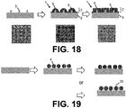
- Fig. 22 enlarges a portion of Fig. 18 and illustrates how one can determine whether a gap (21) fulfils its width and depth (d) requirements.
- the nanopillar in Fig. 22 has a width of about 35 nm and for the purpose of the present demonstration only, the figure is considered drawn to scale.
- the gap fulfils its width (w) and depth (d) requirements because a gap width (w) of 40 nm can be defined at the depicted position, and the depth (d) measured from said position to the substrate of at least 10 nm (here about 40 nm).
- the at least one position along the height of the gap is within 50 nm of the top of the surface (s).
- Fig. 23 enlarges another portion of Fig. 18 and also illustrates how one can determine whether a gap (21) fulfils its width (w) and depth (d) requirements.
- the nanopillar in Fig. 23 has a width of about 35 nm and for the purpose of the present demonstration only, the figure is considered drawn to scale. As depicted on Fig. 23 , there is a gap between two nanostructures. If the requirement is that the surface comprises gaps having a width (w), measured parallel to the substrate at at least one position along the height (h G ) of the gaps, of from of from 2 nm to 10 nm and a depth measured from said position to the substrate of at least 10 nm, whether the gaps fulfil this requirement can be determined as follows.
- the gap fulfils its width (w) and depth (d) requirements because a gap width (w) of 9 nm can be defined at the depicted position, and the depth (d) measured from said position to the substrate is of at least 10 nm (here about 55 nm).
- the at least one position along the height of the gap is within 50 nm of the top of the surface (s).
- the surface may comprise a plurality of nanostructures (4) having a width (Wh) of from 20 to 400 nm, packed in such a way that the gaps exist between adjacent nanostructures (4).
- the depth of the gaps measured toward the substrate may be at least 20 nm.
- the gaps cover from 1 to 15% of the surface.
- An alternative expression of the fourth aspect is therefore the use of a structure (1) for killing and/or inhibiting the growth of a microorganism, the structure comprising a surface (2) on a substrate (3), the surface comprising a plurality of nanostructures (4) having a width (Wh) of from 20 to 400 nm, packed in such a way that gaps exists in the surface, between nanostructures (4), said gaps having a width (w), measured parallel to the substrate at at least one position along the height (h G ) of the gaps, of from 2 nm to 400 nm, preferably from 2 to 40 nm, more preferably from 2 to 20 nm, most preferably from 2 to 10 nm and a depth (d) measured from said position to the substrate of at least 10 nm.
- the packing density of the nanostructures i.e. the proportion of the surface covered by the nanostructures (e.g. nanoparticles), is preferably at least 0.85 (the gaps cover at most 15% of the surface), preferably at least 0.90 (the gaps cover at most 10% of the surface), yet more preferably at least 0.92 (the gaps cover at most 8% of the surface).
- the close packing of spherical particles permits a maximum packing density of 0.9069 when the packing is hexagonal. However, a larger maximum packing density can be achieved when the particles adopt a more cubic shape (see surface n°5 in the examples, Fig. 18 (right) and Fig. 21 ).
- a high packing density typically translates in smaller gaps in the surface, between the nanostructures.
- Another alternative expression of the fourth aspect is therefore the use of a structure (1) for killing and/or inhibiting the growth of a microorganism, the structure comprising a surface (2) on a substrate (3), the surface comprising a plurality of nanostructures (4) having a width (Wh) of from 20 to 400 nm and having a packing density of at least 0.85, preferably at least 0.90, yet more preferably at least 0.92.
- the packing density is however smaller than 1.00.
- a packing density of 1.00 is for instance theoretically achievable with cubic nanoparticles. Such a packing density however does not present gaps susceptible to kill the microbes.
- the packing density is preferably smaller than 0.99.
- the area covered by the gaps at the at least one position along the height (h G ), may represent at least 1% of the area of the structure at that height (h G ). For instance, it may represent from 1 to 50% and more typically from 1 to 15%, from 1 to 10% or from 1 to 8% of the area of the structure at that height (parallel to the substrate).
- the area covered by the gaps, the extent of the gaps, and the packing density are measured by taking a picture of the surface from the top, and by measuring the extent of the gaps and the packing density visible on that picture.
- This is schematised in Figs. 20 and 21 where gaps between nanostructures are measured and where the area taken by the white portions of the images (particles) divided by the area taken by both the white and the black areas of the images (particles + gaps) is measured.
- the gaps measured on the picture preferably correspond in the structure to a gap situated at least 10 nm and preferably at least 20 nm above the substrate. This permits parts of the microbe to fall into the gap in a way that is detrimental for its survival.
- a diameter (i.e. a width) of 20 nm for the nanoparticles assures that the distance between the gap as measured and the substrate is 10 nm. In the case of cubic nanoparticles having a width of 20 nm, the distance between the gap as measured and the substrate is 20 nm.
- the structure, the microorganism, the surface and the substrate may be as defined in any embodiment of the first aspect.
- the structure and the surface are artefacts, i.e. they are synthetic/man made.
- the nanostructures may comprise a nanopillar and a head as in the first aspect, or not. In this last case, the nanostructures may consist in nanoparticles. These nanoparticles may have any characteristic defined for the head in the first aspect.
- the shape of the nanostructure is not very critical as long as the gaps are present. For instance, the nanoparticles may be hemispherical, spherical, cubic, cylindrical or rectangular nanoparticles amongst others.
- the surface comprising a plurality of nanoparticles can be formed on the substrate by first purchasing or synthesizing nanoparticles, then depositing them on the substrate, followed by fixing the particles on the substrate.
- the material of the nanoparticles is not critical. For instance, SiO x (e.g. SiO 2 ), Si 3 N 4 , polystyrene, or metal oxide particles can be used, amongst others.
- the particles can be monodisperse or polydisperse but are preferably monodisperse.
- Depositing the particles on the surface can be performed by a large variety of methods.
- An example is detailed in example 8 (convective assembly) but methods based on capillarity, electrostatics, the use of surfactants, or the use of molecular interactions (e.g. DNA interactions) can be used.
- An example involving self-assembling a nanoparticle monolayer at a liquid-air interface, followed by draping it over a solid substrate is disclosed in K.E. Mueggenburg et al. (Nature materials, vol.6, 09/2007, p.656-660 ).
- Fixing the particles on the substrate can be performed in various ways. One way is to heat up the substrate with the particles thereon to achieve thermal bonding. Another way is to coat the particles with a coating layer, thinner than the width of the particles and preferably thinner than half the width of the particles. A combination of both method can also be used.
- the present invention relates to a structure comprising an antimicrobial surface on a substrate, the antimicrobial surface comprising a plurality of nanoparticles having a width (Wh) of from 20 to 400 nm, packed in such a way that gaps exists in the surface, between nanoparticles, having a width (w), measured parallel to the substrate at at least one position along the height (h G ) of the gaps, of from 2 nm to 400 nm, preferably from 2 to 40 nm, more preferably from 2 to 20 nm, most preferably from 2 to 10 nm and a depth (d) measured from said position to the substrate of at least 10 nm.
- the structure further comprising a coating layer covering the nanoparticles, the coating layer being thinner than the width of the particles and preferably thinner than half the width of the particles.
- the area covered by the gaps, at the at least one position along the height (h G ), may represent at least 1% of the area of the structure at that height (h G ). For instance, it may represent from 1 to 50% and more typically from 1 to 15%, from 1 to 10% or from 1 to 8% of the area of the structure at that height (parallel to the substrate).
- the characteristics of the structure, the surface, the substrate, the nanoparticles (called head in the first aspect), the gaps, and the coating can be as defined in any embodiment of the other aspects of the present invention.
- Example 1 preparation of different nanostructured Si surfaces
- FIG. 11 Several Si surfaces each comprising differently shaped nanopillars were prepared by lithography and plasma etching (CH 2 F 2 /SF 6 /N 2 based chemistry) of Si wafers (14). This was performed by 1) providing a stack comprising a silicon substrate (14), an amorphous carbon hard mask (16) on the silicon substrate (14), an antireflective layer (17) on the hard mask (16), a positive photoresist (18) on the antireflective layer (17), 2) forming circular patterns (19) in the photoresist by immersion lithography (193 nm), the circular patterns (19) having the dimensions of the cross-section of the desired nanopillars (5), 3) transferring the circular pattern (19) into the silicon substrate (14) by dry plasma etching (CH 2 F 2 /SF 6 /N 2 based chemistry), thereby forming the nanopillars (5).
- CH 2 F 2 /SF 6 /N 2 based chemistry dry plasma etching
- round SiO 2 heads (6) were deposited on top of the nanopillars (5) by sputtering or chemical vapor deposition, thereby forming nanostructures (4) forming an antimicrobial surface (2).
- 100 nm SiO 2 was deposited on 590 nm high nanopillars by sputtering with a Pfeiffer Spider 630 sputter coater.
- a first comparative sample (“50nm Wavy”) comprised an undulating surface of nanopillars having a height of about 50 nm.
- a second comparative sample (“330nm”) comprised nanopillars having a flat top and a height of about 330 nm.
- a third comparative sample (“350nm with tips”) comprised nanopillars having a sharp tip and a height of about 350 nm.
- a fourth comparative sample (420nm), which is not shown, comprised nanopillars having a flat top and a height of about 420 nm.
- a fifth comparative sample (“580nm”) comprised nanopillars having a flat top and a height of about 580 nm.
- a sample according to an embodiment of the present invention (“590nm+100nm Q-tip”) comprised nanopillars having a round head of about 100 nm on top of a nanopillar having a height of about 590 nm.
- a sixth comparative sample (“700nm with tips”) comprised nanopillars having a sharp tip and an irregular height up to about 700 nm. It is worth noting that each of these comparative samples could serve to make embodiments of the present invention by adding a head on top of these nanopillars.
- Example 2 comparison of the different nanostructured surfaces
- Silicon and other (cf. infra) nanostructured surfaces were diced into surfaces of equal size ( ⁇ 0.8*0.8mm) and cleaned with UV light and ozone. The cleaned surfaces were packed under low pressure pure nitrogen to prevent any molecules settling down on the clean surface during transport and temporary storage.
- Escherichia coli (BW25113, Keico wild-type) and mutants with the same genetic background were used in the experiment unless otherwise stated. Bacteria were grown overnight on 37 °C on an LB agar plate. From the overnight colonies, a small lob was taken and suspended in 1.5 ml MiliQ. This suspension was adjusted to OD 595 0.3.
- the cell suspension was diluted 200 times to obtain the final inoculum.
- the inoculum had an approximated concentration in the order of 10 6 CFU/ml.
- Freshly cleaned surfaces according to the present invention were carefully put into a sterile 24-well plate (Cellstar, Greiner Bio-One) using sterilized tweezers as to not scratch and thus damage the nanoimprinted surfaces.
- the inoculum was gently vortexed and 40 ⁇ l was put on each surface. 40 ⁇ l formed a thin film which covered the entire surface. Hydrophobic surfaces would not have a film on it, as the inoculum formed a droplet on the surface, occupying a surface area dependent on the contact angle of the inoculum on the coating.
- One or more empty wells were filled with 800 ⁇ l LB as a sterility control.
- the wells were covered with sterile Breathseal Sealers (Greiner Bio-One) and the lid, after which the well plate was carefully put in a humid controlled environment to prevent evaporation as much as possible.
- the surfaces were incubated on 37 °C for the desired incubation time.
- the initial inoculum was incubated on 37 °C in a separate Eppendorf tube for the same incubation time.
- the viable cell count of the incubated initial inoculum at that time point was averaged over the different platings. This count was subtracted by the viable cell count of the surfaces and divided by the averaged viable cell count of the incubated initial inoculum of that time point. This resulted in the fraction of killed cells by which the surfaces were benchmarked.
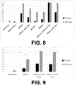
- Fig. 8 The killing efficiency of E. coli for the different nanostructured Si surfaces of example 1 and the reference is shown after 3 hours and 18 hours. Other than for the undulating surface ("50nm wavy"), a considerable killing efficiency after 18 hours is found for all nanostructured Si surfaces. Nevertheless, the nanostructured surface of the present invention (“590nm+100nm Q-tip”), comprising both pillars and heads, vastly exceeded the other surfaces by reaching 100% efficiency and this already after 3 hours.
- Example 3 preparation and comparison of nanostructured surfaces covered by an antimicrobial substance
- Si surfaces each comprising nanopillars were prepared as in example 1, the nanopillars having a flat top and a height of about 580 nm.
- a 5 nm or 10 nm HfO x layer was deposited on top of the nanopillars using atomic layer deposition.
- HfO x is known to be toxic to the E. coli bacteria.
- Fig. 9 The killing efficiency of E. coli for the fifth sample of example 1 ("580nm"), the two present samples (“580nm + 5nm HfOx” and “580nm + 10nm HfOx”) and the reference is shown after 3 hours and 18 hours. It was observed that coating the nanopillars in the toxic substance further increased their efficiency, with an increase in efficiency after 18 hours from about 50% to over 80%.
- Example 4 preparation and comparison of nanostructured surfaces based on block copolymers
- FIG. 14 A polystyrene- block -poly(methyl methacrylate) (PS- b -PMMA) block copolymer layer (11) was phase separated into a PS cylindrical phase (12) and a PMMA phase, and the PMMA non-cylindrical phase was removed, leaving cylindrical PS nanopillars (5) on a substrate (3), the nanopillars (5) having a height of about 40 nm and a width of about 20 to 25 nm (see Fig. 7 left).
- PS- b -PMMA poly(methyl methacrylate)
- AlO x is also known to be toxic to E. coli.
- FIG. 10 The killing efficiency of E. coli for the PS nanopillared surface ("40nm PS"), the AlO x nanopillared surface ("120nm AlOx D20”) and the reference is shown after 3 hours and 18 hours. It was observed that these alternative nanostructured surfaces, i.e. based on organic materials, can also be effective. For the PS nanopillared surface a moderate killing efficiency is found, which is nevertheless fairly substantial when compared to the undulating surface of example 1 having a similar height ("50nm Wavy"). For the AlO x nanopillared surface, comprising the toxic AlO x , a very good efficiency of 100% is found after 18 hours.
- Example 5 preparation of seven further nanostructured Si surfaces
- nanostructured surfaces have been prepared by procedures analogous to example 1. All of these nanostructured surfaces comprised a square matrix of regularly spaced nanopillars. The center to center distance between nanopillars along a row or a column of the matrix was 90 nm. Each nanopillar had a regular width of 35 nm. Three of these surfaces comprised nanopillars but no heads. Surface n°1 had nanopillars that were 50 nm high (see Fig. 15 left and 18 left), Surface n°2 had nanopillars that were 330 nm high (see Fig. 16 left) and surface n°3 had nanopillars that were 700 nm high. Four others of these surfaces comprised nanopillars on which a SiO 2 head had been sputtered.
- n°4 had nanopillars that were 50 nm high and had a 90 nm thick SiO 2 layer sputtered thereon, thereby forming a hemispherical head covering the top of the nanopillars and their entire height (see Fig. 18 center).
- Surface n°5 had nanopillars that were 50 nm high and had a 130 nm thick SiO 2 layer sputtered thereon (see Fig. 15 right, Fig. 18 right and Fig. 21 ), thereby forming a square shaped head covering the top of the nanopillars and their entire height. The space between the heads was smaller than in the case of the hemispherical heads.
- Surface n°6 (see Fig.
- Fig. 20 schematized a top view of an antimicrobial surface comprising a plurality of nanostructures (4).
- Such a top view represents schematically the situation of Surfaces n°4, 6, and 7.
- the double arrow shows a gap existing between two adjacent nanostructures. Due to the close-packing, such a gap in small enough to impart antimicrobial activity to the surface.
- Fig. 21 schematized a top view of an antimicrobial surface comprising a plurality of nanostructures (4).
- Such a top view represents schematically the situation of Surface n°5.
- the double arrow shows a gap existing between two adjacent nanostructures. Due to the close-packing and the thicker SiO 2 layer deposited on the nanopillars, such a gap in smaller than when a thinner SiO 2 layer is deposited (situation of Surface n°4). This imparts to surface n°5 enhanced antimicrobial activity to the surface comparted to Surface n°4.
- Example 6 comparison of the nanostructured surfaces of example 5 with nanostructures obtained in example 1.
- the microbial surfaces and the cell suspensions were prepared as in example 2. Incubating of the surfaces, plating, counting, and efficiency calculations were also performed as in example 2. In addition to E. coli, S. aureus and mutants with the same genetic background have also been tested with similar results (not depicted in the figures).
- FIG. 17 The killing efficiency of E. coli for Surfaces 1 to 7, for the reference, and the reference coated with 100 nm SiO 2 (reference + SiOx), The killing efficiency for each surface are shown after 3 hours and 18 hours in contact with the bacteria. It can be observed that other than for the reference, the reference coated with SiO 2 (reference + SiOx), and surface 1 (50 nm), a considerable killing efficiency after 18 hours is found for Surfaces 2-7. Nevertheless, the nanostructured surface of the present invention (Surfaces 4-7) comprising a head, vastly exceeded the other surfaces by reaching 100% efficiency and this already after 3 hours.
- Example 7 Varying the amount of SiO 2 sputtered on Surface 1 or Example 5.
- Example 8 Formation of antimicrobial surfaces by close-packing nanoparticles.
- Polystyrene particles (4) with a 499 ⁇ 5 nm diameter purchased from Duke Scientific (Palo Alto, CA), are deposited on a PDMS substrate treated with an oxygen plasma by convective assembly, as disclosed in L. Malaquin et al. (Langmuir 2007, 23, 11513-11521 ), thereby obtaining a closely packed assembly of particles. These particles are then fixed to the substrate by either thermal bonding (top) or by applying a coating (20) on the particles (bottom).
- SiO 2 nanospheres of sizes 50, 80, 100, 120, and 140 nm purchased from Sigma-Aldrich.
- Si 3 N 4 spherical particles of sizes 50, 1000, and 10000 nm purchased from Sigma-Aldrich.
- iron oxide nanoparticles with a diameter in the range 50-100 nm purchased from Sigma-Aldrich.
- Example 9 Testing of the antimicrobial properties of the samples of example 8.
- Example 2 is repeated on the antimicrobial surfaces obtained in example 8.
Landscapes
- Life Sciences & Earth Sciences (AREA)
- Engineering & Computer Science (AREA)
- Health & Medical Sciences (AREA)
- General Health & Medical Sciences (AREA)
- Chemical & Material Sciences (AREA)
- Manufacturing & Machinery (AREA)
- Plant Pathology (AREA)
- Wood Science & Technology (AREA)
- Environmental Sciences (AREA)
- Zoology (AREA)
- Dentistry (AREA)
- Pest Control & Pesticides (AREA)
- Agronomy & Crop Science (AREA)
- Toxicology (AREA)
- Nanotechnology (AREA)
- Crystallography & Structural Chemistry (AREA)
- Molecular Biology (AREA)
- Microelectronics & Electronic Packaging (AREA)
- Medicinal Chemistry (AREA)
- Polymers & Plastics (AREA)
- Organic Chemistry (AREA)
- Chemical Kinetics & Catalysis (AREA)
- Inorganic Chemistry (AREA)
- Apparatus For Disinfection Or Sterilisation (AREA)
- Materials For Medical Uses (AREA)
- Physics & Mathematics (AREA)
- Plasma & Fusion (AREA)
- Agricultural Chemicals And Associated Chemicals (AREA)
Applications Claiming Priority (2)
| Application Number | Priority Date | Filing Date | Title |
|---|---|---|---|
| EP17153880 | 2017-01-31 | ||
| EP17170193 | 2017-05-09 |
Publications (3)
| Publication Number | Publication Date |
|---|---|
| EP3354136A2 true EP3354136A2 (de) | 2018-08-01 |
| EP3354136A3 EP3354136A3 (de) | 2018-08-22 |
| EP3354136B1 EP3354136B1 (de) | 2020-05-13 |
Family
ID=60972100
Family Applications (1)
| Application Number | Title | Priority Date | Filing Date |
|---|---|---|---|
| EP18151541.2A Active EP3354136B1 (de) | 2017-01-31 | 2018-01-15 | Antimikrobielle substratoberfläche |
Country Status (2)
| Country | Link |
|---|---|
| US (1) | US10433542B2 (de) |
| EP (1) | EP3354136B1 (de) |
Families Citing this family (6)
| Publication number | Priority date | Publication date | Assignee | Title |
|---|---|---|---|---|
| US11785943B2 (en) * | 2017-09-22 | 2023-10-17 | Uchicago Argonne, Llc | Tunable nanotextured materials |
| US11038011B2 (en) * | 2019-10-29 | 2021-06-15 | Globalfoundries U.S. Inc. | Metal-insulator-metal capacitors including nanofibers |
| WO2022076343A1 (en) * | 2020-10-06 | 2022-04-14 | F9 Llc | Antimicrobial metal powders and related materials |
| MC200246B1 (fr) * | 2021-06-10 | 2022-07-18 | Mitchell Newdelman | Composition et dispositif pour la desinfection de l'air |
| EP4379397B1 (de) | 2022-11-30 | 2026-03-18 | Imec VZW | Verfahren zur herstellung eines substrats mit mehreren spitzen für die rastersondenmikroskopie |
| CN117208840A (zh) * | 2023-08-11 | 2023-12-12 | 哈尔滨工业大学(深圳)(哈尔滨工业大学深圳科技创新研究院) | 一种具有宽谱抗菌性的表面微纳结构及其制造方法 |
Citations (1)
| Publication number | Priority date | Publication date | Assignee | Title |
|---|---|---|---|---|
| WO2015031956A1 (en) | 2013-09-05 | 2015-03-12 | Swinburne University Of Technology | A synthetic biocidal surface comprising an array of nanospikes |
Family Cites Families (2)
| Publication number | Priority date | Publication date | Assignee | Title |
|---|---|---|---|---|
| CN104380084A (zh) * | 2012-04-10 | 2015-02-25 | 普林斯顿大学理事会 | 超灵敏传感器 |
| US10875235B2 (en) * | 2014-04-01 | 2020-12-29 | The Regents Of The University Of California | Bactericidal surface patterns |
-
2018
- 2018-01-15 US US15/871,190 patent/US10433542B2/en active Active
- 2018-01-15 EP EP18151541.2A patent/EP3354136B1/de active Active
Patent Citations (1)
| Publication number | Priority date | Publication date | Assignee | Title |
|---|---|---|---|---|
| WO2015031956A1 (en) | 2013-09-05 | 2015-03-12 | Swinburne University Of Technology | A synthetic biocidal surface comprising an array of nanospikes |
Non-Patent Citations (2)
| Title |
|---|
| K.E. MUEGGENBURG ET AL., NATURE MATERIALS, vol. 6, September 2007 (2007-09-01), pages 656 - 660 |
| MALAQUIN ET AL., LANGMUIR, vol. 23, 2007, pages 11513 - 11521 |
Also Published As
| Publication number | Publication date |
|---|---|
| EP3354136A3 (de) | 2018-08-22 |
| EP3354136B1 (de) | 2020-05-13 |
| US10433542B2 (en) | 2019-10-08 |
| US20180213772A1 (en) | 2018-08-02 |
Similar Documents
| Publication | Publication Date | Title |
|---|---|---|
| US10433542B2 (en) | Antimicrobial substrate surface | |
| Hazell et al. | Studies of black silicon and black diamond as materials for antibacterial surfaces | |
| ES2778173T3 (es) | Una superficie biocida sintética que comprende un conjunto de nanopuntas | |
| Hizal et al. | Nanoengineered superhydrophobic surfaces of aluminum with extremely low bacterial adhesivity | |
| Jiang et al. | Lotus-leaf-inspired hierarchical structured surface with non-fouling and mechanical bactericidal performances | |
| Sengstock et al. | Structure-related antibacterial activity of a titanium nanostructured surface fabricated by glancing angle sputter deposition | |
| Yang et al. | Control of bacterial adhesion and growth on honeycomb-like patterned surfaces | |
| Li et al. | The nanotipped hairs of gecko skin and biotemplated replicas impair and/or kill pathogenic bacteria with high efficiency | |
| Wang et al. | Microenvironment-responsive magnetic nanocomposites based on silver nanoparticles/gentamicin for enhanced biofilm disruption by magnetic field | |
| Epstein et al. | Control of bacterial biofilm growth on surfaces by nanostructural mechanics and geometry | |
| Huo et al. | Osteogenic activity and antibacterial effects on titanium surfaces modified with Zn-incorporated nanotube arrays | |
| Seyfi et al. | Developing antibacterial superhydrophobic coatings based on polydimethylsiloxane/silver phosphate nanocomposites: assessment of surface morphology, roughness and chemistry | |
| JP6516662B2 (ja) | 殺菌作用を有するフィルターを用いた殺菌方法 | |
| Han et al. | Superhydrophilic nanopillar-structured quartz surfaces for the prevention of biofilm formation in optical devices | |
| Dong et al. | Zinc oxide superstructures in colloidal polymer nanocomposite films: Enhanced antibacterial activity through slow drying | |
| Nikiforov et al. | Plasma technology in antimicrobial surface engineering | |
| Uhm et al. | Tailoring of antibacterial Ag nanostructures on TiO2 nanotube layers by magnetron sputtering | |
| Kruszewski et al. | Reducing Staphylococcus aureus biofilm formation on stainless steel 316L using functionalized self-assembled monolayers | |
| Song et al. | pH-responsive smart wettability surface with dual bactericidal and releasing properties | |
| Unosson et al. | Reactive combinatorial synthesis and characterization of a gradient Ag–Ti oxide thin film with antibacterial properties | |
| Baburova et al. | Magnetic soft robot for minimally invasive urethral catheter biofilm eradication | |
| Li et al. | A nanostructured anti-biofilm surface widens the efficacy against spindle-shaped and chain-forming rod-like bacteria | |
| US9321030B2 (en) | Clay-containing thin films as carriers of absorbed molecules | |
| Susarrey-Arce et al. | Bacterial viability on chemically modified silicon nanowire arrays | |
| Wu et al. | Electric assisted salt-responsive bacterial killing and release of polyzwitterionic brushes in low-concentration salt solution |
Legal Events
| Date | Code | Title | Description |
|---|---|---|---|
| PUAI | Public reference made under article 153(3) epc to a published international application that has entered the european phase |
Free format text: ORIGINAL CODE: 0009012 |
|
| STAA | Information on the status of an ep patent application or granted ep patent |
Free format text: STATUS: THE APPLICATION HAS BEEN PUBLISHED |
|
| PUAL | Search report despatched |
Free format text: ORIGINAL CODE: 0009013 |
|
| AK | Designated contracting states |
Kind code of ref document: A2 Designated state(s): AL AT BE BG CH CY CZ DE DK EE ES FI FR GB GR HR HU IE IS IT LI LT LU LV MC MK MT NL NO PL PT RO RS SE SI SK SM TR |
|
| AX | Request for extension of the european patent |
Extension state: BA ME |
|
| AK | Designated contracting states |
Kind code of ref document: A3 Designated state(s): AL AT BE BG CH CY CZ DE DK EE ES FI FR GB GR HR HU IE IS IT LI LT LU LV MC MK MT NL NO PL PT RO RS SE SI SK SM TR |
|
| AX | Request for extension of the european patent |
Extension state: BA ME |
|
| RIC1 | Information provided on ipc code assigned before grant |
Ipc: B82Y 40/00 20110101ALI20180719BHEP Ipc: B82B 3/00 20060101ALI20180719BHEP Ipc: H01L 21/3065 20060101ALI20180719BHEP Ipc: A01N 25/34 20060101AFI20180719BHEP |
|
| STAA | Information on the status of an ep patent application or granted ep patent |
Free format text: STATUS: REQUEST FOR EXAMINATION WAS MADE |
|
| 17P | Request for examination filed |
Effective date: 20190219 |
|
| RBV | Designated contracting states (corrected) |
Designated state(s): AL AT BE BG CH CY CZ DE DK EE ES FI FR GB GR HR HU IE IS IT LI LT LU LV MC MK MT NL NO PL PT RO RS SE SI SK SM TR |
|
| GRAP | Despatch of communication of intention to grant a patent |
Free format text: ORIGINAL CODE: EPIDOSNIGR1 |
|
| RIC1 | Information provided on ipc code assigned before grant |
Ipc: H01L 21/3065 20060101ALI20191213BHEP Ipc: A01P 1/00 20060101ALI20191213BHEP Ipc: B82Y 30/00 20110101ALI20191213BHEP Ipc: A01N 25/34 20060101AFI20191213BHEP Ipc: B82Y 40/00 20110101ALI20191213BHEP Ipc: B82B 3/00 20060101ALI20191213BHEP Ipc: B81C 1/00 20060101ALI20191213BHEP |
|
| STAA | Information on the status of an ep patent application or granted ep patent |
Free format text: STATUS: GRANT OF PATENT IS INTENDED |
|
| INTG | Intention to grant announced |
Effective date: 20200123 |
|
| GRAS | Grant fee paid |
Free format text: ORIGINAL CODE: EPIDOSNIGR3 |
|
| GRAA | (expected) grant |
Free format text: ORIGINAL CODE: 0009210 |
|
| STAA | Information on the status of an ep patent application or granted ep patent |
Free format text: STATUS: THE PATENT HAS BEEN GRANTED |
|
| AK | Designated contracting states |
Kind code of ref document: B1 Designated state(s): AL AT BE BG CH CY CZ DE DK EE ES FI FR GB GR HR HU IE IS IT LI LT LU LV MC MK MT NL NO PL PT RO RS SE SI SK SM TR |
|
| REG | Reference to a national code |
Ref country code: GB Ref legal event code: FG4D |
|
| REG | Reference to a national code |
Ref country code: CH Ref legal event code: EP |
|
| REG | Reference to a national code |
Ref country code: DE Ref legal event code: R096 Ref document number: 602018004248 Country of ref document: DE |
|
| REG | Reference to a national code |
Ref country code: AT Ref legal event code: REF Ref document number: 1269007 Country of ref document: AT Kind code of ref document: T Effective date: 20200615 |
|
| REG | Reference to a national code |
Ref country code: LT Ref legal event code: MG4D |
|
| REG | Reference to a national code |
Ref country code: NL Ref legal event code: MP Effective date: 20200513 |
|
| PG25 | Lapsed in a contracting state [announced via postgrant information from national office to epo] |
Ref country code: LT Free format text: LAPSE BECAUSE OF FAILURE TO SUBMIT A TRANSLATION OF THE DESCRIPTION OR TO PAY THE FEE WITHIN THE PRESCRIBED TIME-LIMIT Effective date: 20200513 Ref country code: FI Free format text: LAPSE BECAUSE OF FAILURE TO SUBMIT A TRANSLATION OF THE DESCRIPTION OR TO PAY THE FEE WITHIN THE PRESCRIBED TIME-LIMIT Effective date: 20200513 Ref country code: SE Free format text: LAPSE BECAUSE OF FAILURE TO SUBMIT A TRANSLATION OF THE DESCRIPTION OR TO PAY THE FEE WITHIN THE PRESCRIBED TIME-LIMIT Effective date: 20200513 Ref country code: PT Free format text: LAPSE BECAUSE OF FAILURE TO SUBMIT A TRANSLATION OF THE DESCRIPTION OR TO PAY THE FEE WITHIN THE PRESCRIBED TIME-LIMIT Effective date: 20200914 Ref country code: IS Free format text: LAPSE BECAUSE OF FAILURE TO SUBMIT A TRANSLATION OF THE DESCRIPTION OR TO PAY THE FEE WITHIN THE PRESCRIBED TIME-LIMIT Effective date: 20200913 Ref country code: GR Free format text: LAPSE BECAUSE OF FAILURE TO SUBMIT A TRANSLATION OF THE DESCRIPTION OR TO PAY THE FEE WITHIN THE PRESCRIBED TIME-LIMIT Effective date: 20200814 Ref country code: NO Free format text: LAPSE BECAUSE OF FAILURE TO SUBMIT A TRANSLATION OF THE DESCRIPTION OR TO PAY THE FEE WITHIN THE PRESCRIBED TIME-LIMIT Effective date: 20200813 |
|
| PG25 | Lapsed in a contracting state [announced via postgrant information from national office to epo] |
Ref country code: RS Free format text: LAPSE BECAUSE OF FAILURE TO SUBMIT A TRANSLATION OF THE DESCRIPTION OR TO PAY THE FEE WITHIN THE PRESCRIBED TIME-LIMIT Effective date: 20200513 Ref country code: LV Free format text: LAPSE BECAUSE OF FAILURE TO SUBMIT A TRANSLATION OF THE DESCRIPTION OR TO PAY THE FEE WITHIN THE PRESCRIBED TIME-LIMIT Effective date: 20200513 Ref country code: BG Free format text: LAPSE BECAUSE OF FAILURE TO SUBMIT A TRANSLATION OF THE DESCRIPTION OR TO PAY THE FEE WITHIN THE PRESCRIBED TIME-LIMIT Effective date: 20200813 Ref country code: HR Free format text: LAPSE BECAUSE OF FAILURE TO SUBMIT A TRANSLATION OF THE DESCRIPTION OR TO PAY THE FEE WITHIN THE PRESCRIBED TIME-LIMIT Effective date: 20200513 |
|
| REG | Reference to a national code |
Ref country code: AT Ref legal event code: MK05 Ref document number: 1269007 Country of ref document: AT Kind code of ref document: T Effective date: 20200513 |
|
| PG25 | Lapsed in a contracting state [announced via postgrant information from national office to epo] |
Ref country code: AL Free format text: LAPSE BECAUSE OF FAILURE TO SUBMIT A TRANSLATION OF THE DESCRIPTION OR TO PAY THE FEE WITHIN THE PRESCRIBED TIME-LIMIT Effective date: 20200513 Ref country code: NL Free format text: LAPSE BECAUSE OF FAILURE TO SUBMIT A TRANSLATION OF THE DESCRIPTION OR TO PAY THE FEE WITHIN THE PRESCRIBED TIME-LIMIT Effective date: 20200513 |
|
| PG25 | Lapsed in a contracting state [announced via postgrant information from national office to epo] |
Ref country code: IT Free format text: LAPSE BECAUSE OF FAILURE TO SUBMIT A TRANSLATION OF THE DESCRIPTION OR TO PAY THE FEE WITHIN THE PRESCRIBED TIME-LIMIT Effective date: 20200513 Ref country code: AT Free format text: LAPSE BECAUSE OF FAILURE TO SUBMIT A TRANSLATION OF THE DESCRIPTION OR TO PAY THE FEE WITHIN THE PRESCRIBED TIME-LIMIT Effective date: 20200513 Ref country code: DK Free format text: LAPSE BECAUSE OF FAILURE TO SUBMIT A TRANSLATION OF THE DESCRIPTION OR TO PAY THE FEE WITHIN THE PRESCRIBED TIME-LIMIT Effective date: 20200513 Ref country code: ES Free format text: LAPSE BECAUSE OF FAILURE TO SUBMIT A TRANSLATION OF THE DESCRIPTION OR TO PAY THE FEE WITHIN THE PRESCRIBED TIME-LIMIT Effective date: 20200513 Ref country code: RO Free format text: LAPSE BECAUSE OF FAILURE TO SUBMIT A TRANSLATION OF THE DESCRIPTION OR TO PAY THE FEE WITHIN THE PRESCRIBED TIME-LIMIT Effective date: 20200513 Ref country code: CZ Free format text: LAPSE BECAUSE OF FAILURE TO SUBMIT A TRANSLATION OF THE DESCRIPTION OR TO PAY THE FEE WITHIN THE PRESCRIBED TIME-LIMIT Effective date: 20200513 Ref country code: EE Free format text: LAPSE BECAUSE OF FAILURE TO SUBMIT A TRANSLATION OF THE DESCRIPTION OR TO PAY THE FEE WITHIN THE PRESCRIBED TIME-LIMIT Effective date: 20200513 Ref country code: SM Free format text: LAPSE BECAUSE OF FAILURE TO SUBMIT A TRANSLATION OF THE DESCRIPTION OR TO PAY THE FEE WITHIN THE PRESCRIBED TIME-LIMIT Effective date: 20200513 |
|
| REG | Reference to a national code |
Ref country code: DE Ref legal event code: R097 Ref document number: 602018004248 Country of ref document: DE |
|
| PG25 | Lapsed in a contracting state [announced via postgrant information from national office to epo] |
Ref country code: SK Free format text: LAPSE BECAUSE OF FAILURE TO SUBMIT A TRANSLATION OF THE DESCRIPTION OR TO PAY THE FEE WITHIN THE PRESCRIBED TIME-LIMIT Effective date: 20200513 Ref country code: PL Free format text: LAPSE BECAUSE OF FAILURE TO SUBMIT A TRANSLATION OF THE DESCRIPTION OR TO PAY THE FEE WITHIN THE PRESCRIBED TIME-LIMIT Effective date: 20200513 |
|
| PLBE | No opposition filed within time limit |
Free format text: ORIGINAL CODE: 0009261 |
|
| STAA | Information on the status of an ep patent application or granted ep patent |
Free format text: STATUS: NO OPPOSITION FILED WITHIN TIME LIMIT |
|
| 26N | No opposition filed |
Effective date: 20210216 |
|
| PG25 | Lapsed in a contracting state [announced via postgrant information from national office to epo] |
Ref country code: SI Free format text: LAPSE BECAUSE OF FAILURE TO SUBMIT A TRANSLATION OF THE DESCRIPTION OR TO PAY THE FEE WITHIN THE PRESCRIBED TIME-LIMIT Effective date: 20200513 |
|
| PG25 | Lapsed in a contracting state [announced via postgrant information from national office to epo] |
Ref country code: MC Free format text: LAPSE BECAUSE OF FAILURE TO SUBMIT A TRANSLATION OF THE DESCRIPTION OR TO PAY THE FEE WITHIN THE PRESCRIBED TIME-LIMIT Effective date: 20200513 |
|
| PG25 | Lapsed in a contracting state [announced via postgrant information from national office to epo] |
Ref country code: LU Free format text: LAPSE BECAUSE OF NON-PAYMENT OF DUE FEES Effective date: 20210115 |
|
| REG | Reference to a national code |
Ref country code: BE Ref legal event code: MM Effective date: 20210131 |
|
| PG25 | Lapsed in a contracting state [announced via postgrant information from national office to epo] |
Ref country code: FR Free format text: LAPSE BECAUSE OF NON-PAYMENT OF DUE FEES Effective date: 20210131 |
|
| PG25 | Lapsed in a contracting state [announced via postgrant information from national office to epo] |
Ref country code: IE Free format text: LAPSE BECAUSE OF NON-PAYMENT OF DUE FEES Effective date: 20210115 |
|
| PG25 | Lapsed in a contracting state [announced via postgrant information from national office to epo] |
Ref country code: BE Free format text: LAPSE BECAUSE OF NON-PAYMENT OF DUE FEES Effective date: 20210131 |
|
| GBPC | Gb: european patent ceased through non-payment of renewal fee |
Effective date: 20220115 |
|
| PG25 | Lapsed in a contracting state [announced via postgrant information from national office to epo] |
Ref country code: GB Free format text: LAPSE BECAUSE OF NON-PAYMENT OF DUE FEES Effective date: 20220115 |
|
| P01 | Opt-out of the competence of the unified patent court (upc) registered |
Effective date: 20230513 |
|
| PG25 | Lapsed in a contracting state [announced via postgrant information from national office to epo] |
Ref country code: CY Free format text: LAPSE BECAUSE OF FAILURE TO SUBMIT A TRANSLATION OF THE DESCRIPTION OR TO PAY THE FEE WITHIN THE PRESCRIBED TIME-LIMIT Effective date: 20200513 |
|
| PG25 | Lapsed in a contracting state [announced via postgrant information from national office to epo] |
Ref country code: HU Free format text: LAPSE BECAUSE OF FAILURE TO SUBMIT A TRANSLATION OF THE DESCRIPTION OR TO PAY THE FEE WITHIN THE PRESCRIBED TIME-LIMIT; INVALID AB INITIO Effective date: 20180115 |
|
| PG25 | Lapsed in a contracting state [announced via postgrant information from national office to epo] |
Ref country code: MK Free format text: LAPSE BECAUSE OF FAILURE TO SUBMIT A TRANSLATION OF THE DESCRIPTION OR TO PAY THE FEE WITHIN THE PRESCRIBED TIME-LIMIT Effective date: 20200513 |
|
| PG25 | Lapsed in a contracting state [announced via postgrant information from national office to epo] |
Ref country code: MT Free format text: LAPSE BECAUSE OF FAILURE TO SUBMIT A TRANSLATION OF THE DESCRIPTION OR TO PAY THE FEE WITHIN THE PRESCRIBED TIME-LIMIT Effective date: 20200513 |
|
| PG25 | Lapsed in a contracting state [announced via postgrant information from national office to epo] |
Ref country code: TR Free format text: LAPSE BECAUSE OF FAILURE TO SUBMIT A TRANSLATION OF THE DESCRIPTION OR TO PAY THE FEE WITHIN THE PRESCRIBED TIME-LIMIT Effective date: 20200513 |
|
| REG | Reference to a national code |
Ref country code: CH Ref legal event code: U11 Free format text: ST27 STATUS EVENT CODE: U-0-0-U10-U11 (AS PROVIDED BY THE NATIONAL OFFICE) Effective date: 20260201 |
|
| PGFP | Annual fee paid to national office [announced via postgrant information from national office to epo] |
Ref country code: DE Payment date: 20251217 Year of fee payment: 9 |
|
| PGFP | Annual fee paid to national office [announced via postgrant information from national office to epo] |
Ref country code: CH Payment date: 20260201 Year of fee payment: 9 |