EP3353579B1 - Flexible optical fiber coupler array - Google Patents
Flexible optical fiber coupler array Download PDFInfo
- Publication number
- EP3353579B1 EP3353579B1 EP16849541.4A EP16849541A EP3353579B1 EP 3353579 B1 EP3353579 B1 EP 3353579B1 EP 16849541 A EP16849541 A EP 16849541A EP 3353579 B1 EP3353579 B1 EP 3353579B1
- Authority
- EP
- European Patent Office
- Prior art keywords
- optical
- coupler array
- waveguide
- optical fiber
- waveguides
- Prior art date
- Legal status (The legal status is an assumption and is not a legal conclusion. Google has not performed a legal analysis and makes no representation as to the accuracy of the status listed.)
- Active
Links
- 239000013307 optical fiber Substances 0.000 title claims description 156
- 230000003287 optical effect Effects 0.000 claims description 169
- 239000000835 fiber Substances 0.000 claims description 53
- 230000010287 polarization Effects 0.000 claims description 48
- 238000005253 cladding Methods 0.000 claims description 30
- 235000012239 silicon dioxide Nutrition 0.000 claims description 3
- 238000010168 coupling process Methods 0.000 description 47
- 238000005859 coupling reaction Methods 0.000 description 47
- 230000008878 coupling Effects 0.000 description 43
- 238000010586 diagram Methods 0.000 description 24
- 238000003491 array Methods 0.000 description 16
- 239000000463 material Substances 0.000 description 16
- 238000005086 pumping Methods 0.000 description 15
- 230000001965 increasing effect Effects 0.000 description 12
- 238000013461 design Methods 0.000 description 11
- 238000004519 manufacturing process Methods 0.000 description 6
- 238000000034 method Methods 0.000 description 6
- 238000004806 packaging method and process Methods 0.000 description 6
- 239000011521 glass Substances 0.000 description 5
- 230000000007 visual effect Effects 0.000 description 5
- 238000013459 approach Methods 0.000 description 4
- 230000009467 reduction Effects 0.000 description 4
- 238000005452 bending Methods 0.000 description 3
- 230000007613 environmental effect Effects 0.000 description 3
- 230000004927 fusion Effects 0.000 description 3
- 238000002955 isolation Methods 0.000 description 3
- 230000008569 process Effects 0.000 description 3
- 230000035939 shock Effects 0.000 description 3
- VYPSYNLAJGMNEJ-UHFFFAOYSA-N Silicium dioxide Chemical compound O=[Si]=O VYPSYNLAJGMNEJ-UHFFFAOYSA-N 0.000 description 2
- 238000000149 argon plasma sintering Methods 0.000 description 2
- 239000002131 composite material Substances 0.000 description 2
- 230000003247 decreasing effect Effects 0.000 description 2
- 238000007689 inspection Methods 0.000 description 2
- 238000012986 modification Methods 0.000 description 2
- 230000004048 modification Effects 0.000 description 2
- 238000005457 optimization Methods 0.000 description 2
- 230000003595 spectral effect Effects 0.000 description 2
- 230000005540 biological transmission Effects 0.000 description 1
- 239000011248 coating agent Substances 0.000 description 1
- 238000000576 coating method Methods 0.000 description 1
- 230000001427 coherent effect Effects 0.000 description 1
- 238000004891 communication Methods 0.000 description 1
- 230000002860 competitive effect Effects 0.000 description 1
- 238000011109 contamination Methods 0.000 description 1
- 238000005520 cutting process Methods 0.000 description 1
- 230000007423 decrease Effects 0.000 description 1
- 230000001419 dependent effect Effects 0.000 description 1
- 238000001514 detection method Methods 0.000 description 1
- 238000009792 diffusion process Methods 0.000 description 1
- 239000002019 doping agent Substances 0.000 description 1
- 238000005516 engineering process Methods 0.000 description 1
- 238000005530 etching Methods 0.000 description 1
- 238000007526 fusion splicing Methods 0.000 description 1
- 230000001939 inductive effect Effects 0.000 description 1
- 238000003780 insertion Methods 0.000 description 1
- 230000037431 insertion Effects 0.000 description 1
- 238000012423 maintenance Methods 0.000 description 1
- 239000003550 marker Substances 0.000 description 1
- 239000013028 medium composition Substances 0.000 description 1
- 239000004038 photonic crystal Substances 0.000 description 1
- 238000012545 processing Methods 0.000 description 1
- 230000035755 proliferation Effects 0.000 description 1
- 230000001902 propagating effect Effects 0.000 description 1
- 230000008054 signal transmission Effects 0.000 description 1
- 239000000377 silicon dioxide Substances 0.000 description 1
- 230000007480 spreading Effects 0.000 description 1
- 238000003892 spreading Methods 0.000 description 1
- 230000007704 transition Effects 0.000 description 1
Images


Classifications
-
- G—PHYSICS
- G02—OPTICS
- G02B—OPTICAL ELEMENTS, SYSTEMS OR APPARATUS
- G02B6/00—Light guides; Structural details of arrangements comprising light guides and other optical elements, e.g. couplings
- G02B6/24—Coupling light guides
- G02B6/26—Optical coupling means
- G02B6/30—Optical coupling means for use between fibre and thin-film device
-
- G—PHYSICS
- G02—OPTICS
- G02B—OPTICAL ELEMENTS, SYSTEMS OR APPARATUS
- G02B6/00—Light guides; Structural details of arrangements comprising light guides and other optical elements, e.g. couplings
- G02B6/04—Light guides; Structural details of arrangements comprising light guides and other optical elements, e.g. couplings formed by bundles of fibres
-
- G—PHYSICS
- G02—OPTICS
- G02B—OPTICAL ELEMENTS, SYSTEMS OR APPARATUS
- G02B6/00—Light guides; Structural details of arrangements comprising light guides and other optical elements, e.g. couplings
- G02B6/10—Light guides; Structural details of arrangements comprising light guides and other optical elements, e.g. couplings of the optical waveguide type
- G02B6/12—Light guides; Structural details of arrangements comprising light guides and other optical elements, e.g. couplings of the optical waveguide type of the integrated circuit kind
-
- G—PHYSICS
- G02—OPTICS
- G02B—OPTICAL ELEMENTS, SYSTEMS OR APPARATUS
- G02B6/00—Light guides; Structural details of arrangements comprising light guides and other optical elements, e.g. couplings
- G02B6/24—Coupling light guides
- G02B6/26—Optical coupling means
-
- G—PHYSICS
- G02—OPTICS
- G02B—OPTICAL ELEMENTS, SYSTEMS OR APPARATUS
- G02B6/00—Light guides; Structural details of arrangements comprising light guides and other optical elements, e.g. couplings
- G02B6/24—Coupling light guides
- G02B6/26—Optical coupling means
- G02B6/32—Optical coupling means having lens focusing means positioned between opposed fibre ends
-
- G—PHYSICS
- G02—OPTICS
- G02B—OPTICAL ELEMENTS, SYSTEMS OR APPARATUS
- G02B6/00—Light guides; Structural details of arrangements comprising light guides and other optical elements, e.g. couplings
- G02B6/10—Light guides; Structural details of arrangements comprising light guides and other optical elements, e.g. couplings of the optical waveguide type
- G02B6/12—Light guides; Structural details of arrangements comprising light guides and other optical elements, e.g. couplings of the optical waveguide type of the integrated circuit kind
- G02B2006/12035—Materials
- G02B2006/12038—Glass (SiO2 based materials)
-
- G—PHYSICS
- G02—OPTICS
- G02B—OPTICAL ELEMENTS, SYSTEMS OR APPARATUS
- G02B6/00—Light guides; Structural details of arrangements comprising light guides and other optical elements, e.g. couplings
- G02B6/10—Light guides; Structural details of arrangements comprising light guides and other optical elements, e.g. couplings of the optical waveguide type
- G02B6/12—Light guides; Structural details of arrangements comprising light guides and other optical elements, e.g. couplings of the optical waveguide type of the integrated circuit kind
- G02B2006/12133—Functions
- G02B2006/12147—Coupler
-
- G—PHYSICS
- G02—OPTICS
- G02B—OPTICAL ELEMENTS, SYSTEMS OR APPARATUS
- G02B6/00—Light guides; Structural details of arrangements comprising light guides and other optical elements, e.g. couplings
- G02B6/02—Optical fibres with cladding with or without a coating
- G02B6/02042—Multicore optical fibres
-
- G—PHYSICS
- G02—OPTICS
- G02B—OPTICAL ELEMENTS, SYSTEMS OR APPARATUS
- G02B6/00—Light guides; Structural details of arrangements comprising light guides and other optical elements, e.g. couplings
- G02B6/02—Optical fibres with cladding with or without a coating
- G02B6/024—Optical fibres with cladding with or without a coating with polarisation maintaining properties
-
- G—PHYSICS
- G02—OPTICS
- G02B—OPTICAL ELEMENTS, SYSTEMS OR APPARATUS
- G02B6/00—Light guides; Structural details of arrangements comprising light guides and other optical elements, e.g. couplings
- G02B6/10—Light guides; Structural details of arrangements comprising light guides and other optical elements, e.g. couplings of the optical waveguide type
- G02B6/12—Light guides; Structural details of arrangements comprising light guides and other optical elements, e.g. couplings of the optical waveguide type of the integrated circuit kind
- G02B6/122—Basic optical elements, e.g. light-guiding paths
- G02B6/1228—Tapered waveguides, e.g. integrated spot-size transformers
-
- G—PHYSICS
- G02—OPTICS
- G02B—OPTICAL ELEMENTS, SYSTEMS OR APPARATUS
- G02B6/00—Light guides; Structural details of arrangements comprising light guides and other optical elements, e.g. couplings
- G02B6/24—Coupling light guides
- G02B6/26—Optical coupling means
- G02B6/30—Optical coupling means for use between fibre and thin-film device
- G02B6/305—Optical coupling means for use between fibre and thin-film device and having an integrated mode-size expanding section, e.g. tapered waveguide
Definitions
- the present disclosure relates generally to an optical coupler array for coupling, e.g., a plurality of optical fibers to at least one optical device.
- Some embodiments can relate generally to high power single mode laser sources, and to devices for coherent combining of multiple optical fiber lasers to produce multi-kilowatt single mode laser sources, and more particularly to phase locked optical fiber components of a monolithic design that may fabricated with a very high degree of control over precise positioning of even large quantities of plural waveguides, and that are configurable for optimization of the components' fill factor (i.e., of the ratio of the mode field diameter of each waveguide at the "output" end thereof, to the distance between neighboring waveguides).
- Optical waveguide devices are indispensable in various high technology industrial applications, and especially in telecommunications.
- these devices including planar waveguides, and two or three dimensional photonic crystals are being used increasingly in conjunction with conventional optical fibers.
- optical waveguide devices based on high refractive index contrast or high numerical aperture (NA) waveguides are advantageous and desirable in applications in which conventional optical fibers are also utilized.
- NA numerical aperture
- At least two major obstacles must be dealt with: (1) the difference between the sizes of the optical waveguide device and the conventional fiber (especially with respect to the differences in core sizes), and (2) the difference between the NAs of the optical waveguide device and the conventional fiber. Failure to properly address these obstacles results in increased insertion losses and a decreased coupling coefficient at each interface.
- conventional optical fiber based optical couplers such as shown in FIG. 6 (Prior Art) are typically configured by inserting standard optical fibers (used as input fibers) into a capillary tube comprised of a material with a refractive index lower than the cladding of the input fibers.
- standard optical fibers used as input fibers
- a capillary tube comprised of a material with a refractive index lower than the cladding of the input fibers.
- a fiber cladding- capillary tube interface becomes a light guiding interface of a lower quality than interfaces inside standard optical fibers and, therefore, can be expected to introduce optical loss.
- the capillary tube must be fabricated using a costly fluorine-doped material, greatly increasing the expense of the coupler.
- US 2013/216184 A1 relates to optical fiber coupler arrays capable of providing a low loss, high-coupling coefficient interface with high accuracy and easy alignment between a plurality of optical fibers or other optical devices.
- US 2011/0002585 A1 relates to a device to combine several mid-infrared opticalsignals from multiple optical fibers into one signal in a single optical fiber, comprising at least three input fibers comprising mid-infrared transmitting non-silica-based glass optical fibers of conventional core-clad structure, wherein the input fibers taper and fuse together to become a single output fiber.
- the invention provides an optical fiber coupler array according to independent claim 1. Further embodiments are provided by te dependent claims.
- PICs photonic integrated circuits
- vertical profile perpendicular to the PIC plane
- optical communications and sensing While this is easily achievable for edge couplers, surface couplers may require substantial vertical length.
- a pitch reducing optical fiber array (PROFA)-based flexible optical fiber coupler array component may be configured and possibly optimized to comprise a structure that maintains all channels discretely with sufficiently low crosstalk, while providing enough flexibility to accommodate low profile packaging. It would further be desirable to provide a PROFA-based flexible optical fiber coupler array component comprising a flexible portion to provide mechanical isolation of a "PROFA-PIC interface" from the rest of the PROFA, resulting in increased stability with respect to environmental fluctuations, including temperature variations and mechanical shock and vibration. It would be additionally desirable to provide a PROFA-based flexible optical fiber coupler array comprising multiple coupling arrays, each having multiple optical channels, combined together to form an optical multi-port input/output (IO) interface.
- IO optical multi-port input/output
- Certain embodiments are directed to an optical fiber coupler array capable of providing a low-loss, high-coupling coefficient interface with high accuracy and easy alignment between a plurality of optical fibers (or other optical devices) with a first channel-to-channel spacing, and an optical device having a plurality of waveguide interfaces with a second, smaller channel-to-channel spacing.
- each of a larger size end and a smaller size end of the optical fiber coupler array is configurable to have a correspondingly different (i.e., larger vs.
- the respective channel-to-channel spacing at each of the optical coupler array's larger and smaller ends may be readily matched to a corresponding respective first channel-to-channel spacing of the plural optical fibers at the larger optical coupler array end, and to a second channel-to-channel spacing of the optical device plural waveguide interfaces at the smaller optical coupler array end.
- the optical coupler array includes a plurality of waveguides (at least one of which may optionally be polarization maintaining), that comprises at least one gradually reduced "vanishing core fiber", at least in part embedded within a common housing structure.
- the coupler array may be configured for utilization with at least one of an optical fiber amplifier and an optical fiber laser.
- Each of the various examples and embodiments of the optical coupler array advantageously comprises at least one "vanishing core” (VC) fiber waveguide, described, for example, below in connection with a VC waveguide 30A of the optical coupler array 10A of FIG. 1A .
- VC vanishing core
- optical device as generally used herein, applies to virtually any single channel or multi-channel optical device, or to any type of optical fiber, including, but not being limited to, standard / conventional optical fibers.
- optical devices with which the coupler array may advantageously couple may include, but are not limited to, one or more of the following:
- fusion splice is utilized in the various descriptions of the coupler array provided below, in reference to interconnections between various optical coupler array components, and connections between various optical coupler array components and optical device(s), it should be noted, that any other form of waveguide or other coupler array component connectivity technique or methodology may be readily selected and utilized as a matter of design choice or necessity, without departing from the spirit of the invention, including but not limited to mechanical connections.
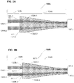
- an optical coupler array 10A which comprises a common housing structure 14A (described below), at least one VC waveguide, shown in FIG. 1A by way of example, as a single VC waveguide 30A, and at least one Non-VC waveguide, shown in FIG. 1A by way of example, as a pair of Non-VC waveguides 32A-1, 32A-2, each positioned symmetrically proximally to one of the sides of the example single VC waveguide 30A, wherein the section of the VC waveguide 30A, located between positions B and D of FIG. 1A is embedded in the common housing structure 14A.
- the VC waveguide 30A has a larger end (proximal to position B shown in FIG. 1A ), and a tapered, smaller end (proximal to position C shown in FIG. 1A ), and comprises an inner core 20A (comprising a material with an effective refractive index of N-1), an outer core 22A (comprising a material with an effective refractive index of N-2, smaller than N-1), and a cladding 24A (comprising a material with an effective refractive index of N-3, smaller than N- 2).
- the outer core 22A serves as the effective cladding at the VC waveguide 30A large end at which the VC waveguide 30A supports "M1" spatial propagating modes within the inner core 20A, where M1 is larger than 0.
- the indices of refraction N-1 and N-2, are preferably chosen so that the numerical aperture (NA) at the VC waveguide 30A large end matches the NA of an optical device (e.g.
- an optical fiber) to which it is connected such as an optical device 34A-1, for example, comprising a standard / conventional optical fiber connected to the VC waveguide 30A at a connection position 36A-1 (e.g., by a fusion splice, a mechanical connection, or by other fiber connection designs), while the dimensions of the inner and outer cores (20A, 22A), are preferably chosen so that the connected optical device (e.g., the optical device 34A-1), has substantially the same mode field dimensions (MFD).
- mode field dimensions instead of commonly used mode field diameter (also MFD) due to the case that the cross section of the VC or Non-VC waveguides may not be circular, resulting in a non-circular mode profile.
- the mode field dimensions include both the mode size and the mode shape and equal to the mode field diameter in the case of a circularly symmetrical mode.
- the coupler array 10A During fabrication of the coupler array 10A from an appropriately configured preform (comprising the VC waveguide 30A preform having the corresponding inner and outer cores 20A, 22A, and cladding 24A), as the coupler array 10A preform is tapered in accordance with at least one predetermined reduction profile, the inner core 20A becomes too small to support all M1 modes.
- the number of spatial modes, supported by the inner core at the second (tapered) end is M2, where M2 ⁇ M1.
- M1 1 (corresponding to 2 polarization modes)
- M2 0, meaning that inner core is too small to support light propagation.
- the VC waveguide 30A then acts as if comprised a fiber with a single core of an effective refractive index close to N-2, surrounded by a cladding of lower index N-3.
- a channel-to-channel spacing S-1 at the coupler array 10A larger end decreases in value to a channel-to-channel spacing S-2 at the coupler array 10A smaller end (at position C, FIG. 1A ), in proportion to a draw ratio selected for fabrication, while the MFD value (or the inversed NA value of the VC waveguide 30A) can be either reduced, increased or preserved depending on a selected differences in refractive indices, (N-1 - N-2) and (N-2 - N-3), which depends upon the desired application for the optical coupler array 10A, as described below.
- the capability of independently controlling the channel-to-channel spacing and the MFD values at each end of the optical coupler array is a highly advantageous feature of certain embodiments. Additionally, the capability to match MFD and NA values through a corresponding selection of the sizes and shapes of inner 20A and outer 22A cores and values of N-1, N-2, and N-3, makes it possible to utilize the optical coupler array to couple to various waveguides without the need to use a lens.
- the property of the VC waveguide permitting light to continue to propagate through the waveguide core along the length thereof when its diameter is significantly reduced advantageously, reduces optical loss from interfacial imperfection or contamination, and allows the use of a wide range of materials for a medium 28A of the common housing structure 14A (described below), including, but not limited to:
- the desired relative values of NA-1 and NA-2 (each at a corresponding end of the coupler array 10A, for example, NA-1 corresponding to the coupler array 10A large end, and NA-2 corresponding to the coupler array 10A small end), and, optionally, the desired value of each of NA-1 and NA-2), may be determined by selecting the values of the refractive indices N1, N2, and N3 of the coupler array 10A, and configuring them in accordance with at least one of the following relationships, selected based on the desired relative numerical aperture magnitudes at each end of the coupler array 10A : Desired NA-1/NA-2 Relative Magnitude Corresponding Relationship bet. N1, N2, N3 NA-1 (lrg.
- NA-2 (sm. end) NA-2 (sm. end)
- N1 - N2 N2 - N3
- NA-1 (lrg. end) NA-2 (sm. end)
- N1 - N2 N2 - N3)
- NA n core 2 ⁇ n clad 2 , where n core and n clad are the refractive indices of fiber core and cladding respectively.
- NA single-mode
- the various NA values are preferably determined utilizing effective indices of refraction for both n core and n cladding , because the effective indices determine the light propagation and are more meaningful in the case of structured waveguides utilized in various examples and embodiments.
- a transverse refractive index profile inside a waveguide may not be flat, but rather varying around the value N1, N2, N3, or N4.
- the transition between regions having refractive indices N1, N2, N3, and N4 may not be as sharp as a step function due to dopant diffusion or some other intentional or non-intentional factors, and may be a smooth function, connecting the values of N1, N2, N3, and N4.
- Coupling design or optimization may involve changing both the values of N1, N2, N3, and N4 and the sizes and shapes of the regions having respective indices.
- the common coupling structure 14A comprises the medium 28A, in which the section of the VC waveguide 30A located between positions B and D of FIG. 1A is embedded, and which may include, but is not limited to, at least one of the following materials:
- the VC waveguide 30A is spliced, at a particular splice location 36A-1 (shown by way of example as positioned inside the common housing structure 14A), to a corresponding respective elongated optical device 34A-1 (for example, such as an optical fiber), at least a portion of which extends outside the common housing structure 14A by a predetermined length 12A, while the Non-VC waveguides 32A-1, 32A-2 are spliced, at particular splice locations 36A-2, 36A-3, respectively (disposed outside of the common housing structure 14A), to corresponding respective elongated optical devices 34A-2, 34A-3 (such as optical fibers), and extending outside the common housing structure 14A by a predetermined length 12A.
- a particular splice location 36A-1 shown by way of example as positioned inside the common housing structure 14A
- a corresponding respective elongated optical device 34A-1 for example, such as an optical fiber
- the Non-VC waveguides 32A-1, 32A-2
- the coupler array 10A may also include a substantially uniform diameter tip 16A (shown between positions C and D in FIG. 1A ) for coupling, at an array interface 18A with the interface 42A of an optical waveguide device 40A.
- the uniform diameter tip 16A may be useful in certain interface applications, such as for example shown in FIGs. 1D , 4 and 5 .
- the coupler array 10A may be fabricated without the tip 16A (or have the tip 16A removed after fabrication), such that coupling with the optical device interface 42A, occurs at a coupler array 10A interface at position C of FIG. 1A .
- the optical device 40A comprises a double-clad fiber
- the small end of the coupler array 10A is coupled (for example, fusion spliced) to the optical device interface 42A
- at least a portion of the common housing structure 14A proximal to the splice position may be coated with a low index medium (not shown), extending over the splice position and up to the double-clad fiber optical device 40A outer cladding (and optionally extending over a portion of the double-clad fiber optical device 40A outer cladding that is proximal to the splice position).
- the coupler array 10B comprises a common housing structure 14B, at least one VC waveguide, shown in FIG. 1B by way of example, as a single VC waveguide 30B, and at least one Non-VC waveguide, shown in FIG. 1B by way of example, as a single Non-VC waveguide 32B, disposed in parallel proximity to the VC waveguide 30B, where a portion of the optical coupler array 10B, has been configured to comprise a larger channel-to-channel spacing value S2' at its small end, than the corresponding channel-to-channel spacing value S2 at the small end of the optical coupler array 10A, of FIG.
- This configuration may be readily implemented by transversely cutting the optical fiber array 10A at a position C', thus producing the common housing structure 14B that is shorter than the common housing structure 14A and resulting in a new, larger diameter array interface 18B, having the larger channel-to-channel spacing value S2'.
- the coupler array 10C comprises a plurality of VC waveguides, shown in FIG. 1C as VC waveguides 30C-1, and 30C-2, and a plurality of Non-VC waveguides, shown in FIG.
- Non-VC waveguides 32C-1, 32C-2, and 32C-a all disposed longitudinally and asymmetrically to one another, wherein at least a portion of the plural Non-VC waveguides are of different types and/or different characteristics (such as single mode or multimode or polarization maintaining etc.) - for example, Non-VC waveguides 32C-1, 32C-2 are of a different type, or comprise different characteristics from the Non-VC waveguide 32C-a.
- any of the VC or Non-VC waveguides can readily extend beyond the coupler array 10C common housing structure by any desired length, and need to be spliced to an optical device proximally thereto.
- the coupler array 50 comprises a pair of optical fiber coupler array components (10D-1 and 10D-2), with a multi-core optical fiber element 52 connected (e.g., by fusion splicing at positions 54-1 and 54-2) between the second (smaller sized) ends of the two optical fiber coupler array components (10D-1, 10D-2).
- At least one of the VC waveguides in each of the coupler array components (10D-1, 10D-2) is configured to increase or maximize optical coupling to a corresponding selected core of the multi-core optical fiber element 52, while decreasing or minimizing optical coupling to all other cores thereof.
- the coupler array 100A comprises a plurality of longitudinally proximal VC waveguides at least partially embedded in a single common housing structure 104A, shown by way of example only, as plural VC waveguides 130A-1, 130A-2.
- Each plural VC waveguide 130A-1, 130A-2 is spliced, at a particular splice location 132A-1, 132A-2, respectively, to a corresponding respective elongated optical device 134A-1, 134A-2 (such as an optical fiber), at least a portion of which extends outside the common housing structure 104A by a predetermined length 102A, and wherein each particular splice location 132A-1, 132A-2 is disposed within the common housing structure 104A.
- FIG. 2B a sixth example of the optical fiber coupler array, is shown as a coupler array 100B.
- the coupler array 100B comprises a plurality of longitudinally proximal VC waveguides at least partially embedded in a single common housing structure 104B, shown by way of example only, as plural VC waveguides 130B-1, 130B-2.
- Each plural VC waveguide 130B-1, 130B-2 is spliced, at a particular splice location 132B-1, 132B-2, respectively, to a corresponding respective elongated optical device 134B-1, 134B-2 (such as an optical fiber), at least a portion of which extends outside the common housing structure 104B by a predetermined length 102B, and wherein each particular splice location 132B-1, 132B-2 is disposed at an outer cross-sectional boundary region of the common housing structure 104B.
- a seventh example of the optical fiber coupler array is shown as a coupler array 100C.
- the coupler array 100C comprises a plurality of longitudinally proximal VC waveguides at least partially embedded in a single common housing structure 104C, shown by way of example only, as plural VC waveguides 130C-1, 130C-2.
- Each plural VC waveguide 130C-1, 130C-2 is spliced, at a particular splice location 132C-1, 132C-2, respectively, to a corresponding respective elongated optical device 134C-1, 134C-2 (such as an optical fiber), at least a portion of which extends outside the common housing structure 104C by a predetermined length 102C, and wherein each particular splice location 132C-1, 132C-2 is disposed outside of the common housing structure 104C.
- the coupler array 150 comprises a plurality of longitudinally proximal VC waveguides at least partially embedded in a single common housing structure, that is configured at its second end, to increase or optimize optical coupling to a free-space-based optical device 152.
- the free-space-based optical device 152 may comprise a lens 154 followed by an additional optical device component 156, which may comprise, by way of example, a MEMS mirror or volume Bragg grating.
- the combination of the coupler and the free-space-based optical device 152 may be used as an optical switch or WDM device for spectral combining or splitting of light signals 160b (representative of the light coupler array 150 output light signals 160a after they have passed through the lens 154.)
- one of the fibers may be used as an input and all others for an output or vice versa.
- single or individual coupler array components/elements are identified by a single reference number, while each plurality of the coupler component/elements is identified by a reference number followed by a "(1..n)" designation, with "n” being a desired number of plural coupler elements/components (and which may have a different value in any particular coupler array example described below).
- all the waveguides VC and Non-VC are shown with a circular cross-section of the inner and outer core and cladding only by example.
- Other shapes of the cross-sections of the inner and outer core and cladding may be utilized without departure from the current invention.
- the specific choice of shape is based on various requirements, such as channel shape of the optical device, channel positional geometry (for example, hexagonal, rectangular or square lattice), or axial polarization alignment mode.
- the sizes, relative sizes, relative positions and choices of composition materials are not limited to the example sizes, relative sizes, relative positions and choices of composition materials, indicated below in connection with the detailed descriptions of the coupler array examples of FIGs. 3A to 3L , but rather they may be selected by one skilled in the art as a matter of convenience or design choice.
- each of the various single common housing structure components 202A to 202L, of the various coupler arrays 200A to 200L of FIGs. 3A to 3L may be composed of a medium having the refractive index N-4 value in accordance with an applicable one of the above-described relationships with the values of other coupler array component refractive indices N-1, N-2, and N-3, and having properties and characteristics selected from the various contemplated example medium composition parameters described above in connection with medium 28A of FIG. 1A .
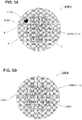
- FIG. 3A a first alternative of the optical fiber coupler arrays of FIGs. 1D to 2D , is shown as a coupler array 200A in which all waveguides are VC waveguides.
- the coupler array 200A comprises a single common housing 202A, and plurality of VC waveguides 204A-(1..n), with n being equal to 19 by way of example only, disposed centrally along the central longitudinal axis of the housing 202A.
- the coupler array 200A may also comprise an optional at least one fiducial element 210A, operable to provide one or more useful properties to the coupler array, including, but not limited to:
- a fiducial element when deployed in optical coupler arrays that comprise at least one polarization maintaining VC waveguide (such as the optical coupler arrays described below in connection with FIGs. 3H - 3L ), is further operable to:
- the fiducial element 210A may comprise any of the various types of fiducial elements known in the art, for example, it may be a dedicated elongated element positioned longitudinally within the common housing structure 202A in one of various cross-sectional positions (such as positions X or Y, shown in FIG. 3A .
- the fiducial element 210A may comprise a dedicated channel not used for non-fiducial purposes, for example, replacing one of the waveguides 204A-(1..n), shown by way of example only at position Z in FIG. 3A .
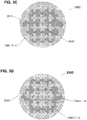
- a first alternative of the optical fiber coupler array 10A of FIG. 1A is shown as a coupler array 200B, that comprises a single housing structure 202B, and at least one VC waveguide, shown in FIG. 3B by way of example as a VC waveguide 204B, and a plurality of Non-VC waveguides 206B-(1..n), with n being equal to 18 by way of example only.
- the VC waveguide 204B is positioned along a central longitudinal axis of the common housing structure 202B, and circumferentially and symmetrically surrounded by proximal parallel plural Non-VC waveguides 206B- (1..n).
- a first alternative of the optical fiber coupler array 200B of FIG. 3B is shown as a coupler array 200C that comprises a single housing structure 202C, a VC waveguide 204C, and a plurality of Non-VC waveguides 206C-(1..n), with n being equal to 18 by way of example only.
- the VC waveguide 204C is positioned along a central longitudinal axis of the common housing structure 202C, and circumferentially and symmetrically surrounded by proximal parallel plural Non-VC waveguides 206C-(1..n).
- the coupler array 200C is configured such that a volume of the common housing structure 202C medium, surrounding the sections of all of the waveguides embedded therein (i.e., the VC waveguide 204C and the plural Non-VC waveguides 206C-(1..n)), exceeds a total volume of the inner and outer cores of the section of the VC waveguide 204C that is embedded within the single common housing structure 202C.
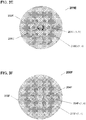
- a first alternative of the optical fiber coupler array 200C of FIG. 3C is shown as a coupler array 200D that comprises a single housing structure 202D, a plurality of VC waveguides 204D-(1..N), with N being equal to 7 by way of example only, and a plurality of Non-VC waveguides 206D-(1..n), with n being equal to 12 by way of example only.
- the plural VC waveguides 204D-(1..N) are positioned along a central longitudinal axis of the common housing structure 202D, and circumferentially and symmetrically surrounded by proximal parallel plural Non- VC waveguides 206D-(1..n).
- the coupler array 200D is configured such that a volume of the common housing structure 202D medium, surrounding the sections of all of the waveguides embedded therein (e.g., the plural VC waveguides 204D-(1..N), and the plural Non-VC waveguides 206D-(1..n)), exceeds a total volume of the inner and outer cores of the section of the plural VC waveguides 204D-(1..N) that are embedded within the single common housing structure 202D.
- a first alternative of the optical fiber coupler array 200D of FIG. 3D is shown as a coupler array 200E, that comprises a single housing structure 202E, a plurality of VC waveguides 204E-(1..N), with N being equal to 6 by way of example only, a plurality of Non-VC waveguides 206E-(1..n), with n being equal to 12 by way of example only, and a separate single Non-VC waveguide 206E'.
- the Non-VC waveguide 206E' is preferably operable to provide optical pumping functionality therethrough, and is positioned along a central longitudinal axis of the common housing structure 202E and circumferentially and symmetrically surrounded by proximal parallel plural VC waveguides 204E-(1..N), that are in turn circumferentially and symmetrically surrounded by proximal parallel plural Non- VC waveguides 206E-(1..n).
- a second alternative of the optical fiber coupler array 200B of FIG. 3B is shown as a coupler array 200F, that comprises a single housing structure 202F, a plurality of VC waveguides 204F-(1..N), with N being equal to 6 by way of example only, a separate single VC waveguide 204F', and a plurality of Non-VC waveguides 206F-(1..n), with n being equl to 12 by way of example only, that preferably each comprise enlarged inner cores of sufficient diameter to increase or optimize optical coupling to different types of optical pump channels of various optical devices, to which the coupler array 200F may be advantageously coupled.
- the VC waveguide 204F' is positioned along a central longitudinal axis of the common housing structure 202F, and circumferentially and symmetrically surrounded by proximal parallel plural VC waveguides 204F-(1..N), that are in turn circumferentially and symmetrically surrounded by proximal parallel plural Non- VC waveguides 206F-(1..n).
- FIG. 3G a third alternative of the optical fiber coupler array 200B of FIG. 3B , above, is shown as a coupler array 200G, that comprises a single housing structure 202G, and at least one VC waveguide, shown in FIG. 3G by way of example as a VC waveguide 204G, and a plurality of Non-VC waveguides 206G-(1..n), with n being equal to 18 by way of example only.
- the VC waveguide 204G is positioned as a side-channel, off-set from the central longitudinal axis of the single common housing structure 202G, such that optical fiber coupler array 200G may be readily used as a fiber optical amplifier and or a laser, when spliced to a double-clad optical fiber (not shown) having a non-concentric core for improved optical pumping efficiency.
- a double-clad fiber is a fiber in which both the core and the inner cladding have light guiding properties
- most optical fiber types such as SM, MM, LMA, or MC (multi-core), whether polarization maintaining or not, and even standard (e.g., conventional) single mode optical fibers, can be converted into a double-clad fiber by coating (or recoating) the fiber with a low index medium (forming the outer cladding).
- the second end of the coupler array 200G when the second end of the coupler array 200G is spliced to a double-clad fiber (not shown), at least a portion of the common housing structure 202G proximal to the splice point with the double-clad fiber (not-shown), may be coated with a low index medium extending over the splice point and up to the double-clad fiber's outer cladding (and optionally extending over a portion of the outer cladding that is proximal to the splice point).
- At least one of the VC waveguides utilized therein, and, in certain embodiments, optionally at least one of the Non-VC waveguides may comprise a polarization maintaining (PM) property.
- the PM property of a VC waveguide may result from a pair of longitudinal stress rods disposed within the VC waveguide outside of its inner core and either inside, or outside, of the outer core (or through other stress elements), or the PM property may result from a noncircular inner or outer core shape, or from other PM-inducing optical fiber configurations (such as in bow-tie or elliptically clad PM fibers).
- an axial alignment of the PM waveguides (or waveguide), in accordance with a particular polarization axes alignment mode may be involved.
- a polarization axes alignment mode may comprise, but is not limited to, at least one of the following:
- the selection of a specific type of polarization axes alignment mode for the various examples of the optical coupler is preferably governed by at least one axes alignment criterion, which may include, but which is not limited to: alignment of PM waveguides' polarization axes in a geometric arrangement that increases or maximizes PM properties thereof; and/or satisfying at least one requirement of one or more intended industrial application for the coupler array.
- FIG. 3H a first alternative of the optical fiber coupler array 200G of FIG. 3G , above, is shown as a coupler array 200H, that comprises a single housing structure 202H, and at least one VC waveguide, shown in FIG. 3H by way of example as a PM VC waveguide 204H having polarization maintaining properties, and a plurality of Non-VC waveguides 206H-(1..n), with n being equal to 18 by way of example only.
- the PM VC waveguide 204H is positioned as a side-channel, off-set from the central longitudinal axis of the single common housing structure 202H, and comprises a polarization axis that is aligned, by way of example, with respect to the transverse off-center location of the PM VC waveguide 204H.
- FIG. 3I a fourth alternative of the optical fiber coupler array 200B of FIG. 3B , above, is shown as a coupler array 2001, that comprises a single housing structure 2021, and at least one VC waveguide, shown in FIG. 3I by way of example as a PM VC waveguide 2041 having polarization maintaining properties, and a plurality of PM Non-VC waveguides 206I-(1..n), with n being equal to 18 by way of example only, each also having polarization maintaining properties.
- the PM VC waveguide 204I is positioned along a central longitudinal axis of the common housing structure 202I, and circumferentially and symmetrically surrounded by proximal parallel plural PM Non-VC waveguides 206I-(1..n).
- the coupler array 200I comprises a polarization axes alignment mode in which the polarization axes of each of the PM VC waveguide 204I and of the plural PM Non-VC waveguides 2061-(1..n) are aligned to one another.
- the PM properties of the PM VC waveguide 204I and of the plural PM Non-VC waveguides 206I-(1..n) are shown, by way of example only, as being induced by rod stress members (and which may readily and alternately be induced by various other stress, or equivalent designs)).
- FIG. 3J a first alternative of the optical fiber coupler array 200I of FIG. 3I , above, is shown as a coupler array 200J, that comprises a single housing structure 202J, and at least one VC waveguide, shown in FIG. 3J by way of example as a PM VC waveguide 204J having polarization maintaining properties, and a plurality of PM Non-VC waveguides 206J-(1..n), with n being equal to 18 by way of example only, each also having polarization maintaining properties.
- the PM VC waveguide 204J is positioned along a central longitudinal axis of the common housing structure 202J, and circumferentially and symmetrically surrounded by proximal parallel plural PM Non-VC waveguides 206J-(1..n).
- the PM properties of the PM VC waveguide 204J and of the plural PM Non-VC waveguides 206J-(1..n) are shown, by way of example only, as resulting only from a non-circular cross-sectional shape (shown by way of example only as being at least in part elliptical), of each plural PM Non-VC waveguide 206J-(1..n) core (and from a non-circular cross-sectional shape of the outer core of the PM VC waveguide 204J).
- the coupler array 200J optionally comprises at least one waveguide arrangement indication element 208J, positioned on an outer region of the common housing structure 202J, that is representative of the particular cross-sectional geometric arrangement of the optical coupler array 200J waveguides (i.e., of the PM VC waveguide 204J and of the plural PM Non-VC waveguides 206J-(1..n)), such that a particular cross-sectional geometric waveguide arrangement may be readily identified from at least one of a visual and physical inspection of the common coupler housing structure 202J that is sufficient to examine the waveguide arrangement indication element 208J.
- the waveguide arrangement indication element 208J may be configured to be further operable to facilitate passive alignment of a second end of the optical coupler array 200J to at least one optical device (not shown).
- the waveguide arrangement indication element 208J may comprise, but is not limited to, one or more of the following, applied to the common housing structure 202J outer surface: a color marking, and/or a physical indicia (such as an groove or other modification of the common housing structure 202J outer surface, or an element or other member positioned thereon).
- the waveguide arrangement indication element 208J may actually comprise a specific modification to, or definition of, the cross-sectional geometric shape of the common housing structure 202J (for example, such as a hexagonal shape of a common housing structure 202L of FIG. 3L , below, or another geometric shape).
- the coupler array 200J may comprise a polarization axes alignment mode in which the polarization axes of each of the PM VC waveguide 204J and of the plural PM Non-VC waveguides 206J-(1..n) are aligned to one another, or to the waveguide arrangement indication element 208J.
- a fifth alternative of the optical fiber coupler array 200B of FIG. 3B is shown as a coupler array 200K, that comprises a single housing structure 202K, and at least one VC waveguide, shown in FIG. 3K by way of example as a PM VC waveguide 204K having polarization maintaining properties, and a plurality of Non-VC waveguides 206K-(1..n), with n being equal to 18 by way of example only.
- the PM VC waveguide 204K is positioned along a central longitudinal axis of the common housing structure 202K, and circumferentially and symmetrically surrounded by proximal parallel plural PM Non-VC waveguides 206K-(1..n).
- the PM properties of the PM VC waveguide 204K are shown, by way of example only, as being induced by rod stress members (and which may readily and alternately be induced by various other stress, or equivalent approaches)).
- the coupler array 200K may optionally comprise a plurality of waveguide arrangement indication elementsshown by way of example only, as waveguide arrangement indication elements 208K-a and 208K-b, which may each be of the same, or of a different type, as described above, in connection with the waveguide arrangement indication element 208J of FIG. 3J .
- a second alternative of the optical fiber coupler array 200I of FIG. 3I is shown as a coupler array 200L, that comprises a single housing structure 202L comprising a cross section having a non-circular geometric shape (shown by way of example as a hexagon), and at least one VC waveguide, shown in FIG. 3L by way of example as a PM VC waveguide 204L having polarization maintaining properties, and a plurality of PM Non-VC waveguides 206L-(1..n), with n being equal to 18 by way of example only, each also having polarization maintaining properties.
- the PM VC waveguide 204L is positioned along a central longitudinal axis of the common housing structure 202L, and circumferentially and symmetrically surrounded by proximal parallel plural PM Non-VC waveguides 206L-(1..n).
- the coupler array 200L comprises a polarization axes alignment mode in which the polarization axes of each of the PM VC waveguide 204L and of the plural PM Non-VC waveguides 206L-(1..n) are aligned to one another, and to the common housing structure 202L cross-sectional geometric shape.
- the PM properties of the PM VC waveguide 204L and of the plural PM Non-VC waveguides 206L-(1..n) are shown, by way of example only, as being induced by rod stress members (and which may readily and alternately be induced by various other stress, or equivalent designs)).
- the coupler array 200K may optionally comprise a waveguide arrangement indication element 208L-a which may comprise any of the configurations described above, in connection with the waveguide arrangement indication element 208J of FIG. 3J .
- a second end 302 i.e. "tip" of the optical fiber coupler array is shown, by way of example, as being in the process of connecting to plural vertical coupling elements 306 of an optical device 304 in a proximal open air optical coupling alignment configuration, that may be readily shifted into a butt-coupled configuration through full physical contact of the optical fiber coupler array second end 302 and the vertical coupling elements 306.
- a second end 322 (i.e. "tip") of the optical fiber coupler array is shown, by way of example, as being in the process of connecting to plural edge coupling elements 326 of an optical device 324 in a butt-coupled configuration, that may be readily shifted into one of several alternative coupling configuration, including a proximal open air optical coupling alignment configuration, and or an angled alignment coupling configuration.
- the optical coupler array (i.e., such as optical coupler arrays 200D to 200L of FIGS. 3C to 3L ) may be readily configured to pump optical fiber lasers, and/or optical fiber amplifiers (or equivalent devices).
- a pumping-enabled coupler array comprises a central channel (i.e., waveguide), configured to transmit a signal (i.e., serving as a "signal channel") which will thereafter be amplified or utilized to generate lasing, and further comprises at least one additional channel (i.e., waveguide), configured to provide optical pumping functionality (i.e., each serving as a "pump channel").
- the pumping-enabled coupler array may comprise the following in any desired combination thereof:
- the pumping-enabled coupler array may be configured to selectively utilize less than all the available pumping channels. It should also be noted that, as a matter of design choice, the pumping-enabled coupler array may be configured to comprise:
- the pump channels could be positioned in any transverse position within the coupler, including along the central longitudinal axis.
- the pump channels may also comprise, but are not limited to, at least one of any of the following optical fiber types: SM, MM, LMA, or VC waveguides.
- any of the optical fiber(s) being utilized as an optical pump channel (regardless of the fiber type) in the coupler may comprise polarization maintaining properties.
- the pumping-enabled coupler array may be configured to be optimized for coupling to a double-clad fiber - in this case, the signal channel of the coupler array would be configured or optimized for coupling to the signal channel of the double-clad fiber, while each of the at least one pumping channels would be configured or optimized to couple to the inner cladding of the double-clad fiber.
- optical coupler arrays may also be readily implemented as high density, multi-chanel, optical input/output (I/O) for fiber-to-chip and fiber-to-optical waveguides.
- the optical fiber couplers may readily comprise at least the following features:
- optical fiber couplers may be advantageously utilized for at least the following applications.
- the various examples of the optical fiber couplers comprise at least the following advantages, as compared to currently available competitive solutions:
- FIG. 7 at least one embodiment of a flexible optical fiber coupler array according to the invention is shown as a flexible pitch reducing optical fiber array (PROFA) coupler 450.
- PROFA flexible pitch reducing optical fiber array
- the flexible PROFA coupler 450 shown in FIG. 7 can be configured for use in applications where interconnections with low crosstalk and sufficient flexibility to accommodate low profile packaging are desired.
- the vanishing core approach described herein and in U.S. Patent Application Publication No. 2013/0216184 , entitled “CONFIGURABLE PITCH REDUCING OPTICAL FIBER ARRAY", allows for the creation of a pitch reducing optical fiber array (PROFA) coupler / interconnect operable to optically couple, for example, a plurality of optical fibers to an optical device (e.g., a PIC), which can be butt-coupled to an array of vertical grating couplers (VGCs).
- VCCs vertical grating couplers
- the vanishing core approach can be utilized once more to reduce the outside diameter further without substantially compromising the channel crosstalk. This further reduction can advantageously provide certain embodiments with a flexible region which has a reduced cross section between a first and second end.
- the difference (N-2A minus N-3) is larger than the differences (N-2 minus N-2A) or (N-1 minus N-2), resulting in a high NA, bend insensitive waveguide, when the light is guided by the additional layer having refractive index N-2A.
- the outer diameter can then be expanded along the longitudinal length toward the second end, resulting in a lower NA waveguide with larger coupling surface area at the second end.
- an optical coupler array 450 comprise an elongated optical element 1000 having a first end 1010, a second end 1020, and a flexible portion 1050 therebetween.
- the optical element 1000 includes a coupler housing structure 1060 and a plurality of longitudinal waveguides 1100 embedded in the housing structure 1060.
- the waveguides 1100 are arranged with respect to one another in a cross-sectional geometric waveguide arrangement.
- FIG. 7 the example cross-sectional geometric waveguide arrangements of the waveguides 1100 for the first end 1010, the second end 1020, and at a location within the flexible portion 1050 are shown.
- the cross-sectional geometric waveguide arrangement of the waveguides 1100 for an intermediate location 1040 between the first end 1010 and the flexible portion 1050 is also shown. As illustrated by the shaded regions within the cross sections and as will be described herein, light can be guided through the optical element 1000 from the first end 1010 to the second end 1020 through the flexible portion 1050. As also shown in FIG. 7 , the result is a structure, which maintains all channels discretely with sufficiently low crosstalk, while providing enough flexibility (e.g., with the flexible portion 1050) to accommodate low profile packaging.
- a low crosstalk can be considered within a range from -45 dB to -35 dB, while in other embodiments, a low crosstalk can be considered within a range from -15 dB to -5 dB. Accordingly, the level of crosstalk is not particularly limited.
- the crosstalk can be less than or equal to -55 dB, -50 dB, -45 dB, -40 dB, -35 dB, -30 dB, -25 dB, -20 dB, -15 dB, -10 dB, 0 dB, or any values therebetween (e.g., less than or equal to -37 dB, -27 dB, -17 dB, -5 dB, etc.)
- the crosstalk can be within a range from -50 dB to -40 dB, from -40 dB to -30 dB, from -30 dB to -20 dB, from -20 dB to -10 dB, from -10 dB to 0 dB, from -45 dB to -35 dB, from -35 dB to -25 dB, from -25 dB to -15 dB, from -15 d
- the flexibility can also depend on the application of the array.
- good flexibility of the flexible portion 1050 can comprise bending of at least 90 degrees, while in other embodiments, a bending of at least 50 degrees may be acceptable. Accordingly, the flexibility is not particularly limited. In some embodiments, the flexibility can be at least 45 degrees, 50 degrees, 55 degrees, 60 degrees, 65 degrees, 70 degrees, 75 degrees, 80 degrees, 90 degrees, 100 degrees, 110 degrees, 120 degrees, or at least any value therebetween.
- the flexible portion 1050 can bend in a range formed by any of these values, e.g., from 45 to 55 degrees, from 50 to 60 degrees, from 60 to 70 degrees, from 70 to 80 degrees, from 80 to 90 degrees, from 90 to 100 degrees, from 100 to 110 degrees, from 110 to 120 degrees, or any combinations of these ranges, or any ranges formed by any values within these ranges (e.g., from 50 to 65 degrees, from 50 to 85 degrees, from 65 to 90 degrees, etc.) In other embodiments, the flexible portion 1050 can bend more or less than these values. Bending can typically be associated with light scattering. However, various embodiments can be configured to bend as described herein (e.g., in one of the ranges described above) and achieve relatively low crosstalk as described herein (e.g., in one of the ranges described above).
- the flexible portion 1050 might not bend in use, however the flexibility can be desired for decoupling the first 1010 or second 1020 end from other parts of the coupler array 450.
- the flexible portion 1050 of the flexible PROFA coupler 450 can provide mechanical isolation of the first end 1010 (e.g., a PROFA-PIC interface) from the rest of the PROFA, which results in increased stability with respect to environmental fluctuations, including temperature variations and mechanical shock and vibration.
- the coupler array 450 is configured to optically couple with a plurality of optical fibers 2000 and/or with an optical device 3000.
- the optical fibers 2000 and optical device 3000 can include any of those described herein.
- the coupler array 450 can couple with the optical fibers 2000 via the plurality of waveguides 1100 at the first end 1010.
- the coupler array 450 can couple with the optical device 3000 via the plurality of waveguides 1100 at the second end 1020.
- the plurality of waveguides 1100 comprises at least one VC waveguide 1101.
- FIG. 7 illustrates all of the waveguides 1100 as VC waveguides. However, one or more Non-VC waveguides may also be used.
- FIG. 7 illustrates 7 VC waveguides, yet any number of VC and/or Non-VC waveguides can be used.
- each of the waveguides 1100 is disposed at an individual corresponding cross-sectional geometric position, relative to other waveguides of the plurality of waveguides 1100.
- FIG. 7 shows a waveguide surrounded by 6 other waveguides
- the cross-sectional geometric waveguide arrangement is not limited and can include any arrangement known in the art or yet to be developed including any of those shown in FIGs. 3A-3L .
- the VC waveguide 1101 comprises an inner core (e.g., an inner vanishing core) 1110, an outer core 1120, and an outer cladding 1130 with refractive indices N-1, N-2, and N-3 respectively.
- the VC waveguide 1101 further comprises a secondary outer core 1122 (e.g., between the outer core 1120 and the outer cladding 1130) having refractive index N-2A.
- the outer core 1120 longitudinally surrounds the inner core 1110
- the secondary outer core 1122 longitudinally surrounds the outer core 1120 with the outer cladding 1130 longitudinally surrounding the secondary outer core 1122.
- the relationship between the refractive indices of the inner core 1110, outer core 1120, secondary outer core 1122, and outer cladding 1130 is advantageously N-1 > N-2 > N2-A > N-3.
- each surrounding layer serves as an effective cladding to the layers within it (e.g., the outer core 1120 can serve as an effective cladding to the inner core 1110, and the secondary outer core 1122 can serve as an effective cladding to the outer core 1120).
- the use of the secondary outer core 1122 can provide an additional set of core and cladding.
- the secondary outer core 1122 By including the secondary outer core 1122 with a refractive index N-2A, a higher NA is achieved (e.g., compared to without the secondary outer core 1122).
- the difference (N-2A minus N-3) can be larger than the differences (N-2 minus N-2A) or (N-1 minus N-2) to result in a relatively high NA.
- Increasing NA can reduce the MFD, allowing for the channels (e.g., waveguides 1100) to be closer to each other (e.g., closer spacing between the waveguides 1100) without compromising crosstalk.
- the coupler array 450 is reduced further in cross section (e.g., compared to without the secondary outer core 1122) providing a reduced region when light is guided by the secondary outer core 1122.
- the optical fiber coupler array includes a flexible portion 1050 which is more flexible than the regions proximal to the first end 1010 and the second end 1020.
- the inner core 1110 size, the outer core 1120 size, and the spacing between the waveguides 1100 reduce (e.g., simultaneously and gradually in some instances) along the optical element 1000 from the first end 1010 to the intermediate location 1040 such that at the intermediate location 1040, the inner core 1110 size is insufficient to guide light therethrough and the outer core 1120 size is sufficient to guide at least one optical mode.
- Each waveguide 1100 has a capacity for at least one optical mode (e.g., single mode or multi-mode).
- the VC waveguide 1101 can support a number of spatial modes (M1) within the inner core 1110.
- the inner core 1110 may no longer be able to support all the M1 modes (e.g., cannot support light propagation).
- the outer core 1120 can be able to support all the M1 modes (and in some cases, able to support additional modes).
- light traveling within the inner core 1110 from the first end 1010 to the intermediate location 1040 can escape from the inner core 1110 into the outer core 1120 such that light can propagate within both the inner core 1110 and outer core 1120.
- the outer core 1120 size, the secondary outer core 1122 size, and the spacing between the waveguides 1100 reduce (e.g., simultaneously and gradually in some instances) along said optical element 1000, for example, from the intermediate location 1040 to the flexible portion 1050 such that at the flexible portion 1050, the outer core 1120 size is insufficient to guide light therethrough and the secondary outer core 1122 size is sufficient to guide at least one optical mode therethrough.
- the VC waveguide 1101 can support all the M1 modes within the outer core 1120.
- the outer core 1120 may be no longer able to support all the M1 modes (e.g., cannot support light propagation).
- the secondary outer core 1122 can be able to support all the M1 modes (and in some cases, able to support additional modes).
- light traveling within the outer core 1120 from the intermediate location 1040 to the flexible portion 1050 can escape from the outer core 1120 into the secondary outer core 1122 such that light can propagate within the inner core 1110, the outer core 1120, and secondary outer core 1122.
- the outer core 1120 size, the secondary outer core 1122 size, and the spacing between the waveguides 1100 can expand (e.g., simultaneously and gradually in some instances) along the optical element 1000 from the flexible portion 1050 to the second end 1020 such that at the second end 1020, the secondary outer core 1122 size is insufficient to guide light therethrough and the outer core 1120 size is sufficient to guide at least one optical mode therethrough.
- the secondary outer core 1122 may no longer be able to support all the M1 modes (e.g., cannot support light propagation).
- the outer core 1120 can be able to support all the M1 modes (and in some cases, able to support additional modes).
- light traveling within the secondary outer core 1122 from the flexible portion 1050 to the second end 1020 can return and propagate only within the inner core 1110 and the outer core 1120.
- the outer core 1120 size, the secondary outer core 1122 size, and spacing between the waveguides 1100 reduce (e.g., simultaneously and gradually in some instances) along the optical element 1000 from the second end 1020 to the flexible portion 1050 such that at the flexible portion 1050, the outer core 1120 size is insufficient to guide light therethrough and the secondary outer core 1122 size is sufficient to guide at least one optical mode therethrough.
- the reduction in cross-sectional core and cladding sizes can advantageously provide rigidity and flexibility in a coupler array 450. Since optical fibers 2000 and/or an optical device 3000 can be fused to the ends 1010, 1020 of the coupler array 450, rigidity at the first 1010 and second 1020 ends can be desirable. However, it can also be desirable for coupler arrays to be flexible so that they can bend to connect with low profile integrated circuits.
- the flexible portion 1050 between the first 1010 and second 1020 ends can allow the first 1010 and second 1020 ends to be relatively rigid, while providing the flexible portion 1050 therebetween.
- the flexible portion can extend over a length of the optical element 1000 and can mechanically isolate the first 1010 and second 1020 ends.
- the flexible portion 1050 can mechanically isolate the first end 1010 from a region between the flexible portion 1050 and the second end 1020.
- the flexible portion 1050 can mechanically isolate the second end 1020 from a region between the first end 1010 and the flexible portion 1050.
- Such mechanical isolation can provide stability to the first 1010 and second 1020 ends, e.g., with respect to environmental fluctuations, including temperature variations and mechanical shock and vibration.
- the length of the flexible portion 1050 is not particularly limited and can depend on the application.
- the length can be in a range from 2 to 7 mm, from 3 to 8 mm, from 5 to 10 mm, from 7 to 12 mm, from 8 to 15 mm, any combination of these ranges, or any range formed from any values from 2 to 20 mm (e.g., 3 to 13 mm, 4 to 14 mm, 5 to 17 mm, etc.).
- the length of the flexible portion 1050 can be shorter or longer.
- the flexible portion 1050 can provide flexibility.
- the flexible portion 1050 can have a substantially similar cross-sectional size (e.g., the cross-sectional size of the waveguides 1100) extending over the length of the flexible portion 1050.
- the cross-section size at the flexible portion 1050 can comprise a smaller cross-sectional size than the cross-sectional size at the first 1010 and second 1020 ends. Having a smaller cross-sectional size, this flexible portion 1050 can be more flexible than a region proximal to the first 1010 and second 1020 ends.
- the smaller cross-sectional size can result from the reduction in core and cladding sizes.
- An optional etching post-process may be desirable to further reduce the diameter of the flexible length of the flexible PROFA coupler 450.
- the flexible portion 1050 can be more flexible than a standard SMF 28 fiber. In some examples, the flexible portion 1050 can bend at least 45 degrees, 50 degrees, 55 degrees, 60 degrees, 65 degrees, 70 degrees, 75 degrees, 80 degrees, 90 degrees, 100 degrees, 110 degrees, 120 degrees, or at least any value therebetween.
- the flexible portion 1050 can bend in a range formed by any of these values, e.g., from 45 to 55 degrees, from 50 to 60 degrees, from 60 to 70 degrees, from 70 to 80 degrees, from 80 to 90 degrees, from 90 to 100 degrees, from 100 to 110 degrees, from 110 to 120 degrees, or any combinations of these ranges, or any ranges formed by any values within these ranges (e.g., from 50 to 65 degrees, from 50 to 85 degrees, from 65 to 90 degrees, etc.) In other examples, the flexible portion 1050 can bend more or less than these values. As described herein, in various applications, the flexible portion 1050 might not bend in use, however the flexibility can be desired for decoupling the first 1010 or second 1020 end from other parts of the coupler array 450.
- the coupler array 450 comprises a coupler housing structure 1060.
- the coupler housing structure 1060 can include a common single coupler housing structure.
- the coupler housing structure 1060 comprises a medium 1140 (e.g., having a refractive index N-4) surrounding the waveguides 1100.
- N-4 is greater than or equal to N-3.
- the medium 1140 can include any medium as described herein (e.g., pure-silica).
- the medium can also include glass such that the coupler array 450 can be an all-glass coupler array.
- the waveguides 1100 can be embedded within the medium 1040 of the housing structure 1060.
- a total volume of the medium 1140 of the coupler housing structure 1060 can be greater than a total volume of all the inner and outer cores 1110, 1120, 1122 of the VC waveguides confined within the coupler housing structure 1060.
- Each waveguide can couple to the optical fibers 2000 and/or optical device 3000 at a location inside, outside, or at a boundary region of the coupler housing structure 1060, e.g., as shown in FIGs. 1A to 2D .
- the first end 1010 and the second end 1020 can each be configured for the optical fibers 2000 or optical device 3000 with which it is coupled.
- the MFD of the VC waveguide at the first 1010 and/or second 1020 ends can be configured (e.g., using the sizes of the cores) to match or substantially match the MFD of the optical fiber 2000 or optical device 3000 with which it is coupled.
- the NA of the VC waveguide at the first 1010 and/or second 1020 ends can be configured (e.g., using the refractive indices) to match or substantially match the NA of the optical fiber 2000 or optical device 3000 with which it is coupled.
- the refractive indices can be modified in any way known in the art (e.g., doping the waveguide glass) or yet to be developed.
- the difference (N-1 minus N-2) can be greater than the difference (N-2 minus N-2A) such that the NA at the first end 1010 is greater than the NA at the second end 1020.
- the difference (N-1 minus N-2) can be less than the difference (N-2 minus N-2A) such that the NA at the first end 1010 is less than the NA at the second end 1020.
- the difference (N-1 minus N-2) can be equal to (N-2 minus N-2A) such that the NA at the first end 1010 is equal to the NA at the second end 1020.
- the VC waveguide can include any of the fiber types described herein including but not limited to a single mode fiber, a multi-mode fiber, and/or a polarization maintaining fiber.
- the core and cladding (1110, 1120, 1122, 1130) sizes are not particularly limited.
- the inner 1110 and/or outer 1120 core sizes can be in a range from 1 to 3 microns, from 2 to 5 microns, from 4 to 8 microns, from 5 to 10 microns, any combination of these ranges, or any range formed from any values from 1 to 10 microns (e.g., 2 to 8 microns, 3 to 9 microns, etc.). However, the sizes can be greater or less.
- the inner 1110 and/or outer 1120 core sizes can range from submicrons to many microns, to tens of microns, to hundreds of microns depending, for example, on the wavelength and/or number of modes desired.
- the difference in the refractive indices is not particularly limited.
- the index difference can be in a range from 1.5 x 10 -3 to 2.5 x 10 -3 , from 1.7 x 10 -3 to 2.3 x 10 -3 , from 1.8 x 10 -3 to 2.2 x 10 -3 , from 1.9 x 10 -3 to 2.1 x 10 -3 , from 1.5 x 10 -3 to 1.7 x 10 -3 , from 1.7 x 10 -3 to 1.9 x 10 -3 , from 1.9 x 10 -3 to 2.1 x 10 -3 , from 2.1 x 10 -3 to 2.3 x 10 -3 , from 2.3 x 10 -3 to 2.5 x 10 -3 , any combination of these ranges, or any range formed from any values from 1.5 x 10 -3 to 2.5 x 10 -3 .
- any combination of these ranges or any range formed from any values from 1.5 x 10 -3 to 2.5 x 10 -3 .
- the optical device 3000 can include a PIC.
- the PIC can include an array of VGCs.
- multiple flexible PROFA couplers (such as the coupler 450), each having multiple optical channels, can be combined together to advantageously form an optical multi-port input/output (IO) interface.
- an optical multi-port IO interface can include a plurality of optical coupler arrays, at least one of the optical coupler arrays can include an optical coupler array 450 as described herein.
Description
- The present disclosure relates generally to an optical coupler array for coupling, e.g., a plurality of optical fibers to at least one optical device. Some embodiments can relate generally to high power single mode laser sources, and to devices for coherent combining of multiple optical fiber lasers to produce multi-kilowatt single mode laser sources, and more particularly to phase locked optical fiber components of a monolithic design that may fabricated with a very high degree of control over precise positioning of even large quantities of plural waveguides, and that are configurable for optimization of the components' fill factor (i.e., of the ratio of the mode field diameter of each waveguide at the "output" end thereof, to the distance between neighboring waveguides).
- Optical waveguide devices are indispensable in various high technology industrial applications, and especially in telecommunications. In recent years, these devices, including planar waveguides, and two or three dimensional photonic crystals are being used increasingly in conjunction with conventional optical fibers. In particular, optical waveguide devices based on high refractive index contrast or high numerical aperture (NA) waveguides are advantageous and desirable in applications in which conventional optical fibers are also utilized. However, there are significant challenges in interfacing optical high NA waveguide devices, including chiral optical fiber devices, with conventional low index contrast optical fibers. Typically, at least two major obstacles must be dealt with: (1) the difference between the sizes of the optical waveguide device and the conventional fiber (especially with respect to the differences in core sizes), and (2) the difference between the NAs of the optical waveguide device and the conventional fiber. Failure to properly address these obstacles results in increased insertion losses and a decreased coupling coefficient at each interface.
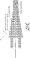
- For example, conventional optical fiber based optical couplers, such as shown in
FIG. 6 (Prior Art) are typically configured by inserting standard optical fibers (used as input fibers) into a capillary tube comprised of a material with a refractive index lower than the cladding of the input fibers. There are a number of significant disadvantages to this approach. For example, a fiber cladding- capillary tube interface becomes a light guiding interface of a lower quality than interfaces inside standard optical fibers and, therefore, can be expected to introduce optical loss. Furthermore, the capillary tube must be fabricated using a costly fluorine-doped material, greatly increasing the expense of the coupler. -
U.S. Patent No. 7,308, 173 , entitled "OPTICAL FIBER COUPLER WITH LOW LOSS AND HIGH COUPLING COEFFICIENT AND METHOD OF FABRICATION THEREOF", advantageously addressed all of the above issues by providing various embodiments of an optical fiber coupler capable of providing a low-loss, high-coupling coefficient interface between conventional optical fibers and optical waveguide devices. -
US 2013/216184 A1 relates to optical fiber coupler arrays capable of providing a low loss, high-coupling coefficient interface with high accuracy and easy alignment between a plurality of optical fibers or other optical devices. -
US 2011/0002585 A1 relates to a device to combine several mid-infrared opticalsignals from multiple optical fibers into one signal in a single optical fiber, comprising at least three input fibers comprising mid-infrared transmitting non-silica-based glass optical fibers of conventional core-clad structure, wherein the input fibers taper and fuse together to become a single output fiber. - Nevertheless, a number of challenges still remained. With the proliferation of optical devices with multiple waveguide interfaces (e.g., waveguide arrays), establishing low-loss high-accuracy connections to arrays of low or high NA waveguides often was problematic, especially because the spacing between the waveguides is very small making coupling thereto all the more difficult.
U.S. Patent No. 8,326,099 , entitled "OPTICAL FIBER COUPLER ARRAY", issued December 4, 2012, addressed the above challenge by providing, in at least a portion of the embodiments thereof, an optical fiber coupler array that provides a high-coupling coefficient interface with high accuracy and easy alignment between an optical waveguide device having a plurality of closely spaced high NA waveguide interfaces, and a plurality of optical fibers each having low numerical apertures separated by at least a fiber diameter. - The invention provides an optical fiber coupler array according to
independent claim 1. Further embodiments are provided by te dependent claims. - In the drawings, wherein like reference characters denote corresponding or similar elements throughout the various figures:
-
FIG. 1A is a schematic diagram of a side view of a first example of an optical fiber coupler array, not part of the invention, which comprises at least one vanishing core waveguide (VC waveguide), illustrated therein by way of example as a single VC waveguide, and at least one Non-VC waveguide, illustrated therein by way of example as a plurality of Non-VC waveguides, disposed symmetrically proximally to the example single VC waveguide; -
FIG. 1B is a schematic diagram of a side view of a second example of an optical fiber coupler array, not part of the invention, which comprises at least one vanishing core waveguide (VC waveguide), illustrated therein by way of example as a single VC waveguide, and at least one Non-VC waveguide, illustrated therein by way of example as a single Non-VC waveguide, disposed in parallel proximity to the example single VC waveguide, where a portion of the optical fiber coupler array has been configured to comprise a higher channel-to-channel spacing magnitude at its second (smaller) end than the corresponding channel-to-channel spacing magnitude at the second end of the optical fiber coupler array ofFIG. 1A ; -
FIG. 1C is a schematic diagram of a side view of a third example of an optical fiber coupler array, not part of the invention, which comprises a plurality of VC waveguides, and a plurality of Non-VC waveguides, disposed longitudinally and asymmetrically to one another, and where at least a portion of the plural Non-VC waveguides are of different types and/or different characteristics; -
FIG. 1D is a schematic diagram of a side view of a fourth example of an optical fiber coupler array, not part of the invention, configured for fan-in and fan-out connectivity and comprising a pair of optical fiber coupler components with a multi-core optical fiber element connected between the second (smaller sized) ends of the two optical fiber coupler components; -
FIG. 2A is a schematic diagram of a side view of a fifth example of an optical fiber coupler array, not part of the invention, which comprises a plurality of longitudinally proximal VC waveguides at least partially embedded in a single common housing structure, wherein each plural VC waveguide is spliced, at a particular first splice location, to a corresponding elongated optical device (such as an optical fiber), at least a portion of which extends outside the single common housing structure by a predetermined length, and wherein each particular first splice location is disposed within the single common housing structure; -
FIG. 2B is a schematic diagram of a side view of a sixth example of an optical fiber coupler array, not part of the invention, which comprises a plurality of longitudinally proximal VC waveguides at least partially embedded in a single common housing structure, wherein each plural VC waveguide is spliced, at a particular second splice location, to a corresponding elongated optical device (such as an optical fiber), at least a portion of which extends outside the single common housing structure by a predetermined length, and wherein each particular second splice location is disposed at an outer cross-sectional boundary region of the single common housing structure; -
FIG. 2C is a schematic diagram of a side view of a seventh example of an optical fiber coupler array, not part of the invention, which comprises a plurality of longitudinally proximal VC waveguides at least partially embedded in a single common housing structure, wherein each plural VC waveguide is spliced, at a particular third splice location, to a corresponding elongated optical device (such as an optical fiber), at least a portion of which extends outside the single common housing structure by a predetermined length, and wherein each particular third splice location is disposed outside the single common housing structure; -
FIG. 2D is a schematic diagram of a cross-sectional view of an alternative optical fiber coupler array, not part of the invention, comprising a plurality of longitudinally proximal VC waveguides at least partially embedded in a single common housing structure, that is configured at its second end, to increase, improve, and/or optimize optical coupling to a free-space-based optical device; -
FIG. 3A is a schematic diagram of a cross-sectional view of a first alternative, not part of the invention, of the optical fiber coupler arrays ofFIGs. 1D to 2D , above, and optionally comprising a fiducial element operable to provide a visual identification of waveguide arrangement / characteristics (such as alignment), which may be disposed in one of several categories of cross-sectional regions; -
FIG. 3B is a schematic diagram of a cross-sectional view of a first alternative, not part of the invention, of the optical fiber coupler array ofFIG. 1A , above, in which at least one VC waveguide, illustrated therein by way of example as a single VC waveguide, is positioned along a central longitudinal axis of the single common housing structure, and surrounded by a plurality of parallel proximal symmetrically positioned Non-VC waveguides; -
FIG. 3C is a schematic diagram of a cross-sectional view of a first alternative, not part of the invention, of the optical fiber coupler array ofFIG. 3B above, in which a volume of the single common housing structure medium surrounding the sections of all of the waveguides embedded therein, exceeds a total volume of the inner and outer cores of the section of the VC waveguide that is embedded within the single common housing structure; -
FIG. 3D is a schematic diagram of a cross-sectional view of a second alternative, not part of the invention, of the optical fiber coupler array ofFIG. 3B above, in which the at least one VC waveguide positioned along the central longitudinal axis of the single common housing structure comprises a plurality of VC waveguides, and wherein a volume of the single common housing structure medium surrounding the sections of all of the waveguides embedded therein, exceeds a total volume of the inner and outer cores of the sections of the plural VC waveguides that are embedded within the single common housing structure; -
FIG. 3E is a schematic diagram of a cross-sectional view of a first alternative, not part of the invention, of the optical fiber coupler array ofFIG. 3D , further comprising a central waveguide channel operable to provide optical pumping functionality therethrough; -
FIG. 3F is a schematic diagram of a cross-sectional view of a second alternative, not part of the invention, of the optical fiber coupler array ofFIG. 3D , in which the VC waveguide that is positioned along the central longitudinal axis of the single common housing structure, is of a different type, and/or comprises different characteristics from the remaining plural VC waveguides, which, if selected to comprise enlarged inner cores, may be advantageously utilized for increasing or optimizing optical coupling to different types of optical pump channels of various optical devices; -
FIG. 3G is a schematic diagram of a cross-sectional view of a third alternative, not part of the invention, of the optical fiber coupler array ofFIG. 3B above, in which at least one VC waveguide, illustrated therein by way of example as a single VC waveguide, is positioned as a side-channel, off-set from the central longitudinal axis of the single common housing structure, such that this embodiment of the optical fiber coupler array may be readily used as a fiber optical amplifier and or a laser, when spliced to a double-clad optical fiber having a non-concentric core for improved optical pumping efficiency; -
FIG. 3H is a schematic diagram of a cross-sectional view of a first alternative, not part of the invention, of the optical fiber coupler array ofFIG. 3G , above, in which the at least one VC waveguide, illustrated therein by way of example as a side-channel off-center positioned single VC waveguide, comprises polarization maintaining properties and comprises a polarization axis that is aligned with respect to its transverse off-center location; -
FIG. 3I is a schematic diagram of a cross-sectional view of a fourth alternative, not part of the invention, of the optical fiber coupler array ofFIG. 3B , above, wherein each of the centrally positioned single VC waveguide, and the plural Non-VC waveguides, comprises polarization maintaining properties (shown by way of example only as being induced by rod stress members and which may readily and alternately be induced by various other stress or equivalent designs), and a corresponding polarization axis, where all of the polarization axes are aligned to one another; -
FIG. 3J is a schematic diagram of a cross-sectional view of a first alternative, not part of the invention, of the optical fiber coupler array ofFIG. 3I , above, in which the polarization maintaining properties of all of the waveguides result only from a non-circular cross-sectional shape of each waveguide's core (or outer core in the case of the VC waveguide), shown by way of example only as being at least in part elliptical, and optionally comprising at least one waveguide arrangement indication element, positioned on an outer region of the single common housing structure, representative of the particular cross-sectional geometric arrangement of the optical coupler array's waveguides, such that a particular cross-sectional geometric waveguide arrangement may be readily identified from at least one of a visual and physical inspection of the single common coupler housing structure, the waveguide arrangement indication element being further operable to facilitate passive alignment of a second end of the optical coupler array to at least one optical device; -
FIG. 3K is a schematic diagram of a cross-sectional view of a fifth alternative, not part of the invention, of the optical fiber coupler array ofFIG. 3B , above, wherein the centrally positioned single VC waveguide, comprises polarization maintaining properties (shown by way of example only as being induced by rod stress members and which may readily and alternately be induced by various other stress or equivalent designs), and a corresponding polarization axis, and optionally comprising a plurality of optional waveguide arrangement indication elements of the same or of a different type, as described in connection withFIG. 3J ; -
FIG. 3L is a schematic diagram of a cross-sectional view of a second alternative, not part of the invention, of the optical fiber coupler array ofFIG. 3I , above, in which the single common housing structure comprises a cross section having a non-circular geometric shape (shown by way of example as a hexagon), and in which the polarization axes of the waveguides are aligned to one another and to the single common housing structure cross-section's geometric shape, and optionally further comprises a waveguide arrangement indication element, as described in connection withFIG. 3J ; -
FIG. 4 is a schematic isometric view diagram illustrating an example connection, not part of the invention, of a second end (i.e. "tip") of the optical fiber coupler array, in the process of connecting to plural vertical coupling elements of an optical device in a proximal open air optical coupling alignment configuration, that may be readily shifted into a butt-coupled configuration through full physical contact of the optical fiber coupler array second end and the vertical coupling elements; -
FIG. 5 is a schematic isometric view diagram illustrating an example connection, not part of the invention, of a second end (i.e. "tip") of the optical fiber coupler array connected to plural edge coupling elements of an optical device in a butt-coupled configuration, that may be readily shifted into one of several alternative coupling configurations, including a proximal open air optical coupling alignment configuration, and or an angled alignment coupling configuration; -
FIG. 6 is a schematic diagram of a cross-sectional view of a prior art optical fiber coupler having various drawbacks and disadvantages readily overcome by the various examples of the optical fiber coupler array ofFIGs. 1A to 5 ; and -
FIG. 7 is a schematic diagram, in various views, of a flexible pitch reducing optical fiber array (PROFA) coupler according to the invention. - It is important to note that packaging of photonic integrated circuits (PICs) with low vertical profile (perpendicular to the PIC plane) is desirable for a variety of applications, including optical communications and sensing. While this is easily achievable for edge couplers, surface couplers may require substantial vertical length.
- Accordingly, it would be advantageous to provide various embodiments of a pitch reducing optical fiber array (PROFA)-based flexible optical fiber coupler array component that may be configured and possibly optimized to comprise a structure that maintains all channels discretely with sufficiently low crosstalk, while providing enough flexibility to accommodate low profile packaging. It would further be desirable to provide a PROFA-based flexible optical fiber coupler array component comprising a flexible portion to provide mechanical isolation of a "PROFA-PIC interface" from the rest of the PROFA, resulting in increased stability with respect to environmental fluctuations, including temperature variations and mechanical shock and vibration. It would be additionally desirable to provide a PROFA-based flexible optical fiber coupler array comprising multiple coupling arrays, each having multiple optical channels, combined together to form an optical multi-port input/output (IO) interface.
- Certain embodiments are directed to an optical fiber coupler array capable of providing a low-loss, high-coupling coefficient interface with high accuracy and easy alignment between a plurality of optical fibers (or other optical devices) with a first channel-to-channel spacing, and an optical device having a plurality of waveguide interfaces with a second, smaller channel-to-channel spacing. Advantageously, in various embodiments, each of a larger size end and a smaller size end of the optical fiber coupler array is configurable to have a correspondingly different (i.e., larger vs. smaller) channel-to-channel spacing, where the respective channel-to-channel spacing at each of the optical coupler array's larger and smaller ends may be readily matched to a corresponding respective first channel-to-channel spacing of the plural optical fibers at the larger optical coupler array end, and to a second channel-to-channel spacing of the optical device plural waveguide interfaces at the smaller optical coupler array end.
- In various examples and embodiments thereof, the optical coupler array includes a plurality of waveguides (at least one of which may optionally be polarization maintaining), that comprises at least one gradually reduced "vanishing core fiber", at least in part embedded within a common housing structure. Alternatively, in various additional embodiments thereof, the coupler array may be configured for utilization with at least one of an optical fiber amplifier and an optical fiber laser.
- Each of the various examples and embodiments of the optical coupler array advantageously comprises at least one "vanishing core" (VC) fiber waveguide, described, for example, below in connection with a
VC waveguide 30A of theoptical coupler array 10A ofFIG. 1A . - It should also be noted that the term "optical device" as generally used herein, applies to virtually any single channel or multi-channel optical device, or to any type of optical fiber, including, but not being limited to, standard / conventional optical fibers. For example, optical devices with which the coupler array may advantageously couple may include, but are not limited to, one or more of the following:
- a free-space-based optical device,
- an optical circuit having at least one input/output edge coupling port,
- an optical circuit having at least one optical port comprising vertical coupling elements,
- a multi-mode (MM) optical fiber,
- a double-clad optical fiber,
- a multi-core (MC) optical fiber,
- a large mode area (LMA) fiber,
- a double-clad multi-core optical fiber,
- a standard / conventional optical fiber,
- a custom optical fiber, and/or
- an additional optical coupler array.
- In addition, while the term "fusion splice" is utilized in the various descriptions of the coupler array provided below, in reference to interconnections between various optical coupler array components, and connections between various optical coupler array components and optical device(s), it should be noted, that any other form of waveguide or other coupler array component connectivity technique or methodology may be readily selected and utilized as a matter of design choice or necessity, without departing from the spirit of the invention, including but not limited to mechanical connections.
- Referring now to
FIG. 1A , a first example of an optical fiber coupler array is shown as anoptical coupler array 10A, which comprises acommon housing structure 14A (described below), at least one VC waveguide, shown inFIG. 1A by way of example, as asingle VC waveguide 30A, and at least one Non-VC waveguide, shown inFIG. 1A by way of example, as a pair ofNon-VC waveguides 32A-1, 32A-2, each positioned symmetrically proximally to one of the sides of the examplesingle VC waveguide 30A, wherein the section of theVC waveguide 30A, located between positions B and D ofFIG. 1A is embedded in thecommon housing structure 14A. - Before describing the
coupler array 10A and its components in greater detail, it would be useful to provide a detailed overview of theVC waveguide 30A, which is advantageously utilized in each of the various examples of the coupler arrays ofFIGs. 1A to 5 . - The
VC waveguide 30A has a larger end (proximal to position B shown inFIG. 1A ), and a tapered, smaller end (proximal to position C shown inFIG. 1A ), and comprises aninner core 20A (comprising a material with an effective refractive index of N-1), anouter core 22A (comprising a material with an effective refractive index of N-2, smaller than N-1), and acladding 24A (comprising a material with an effective refractive index of N-3, smaller than N- 2). - Advantageously, the
outer core 22A serves as the effective cladding at theVC waveguide 30A large end at which theVC waveguide 30A supports "M1" spatial propagating modes within theinner core 20A, where M1 is larger than 0. The indices of refraction N-1 and N-2, are preferably chosen so that the numerical aperture (NA) at theVC waveguide 30A large end matches the NA of an optical device (e.g. an optical fiber) to which it is connected (such as anoptical device 34A-1, for example, comprising a standard / conventional optical fiber connected to theVC waveguide 30A at aconnection position 36A-1 (e.g., by a fusion splice, a mechanical connection, or by other fiber connection designs), while the dimensions of the inner and outer cores (20A, 22A), are preferably chosen so that the connected optical device (e.g., theoptical device 34A-1), has substantially the same mode field dimensions (MFD). Here and below we use mode field dimensions instead of commonly used mode field diameter (also MFD) due to the case that the cross section of the VC or Non-VC waveguides may not be circular, resulting in a non-circular mode profile. Thus, the mode field dimensions include both the mode size and the mode shape and equal to the mode field diameter in the case of a circularly symmetrical mode. - During fabrication of the
coupler array 10A from an appropriately configured preform (comprising theVC waveguide 30A preform having the corresponding inner andouter cores cladding 24A), as thecoupler array 10A preform is tapered in accordance with at least one predetermined reduction profile, theinner core 20A becomes too small to support all M1 modes. The number of spatial modes, supported by the inner core at the second (tapered) end is M2, where M2 < M1. In the case of a single mode waveguide, where M1 = 1 (corresponding to 2 polarization modes), M2 = 0, meaning that inner core is too small to support light propagation. TheVC waveguide 30A then acts as if comprised a fiber with a single core of an effective refractive index close to N-2, surrounded by a cladding of lower index N-3. - During fabrication of the
coupler array 10A, a channel-to-channel spacing S-1 at thecoupler array 10A larger end (at position B,FIG. 1A ), decreases in value to a channel-to-channel spacing S-2 at thecoupler array 10A smaller end (at position C,FIG. 1A ), in proportion to a draw ratio selected for fabrication, while the MFD value (or the inversed NA value of theVC waveguide 30A) can be either reduced, increased or preserved depending on a selected differences in refractive indices, (N-1 - N-2) and (N-2 - N-3), which depends upon the desired application for theoptical coupler array 10A, as described below. - The capability of independently controlling the channel-to-channel spacing and the MFD values at each end of the optical coupler array is a highly advantageous feature of certain embodiments. Additionally, the capability to match MFD and NA values through a corresponding selection of the sizes and shapes of inner 20A and outer 22A cores and values of N-1, N-2, and N-3, makes it possible to utilize the optical coupler array to couple to various waveguides without the need to use a lens.
- In various examples and embodiments thereof, the property of the VC waveguide permitting light to continue to propagate through the waveguide core along the length thereof when its diameter is significantly reduced, advantageously, reduces optical loss from interfacial imperfection or contamination, and allows the use of a wide range of materials for a medium 28A of the
common housing structure 14A (described below), including, but not limited to: - (a) non-optical materials (since the light is concentrated inside the waveguide core),
- (b) absorbing or scattering materials or materials with refractive index larger than the refractive index of standard / conventional fibers for reducing or increasing the crosstalk between the channels, and
- (c) pure-silica (e.g., the same material as is used in most standard / conventional fiber claddings, to facilitate splicing to multi-core, double-clad, or multi-mode fiber.
- Preferably, in accordance with certain examples and embodiments, the desired relative values of NA-1 and NA-2 (each at a corresponding end of the
coupler array 10A, for example, NA-1 corresponding to thecoupler array 10A large end, and NA-2 corresponding to thecoupler array 10A small end), and, optionally, the desired value of each of NA-1 and NA-2), may be determined by selecting the values of the refractive indices N1, N2, and N3 of thecoupler array 10A, and configuring them in accordance with at least one of the following relationships, selected based on the desired relative numerical aperture magnitudes at each end of thecoupler array 10A :Desired NA-1/NA-2 Relative Magnitude Corresponding Relationship bet. N1, N2, N3 NA-1 (lrg. end) > NA-2 (sm. end) (N1 - N2 > N2 - N3) NA-1 (lrg. end) = NA-2 (sm. end) (N1 - N2 = N2 - N3) NA-1 (lrg. end) < NA-2 (sm. end) (N1 - N2 < N2 - N3) - Commonly the NA of any type of fiber is determined by the following expression:

- It should be noted that when the above expression is used, the connection between the NA and the acceptance angle of the fiber is only an approximation. In particular, fiber manufacturers often quote "NA" for single-mode (SM) fibers based on the above expression, even though the acceptance angle for a single-mode fiber is quite different and cannot be determined from the indices of refraction alone.
- In accordance with certain examples and embodiments, as used herein, the various NA values are preferably determined utilizing effective indices of refraction for both ncore and ncladding, because the effective indices determine the light propagation and are more meaningful in the case of structured waveguides utilized in various examples and embodiments. Also, a transverse refractive index profile inside a waveguide may not be flat, but rather varying around the value N1, N2, N3, or N4. In addition, the transition between regions having refractive indices N1, N2, N3, and N4 may not be as sharp as a step function due to dopant diffusion or some other intentional or non-intentional factors, and may be a smooth function, connecting the values of N1, N2, N3, and N4. Coupling design or optimization may involve changing both the values of N1, N2, N3, and N4 and the sizes and shapes of the regions having respective indices.
- Returning now to
FIG. 1A , thecommon coupling structure 14A, comprises the medium 28A, in which the section of theVC waveguide 30A located between positions B and D ofFIG. 1A is embedded, and which may include, but is not limited to, at least one of the following materials: - a material, having properties prohibiting propagation of light therethrough,
- a material having light-absorbing optical properties,
- a material having light scattering optical properties,
- a material having optical properties selected such that said fourth refractive index (N-4) is greater than said third refractive index (N- 3), and/or
- a material having optical properties selected such that said fourth refractive index (N-4) is substantially equal to said third refractive index (N-3).
- At the
optical coupler array 10A large end (proximally to position B inFIG. 1A ), theVC waveguide 30A is spliced, at aparticular splice location 36A-1 (shown by way of example as positioned inside thecommon housing structure 14A), to a corresponding respective elongatedoptical device 34A-1 (for example, such as an optical fiber), at least a portion of which extends outside thecommon housing structure 14A by apredetermined length 12A, while theNon-VC waveguides 32A-1, 32A-2 are spliced, atparticular splice locations 36A-2, 36A-3, respectively (disposed outside of thecommon housing structure 14A), to corresponding respective elongatedoptical devices 34A-2, 34A-3 (such as optical fibers), and extending outside thecommon housing structure 14A by apredetermined length 12A. - Optionally, the
coupler array 10A may also include a substantiallyuniform diameter tip 16A (shown between positions C and D inFIG. 1A ) for coupling, at anarray interface 18A with theinterface 42A of anoptical waveguide device 40A. Theuniform diameter tip 16A may be useful in certain interface applications, such as for example shown inFIGs. 1D ,4 and 5 . Alternatively, thecoupler array 10A may be fabricated without thetip 16A (or have thetip 16A removed after fabrication), such that coupling with theoptical device interface 42A, occurs at acoupler array 10A interface at position C ofFIG. 1A . - In an alternative, if the
optical device 40A comprises a double-clad fiber, when the small end of thecoupler array 10A is coupled (for example, fusion spliced) to theoptical device interface 42A, at least a portion of thecommon housing structure 14A proximal to the splice position (such as at least a portion of thetip 16A), may be coated with a low index medium (not shown), extending over the splice position and up to the double-clad fiberoptical device 40A outer cladding (and optionally extending over a portion of the double-clad fiberoptical device 40A outer cladding that is proximal to the splice position). - Referring now to
FIG. 1B , a second example of the optical fiber coupler array, is shown as acoupler array 10B. Thecoupler array 10B comprises acommon housing structure 14B, at least one VC waveguide, shown inFIG. 1B by way of example, as asingle VC waveguide 30B, and at least one Non-VC waveguide, shown inFIG. 1B by way of example, as a singleNon-VC waveguide 32B, disposed in parallel proximity to theVC waveguide 30B, where a portion of theoptical coupler array 10B, has been configured to comprise a larger channel-to-channel spacing value S2' at its small end, than the corresponding channel-to-channel spacing value S2 at the small end of theoptical coupler array 10A, ofFIG. 1A . This configuration may be readily implemented by transversely cutting theoptical fiber array 10A at a position C', thus producing thecommon housing structure 14B that is shorter than thecommon housing structure 14A and resulting in a new, largerdiameter array interface 18B, having the larger channel-to-channel spacing value S2'. - Referring now to
FIG. 1C , a third example of the optical fiber coupler array, is shown as acoupler array 10C. Thecoupler array 10C comprises a plurality of VC waveguides, shown inFIG. 1C asVC waveguides 30C-1, and 30C-2, and a plurality of Non-VC waveguides, shown inFIG. 1C asNon-VC waveguides 32C-1, 32C-2, and 32C-a, all disposed longitudinally and asymmetrically to one another, wherein at least a portion of the plural Non-VC waveguides are of different types and/or different characteristics (such as single mode or multimode or polarization maintaining etc.) - for example,Non-VC waveguides 32C-1, 32C-2 are of a different type, or comprise different characteristics from theNon-VC waveguide 32C-a. Additionally, any of the VC or Non-VC waveguides (such as, for example, theNon-VC waveguide 32C-a) can readily extend beyond thecoupler array 10C common housing structure by any desired length, and need to be spliced to an optical device proximally thereto. - Referring now to
FIG. 1D , a fourth example of the optical fiber coupler array that is configured for multi-core fan-in and fan-out connectivity, and shown as acoupler array 50. Thecoupler array 50 comprises a pair of optical fiber coupler array components (10D-1 and 10D-2), with a multi-coreoptical fiber element 52 connected (e.g., by fusion splicing at positions 54-1 and 54-2) between the second (smaller sized) ends of the two optical fiber coupler array components (10D-1, 10D-2). Preferably, at least one of the VC waveguides in each of the coupler array components (10D-1, 10D-2) is configured to increase or maximize optical coupling to a corresponding selected core of the multi-coreoptical fiber element 52, while decreasing or minimizing optical coupling to all other cores thereof. - Referring now to
FIG. 2A , a fifth example of the optical fiber coupler array, is shown as acoupler array 100A. Thecoupler array 100A comprises a plurality of longitudinally proximal VC waveguides at least partially embedded in a singlecommon housing structure 104A, shown by way of example only, asplural VC waveguides 130A-1, 130A-2. Eachplural VC waveguide 130A-1, 130A-2 is spliced, at aparticular splice location 132A-1, 132A-2, respectively, to a corresponding respective elongatedoptical device 134A-1, 134A-2 (such as an optical fiber), at least a portion of which extends outside thecommon housing structure 104A by apredetermined length 102A, and wherein eachparticular splice location 132A-1, 132A-2 is disposed within thecommon housing structure 104A. - Referring now to
FIG. 2B , a sixth example of the optical fiber coupler array, is shown as acoupler array 100B. - The
coupler array 100B comprises a plurality of longitudinally proximal VC waveguides at least partially embedded in a singlecommon housing structure 104B, shown by way of example only, asplural VC waveguides 130B-1, 130B-2. Eachplural VC waveguide 130B-1, 130B-2 is spliced, at aparticular splice location 132B-1, 132B-2, respectively, to a corresponding respective elongatedoptical device 134B-1, 134B-2 (such as an optical fiber), at least a portion of which extends outside thecommon housing structure 104B by apredetermined length 102B, and wherein eachparticular splice location 132B-1, 132B-2 is disposed at an outer cross-sectional boundary region of thecommon housing structure 104B. - Referring now to
FIG. 2C , a seventh example of the optical fiber coupler array, is shown as acoupler array 100C. - The
coupler array 100C comprises a plurality of longitudinally proximal VC waveguides at least partially embedded in a singlecommon housing structure 104C, shown by way of example only, asplural VC waveguides 130C-1, 130C-2. Eachplural VC waveguide 130C-1, 130C-2 is spliced, at aparticular splice location 132C-1, 132C-2, respectively, to a corresponding respective elongatedoptical device 134C-1, 134C-2 (such as an optical fiber), at least a portion of which extends outside thecommon housing structure 104C by apredetermined length 102C, and wherein eachparticular splice location 132C-1, 132C-2 is disposed outside of thecommon housing structure 104C. - Referring now to
FIG. 2D , an alternative of the optical fiber coupler array, is shown as acoupler array 150. Thecoupler array 150 comprises a plurality of longitudinally proximal VC waveguides at least partially embedded in a single common housing structure, that is configured at its second end, to increase or optimize optical coupling to a free-space-basedoptical device 152. The free-space-basedoptical device 152 may comprise alens 154 followed by an additionaloptical device component 156, which may comprise, by way of example, a MEMS mirror or volume Bragg grating. The combination of the coupler and the free-space-basedoptical device 152 may be used as an optical switch or WDM device for spectral combining or splitting oflight signals 160b (representative of thelight coupler array 150output light signals 160a after they have passed through thelens 154.) In this case, one of the fibers may be used as an input and all others for an output or vice versa. - Prior to describing the various examples shown in
FIGs. 3A to 3L in greater detail, it should be understood that whenever a "plurality" or "at least one" coupler component/element is indicated below, the specific quantity of such coupler components/elements that may be provided in the corresponding example of the coupler array, may be selected as a matter of necessity, or design choice (for example, based on the intended industrial application of the coupler array). Accordingly, in the variousFIGs. 3A to 3L , single or individual coupler array components/elements are identified by a single reference number, while each plurality of the coupler component/elements is identified by a reference number followed by a "(1..n)" designation, with "n" being a desired number of plural coupler elements/components (and which may have a different value in any particular coupler array example described below). - Also, all the waveguides VC and Non-VC are shown with a circular cross-section of the inner and outer core and cladding only by example. Other shapes of the cross-sections of the inner and outer core and cladding (for example, hexagonal, rectangular or squared) may be utilized without departure from the current invention. The specific choice of shape is based on various requirements, such as channel shape of the optical device, channel positional geometry (for example, hexagonal, rectangular or square lattice), or axial polarization alignment mode.
- Similarly, unless otherwise indicated below, as long as various relationships set forth below (for example, the relative volume relationship set forth below with respect to
optical coupler arrays 200C and 200D ofFIGs. 3C and 3D , respectively, and the feature, set forth below in connection with thecoupler array 200H ofFIG. 3H , that thePM VC waveguide 204H is positioned longitudinally off-centered transversely from thecoupler array 200H central longitudinal axis), are adhered to, the sizes, relative sizes, relative positions and choices of composition materials, are not limited to the example sizes, relative sizes, relative positions and choices of composition materials, indicated below in connection with the detailed descriptions of the coupler array examples ofFIGs. 3A to 3L , but rather they may be selected by one skilled in the art as a matter of convenience or design choice. - Finally, it should be noted that each of the various single common
housing structure components 202A to 202L, of thevarious coupler arrays 200A to 200L ofFIGs. 3A to 3L , respectively, may be composed of a medium having the refractive index N-4 value in accordance with an applicable one of the above-described relationships with the values of other coupler array component refractive indices N-1, N-2, and N-3, and having properties and characteristics selected from the various contemplated example medium composition parameters described above in connection with medium 28A ofFIG. 1A . - Referring now to
FIG. 3A , a first alternative of the optical fiber coupler arrays ofFIGs. 1D to 2D , is shown as acoupler array 200A in which all waveguides are VC waveguides. Thecoupler array 200A comprises a singlecommon housing 202A, and plurality ofVC waveguides 204A-(1..n), with n being equal to 19 by way of example only, disposed centrally along the central longitudinal axis of thehousing 202A. Thecoupler array 200A may also comprise an optional at least onefiducial element 210A, operable to provide one or more useful properties to the coupler array, including, but not limited to: - enabling visual identification (at at least one of the coupler array's ends) of the coupler array waveguide arrangement; and
- facilitating passive alignment of at least one of the coupler array ends to at least one optical device.
- Furthermore, when deployed in optical coupler arrays that comprise at least one polarization maintaining VC waveguide (such as the optical coupler arrays described below in connection with
FIGs. 3H - 3L ), a fiducial element is further operable to: - enable visual identification of the optical coupler array's particular polarization axes alignment mode (such as described below in connection with
FIGs. 3H - 3L ); and - serve as a geometrically positioned reference point for alignment thereto, of one or more polarization axis of PM waveguides in a particular optical coupler array.
- The
fiducial element 210A may comprise any of the various types of fiducial elements known in the art, for example, it may be a dedicated elongated element positioned longitudinally within thecommon housing structure 202A in one of various cross-sectional positions (such as positions X or Y, shown inFIG. 3A . Alternatively, thefiducial element 210A may comprise a dedicated channel not used for non-fiducial purposes, for example, replacing one of thewaveguides 204A-(1..n), shown by way of example only at position Z inFIG. 3A . - Referring now to
FIG. 3B , a first alternative of the opticalfiber coupler array 10A ofFIG. 1A , above, is shown as acoupler array 200B, that comprises asingle housing structure 202B, and at least one VC waveguide, shown inFIG. 3B by way of example as aVC waveguide 204B, and a plurality ofNon-VC waveguides 206B-(1..n), with n being equal to 18 by way of example only. TheVC waveguide 204B is positioned along a central longitudinal axis of thecommon housing structure 202B, and circumferentially and symmetrically surrounded by proximal parallel pluralNon-VC waveguides 206B- (1..n). - Referring now to
FIG. 3C , a first alternative of the opticalfiber coupler array 200B ofFIG. 3B , above, is shown as a coupler array 200C that comprises asingle housing structure 202C, aVC waveguide 204C, and a plurality ofNon-VC waveguides 206C-(1..n), with n being equal to 18 by way of example only. TheVC waveguide 204C is positioned along a central longitudinal axis of thecommon housing structure 202C, and circumferentially and symmetrically surrounded by proximal parallel pluralNon-VC waveguides 206C-(1..n). The coupler array 200C is configured such that a volume of thecommon housing structure 202C medium, surrounding the sections of all of the waveguides embedded therein (i.e., theVC waveguide 204C and the pluralNon-VC waveguides 206C-(1..n)), exceeds a total volume of the inner and outer cores of the section of theVC waveguide 204C that is embedded within the singlecommon housing structure 202C. - Referring now to
FIG. 3D , a first alternative of the optical fiber coupler array 200C ofFIG. 3C , above, is shown as acoupler array 200D that comprises asingle housing structure 202D, a plurality ofVC waveguides 204D-(1..N), with N being equal to 7 by way of example only, and a plurality ofNon-VC waveguides 206D-(1..n), with n being equal to 12 by way of example only. Theplural VC waveguides 204D-(1..N) are positioned along a central longitudinal axis of thecommon housing structure 202D, and circumferentially and symmetrically surrounded by proximal parallel plural Non-VC waveguides 206D-(1..n). Thecoupler array 200D is configured such that a volume of thecommon housing structure 202D medium, surrounding the sections of all of the waveguides embedded therein (e.g., theplural VC waveguides 204D-(1..N), and the pluralNon-VC waveguides 206D-(1..n)), exceeds a total volume of the inner and outer cores of the section of theplural VC waveguides 204D-(1..N) that are embedded within the singlecommon housing structure 202D. - Referring now to
FIG. 3E , a first alternative of the opticalfiber coupler array 200D ofFIG. 3D , above, is shown as acoupler array 200E, that comprises asingle housing structure 202E, a plurality ofVC waveguides 204E-(1..N), with N being equal to 6 by way of example only, a plurality ofNon-VC waveguides 206E-(1..n), with n being equal to 12 by way of example only, and a separate singleNon-VC waveguide 206E'. TheNon-VC waveguide 206E', is preferably operable to provide optical pumping functionality therethrough, and is positioned along a central longitudinal axis of thecommon housing structure 202E and circumferentially and symmetrically surrounded by proximal parallelplural VC waveguides 204E-(1..N), that are in turn circumferentially and symmetrically surrounded by proximal parallel plural Non-VC waveguides 206E-(1..n). - Referring now to
FIG. 3F , a second alternative of the opticalfiber coupler array 200B ofFIG. 3B , above, is shown as acoupler array 200F, that comprises asingle housing structure 202F, a plurality ofVC waveguides 204F-(1..N), with N being equal to 6 by way of example only, a separatesingle VC waveguide 204F', and a plurality ofNon-VC waveguides 206F-(1..n), with n being equl to 12 by way of example only, that preferably each comprise enlarged inner cores of sufficient diameter to increase or optimize optical coupling to different types of optical pump channels of various optical devices, to which thecoupler array 200F may be advantageously coupled. TheVC waveguide 204F', is positioned along a central longitudinal axis of thecommon housing structure 202F, and circumferentially and symmetrically surrounded by proximal parallelplural VC waveguides 204F-(1..N), that are in turn circumferentially and symmetrically surrounded by proximal parallel plural Non-VC waveguides 206F-(1..n). - Referring now to
FIG. 3G , a third alternative of the opticalfiber coupler array 200B ofFIG. 3B , above, is shown as acoupler array 200G, that comprises asingle housing structure 202G, and at least one VC waveguide, shown inFIG. 3G by way of example as aVC waveguide 204G, and a plurality ofNon-VC waveguides 206G-(1..n), with n being equal to 18 by way of example only. TheVC waveguide 204G is positioned as a side-channel, off-set from the central longitudinal axis of the singlecommon housing structure 202G, such that opticalfiber coupler array 200G may be readily used as a fiber optical amplifier and or a laser, when spliced to a double-clad optical fiber (not shown) having a non-concentric core for improved optical pumping efficiency. It should be noted that because a double-clad fiber is a fiber in which both the core and the inner cladding have light guiding properties, most optical fiber types, such as SM, MM, LMA, or MC (multi-core), whether polarization maintaining or not, and even standard (e.g., conventional) single mode optical fibers, can be converted into a double-clad fiber by coating (or recoating) the fiber with a low index medium (forming the outer cladding). - Optionally, when the second end of the
coupler array 200G is spliced to a double-clad fiber (not shown), at least a portion of thecommon housing structure 202G proximal to the splice point with the double-clad fiber (not-shown), may be coated with a low index medium extending over the splice point and up to the double-clad fiber's outer cladding (and optionally extending over a portion of the outer cladding that is proximal to the splice point). - Referring now to
FIGs. 3H to 3L , in various alternative examples of the optical coupler, at least one of the VC waveguides utilized therein, and, in certain embodiments, optionally at least one of the Non-VC waveguides, may comprise a polarization maintaining (PM) property. By way of example, the PM property of a VC waveguide may result from a pair of longitudinal stress rods disposed within the VC waveguide outside of its inner core and either inside, or outside, of the outer core (or through other stress elements), or the PM property may result from a noncircular inner or outer core shape, or from other PM-inducing optical fiber configurations (such as in bow-tie or elliptically clad PM fibers). In various examples of the optical fiber in which at least one PM waveguide (VC and/or Non-VC) is utilized, an axial alignment of the PM waveguides (or waveguide), in accordance with a particular polarization axes alignment mode may be involved. - In accordance with certain examples a polarization axes alignment mode may comprise, but is not limited to, at least one of the following:
- axial alignment of a PM waveguide's polarization axis to the polarization axes of other PM waveguides in the optical coupler; when a PM waveguide is positioned off-center: axial alignment of a PM waveguide's polarization axis to its transverse cross-sectional (geometric) position within the optical coupler;
- when the single common housing structure of the optical coupler comprises a non-circular geometric shape (such as shown by way of example in
FIG. 3L ): axial alignment of a PM waveguide's polarization axis to a geometric feature of the common housing structure outer shape; - in optical coupler examples comprising one or more waveguide arrangement indicators, described below, in connection with
FIGs. 3J-3L : axial alignment of a PM waveguide's polarization axis to at least one geometric characteristic thereof; - in optical coupler examples comprising at least one
fiducial element 210A, as described above in connection withFIG. 3A : axial alignment of a PM waveguide's polarization axis to a geometric position of the at least onefiducial element 210A; - The selection of a specific type of polarization axes alignment mode for the various examples of the optical coupler is preferably governed by at least one axes alignment criterion, which may include, but which is not limited to: alignment of PM waveguides' polarization axes in a geometric arrangement that increases or maximizes PM properties thereof; and/or satisfying at least one requirement of one or more intended industrial application for the coupler array.
- Referring now to
FIG. 3H , a first alternative of the opticalfiber coupler array 200G ofFIG. 3G , above, is shown as acoupler array 200H, that comprises asingle housing structure 202H, and at least one VC waveguide, shown inFIG. 3H by way of example as aPM VC waveguide 204H having polarization maintaining properties, and a plurality ofNon-VC waveguides 206H-(1..n), with n being equal to 18 by way of example only. ThePM VC waveguide 204H is positioned as a side-channel, off-set from the central longitudinal axis of the singlecommon housing structure 202H, and comprises a polarization axis that is aligned, by way of example, with respect to the transverse off-center location of thePM VC waveguide 204H. - Referring now to
FIG. 3I , a fourth alternative of the opticalfiber coupler array 200B ofFIG. 3B , above, is shown as acoupler array 2001, that comprises asingle housing structure 2021, and at least one VC waveguide, shown inFIG. 3I by way of example as aPM VC waveguide 2041 having polarization maintaining properties, and a plurality of PM Non-VC waveguides 206I-(1..n), with n being equal to 18 by way of example only, each also having polarization maintaining properties. The PM VC waveguide 204I is positioned along a central longitudinal axis of the common housing structure 202I, and circumferentially and symmetrically surrounded by proximal parallel plural PM Non-VC waveguides 206I-(1..n). By way of example, the coupler array 200I comprises a polarization axes alignment mode in which the polarization axes of each of the PM VC waveguide 204I and of the plural PM Non-VC waveguides 2061-(1..n) are aligned to one another. The PM properties of the PM VC waveguide 204I and of the plural PM Non-VC waveguides 206I-(1..n) are shown, by way of example only, as being induced by rod stress members (and which may readily and alternately be induced by various other stress, or equivalent designs)). - Referring now to
FIG. 3J , a first alternative of the optical fiber coupler array 200I ofFIG. 3I , above, is shown as acoupler array 200J, that comprises asingle housing structure 202J, and at least one VC waveguide, shown inFIG. 3J by way of example as aPM VC waveguide 204J having polarization maintaining properties, and a plurality of PMNon-VC waveguides 206J-(1..n), with n being equal to 18 by way of example only, each also having polarization maintaining properties. ThePM VC waveguide 204J is positioned along a central longitudinal axis of thecommon housing structure 202J, and circumferentially and symmetrically surrounded by proximal parallel plural PMNon-VC waveguides 206J-(1..n). The PM properties of thePM VC waveguide 204J and of the plural PMNon-VC waveguides 206J-(1..n) are shown, by way of example only, as resulting only from a non-circular cross-sectional shape (shown by way of example only as being at least in part elliptical), of each plural PMNon-VC waveguide 206J-(1..n) core (and from a non-circular cross-sectional shape of the outer core of thePM VC waveguide 204J). - The
coupler array 200J optionally comprises at least one waveguidearrangement indication element 208J, positioned on an outer region of thecommon housing structure 202J, that is representative of the particular cross-sectional geometric arrangement of theoptical coupler array 200J waveguides (i.e., of thePM VC waveguide 204J and of the plural PMNon-VC waveguides 206J-(1..n)), such that a particular cross-sectional geometric waveguide arrangement may be readily identified from at least one of a visual and physical inspection of the commoncoupler housing structure 202J that is sufficient to examine the waveguidearrangement indication element 208J. Preferably, the waveguidearrangement indication element 208J may be configured to be further operable to facilitate passive alignment of a second end of theoptical coupler array 200J to at least one optical device (not shown). - The waveguide
arrangement indication element 208J, may comprise, but is not limited to, one or more of the following, applied to thecommon housing structure 202J outer surface: a color marking, and/or a physical indicia (such as an groove or other modification of thecommon housing structure 202J outer surface, or an element or other member positioned thereon). Alternatively, the waveguidearrangement indication element 208J may actually comprise a specific modification to, or definition of, the cross-sectional geometric shape of thecommon housing structure 202J (for example, such as a hexagonal shape of acommon housing structure 202L ofFIG. 3L , below, or another geometric shape). - By way of example, the
coupler array 200J may comprise a polarization axes alignment mode in which the polarization axes of each of thePM VC waveguide 204J and of the plural PMNon-VC waveguides 206J-(1..n) are aligned to one another, or to the waveguidearrangement indication element 208J. - Referring now to
FIG. 3K , a fifth alternative of the opticalfiber coupler array 200B ofFIG. 3B , above, is shown as acoupler array 200K, that comprises asingle housing structure 202K, and at least one VC waveguide, shown inFIG. 3K by way of example as aPM VC waveguide 204K having polarization maintaining properties, and a plurality ofNon-VC waveguides 206K-(1..n), with n being equal to 18 by way of example only. ThePM VC waveguide 204K is positioned along a central longitudinal axis of thecommon housing structure 202K, and circumferentially and symmetrically surrounded by proximal parallel plural PMNon-VC waveguides 206K-(1..n). The PM properties of thePM VC waveguide 204K are shown, by way of example only, as being induced by rod stress members (and which may readily and alternately be induced by various other stress, or equivalent approaches)). Thecoupler array 200K, may optionally comprise a plurality of waveguide arrangement indication elementsshown by way of example only, as waveguidearrangement indication elements 208K-a and 208K-b, which may each be of the same, or of a different type, as described above, in connection with the waveguidearrangement indication element 208J ofFIG. 3J . - Referring now to
FIG. 3L , a second alternative of the optical fiber coupler array 200I ofFIG. 3I , above, is shown as acoupler array 200L, that comprises asingle housing structure 202L comprising a cross section having a non-circular geometric shape (shown by way of example as a hexagon), and at least one VC waveguide, shown inFIG. 3L by way of example as aPM VC waveguide 204L having polarization maintaining properties, and a plurality of PMNon-VC waveguides 206L-(1..n), with n being equal to 18 by way of example only, each also having polarization maintaining properties. ThePM VC waveguide 204L is positioned along a central longitudinal axis of thecommon housing structure 202L, and circumferentially and symmetrically surrounded by proximal parallel plural PMNon-VC waveguides 206L-(1..n). - By way of example, the
coupler array 200L comprises a polarization axes alignment mode in which the polarization axes of each of thePM VC waveguide 204L and of the plural PMNon-VC waveguides 206L-(1..n) are aligned to one another, and to thecommon housing structure 202L cross-sectional geometric shape. The PM properties of thePM VC waveguide 204L and of the plural PMNon-VC waveguides 206L-(1..n) are shown, by way of example only, as being induced by rod stress members (and which may readily and alternately be induced by various other stress, or equivalent designs)). Thecoupler array 200K, may optionally comprise a waveguidearrangement indication element 208L-a which may comprise any of the configurations described above, in connection with the waveguidearrangement indication element 208J ofFIG. 3J . - Referring now to
FIG. 4 , a second end 302 (i.e. "tip") of the optical fiber coupler array is shown, by way of example, as being in the process of connecting to pluralvertical coupling elements 306 of anoptical device 304 in a proximal open air optical coupling alignment configuration, that may be readily shifted into a butt-coupled configuration through full physical contact of the optical fiber coupler arraysecond end 302 and thevertical coupling elements 306. - Referring now to
FIG. 5 a second end 322 (i.e. "tip") of the optical fiber coupler array is shown, by way of example, as being in the process of connecting to pluraledge coupling elements 326 of anoptical device 324 in a butt-coupled configuration, that may be readily shifted into one of several alternative coupling configuration, including a proximal open air optical coupling alignment configuration, and or an angled alignment coupling configuration. - In at least one alternative the optical coupler array (i.e., such as
optical coupler arrays 200D to 200L ofFIGS. 3C to 3L ) may be readily configured to pump optical fiber lasers, and/or optical fiber amplifiers (or equivalent devices). In an example thereof, a pumping-enabled coupler array comprises a central channel (i.e., waveguide), configured to transmit a signal (i.e., serving as a "signal channel") which will thereafter be amplified or utilized to generate lasing, and further comprises at least one additional channel (i.e., waveguide), configured to provide optical pumping functionality (i.e., each serving as a "pump channel"). In various alternative examples thereof, the pumping-enabled coupler array may comprise the following in any desired combination thereof: - at least one of the following signal channels: a single mode signal channel configured for increased or optimum coupling to a single mode amplifying fiber at at least one predetermined signal or lasing wavelength, a multimode signal channel configured for increased or optimum coupling to a multimode amplifying fiber at at least one predetermined signal or lasing wavelength, and
- at least one of the following pumping channels: a single mode pumping channel configured for increased or optimum coupling to a single mode pump source at at least one predetermined pumping wavelength, a multimode pumping channel configured for increased or optimum coupling to a multimode pump source at at least one predetermined pumping wavelength.
- Optionally, to increase or maximize pumping efficiency, the pumping-enabled coupler array may be configured to selectively utilize less than all the available pumping channels. It should also be noted that, as a matter of design choice, the pumping-enabled coupler array may be configured to comprise:
- a. At least one signal channel, each disposed in a predetermined desired position in the coupler array structure;
- b. At least one pumping channel, each disposed in a predetermined desired position in the coupler array structure; and
- c. Optionally - at least one additional waveguide for at least one additional purpose other than signal transmission or pumping (e.g., such as a fiducial marker for alignment, for fault detection, for data transmission, etc.)
- Advantageously, the pump channels could be positioned in any transverse position within the coupler, including along the central longitudinal axis. The pump channels may also comprise, but are not limited to, at least one of any of the following optical fiber types: SM, MM, LMA, or VC waveguides. Optionally, any of the optical fiber(s) being utilized as an optical pump channel (regardless of the fiber type) in the coupler may comprise polarization maintaining properties.
- In yet another example the pumping-enabled coupler array may be configured to be optimized for coupling to a double-clad fiber - in this case, the signal channel of the coupler array would be configured or optimized for coupling to the signal channel of the double-clad fiber, while each of the at least one pumping channels would be configured or optimized to couple to the inner cladding of the double-clad fiber.
- In essence, the optical coupler arrays, shown by way of various examples, may also be readily implemented as high density, multi-chanel, optical input/output (I/O) for fiber-to-chip and fiber-to-optical waveguides. The optical fiber couplers may readily comprise at least the following features:
- Dramatically reduced channel spacing and device footprint (as compared to previously known solutions)
- Scalable channel count
- All-glass optical path
- Readily butt-coupled or spliced at their high density face without the need of a lens, air gap, or a beam spreading medium
- May be fabricated through a semi-automated production process
- Broad range of customizable parameters: wavelength, mode field size, channel spacing, array configuration, fiber type.
- The optical fiber couplers may be advantageously utilized for at least the following applications.
- Coupling to waveguides:
- PIC or PCB-based (single-mode or multimode)
- Multicore fibers
- Chip edge (1D) or chip face (2D) coupling
- NA optimized for the application, factoring in:
- Packaging alignment needs
- Chip processing needs / waveguide up-tapering
- Polarization maintaining properties may be readily configured
- Coupling to chip-based devices: e.g. VCSELs, photodiodes, vertically coupled gratings
- Laser diode coupling
- High density equipment Input/Output (I/O)
- Accordingly, when implemented, the various examples of the optical fiber couplers comprise at least the following advantages, as compared to currently available competitive solutions:
- Unprecedented density
- Low-loss coupling (≤ 0.5 dB)
- Operational stability
- Form factor support
- Broad spectral range
- Matching NA
- Scalable channel count
- Polarization maintenance
- Referring now to
FIG. 7 , at least one embodiment of a flexible optical fiber coupler array according to the invention is shown as a flexible pitch reducing optical fiber array (PROFA)coupler 450. Although various features of the example PROFA coupler may be described with respect toFIG. 7 , any feature described above can be implemented in any combination with a flexible PROFA coupler. For example, any of the features described with respect toFIGs. 1A-5 may be utilized in a flexible PROFA coupler. Further, any feature described with respect toFIGs. 1A-5 may be combined with any feature described with respect toFIG. 7 . - With continued reference to
FIG. 7 , theflexible PROFA coupler 450 shown inFIG. 7 can be configured for use in applications where interconnections with low crosstalk and sufficient flexibility to accommodate low profile packaging are desired. The vanishing core approach, described herein and inU.S. Patent Application Publication No. 2013/0216184 , entitled "CONFIGURABLE PITCH REDUCING OPTICAL FIBER ARRAY", allows for the creation of a pitch reducing optical fiber array (PROFA) coupler / interconnect operable to optically couple, for example, a plurality of optical fibers to an optical device (e.g., a PIC), which can be butt-coupled to an array of vertical grating couplers (VGCs). If the cross sectional structure of thecoupler 450 has an additional layer of refractive index, N-2A, even lower than N2, as described herein and inU.S. Patent Application Publication No. 2013/0216184 , the vanishing core approach can be utilized once more to reduce the outside diameter further without substantially compromising the channel crosstalk. This further reduction can advantageously provide certain embodiments with a flexible region which has a reduced cross section between a first and second end. - In some preferred embodiments, the difference (N-2A minus N-3) is larger than the differences (N-2 minus N-2A) or (N-1 minus N-2), resulting in a high NA, bend insensitive waveguide, when the light is guided by the additional layer having refractive index N-2A. Also, in some preferred embodiments, after the outside diameter of the
coupler 450 is reduced along a longitudinal length from one end to form the flexible region, the outer diameter can then be expanded along the longitudinal length toward the second end, resulting in a lower NA waveguide with larger coupling surface area at the second end. - For example, as illustrated in
FIG. 7 , certain embodiments of anoptical coupler array 450 comprise an elongatedoptical element 1000 having afirst end 1010, asecond end 1020, and aflexible portion 1050 therebetween. Theoptical element 1000 includes acoupler housing structure 1060 and a plurality oflongitudinal waveguides 1100 embedded in thehousing structure 1060. Thewaveguides 1100 are arranged with respect to one another in a cross-sectional geometric waveguide arrangement. InFIG. 7 , the example cross-sectional geometric waveguide arrangements of thewaveguides 1100 for thefirst end 1010, thesecond end 1020, and at a location within theflexible portion 1050 are shown. The cross-sectional geometric waveguide arrangement of thewaveguides 1100 for anintermediate location 1040 between thefirst end 1010 and theflexible portion 1050 is also shown. As illustrated by the shaded regions within the cross sections and as will be described herein, light can be guided through theoptical element 1000 from thefirst end 1010 to thesecond end 1020 through theflexible portion 1050. As also shown inFIG. 7 , the result is a structure, which maintains all channels discretely with sufficiently low crosstalk, while providing enough flexibility (e.g., with the flexible portion 1050) to accommodate low profile packaging. - The level of crosstalk and/or flexibility can depend on the application of the array. For example, in some embodiments, a low crosstalk can be considered within a range from -45 dB to -35 dB, while in other embodiments, a low crosstalk can be considered within a range from -15 dB to -5 dB. Accordingly, the level of crosstalk is not particularly limited. In some embodiments, the crosstalk can be less than or equal to -55 dB, -50 dB, -45 dB, -40 dB, -35 dB, -30 dB, -25 dB, -20 dB, -15 dB, -10 dB, 0 dB, or any values therebetween (e.g., less than or equal to -37 dB, -27 dB, -17 dB, -5 dB, etc.) In some embodiments, the crosstalk can be within a range from -50 dB to -40 dB, from -40 dB to -30 dB, from -30 dB to -20 dB, from -20 dB to -10 dB, from -10 dB to 0 dB, from -45 dB to -35 dB, from -35 dB to -25 dB, from -25 dB to -15 dB, from -15 dB to -5 dB, from -10 dB to 0 dB, any combinations of these ranges, or any ranges formed from any values from -55 dB to 0 dB (e.g., from -52 dB to -37 dB, from -48 dB to -32 dB, etc.).
- The flexibility can also depend on the application of the array. For example, in some embodiments, good flexibility of the
flexible portion 1050 can comprise bending of at least 90 degrees, while in other embodiments, a bending of at least 50 degrees may be acceptable. Accordingly, the flexibility is not particularly limited. In some embodiments, the flexibility can be at least 45 degrees, 50 degrees, 55 degrees, 60 degrees, 65 degrees, 70 degrees, 75 degrees, 80 degrees, 90 degrees, 100 degrees, 110 degrees, 120 degrees, or at least any value therebetween. In some embodiments, theflexible portion 1050 can bend in a range formed by any of these values, e.g., from 45 to 55 degrees, from 50 to 60 degrees, from 60 to 70 degrees, from 70 to 80 degrees, from 80 to 90 degrees, from 90 to 100 degrees, from 100 to 110 degrees, from 110 to 120 degrees, or any combinations of these ranges, or any ranges formed by any values within these ranges (e.g., from 50 to 65 degrees, from 50 to 85 degrees, from 65 to 90 degrees, etc.) In other embodiments, theflexible portion 1050 can bend more or less than these values. Bending can typically be associated with light scattering. However, various embodiments can be configured to bend as described herein (e.g., in one of the ranges described above) and achieve relatively low crosstalk as described herein (e.g., in one of the ranges described above). - In various applications, the
flexible portion 1050 might not bend in use, however the flexibility can be desired for decoupling the first 1010 or second 1020 end from other parts of thecoupler array 450. For example, theflexible portion 1050 of theflexible PROFA coupler 450 can provide mechanical isolation of the first end 1010 (e.g., a PROFA-PIC interface) from the rest of the PROFA, which results in increased stability with respect to environmental fluctuations, including temperature variations and mechanical shock and vibration. - In the embodiment shown in
FIG. 7 , thecoupler array 450 is configured to optically couple with a plurality ofoptical fibers 2000 and/or with anoptical device 3000. Theoptical fibers 2000 andoptical device 3000 can include any of those described herein. Thecoupler array 450 can couple with theoptical fibers 2000 via the plurality ofwaveguides 1100 at thefirst end 1010. In addition, thecoupler array 450 can couple with theoptical device 3000 via the plurality ofwaveguides 1100 at thesecond end 1020. As described herein, the plurality ofwaveguides 1100 comprises at least oneVC waveguide 1101.FIG. 7 illustrates all of thewaveguides 1100 as VC waveguides. However, one or more Non-VC waveguides may also be used. In addition,FIG. 7 illustrates 7 VC waveguides, yet any number of VC and/or Non-VC waveguides can be used. - As also shown in the cross sections, each of the
waveguides 1100 is disposed at an individual corresponding cross-sectional geometric position, relative to other waveguides of the plurality ofwaveguides 1100. AlthoughFIG. 7 shows a waveguide surrounded by 6 other waveguides, the cross-sectional geometric waveguide arrangement is not limited and can include any arrangement known in the art or yet to be developed including any of those shown inFIGs. 3A-3L . - As described herein, the
VC waveguide 1101 comprises an inner core (e.g., an inner vanishing core) 1110, anouter core 1120, and anouter cladding 1130 with refractive indices N-1, N-2, and N-3 respectively. As shown inFIG. 7 , theVC waveguide 1101 further comprises a secondary outer core 1122 (e.g., between theouter core 1120 and the outer cladding 1130) having refractive index N-2A. Theouter core 1120 longitudinally surrounds theinner core 1110, the secondaryouter core 1122 longitudinally surrounds theouter core 1120 with theouter cladding 1130 longitudinally surrounding the secondaryouter core 1122. In various embodiments, the relationship between the refractive indices of theinner core 1110,outer core 1120, secondaryouter core 1122, andouter cladding 1130 is advantageously N-1 > N-2 > N2-A > N-3. With such a relationship, each surrounding layer serves as an effective cladding to the layers within it (e.g., theouter core 1120 can serve as an effective cladding to theinner core 1110, and the secondaryouter core 1122 can serve as an effective cladding to the outer core 1120). Hence, the use of the secondaryouter core 1122 can provide an additional set of core and cladding. - By including the secondary
outer core 1122 with a refractive index N-2A, a higher NA is achieved (e.g., compared to without the secondary outer core 1122). In various embodiments, the difference (N-2A minus N-3) can be larger than the differences (N-2 minus N-2A) or (N-1 minus N-2) to result in a relatively high NA. Increasing NA can reduce the MFD, allowing for the channels (e.g., waveguides 1100) to be closer to each other (e.g., closer spacing between the waveguides 1100) without compromising crosstalk. Accordingly, thecoupler array 450 is reduced further in cross section (e.g., compared to without the secondary outer core 1122) providing a reduced region when light is guided by the secondaryouter core 1122. By providing a reduced region between thefirst end 1010 and thesecond end 1020, the optical fiber coupler array includes aflexible portion 1050 which is more flexible than the regions proximal to thefirst end 1010 and thesecond end 1020. - The
inner core 1110 size, theouter core 1120 size, and the spacing between thewaveguides 1100 reduce (e.g., simultaneously and gradually in some instances) along theoptical element 1000 from thefirst end 1010 to theintermediate location 1040 such that at theintermediate location 1040, theinner core 1110 size is insufficient to guide light therethrough and theouter core 1120 size is sufficient to guide at least one optical mode. Eachwaveguide 1100 has a capacity for at least one optical mode (e.g., single mode or multi-mode). For example, at thefirst end 1010, theVC waveguide 1101 can support a number of spatial modes (M1) within theinner core 1110. At theintermediate location 1040, in various embodiments, theinner core 1110 may no longer be able to support all the M1 modes (e.g., cannot support light propagation). However, in some such embodiments, at theintermediate location 1040, theouter core 1120 can be able to support all the M1 modes (and in some cases, able to support additional modes). In this example, light traveling within theinner core 1110 from thefirst end 1010 to theintermediate location 1040 can escape from theinner core 1110 into theouter core 1120 such that light can propagate within both theinner core 1110 andouter core 1120. - In addition, the
outer core 1120 size, the secondaryouter core 1122 size, and the spacing between thewaveguides 1100 reduce (e.g., simultaneously and gradually in some instances) along saidoptical element 1000, for example, from theintermediate location 1040 to theflexible portion 1050 such that at theflexible portion 1050, theouter core 1120 size is insufficient to guide light therethrough and the secondaryouter core 1122 size is sufficient to guide at least one optical mode therethrough. In certain embodiments, at theintermediate location 1040, theVC waveguide 1101 can support all the M1 modes within theouter core 1120. At theflexible portion 1050, in various embodiments, theouter core 1120 may be no longer able to support all the M1 modes (e.g., cannot support light propagation). However, in some such embodiments, at theflexible portion 1050, the secondaryouter core 1122 can be able to support all the M1 modes (and in some cases, able to support additional modes). In this example, light traveling within theouter core 1120 from theintermediate location 1040 to theflexible portion 1050 can escape from theouter core 1120 into the secondaryouter core 1122 such that light can propagate within theinner core 1110, theouter core 1120, and secondaryouter core 1122. - Furthermore, the
outer core 1120 size, the secondaryouter core 1122 size, and the spacing between thewaveguides 1100 can expand (e.g., simultaneously and gradually in some instances) along theoptical element 1000 from theflexible portion 1050 to thesecond end 1020 such that at thesecond end 1020, the secondaryouter core 1122 size is insufficient to guide light therethrough and theouter core 1120 size is sufficient to guide at least one optical mode therethrough. In certain embodiments, at thesecond end 1020, in various embodiments, the secondaryouter core 1122 may no longer be able to support all the M1 modes (e.g., cannot support light propagation). However, in some such embodiments, at thesecond end 1020, theouter core 1120 can be able to support all the M1 modes (and in some cases, able to support additional modes). In this example, light traveling within the secondaryouter core 1122 from theflexible portion 1050 to thesecond end 1020 can return and propagate only within theinner core 1110 and theouter core 1120. - It would be appreciated that light travelling from the
second end 1020 to thefirst end 1010 can behave in the reverse manner. For example, theouter core 1120 size, the secondaryouter core 1122 size, and spacing between thewaveguides 1100 reduce (e.g., simultaneously and gradually in some instances) along theoptical element 1000 from thesecond end 1020 to theflexible portion 1050 such that at theflexible portion 1050, theouter core 1120 size is insufficient to guide light therethrough and the secondaryouter core 1122 size is sufficient to guide at least one optical mode therethrough. - The reduction in cross-sectional core and cladding sizes can advantageously provide rigidity and flexibility in a
coupler array 450. Sinceoptical fibers 2000 and/or anoptical device 3000 can be fused to theends coupler array 450, rigidity at the first 1010 and second 1020 ends can be desirable. However, it can also be desirable for coupler arrays to be flexible so that they can bend to connect with low profile integrated circuits. Theflexible portion 1050 between the first 1010 and second 1020 ends can allow the first 1010 and second 1020 ends to be relatively rigid, while providing theflexible portion 1050 therebetween. The flexible portion can extend over a length of theoptical element 1000 and can mechanically isolate the first 1010 and second 1020 ends. In an embodiment, theflexible portion 1050 can mechanically isolate thefirst end 1010 from a region between theflexible portion 1050 and thesecond end 1020. In another embodimen, theflexible portion 1050 can mechanically isolate thesecond end 1020 from a region between thefirst end 1010 and theflexible portion 1050. Such mechanical isolation can provide stability to the first 1010 and second 1020 ends, e.g., with respect to environmental fluctuations, including temperature variations and mechanical shock and vibration. The length of theflexible portion 1050 is not particularly limited and can depend on the application. In some examples, the length can be in a range from 2 to 7 mm, from 3 to 8 mm, from 5 to 10 mm, from 7 to 12 mm, from 8 to 15 mm, any combination of these ranges, or any range formed from any values from 2 to 20 mm (e.g., 3 to 13 mm, 4 to 14 mm, 5 to 17 mm, etc.). In other examples, the length of theflexible portion 1050 can be shorter or longer. - At the same time, the
flexible portion 1050 can provide flexibility. In many instances, theflexible portion 1050 can have a substantially similar cross-sectional size (e.g., the cross-sectional size of the waveguides 1100) extending over the length of theflexible portion 1050. The cross-section size at theflexible portion 1050 can comprise a smaller cross-sectional size than the cross-sectional size at the first 1010 and second 1020 ends. Having a smaller cross-sectional size, thisflexible portion 1050 can be more flexible than a region proximal to the first 1010 and second 1020 ends. The smaller cross-sectional size can result from the reduction in core and cladding sizes. An optional etching post-process may be desirable to further reduce the diameter of the flexible length of theflexible PROFA coupler 450. - The
flexible portion 1050 can be more flexible than a standard SMF 28 fiber. In some examples, theflexible portion 1050 can bend at least 45 degrees, 50 degrees, 55 degrees, 60 degrees, 65 degrees, 70 degrees, 75 degrees, 80 degrees, 90 degrees, 100 degrees, 110 degrees, 120 degrees, or at least any value therebetween. In some embodiments, theflexible portion 1050 can bend in a range formed by any of these values, e.g., from 45 to 55 degrees, from 50 to 60 degrees, from 60 to 70 degrees, from 70 to 80 degrees, from 80 to 90 degrees, from 90 to 100 degrees, from 100 to 110 degrees, from 110 to 120 degrees, or any combinations of these ranges, or any ranges formed by any values within these ranges (e.g., from 50 to 65 degrees, from 50 to 85 degrees, from 65 to 90 degrees, etc.) In other examples, theflexible portion 1050 can bend more or less than these values. As described herein, in various applications, theflexible portion 1050 might not bend in use, however the flexibility can be desired for decoupling the first 1010 or second 1020 end from other parts of thecoupler array 450. - The
coupler array 450 comprises acoupler housing structure 1060. For example, thecoupler housing structure 1060 can include a common single coupler housing structure. Thecoupler housing structure 1060 comprises a medium 1140 (e.g., having a refractive index N-4) surrounding thewaveguides 1100. In some embodiments N-4 is greater than or equal to N-3. The medium 1140 can include any medium as described herein (e.g., pure-silica). The medium can also include glass such that thecoupler array 450 can be an all-glass coupler array. Thewaveguides 1100 can be embedded within themedium 1040 of thehousing structure 1060. In some examples, a total volume of the medium 1140 of thecoupler housing structure 1060 can be greater than a total volume of all the inner andouter cores coupler housing structure 1060. - Each waveguide can couple to the
optical fibers 2000 and/oroptical device 3000 at a location inside, outside, or at a boundary region of thecoupler housing structure 1060, e.g., as shown inFIGs. 1A to 2D . Because theoptical fibers 2000 andoptical device 3000 can be different at each end, thefirst end 1010 and thesecond end 1020 can each be configured for theoptical fibers 2000 oroptical device 3000 with which it is coupled. For example, the MFD of the VC waveguide at the first 1010 and/or second 1020 ends can be configured (e.g., using the sizes of the cores) to match or substantially match the MFD of theoptical fiber 2000 oroptical device 3000 with which it is coupled. In addition, the NA of the VC waveguide at the first 1010 and/or second 1020 ends can be configured (e.g., using the refractive indices) to match or substantially match the NA of theoptical fiber 2000 oroptical device 3000 with which it is coupled. The refractive indices can be modified in any way known in the art (e.g., doping the waveguide glass) or yet to be developed. In various embodiments, as described herein, the difference (N-1 minus N-2) can be greater than the difference (N-2 minus N-2A) such that the NA at thefirst end 1010 is greater than the NA at thesecond end 1020. In other embodiments, the difference (N-1 minus N-2) can be less than the difference (N-2 minus N-2A) such that the NA at thefirst end 1010 is less than the NA at thesecond end 1020. In yet other embodiments, the difference (N-1 minus N-2) can be equal to (N-2 minus N-2A) such that the NA at thefirst end 1010 is equal to the NA at thesecond end 1020. The VC waveguide can include any of the fiber types described herein including but not limited to a single mode fiber, a multi-mode fiber, and/or a polarization maintaining fiber. - The core and cladding (1110, 1120, 1122, 1130) sizes (e.g., outer cross-sectional diameters if circular or outer cross-sectional dimensions if not circular) are not particularly limited. The inner 1110 and/or outer 1120 core sizes can be in a range from 1 to 3 microns, from 2 to 5 microns, from 4 to 8 microns, from 5 to 10 microns, any combination of these ranges, or any range formed from any values from 1 to 10 microns (e.g., 2 to 8 microns, 3 to 9 microns, etc.). However, the sizes can be greater or less. For example, the inner 1110 and/or outer 1120 core sizes can range from submicrons to many microns, to tens of microns, to hundreds of microns depending, for example, on the wavelength and/or number of modes desired.
- In addition, the difference in the refractive indices (e.g., between N-1 and N-2, between N-2 and N-2A, and/or between N-2A and N-3) is not particularly limited. In some examples, the index difference can be in a range from 1.5 x 10⁻³ to 2.5 x 10⁻³, from 1.7 x 10⁻³ to 2.3 x 10⁻³, from 1.8 x 10⁻³ to 2.2 x 10⁻³, from 1.9 x 10⁻³ to 2.1 x 10⁻³, from 1.5 x 10⁻³ to 1.7 x 10⁻³, from 1.7 x 10⁻³ to 1.9 x 10⁻³, from 1.9 x 10⁻³ to 2.1 x 10⁻³, from 2.1 x 10⁻³ to 2.3 x 10⁻³ , from 2.3 x 10⁻³ to 2.5 x 10⁻³, any combination of these ranges, or any range formed from any values from 1.5 x 10⁻³ to 2.5 x 10⁻³. In other examples, the index difference can be greater or less.
- As described herein, the
optical device 3000 can include a PIC. The PIC can include an array of VGCs. Also, as described inU.S. Patent Application Publication 2012/0257857 , entitled "HIGH DENSITY OPTICAL PACKAGING HEADER APPARATUS", multiple flexible PROFA couplers (such as the coupler 450), each having multiple optical channels, can be combined together to advantageously form an optical multi-port input/output (IO) interface. As such, an optical multi-port IO interface can include a plurality of optical coupler arrays, at least one of the optical coupler arrays can include anoptical coupler array 450 as described herein.
Claims (15)
- An optical fiber coupler array (450), comprising:an elongated optical element (1000) having a first end (1010), a second end (1020), a flexible portion (1050) therebetween, and an intermediate location (1040) between said first end (1010) and said flexible portion(1050), wherein said first (1010) and second (1020) ends are configured to optically couple with a plurality of optical fibers (2000) or an optical device (3000) or combinations thereof, the optical element (1000) further comprising:a coupler housing structure (1060); anda plurality of longitudinal waveguides (1100) each arranged with respect to one another in a cross-sectional geometric waveguide arrangement, such that each waveguide (1100) is disposed at an individual corresponding cross-sectional geometric position, relative to other waveguides (1100) of the plurality of longitudinal waveguides (1100), each having a capacity for at least one optical mode, each embedded in said housing structure (1060), wherein said plurality of longitudinal waveguides (1100) comprises at least one vanishing core waveguide (1101), said at least one vanishing core waveguide (1101) comprising:an inner core (1110), having a first refractive index (N-1), andhaving an inner core (1110) size;an outer core (1120), longitudinally surrounding said inner core (1110), having a second refractive index (N-2), and having an outer core (1120) size,a secondary outer core (1122), longitudinally surrounding said outer core (1120), having a secondary refractive index (N-2A), and having secondary outer core (1122) size, andan outer cladding (1130), longitudinally surrounding said secondary outer core (1122), having a third refractive index (N-3), and having a cladding (1130) size;wherein said coupler housing structure (1060) comprises a medium (1140) having a fourth refractive index (N-4) surrounding said plurality of longitudinal waveguides (1100), wherein N-1 > N-2 > N-2A > N-3, andwherein said inner core (1110) size, said outer core (1120) size, and spacing between said plurality of longitudinal waveguides (1100) reduce along said optical element (1000) from said first end (1010) to said intermediate location (1040) such that at said intermediate location (1040),said inner core (1110) size is insufficient to guide light therethrough andsaid outer core (1120) size is sufficient to guide at least one optical mode, andwherein said outer core (1120) size, said secondary outer core (1122) size, and spacing between said plurality of longitudinal waveguides (1100) reduce along said optical element (1000) from said intermediate location (1040) to said flexible portion (1050) such that at said flexible portion (1050), said outer core (1120) size is insufficient to guide light therethrough and said secondary outer core (1122) size is sufficient to guide at least one optical mode therethrough.
- The optical fiber coupler array (450) of Claim 1, wherein said outer core (1120) size, said secondary outer core (1122) size, and spacing between said plurality of longitudinal waveguides (1100) reduce along said optical element (1000) from said second end (1020) to said flexible portion (1050) such that at said flexible portion (1050), said outer core (1120) size is insufficient to guide light therethrough and said secondary outer core (1122) size is sufficient to guide at least one optical mode therethrough.
- The optical fiber coupler array (450) of any of the preceding claims, wherein N-2A minus N-3 is greater than N-2 minus N-2A or greater than N-1 minus N-2.
- The optical fiber coupler array (450) of any of the preceding claims, wherein the flexible portion (1050) is more flexible than either of the first (1010) and second (1020) ends.
- The optical fiber coupler array (450) of any of the preceding claims, wherein the flexible portion (1050) mechanically isolates the first end (1010) from a region between the flexible portion (1050) and the second end (1020); and/or
wherein the flexible portion (1050) mechanically isolates the second end (1020) from a region between the first end (1010) and the flexible portion (1050). - The optical fiber coupler array (450) of any of the preceding claims, wherein the at least one vanishing core waveguide (1101) comprises a single mode fiber; or
wherein the at least one vanishing core waveguide (1101) comprises a multi-mode fiber; or
wherein the at least one vanishing core waveguide (1101) comprises a polarization maintaining fiber. - The optical fiber coupler array (450) of any of the preceding claims, wherein N-4 is greater than or equal to N-3.
- The optical fiber coupler array (450) of any of the preceding claims, wherein the medium (1140) comprises pure-silica.
- The optical fiber coupler array (450) of any of Claims 1-8, wherein the first end (1010) has a first numerical aperture and the second end (1020) has a second numerical aperture, wherein the first numerical aperture is greater than the second numerical aperture, and wherein N-1 minus N-2 is greater than N-2 minus N-2A.
- The optical fiber coupler array (450) of any of Claims 1-8, wherein the first end (1010) has a first numerical aperture and the second end (1020) has a second numerical aperture, wherein the first numerical aperture is less than the second numerical aperture, and wherein N-1 minus N-2 is less than N-2 minus N-2A.
- The optical fiber coupler array (450) of any Claims 1-8, wherein the first end (1010) has a first numerical aperture and the second end (1020) has a second numerical aperture, wherein the first numerical aperture is equal to the second numerical aperture, and wherein N-1 minus N-2 is equal to N-2 minus N-2A.
- The optical fiber coupler array (450) of any of the preceding claims, wherein the flexible portion (1050) is configured to bend from 80 to 90 degrees.
- The optical fiber coupler array (450) of any of Claims 1-12, wherein crosstalk between two of the plurality of longitudinal waveguides (1100) is in a range from -15 dB to -5 dB or is in a range from -25 dB to -15 dB.
- The optical fiber coupler array (450) of any of Claims 1-12, wherein crosstalk between two of the plurality of longitudinal waveguides (1100) is in a range from -35 dB to -25 dB or is in a range from -45 dB to -35 dB.
- The optical fiber coupler array (450) of any of the preceding claims, wherein the optical device (3000) comprises a photonic integrated circuit; or
wherein the optical device (3000) comprises an array of vertical grating couplers.
Applications Claiming Priority (2)
| Application Number | Priority Date | Filing Date | Title |
|---|---|---|---|
| US201562221869P | 2015-09-22 | 2015-09-22 | |
| PCT/US2016/052956 WO2017053479A1 (en) | 2015-09-22 | 2016-09-21 | Flexible optical fiber array |
Publications (3)
| Publication Number | Publication Date |
|---|---|
| EP3353579A1 EP3353579A1 (en) | 2018-08-01 |
| EP3353579A4 EP3353579A4 (en) | 2019-05-29 |
| EP3353579B1 true EP3353579B1 (en) | 2021-06-23 |
Family
ID=58387193
Family Applications (1)
| Application Number | Title | Priority Date | Filing Date |
|---|---|---|---|
| EP16849541.4A Active EP3353579B1 (en) | 2015-09-22 | 2016-09-21 | Flexible optical fiber coupler array |
Country Status (3)
| Country | Link |
|---|---|
| US (1) | US9810845B2 (en) |
| EP (1) | EP3353579B1 (en) |
| WO (1) | WO2017053479A1 (en) |
Families Citing this family (28)
| Publication number | Priority date | Publication date | Assignee | Title |
|---|---|---|---|---|
| US20090324159A1 (en) | 2008-06-26 | 2009-12-31 | Chiral Photonics, Inc. | Optical chiral fiber isolator and method of fabrication thereof |
| US20130216184A1 (en) | 2008-07-14 | 2013-08-22 | Victor Il'ich Kopp | Configurable pitch reducing optical fiber array |
| US9851510B2 (en) | 2008-07-14 | 2017-12-26 | Chiral Photonics, Inc. | Phase locking optical fiber coupler |
| US9857536B2 (en) | 2008-07-14 | 2018-01-02 | Chiral Photonics, Inc. | Optical component assembly for use with an optical device |
| US9766407B2 (en) | 2008-07-14 | 2017-09-19 | Chiral Photonics, Inc. | Untappable secure optical fiber link component |
| CN102317825A (en) | 2008-12-18 | 2012-01-11 | 手性光子公司 | Fiber Optic Diffraction Grating |
| US20110292676A1 (en) | 2010-05-28 | 2011-12-01 | Etkin | Chiral Fiber Apparatus and Method for Controllable Light Extraction from Optical Waveguides |
| US10502898B2 (en) | 2011-01-20 | 2019-12-10 | Chiral Photonics, Inc. | Chiral fiber circular polarizer |
| US20120257857A1 (en) | 2011-04-08 | 2012-10-11 | Chiral Photonics, Inc. | High Density Optical Packaging Header Apparatus |
| US20130188175A1 (en) | 2012-01-20 | 2013-07-25 | Chiral Photonics, Inc. | Configurable Chiral Fiber Tip-Positioned Sensor |
| US10914891B2 (en) | 2013-06-14 | 2021-02-09 | Chiral Photonics, Inc. | Multichannel optical coupler |
| US11966091B2 (en) | 2013-06-14 | 2024-04-23 | Chiral Photonics, Inc. | Multichannel optical coupler array |
| US10564348B2 (en) | 2013-06-14 | 2020-02-18 | Chiral Photonics, Inc. | Passive aligning optical coupler array |
| US10126494B2 (en) | 2013-06-14 | 2018-11-13 | Chiral Photonics, Inc. | Configurable polarization mode coupler |
| US9817191B2 (en) | 2013-06-14 | 2017-11-14 | Chiral Photonics, Inc. | Multichannel optical coupler array |
| US10838155B2 (en) | 2013-06-14 | 2020-11-17 | Chiral Photonics, Inc. | Multichannel optical coupler |
| US10101536B2 (en) | 2013-06-14 | 2018-10-16 | Chiral Photonics, Inc. | Multichannel optical coupler array |
| US11156781B2 (en) | 2013-06-14 | 2021-10-26 | Chiral Photonics, Inc. | Passive aligning optical coupler array |
| WO2017053479A1 (en) | 2015-09-22 | 2017-03-30 | Chiral Photonics, Inc. | Flexible optical fiber array |
| EP3387471B1 (en) | 2015-12-09 | 2022-05-04 | Chiral Photonics, Inc. | Polarization maintaining optical fiber array |
| US9885825B2 (en) | 2016-04-18 | 2018-02-06 | Chiral Photonics, Inc. | Pitch reducing optical fiber array and multicore fiber comprising at least one chiral fiber grating |
| WO2018227008A1 (en) * | 2017-06-08 | 2018-12-13 | Chiral Photonics, Inc. | Optical coupler arrays |
| US11022762B2 (en) | 2019-08-05 | 2021-06-01 | Chiral Photonics, Inc. | Optical fiber connectors for rotational alignment |
| JP7205643B2 (en) * | 2019-10-08 | 2023-01-17 | 日本電信電話株式会社 | Core position grasping method, connection method, and connection device |
| US11609376B2 (en) | 2020-02-24 | 2023-03-21 | Chiral Photonics, Inc. | Space division multiplexers |
| EP4258028A1 (en) * | 2020-12-04 | 2023-10-11 | Fujikura Ltd. | Fiber connecting body, optical communication system, optical device, and method for manufacturing fiber connecting body |
| CN114910996B (en) * | 2021-02-07 | 2023-08-25 | 北京邮电大学 | End face coupler |
| CN113301753A (en) * | 2021-06-01 | 2021-08-24 | Oppo广东移动通信有限公司 | Cover plate preparation method, cover plate and electronic equipment |
Family Cites Families (53)
| Publication number | Priority date | Publication date | Assignee | Title |
|---|---|---|---|---|
| US20020003827A1 (en) | 1998-05-01 | 2002-01-10 | Genack Azriel Zelig | Stop band laser apparatus and method |
| EP1058955A4 (en) | 1998-12-21 | 2005-09-21 | Chiral Photonics Inc | Chiral laser apparatus and method |
| JP2002536827A (en) | 1999-02-04 | 2002-10-29 | カイラル・フオトニクス・インコーポレーテツド | Apparatus and method for chiral twist type laser and filter |
| US6411635B1 (en) | 1999-03-31 | 2002-06-25 | Chiral Photonics, Inc. | Apparatus and method for mode selection in a photonic band edge laser |
| US7242702B2 (en) | 2000-01-07 | 2007-07-10 | Chiral Photonics, Inc. | Thin-film large-area coherent light source, filter and amplifier apparatus and method |
| AU2930101A (en) | 2000-01-07 | 2001-07-24 | Chiral Photonics, Inc. | Thin-film large-area coherent light source, filter and amplifier apparatus and method |
| AU2001249292A1 (en) | 2000-03-20 | 2001-10-03 | Chiral Photonics, Inc. | Chiral laser utilizing a quarter wave plate |
| US20020069676A1 (en) | 2000-12-12 | 2002-06-13 | Kopp Victor Il?Apos;Ich | Apparatus and method of manufacturing chiral fiber bragg gratings |
| US6744943B2 (en) | 2000-12-12 | 2004-06-01 | Chiral Photonics, Inc. | Add-drop filter utilizing chiral elements |
| EP1387816A4 (en) | 2001-03-14 | 2008-11-26 | Chiral Photonics Inc | Apparatus and method for fabricating chiral fiber gratings |
| AU2002254235A1 (en) | 2001-03-14 | 2002-09-24 | Chiral Photonics, Inc. | Chiral fiber bragg grating |
| US6891992B2 (en) | 2001-04-13 | 2005-05-10 | Chiral Photonics, Inc. | Configurable add-drop filter utilizing chiral fiber gratings |
| US6875276B2 (en) | 2001-06-15 | 2005-04-05 | Chiral Photonics, Inc. | Apparatus and method for fabricating layered periodic media |
| EP1456919B1 (en) | 2001-11-19 | 2007-09-26 | Chiral Photonics, Inc. | Chiral fiber laser apparatus and method |
| AU2002359634A1 (en) | 2001-12-06 | 2003-06-23 | Chiral Photonics, Inc. | Chiral in-fiber adjustable polarizer apparatus and method |
| DE60239424D1 (en) | 2001-12-06 | 2011-04-21 | Chiral Photonics Inc | CHIRAL FIBER SENSOR AND METHOD |
| US20030118285A1 (en) | 2001-12-06 | 2003-06-26 | Kopp Victor Il?Apos;Ich | Customizable chirped chiral fiber bragg grating |
| US6741631B2 (en) | 2002-03-14 | 2004-05-25 | Chiral Photonics, Inc. | Customizable apodized chiral fiber grating apparatus and method |
| US7009679B2 (en) | 2002-03-14 | 2006-03-07 | Chiral Photonics, Inc. | Chiral boardband tuning apparatus and method |
| WO2003077632A1 (en) | 2002-03-14 | 2003-09-25 | Chiral Photonics, Inc. | Extended chiral defect structure apparatus and method |
| WO2003083540A1 (en) | 2002-03-22 | 2003-10-09 | Chiral Photonics, Inc. | Long period chiral fiber grating apparatus |
| US7738109B2 (en) * | 2002-08-20 | 2010-06-15 | The Board Of Trustees Of The Leland Stanford Junior University | Fiber optic sensor using a Bragg fiber |
| US20040145704A1 (en) | 2002-11-29 | 2004-07-29 | Kopp Victor Il?Apos;Ich | Chiral laser projection display apparatus and method |
| US7095911B2 (en) | 2003-10-24 | 2006-08-22 | Chiral Photonics, Inc. | Chiral in-fiber polarizer apparatus and method |
| EP1702227A2 (en) | 2003-12-18 | 2006-09-20 | Chiral Photonics, Inc. | Optical fiber coupler with low loss and high coupling coefficient and method of fabrication thereof |
| WO2005091029A2 (en) * | 2004-03-19 | 2005-09-29 | Crystal Fibre A/S | Optical coupler devices, methods of their production and use |
| JP2008524637A (en) | 2004-10-24 | 2008-07-10 | チラル・フオトニクス・インコーポレーテツド | Chiral fiber in-polarizer apparatus and method |
| CA2523930A1 (en) | 2005-10-19 | 2007-04-19 | Itf Technologies Optiques Inc./Itf Optical Technologies Inc. | Method of making fiber optic couplers with precise positioning of fibers |
| US7463800B2 (en) | 2005-12-27 | 2008-12-09 | Chiral Photonics, Inc. | Chiral fiber grating device and method of fabrication thereof |
| US20080098772A1 (en) | 2006-10-06 | 2008-05-01 | Kopp Victor Il Ich | Method for fabricating an optical fiber assembly having at least one integral optical fiber device |
| WO2008080174A1 (en) | 2006-12-27 | 2008-07-03 | Chiral Photonics, Inc. | Single helix chiral fiber grating |
| US8457456B2 (en) | 2007-10-19 | 2013-06-04 | Chiral Photonics, Inc. | Optical fiber mode coupling device, having an optimized fiber interface and method of fabrication thereof |
| US20090324159A1 (en) | 2008-06-26 | 2009-12-31 | Chiral Photonics, Inc. | Optical chiral fiber isolator and method of fabrication thereof |
| WO2010002951A2 (en) | 2008-07-01 | 2010-01-07 | Chiral Photonics, Inc. | Distributed optical fiber detection system |
| US9857536B2 (en) | 2008-07-14 | 2018-01-02 | Chiral Photonics, Inc. | Optical component assembly for use with an optical device |
| EP2344914A4 (en) | 2008-07-14 | 2013-04-03 | Chiral Photonics Inc | Dual twist single helix optical fiber grating |
| US8463094B2 (en) | 2008-07-14 | 2013-06-11 | Chiral Photonics, Inc. | Chiral fiber polarizer |
| US9766407B2 (en) | 2008-07-14 | 2017-09-19 | Chiral Photonics, Inc. | Untappable secure optical fiber link component |
| US20130216184A1 (en) | 2008-07-14 | 2013-08-22 | Victor Il'ich Kopp | Configurable pitch reducing optical fiber array |
| WO2010009101A2 (en) | 2008-07-14 | 2010-01-21 | Chiral Photonics, Inc. | Optical fiber coupler array |
| US7983515B2 (en) | 2008-12-18 | 2011-07-19 | Chiral Photonics, Inc. | Polarization maintaining optical fiber polarizer |
| CN102317825A (en) | 2008-12-18 | 2012-01-11 | 手性光子公司 | Fiber Optic Diffraction Grating |
| US10948656B2 (en) * | 2008-12-22 | 2021-03-16 | The Government Of The United States Of America, As Represented By The Secretary Of The Navy | Fiber-based mid-IR signal combiner and method of making same |
| US20110292676A1 (en) | 2010-05-28 | 2011-12-01 | Etkin | Chiral Fiber Apparatus and Method for Controllable Light Extraction from Optical Waveguides |
| US20110293219A1 (en) | 2010-05-28 | 2011-12-01 | Gary Weiner | Chiral Fiber System and Method for Providing Configurable Light Extraction from Optical Waveguides in Accordance with at Least One Predetermined Light Extraction Profile |
| US10502898B2 (en) | 2011-01-20 | 2019-12-10 | Chiral Photonics, Inc. | Chiral fiber circular polarizer |
| US8948547B2 (en) | 2011-01-20 | 2015-02-03 | Chiral Photonics, Inc. | Multi-state polarization preserving optical fiber |
| US20120257857A1 (en) * | 2011-04-08 | 2012-10-11 | Chiral Photonics, Inc. | High Density Optical Packaging Header Apparatus |
| US20130188174A1 (en) | 2012-01-20 | 2013-07-25 | Chiral Photonics, Inc. | Configurable Chiral Fiber Sensor |
| US20130188175A1 (en) | 2012-01-20 | 2013-07-25 | Chiral Photonics, Inc. | Configurable Chiral Fiber Tip-Positioned Sensor |
| JP5990419B2 (en) * | 2012-07-09 | 2016-09-14 | 株式会社フジクラ | Optical input / output device |
| KR102025196B1 (en) * | 2012-12-03 | 2019-09-25 | 한국전자통신연구원 | optical coupling module for silicon photonics chip |
| WO2017053479A1 (en) | 2015-09-22 | 2017-03-30 | Chiral Photonics, Inc. | Flexible optical fiber array |
-
2016
- 2016-09-21 WO PCT/US2016/052956 patent/WO2017053479A1/en active Application Filing
- 2016-09-21 EP EP16849541.4A patent/EP3353579B1/en active Active
- 2016-09-21 US US15/272,216 patent/US9810845B2/en active Active
Non-Patent Citations (1)
| Title |
|---|
| None * |
Also Published As
| Publication number | Publication date |
|---|---|
| US20170227716A1 (en) | 2017-08-10 |
| US9810845B2 (en) | 2017-11-07 |
| EP3353579A4 (en) | 2019-05-29 |
| WO2017053479A1 (en) | 2017-03-30 |
| EP3353579A1 (en) | 2018-08-01 |
Similar Documents
| Publication | Publication Date | Title |
|---|---|---|
| EP3353579B1 (en) | Flexible optical fiber coupler array | |
| EP3387471B1 (en) | Polarization maintaining optical fiber array | |
| EP3535612B1 (en) | Multichannel optical coupler array | |
| US9885825B2 (en) | Pitch reducing optical fiber array and multicore fiber comprising at least one chiral fiber grating | |
| US10126494B2 (en) | Configurable polarization mode coupler | |
| US9817191B2 (en) | Multichannel optical coupler array | |
| US8712199B2 (en) | Configurable pitch reducing optical fiber array | |
| US9857536B2 (en) | Optical component assembly for use with an optical device | |
| US10101536B2 (en) | Multichannel optical coupler array | |
| US9851510B2 (en) | Phase locking optical fiber coupler | |
| US10914891B2 (en) | Multichannel optical coupler | |
| WO2018227008A1 (en) | Optical coupler arrays | |
| US10838155B2 (en) | Multichannel optical coupler | |
| WO2020068695A1 (en) | Multichannel optical coupler | |
| WO2020077285A1 (en) | Passive aligning optical coupler array | |
| US11609376B2 (en) | Space division multiplexers | |
| EP4045954A1 (en) | Multichannel optical coupler | |
| EP4288819A1 (en) | Multichannel optical coupler array | |
| US20230208546A1 (en) | Wavelength division multiplexers for space division multiplexing (sdm-wdm devices) | |
| WO2024086536A1 (en) | Wavelength division multiplexers for space division multiplexing (sdm-wdm devices) |
Legal Events
| Date | Code | Title | Description |
|---|---|---|---|
| STAA | Information on the status of an ep patent application or granted ep patent |
Free format text: STATUS: THE INTERNATIONAL PUBLICATION HAS BEEN MADE |
|
| PUAI | Public reference made under article 153(3) epc to a published international application that has entered the european phase |
Free format text: ORIGINAL CODE: 0009012 |
|
| STAA | Information on the status of an ep patent application or granted ep patent |
Free format text: STATUS: REQUEST FOR EXAMINATION WAS MADE |
|
| 17P | Request for examination filed |
Effective date: 20180417 |
|
| AK | Designated contracting states |
Kind code of ref document: A1 Designated state(s): AL AT BE BG CH CY CZ DE DK EE ES FI FR GB GR HR HU IE IS IT LI LT LU LV MC MK MT NL NO PL PT RO RS SE SI SK SM TR |
|
| AX | Request for extension of the european patent |
Extension state: BA ME |
|
| DAV | Request for validation of the european patent (deleted) | ||
| DAX | Request for extension of the european patent (deleted) | ||
| A4 | Supplementary search report drawn up and despatched |
Effective date: 20190430 |
|
| RIC1 | Information provided on ipc code assigned before grant |
Ipc: G02B 6/024 20060101ALI20190424BHEP Ipc: G02B 6/04 20060101ALI20190424BHEP Ipc: G02B 6/30 20060101ALI20190424BHEP Ipc: G02B 6/26 20060101ALI20190424BHEP Ipc: G02B 6/12 20060101ALI20190424BHEP Ipc: G02B 6/122 20060101ALI20190424BHEP Ipc: G02B 6/32 20060101ALI20190424BHEP Ipc: G02B 1/00 20060101AFI20190424BHEP Ipc: G02B 6/02 20060101ALI20190424BHEP |
|
| GRAP | Despatch of communication of intention to grant a patent |
Free format text: ORIGINAL CODE: EPIDOSNIGR1 |
|
| STAA | Information on the status of an ep patent application or granted ep patent |
Free format text: STATUS: GRANT OF PATENT IS INTENDED |
|
| INTG | Intention to grant announced |
Effective date: 20200722 |
|
| GRAJ | Information related to disapproval of communication of intention to grant by the applicant or resumption of examination proceedings by the epo deleted |
Free format text: ORIGINAL CODE: EPIDOSDIGR1 |
|
| STAA | Information on the status of an ep patent application or granted ep patent |
Free format text: STATUS: REQUEST FOR EXAMINATION WAS MADE |
|
| INTC | Intention to grant announced (deleted) | ||
| GRAP | Despatch of communication of intention to grant a patent |
Free format text: ORIGINAL CODE: EPIDOSNIGR1 |
|
| STAA | Information on the status of an ep patent application or granted ep patent |
Free format text: STATUS: GRANT OF PATENT IS INTENDED |
|
| INTG | Intention to grant announced |
Effective date: 20210120 |
|
| GRAS | Grant fee paid |
Free format text: ORIGINAL CODE: EPIDOSNIGR3 |
|
| GRAA | (expected) grant |
Free format text: ORIGINAL CODE: 0009210 |
|
| STAA | Information on the status of an ep patent application or granted ep patent |
Free format text: STATUS: THE PATENT HAS BEEN GRANTED |
|
| AK | Designated contracting states |
Kind code of ref document: B1 Designated state(s): AL AT BE BG CH CY CZ DE DK EE ES FI FR GB GR HR HU IE IS IT LI LT LU LV MC MK MT NL NO PL PT RO RS SE SI SK SM TR |
|
| REG | Reference to a national code |
Ref country code: GB Ref legal event code: FG4D |
|
| REG | Reference to a national code |
Ref country code: CH Ref legal event code: EP |
|
| REG | Reference to a national code |
Ref country code: DE Ref legal event code: R096 Ref document number: 602016059776 Country of ref document: DE Ref country code: AT Ref legal event code: REF Ref document number: 1404779 Country of ref document: AT Kind code of ref document: T Effective date: 20210715 |
|
| REG | Reference to a national code |
Ref country code: IE Ref legal event code: FG4D |
|
| REG | Reference to a national code |
Ref country code: LT Ref legal event code: MG9D |
|
| PG25 | Lapsed in a contracting state [announced via postgrant information from national office to epo] |
Ref country code: LT Free format text: LAPSE BECAUSE OF FAILURE TO SUBMIT A TRANSLATION OF THE DESCRIPTION OR TO PAY THE FEE WITHIN THE PRESCRIBED TIME-LIMIT Effective date: 20210623 Ref country code: FI Free format text: LAPSE BECAUSE OF FAILURE TO SUBMIT A TRANSLATION OF THE DESCRIPTION OR TO PAY THE FEE WITHIN THE PRESCRIBED TIME-LIMIT Effective date: 20210623 Ref country code: BG Free format text: LAPSE BECAUSE OF FAILURE TO SUBMIT A TRANSLATION OF THE DESCRIPTION OR TO PAY THE FEE WITHIN THE PRESCRIBED TIME-LIMIT Effective date: 20210923 Ref country code: HR Free format text: LAPSE BECAUSE OF FAILURE TO SUBMIT A TRANSLATION OF THE DESCRIPTION OR TO PAY THE FEE WITHIN THE PRESCRIBED TIME-LIMIT Effective date: 20210623 |
|
| REG | Reference to a national code |
Ref country code: AT Ref legal event code: MK05 Ref document number: 1404779 Country of ref document: AT Kind code of ref document: T Effective date: 20210623 |
|
| PG25 | Lapsed in a contracting state [announced via postgrant information from national office to epo] |
Ref country code: LV Free format text: LAPSE BECAUSE OF FAILURE TO SUBMIT A TRANSLATION OF THE DESCRIPTION OR TO PAY THE FEE WITHIN THE PRESCRIBED TIME-LIMIT Effective date: 20210623 Ref country code: GR Free format text: LAPSE BECAUSE OF FAILURE TO SUBMIT A TRANSLATION OF THE DESCRIPTION OR TO PAY THE FEE WITHIN THE PRESCRIBED TIME-LIMIT Effective date: 20210924 Ref country code: NO Free format text: LAPSE BECAUSE OF FAILURE TO SUBMIT A TRANSLATION OF THE DESCRIPTION OR TO PAY THE FEE WITHIN THE PRESCRIBED TIME-LIMIT Effective date: 20210923 Ref country code: SE Free format text: LAPSE BECAUSE OF FAILURE TO SUBMIT A TRANSLATION OF THE DESCRIPTION OR TO PAY THE FEE WITHIN THE PRESCRIBED TIME-LIMIT Effective date: 20210623 Ref country code: RS Free format text: LAPSE BECAUSE OF FAILURE TO SUBMIT A TRANSLATION OF THE DESCRIPTION OR TO PAY THE FEE WITHIN THE PRESCRIBED TIME-LIMIT Effective date: 20210623 |
|
| REG | Reference to a national code |
Ref country code: NL Ref legal event code: MP Effective date: 20210623 |
|
| PG25 | Lapsed in a contracting state [announced via postgrant information from national office to epo] |
Ref country code: ES Free format text: LAPSE BECAUSE OF FAILURE TO SUBMIT A TRANSLATION OF THE DESCRIPTION OR TO PAY THE FEE WITHIN THE PRESCRIBED TIME-LIMIT Effective date: 20210623 Ref country code: RO Free format text: LAPSE BECAUSE OF FAILURE TO SUBMIT A TRANSLATION OF THE DESCRIPTION OR TO PAY THE FEE WITHIN THE PRESCRIBED TIME-LIMIT Effective date: 20210623 Ref country code: NL Free format text: LAPSE BECAUSE OF FAILURE TO SUBMIT A TRANSLATION OF THE DESCRIPTION OR TO PAY THE FEE WITHIN THE PRESCRIBED TIME-LIMIT Effective date: 20210623 Ref country code: PT Free format text: LAPSE BECAUSE OF FAILURE TO SUBMIT A TRANSLATION OF THE DESCRIPTION OR TO PAY THE FEE WITHIN THE PRESCRIBED TIME-LIMIT Effective date: 20211025 Ref country code: CZ Free format text: LAPSE BECAUSE OF FAILURE TO SUBMIT A TRANSLATION OF THE DESCRIPTION OR TO PAY THE FEE WITHIN THE PRESCRIBED TIME-LIMIT Effective date: 20210623 Ref country code: EE Free format text: LAPSE BECAUSE OF FAILURE TO SUBMIT A TRANSLATION OF THE DESCRIPTION OR TO PAY THE FEE WITHIN THE PRESCRIBED TIME-LIMIT Effective date: 20210623 Ref country code: AT Free format text: LAPSE BECAUSE OF FAILURE TO SUBMIT A TRANSLATION OF THE DESCRIPTION OR TO PAY THE FEE WITHIN THE PRESCRIBED TIME-LIMIT Effective date: 20210623 Ref country code: SM Free format text: LAPSE BECAUSE OF FAILURE TO SUBMIT A TRANSLATION OF THE DESCRIPTION OR TO PAY THE FEE WITHIN THE PRESCRIBED TIME-LIMIT Effective date: 20210623 Ref country code: SK Free format text: LAPSE BECAUSE OF FAILURE TO SUBMIT A TRANSLATION OF THE DESCRIPTION OR TO PAY THE FEE WITHIN THE PRESCRIBED TIME-LIMIT Effective date: 20210623 |
|
| PG25 | Lapsed in a contracting state [announced via postgrant information from national office to epo] |
Ref country code: PL Free format text: LAPSE BECAUSE OF FAILURE TO SUBMIT A TRANSLATION OF THE DESCRIPTION OR TO PAY THE FEE WITHIN THE PRESCRIBED TIME-LIMIT Effective date: 20210623 |
|
| REG | Reference to a national code |
Ref country code: DE Ref legal event code: R097 Ref document number: 602016059776 Country of ref document: DE |
|
| REG | Reference to a national code |
Ref country code: DE Ref legal event code: R119 Ref document number: 602016059776 Country of ref document: DE |
|
| PG25 | Lapsed in a contracting state [announced via postgrant information from national office to epo] |
Ref country code: DK Free format text: LAPSE BECAUSE OF FAILURE TO SUBMIT A TRANSLATION OF THE DESCRIPTION OR TO PAY THE FEE WITHIN THE PRESCRIBED TIME-LIMIT Effective date: 20210623 |
|
| PLBE | No opposition filed within time limit |
Free format text: ORIGINAL CODE: 0009261 |
|
| REG | Reference to a national code |
Ref country code: CH Ref legal event code: PL |
|
| STAA | Information on the status of an ep patent application or granted ep patent |
Free format text: STATUS: NO OPPOSITION FILED WITHIN TIME LIMIT |
|
| REG | Reference to a national code |
Ref country code: BE Ref legal event code: MM Effective date: 20210930 |
|
| 26N | No opposition filed |
Effective date: 20220324 |
|
| PG25 | Lapsed in a contracting state [announced via postgrant information from national office to epo] |
Ref country code: MC Free format text: LAPSE BECAUSE OF FAILURE TO SUBMIT A TRANSLATION OF THE DESCRIPTION OR TO PAY THE FEE WITHIN THE PRESCRIBED TIME-LIMIT Effective date: 20210623 Ref country code: AL Free format text: LAPSE BECAUSE OF FAILURE TO SUBMIT A TRANSLATION OF THE DESCRIPTION OR TO PAY THE FEE WITHIN THE PRESCRIBED TIME-LIMIT Effective date: 20210623 |
|
| PG25 | Lapsed in a contracting state [announced via postgrant information from national office to epo] |
Ref country code: LU Free format text: LAPSE BECAUSE OF NON-PAYMENT OF DUE FEES Effective date: 20210921 Ref country code: IT Free format text: LAPSE BECAUSE OF FAILURE TO SUBMIT A TRANSLATION OF THE DESCRIPTION OR TO PAY THE FEE WITHIN THE PRESCRIBED TIME-LIMIT Effective date: 20210623 Ref country code: IE Free format text: LAPSE BECAUSE OF NON-PAYMENT OF DUE FEES Effective date: 20210921 Ref country code: DE Free format text: LAPSE BECAUSE OF NON-PAYMENT OF DUE FEES Effective date: 20220401 Ref country code: BE Free format text: LAPSE BECAUSE OF NON-PAYMENT OF DUE FEES Effective date: 20210930 |
|
| PG25 | Lapsed in a contracting state [announced via postgrant information from national office to epo] |
Ref country code: LI Free format text: LAPSE BECAUSE OF NON-PAYMENT OF DUE FEES Effective date: 20210930 Ref country code: CH Free format text: LAPSE BECAUSE OF NON-PAYMENT OF DUE FEES Effective date: 20210930 |
|
| PG25 | Lapsed in a contracting state [announced via postgrant information from national office to epo] |
Ref country code: HU Free format text: LAPSE BECAUSE OF FAILURE TO SUBMIT A TRANSLATION OF THE DESCRIPTION OR TO PAY THE FEE WITHIN THE PRESCRIBED TIME-LIMIT; INVALID AB INITIO Effective date: 20160921 |
|
| PG25 | Lapsed in a contracting state [announced via postgrant information from national office to epo] |
Ref country code: CY Free format text: LAPSE BECAUSE OF FAILURE TO SUBMIT A TRANSLATION OF THE DESCRIPTION OR TO PAY THE FEE WITHIN THE PRESCRIBED TIME-LIMIT Effective date: 20210623 |
|
| PGFP | Annual fee paid to national office [announced via postgrant information from national office to epo] |
Ref country code: GB Payment date: 20230803 Year of fee payment: 8 |
|
| PGFP | Annual fee paid to national office [announced via postgrant information from national office to epo] |
Ref country code: FR Payment date: 20230808 Year of fee payment: 8 |