EP3352222A2 - Imaging device and imaging system - Google Patents
Imaging device and imaging system Download PDFInfo
- Publication number
- EP3352222A2 EP3352222A2 EP17206231.7A EP17206231A EP3352222A2 EP 3352222 A2 EP3352222 A2 EP 3352222A2 EP 17206231 A EP17206231 A EP 17206231A EP 3352222 A2 EP3352222 A2 EP 3352222A2
- Authority
- EP
- European Patent Office
- Prior art keywords
- pixel
- photoelectric converter
- imaging device
- exit surface
- charge accumulation
- Prior art date
- Legal status (The legal status is an assumption and is not a legal conclusion. Google has not performed a legal analysis and makes no representation as to the accuracy of the status listed.)
- Withdrawn
Links
- 238000003384 imaging method Methods 0.000 title claims abstract description 122
- 238000009825 accumulation Methods 0.000 claims abstract description 39
- 230000005484 gravity Effects 0.000 claims description 37
- 238000009792 diffusion process Methods 0.000 claims description 3
- 238000002955 isolation Methods 0.000 description 19
- 239000004065 semiconductor Substances 0.000 description 11
- 239000000758 substrate Substances 0.000 description 10
- 239000010410 layer Substances 0.000 description 9
- 238000000034 method Methods 0.000 description 9
- 230000035945 sensitivity Effects 0.000 description 9
- 230000015556 catabolic process Effects 0.000 description 8
- 238000006731 degradation reaction Methods 0.000 description 8
- 239000011229 interlayer Substances 0.000 description 8
- 230000000717 retained effect Effects 0.000 description 8
- VYPSYNLAJGMNEJ-UHFFFAOYSA-N Silicium dioxide Chemical compound O=[Si]=O VYPSYNLAJGMNEJ-UHFFFAOYSA-N 0.000 description 4
- 238000010586 diagram Methods 0.000 description 4
- 230000003287 optical effect Effects 0.000 description 4
- 239000003990 capacitor Substances 0.000 description 3
- XUIMIQQOPSSXEZ-UHFFFAOYSA-N Silicon Chemical compound [Si] XUIMIQQOPSSXEZ-UHFFFAOYSA-N 0.000 description 2
- 229910021420 polycrystalline silicon Inorganic materials 0.000 description 2
- 229920005591 polysilicon Polymers 0.000 description 2
- 210000001747 pupil Anatomy 0.000 description 2
- 229910052710 silicon Inorganic materials 0.000 description 2
- 239000010703 silicon Substances 0.000 description 2
- 235000012239 silicon dioxide Nutrition 0.000 description 2
- 239000000377 silicon dioxide Substances 0.000 description 2
- 230000007704 transition Effects 0.000 description 2
- 230000004888 barrier function Effects 0.000 description 1
- 230000009286 beneficial effect Effects 0.000 description 1
- 230000000903 blocking effect Effects 0.000 description 1
- 238000006243 chemical reaction Methods 0.000 description 1
- 230000006835 compression Effects 0.000 description 1
- 238000007906 compression Methods 0.000 description 1
- 239000012141 concentrate Substances 0.000 description 1
- 210000003128 head Anatomy 0.000 description 1
- 230000003647 oxidation Effects 0.000 description 1
- 238000007254 oxidation reaction Methods 0.000 description 1
- 229920006395 saturated elastomer Polymers 0.000 description 1
- WFKWXMTUELFFGS-UHFFFAOYSA-N tungsten Chemical compound [W] WFKWXMTUELFFGS-UHFFFAOYSA-N 0.000 description 1
- 229910052721 tungsten Inorganic materials 0.000 description 1
- 239000010937 tungsten Substances 0.000 description 1
Images


Classifications
-
- H—ELECTRICITY
- H01—ELECTRIC ELEMENTS
- H01L—SEMICONDUCTOR DEVICES NOT COVERED BY CLASS H10
- H01L27/00—Devices consisting of a plurality of semiconductor or other solid-state components formed in or on a common substrate
- H01L27/14—Devices consisting of a plurality of semiconductor or other solid-state components formed in or on a common substrate including semiconductor components sensitive to infrared radiation, light, electromagnetic radiation of shorter wavelength or corpuscular radiation and specially adapted either for the conversion of the energy of such radiation into electrical energy or for the control of electrical energy by such radiation
- H01L27/144—Devices controlled by radiation
- H01L27/146—Imager structures
- H01L27/14601—Structural or functional details thereof
- H01L27/14603—Special geometry or disposition of pixel-elements, address-lines or gate-electrodes
- H01L27/14605—Structural or functional details relating to the position of the pixel elements, e.g. smaller pixel elements in the center of the imager compared to pixel elements at the periphery
-
- H—ELECTRICITY
- H01—ELECTRIC ELEMENTS
- H01L—SEMICONDUCTOR DEVICES NOT COVERED BY CLASS H10
- H01L27/00—Devices consisting of a plurality of semiconductor or other solid-state components formed in or on a common substrate
- H01L27/14—Devices consisting of a plurality of semiconductor or other solid-state components formed in or on a common substrate including semiconductor components sensitive to infrared radiation, light, electromagnetic radiation of shorter wavelength or corpuscular radiation and specially adapted either for the conversion of the energy of such radiation into electrical energy or for the control of electrical energy by such radiation
- H01L27/144—Devices controlled by radiation
- H01L27/146—Imager structures
- H01L27/14601—Structural or functional details thereof
- H01L27/14625—Optical elements or arrangements associated with the device
-
- G—PHYSICS
- G01—MEASURING; TESTING
- G01C—MEASURING DISTANCES, LEVELS OR BEARINGS; SURVEYING; NAVIGATION; GYROSCOPIC INSTRUMENTS; PHOTOGRAMMETRY OR VIDEOGRAMMETRY
- G01C3/00—Measuring distances in line of sight; Optical rangefinders
- G01C3/02—Details
- G01C3/06—Use of electric means to obtain final indication
- G01C3/08—Use of electric radiation detectors
-
- H—ELECTRICITY
- H01—ELECTRIC ELEMENTS
- H01L—SEMICONDUCTOR DEVICES NOT COVERED BY CLASS H10
- H01L27/00—Devices consisting of a plurality of semiconductor or other solid-state components formed in or on a common substrate
- H01L27/14—Devices consisting of a plurality of semiconductor or other solid-state components formed in or on a common substrate including semiconductor components sensitive to infrared radiation, light, electromagnetic radiation of shorter wavelength or corpuscular radiation and specially adapted either for the conversion of the energy of such radiation into electrical energy or for the control of electrical energy by such radiation
- H01L27/144—Devices controlled by radiation
- H01L27/146—Imager structures
- H01L27/14601—Structural or functional details thereof
- H01L27/14609—Pixel-elements with integrated switching, control, storage or amplification elements
- H01L27/1461—Pixel-elements with integrated switching, control, storage or amplification elements characterised by the photosensitive area
-
- H—ELECTRICITY
- H01—ELECTRIC ELEMENTS
- H01L—SEMICONDUCTOR DEVICES NOT COVERED BY CLASS H10
- H01L27/00—Devices consisting of a plurality of semiconductor or other solid-state components formed in or on a common substrate
- H01L27/14—Devices consisting of a plurality of semiconductor or other solid-state components formed in or on a common substrate including semiconductor components sensitive to infrared radiation, light, electromagnetic radiation of shorter wavelength or corpuscular radiation and specially adapted either for the conversion of the energy of such radiation into electrical energy or for the control of electrical energy by such radiation
- H01L27/144—Devices controlled by radiation
- H01L27/146—Imager structures
- H01L27/14601—Structural or functional details thereof
- H01L27/14609—Pixel-elements with integrated switching, control, storage or amplification elements
- H01L27/14612—Pixel-elements with integrated switching, control, storage or amplification elements involving a transistor
-
- H—ELECTRICITY
- H01—ELECTRIC ELEMENTS
- H01L—SEMICONDUCTOR DEVICES NOT COVERED BY CLASS H10
- H01L27/00—Devices consisting of a plurality of semiconductor or other solid-state components formed in or on a common substrate
- H01L27/14—Devices consisting of a plurality of semiconductor or other solid-state components formed in or on a common substrate including semiconductor components sensitive to infrared radiation, light, electromagnetic radiation of shorter wavelength or corpuscular radiation and specially adapted either for the conversion of the energy of such radiation into electrical energy or for the control of electrical energy by such radiation
- H01L27/144—Devices controlled by radiation
- H01L27/146—Imager structures
- H01L27/14601—Structural or functional details thereof
- H01L27/1462—Coatings
- H01L27/14623—Optical shielding
-
- H—ELECTRICITY
- H01—ELECTRIC ELEMENTS
- H01L—SEMICONDUCTOR DEVICES NOT COVERED BY CLASS H10
- H01L27/00—Devices consisting of a plurality of semiconductor or other solid-state components formed in or on a common substrate
- H01L27/14—Devices consisting of a plurality of semiconductor or other solid-state components formed in or on a common substrate including semiconductor components sensitive to infrared radiation, light, electromagnetic radiation of shorter wavelength or corpuscular radiation and specially adapted either for the conversion of the energy of such radiation into electrical energy or for the control of electrical energy by such radiation
- H01L27/144—Devices controlled by radiation
- H01L27/146—Imager structures
- H01L27/14601—Structural or functional details thereof
- H01L27/14625—Optical elements or arrangements associated with the device
- H01L27/14627—Microlenses
-
- H—ELECTRICITY
- H01—ELECTRIC ELEMENTS
- H01L—SEMICONDUCTOR DEVICES NOT COVERED BY CLASS H10
- H01L27/00—Devices consisting of a plurality of semiconductor or other solid-state components formed in or on a common substrate
- H01L27/14—Devices consisting of a plurality of semiconductor or other solid-state components formed in or on a common substrate including semiconductor components sensitive to infrared radiation, light, electromagnetic radiation of shorter wavelength or corpuscular radiation and specially adapted either for the conversion of the energy of such radiation into electrical energy or for the control of electrical energy by such radiation
- H01L27/144—Devices controlled by radiation
- H01L27/146—Imager structures
- H01L27/14601—Structural or functional details thereof
- H01L27/14625—Optical elements or arrangements associated with the device
- H01L27/14629—Reflectors
-
- H—ELECTRICITY
- H01—ELECTRIC ELEMENTS
- H01L—SEMICONDUCTOR DEVICES NOT COVERED BY CLASS H10
- H01L27/00—Devices consisting of a plurality of semiconductor or other solid-state components formed in or on a common substrate
- H01L27/14—Devices consisting of a plurality of semiconductor or other solid-state components formed in or on a common substrate including semiconductor components sensitive to infrared radiation, light, electromagnetic radiation of shorter wavelength or corpuscular radiation and specially adapted either for the conversion of the energy of such radiation into electrical energy or for the control of electrical energy by such radiation
- H01L27/144—Devices controlled by radiation
- H01L27/146—Imager structures
- H01L27/14601—Structural or functional details thereof
- H01L27/14641—Electronic components shared by two or more pixel-elements, e.g. one amplifier shared by two pixel elements
-
- H—ELECTRICITY
- H01—ELECTRIC ELEMENTS
- H01L—SEMICONDUCTOR DEVICES NOT COVERED BY CLASS H10
- H01L27/00—Devices consisting of a plurality of semiconductor or other solid-state components formed in or on a common substrate
- H01L27/14—Devices consisting of a plurality of semiconductor or other solid-state components formed in or on a common substrate including semiconductor components sensitive to infrared radiation, light, electromagnetic radiation of shorter wavelength or corpuscular radiation and specially adapted either for the conversion of the energy of such radiation into electrical energy or for the control of electrical energy by such radiation
- H01L27/144—Devices controlled by radiation
- H01L27/146—Imager structures
- H01L27/14643—Photodiode arrays; MOS imagers
- H01L27/14645—Colour imagers
-
- H—ELECTRICITY
- H04—ELECTRIC COMMUNICATION TECHNIQUE
- H04N—PICTORIAL COMMUNICATION, e.g. TELEVISION
- H04N25/00—Circuitry of solid-state image sensors [SSIS]; Control thereof
- H04N25/50—Control of the SSIS exposure
- H04N25/57—Control of the dynamic range
- H04N25/59—Control of the dynamic range by controlling the amount of charge storable in the pixel, e.g. modification of the charge conversion ratio of the floating node capacitance
-
- H—ELECTRICITY
- H04—ELECTRIC COMMUNICATION TECHNIQUE
- H04N—PICTORIAL COMMUNICATION, e.g. TELEVISION
- H04N25/00—Circuitry of solid-state image sensors [SSIS]; Control thereof
- H04N25/70—SSIS architectures; Circuits associated therewith
- H04N25/71—Charge-coupled device [CCD] sensors; Charge-transfer registers specially adapted for CCD sensors
- H04N25/75—Circuitry for providing, modifying or processing image signals from the pixel array
-
- H—ELECTRICITY
- H04—ELECTRIC COMMUNICATION TECHNIQUE
- H04N—PICTORIAL COMMUNICATION, e.g. TELEVISION
- H04N25/00—Circuitry of solid-state image sensors [SSIS]; Control thereof
- H04N25/70—SSIS architectures; Circuits associated therewith
- H04N25/76—Addressed sensors, e.g. MOS or CMOS sensors
- H04N25/77—Pixel circuitry, e.g. memories, A/D converters, pixel amplifiers, shared circuits or shared components
- H04N25/771—Pixel circuitry, e.g. memories, A/D converters, pixel amplifiers, shared circuits or shared components comprising storage means other than floating diffusion
-
- H—ELECTRICITY
- H01—ELECTRIC ELEMENTS
- H01L—SEMICONDUCTOR DEVICES NOT COVERED BY CLASS H10
- H01L27/00—Devices consisting of a plurality of semiconductor or other solid-state components formed in or on a common substrate
- H01L27/14—Devices consisting of a plurality of semiconductor or other solid-state components formed in or on a common substrate including semiconductor components sensitive to infrared radiation, light, electromagnetic radiation of shorter wavelength or corpuscular radiation and specially adapted either for the conversion of the energy of such radiation into electrical energy or for the control of electrical energy by such radiation
- H01L27/144—Devices controlled by radiation
- H01L27/146—Imager structures
- H01L27/14601—Structural or functional details thereof
- H01L27/1462—Coatings
- H01L27/14621—Colour filter arrangements
-
- H—ELECTRICITY
- H01—ELECTRIC ELEMENTS
- H01L—SEMICONDUCTOR DEVICES NOT COVERED BY CLASS H10
- H01L27/00—Devices consisting of a plurality of semiconductor or other solid-state components formed in or on a common substrate
- H01L27/14—Devices consisting of a plurality of semiconductor or other solid-state components formed in or on a common substrate including semiconductor components sensitive to infrared radiation, light, electromagnetic radiation of shorter wavelength or corpuscular radiation and specially adapted either for the conversion of the energy of such radiation into electrical energy or for the control of electrical energy by such radiation
- H01L27/144—Devices controlled by radiation
- H01L27/146—Imager structures
- H01L27/14601—Structural or functional details thereof
- H01L27/1463—Pixel isolation structures
Definitions
- the present invention relates to an imaging device and an imaging system.
- the imaging device includes a plurality of pixels, each including a photoelectric converter and a light guiding path that guides light to the photoelectric converter.
- Japanese Patent Laid-Open No. 2015-228468 describes a light guiding path that has different lengths in a first direction and a second direction orthogonal to the first direction.
- Japanese Patent Laid-Open No. 2015-228468 does not discuss the layout of an exit surface of the light guiding path and a charge accumulation portion in plan view. Therefore, with the technique disclosed in Japanese Patent Laid-Open No. 2015-228468 , it is difficult to sufficiently reduce the entry of light from the light guiding path into the charge accumulation portion.
- the present invention has been made in view of the problem described above.
- the present invention in its first aspect provides an imaging device as specified in claims 1 to 7.
- the present invention in its second aspect provides an imaging device as specified in claims 8 to 16.
- the present invention in its third aspect provides an imaging system as specified in claim 17.
- the present invention in its fourth aspect provides an imaging system as specified in claim 18.
- the present invention in its fifth aspect provides a moving body as specified in claim 19.
- an imaging device configured to sufficiently reduce the entry of light from a light guiding path into a charge accumulation portion.
- Fig. 1 illustrates an imaging device according to a first embodiment.
- the imaging device of the present embodiment includes column signal lines 10 and pixels 20.
- the pixels 20 are arranged in a plurality of rows and columns.
- the column signal lines 10 are arranged to correspond to the respective columns of the pixels 20.
- the imaging device further includes a vertical scanning circuit 101.
- the pixels 20 are connected row-by-row to the column signal lines 10 through control lines 30 such that a common signal is supplied from the vertical scanning circuit 101 to each row of pixels 20.
- the vertical scanning circuit 101 is a control unit that controls the accumulation period of the pixels 20.
- the imaging device further includes a column circuit unit 102, a horizontal scanning circuit 103, and an output circuit 104.
- the column circuit unit 102 includes a plurality of column circuits, each of which corresponds to one of the plurality of column signal lines 10.
- the plurality of column circuits are each configured to output, to the output circuit 104, a signal obtained by amplifying a signal output to the corresponding column signal line 10.
- the horizontal scanning circuit 103 is configured to sequentially select the plurality of column circuits of the column circuit unit 102. This causes the signals retained by the plurality of column circuits to be sequentially output to the output circuit 104.
- the output circuit 104 is configured to output signals to the outside of the imaging device. The signals output by the output circuit 104 are those output by the imaging device.
- the imaging device further includes a control circuit 105.
- the control circuit 105 is connected to each of the vertical scanning circuit 101, the column circuit unit 102, and the horizontal scanning circuit 103 through a drive line for supplying a drive signal.
- Fig. 2 illustrates a configuration of the pixels 20 in detail.
- the pixels 20 each include a photodiode 201.
- the photodiode 201 is a photoelectric converter that generates a signal corresponding to incident light.
- the pixel 20 further includes a first transfer transistor 204 and a second transfer transistor 205.
- the pixel 20 further includes a capacitive element 202 and a floating diffusion (FD) portion 203.
- the capacitive element 202 is a charge accumulation portion that retains signals accumulated by the photodiode 201.
- the capacitive element 202 which serves as a charge accumulation portion, is electrically connected through the first transfer transistor 204 to the photodiode 201, which serves as a photoelectric converter.
- the FD portion 203 is electrically connected through the second transfer transistor 205 to the capacitive element 202, which serves as a charge accumulation portion.
- the pixel 20 further includes a reset transistor 209, which is supplied with a source voltage from a voltage source 211.
- the reset transistor 209 is electrically connected to the FD portion 203.
- the pixel 20 further includes an amplifying transistor 210 and a selecting transistor 207.
- the FD portion 203 is connected to the input node of the amplifying transistor 210.
- the amplifying transistor 210 is supplied with a source voltage from the voltage source 211.
- the amplifying transistor 210 is electrically connected through the selecting transistor 207 to the corresponding column signal line 10.
- a current source (not shown) is electrically connected to the column signal line 10.
- the amplifying transistor 210 forms a source follower circuit with the source voltage supplied from the voltage source 211 and the current source electrically connected to the column signal line 10.
- a signal output to a corresponding one of the column signal lines 10 is denoted as signal Vout(p). Note that (p) at the end indicates a column number.
- the pixel 20 further includes a PD reset transistor 206, which is supplied with a source voltage from the voltage source 211.
- the pixels 20 and the vertical scanning circuit 101 are electrically connected through the control lines 30.
- a signal pTX1(m) is input to the gate of the first transfer transistor 204.
- (m) at the end indicates that the signal is input to the pixels 20 in the m-th row.
- Signals input to a plurality of rows of pixels 20 are collectively denoted without (m).
- a signal pTX2(m) is input to the gate of the second transfer transistor 205.
- a signal pOFG(m) is input to the gate of the PD reset transistor 206.
- the signals pTX1 input to the plurality of rows of pixels 20 are brought to the active level at the same time, and brought to the non-active level at the same time.
- the signals pOFG input to the plurality of rows of pixels 20 are brought to the active level at the same time, and brought to the non-active level at the same time.
- the imaging device of the present embodiment thus performs a global electronic shutter operation in which the photodiodes 201 of all the pixels 20 start signal accumulation at the same time and end the signal accumulation at the same time.
- a signal pRES(m) is input to the gate of the reset transistor 209.
- a signal pSEL(m) is input to the gate of the selecting transistor 207.
- Fig. 3A is a top view of some of the pixels 20 described with reference to Figs. 1 and 2 .
- Fig. 3A illustrates three rows by two columns of pixels 20.
- An exit plane 302a is a plane obtained by projecting, onto a semiconductor substrate 600 (see Fig. 5A ) having the photodiode 201 therein, an exit surface 302x of a light guiding path 302 that guides light to the photodiode 201.
- the exit plane 302a can be regarded as being rectangular in shape.
- an entrance plane 302b is a plane obtained by projecting, onto the semiconductor substrate 600 having the photodiode 201 therein, an entrance surface 302y of the light guiding path 302 that guides light to the photodiode 201.
- the exit plane 302a has a length Len_b in the y direction, which is a first direction in plan view.
- the exit plane 302a also has a length Len_a in the x direction, which is a second direction orthogonal to the first direction in plan view.
- the length Len_b is shorter than the length Len_a. Since the exit plane 302a is a plane obtained by projecting the exit surface 302x onto the semiconductor substrate 600, the length Len_b of the exit surface 302x is also shorter than the length Len_a thereof.
- An element isolation region 400 is formed between adjacent pixels 20.
- the element isolation region 400 may be formed using a local oxidation of silicon (LOCOS) technique.
- LOC local oxidation of silicon
- STI shallow trench isolation
- the element isolation region 400 may be formed using a PN junction, or may be formed using various other techniques.
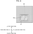
- Fig. 4 is a plan view of one of the pixels 20 in Fig. 3A , as viewed from an upper layer (entrance surface side).
- a region outside the photodiode 201 is shielded from light by a light shielding portion 401 of the pixel 20.
- the photodiode 201 is provided with an aperture on the upper side thereof (see also Fig. 5A ) where the light shielding portion 401 is absent.
- a long side of the aperture is parallel to the long side of the exit plane 302a, and a short side of the aperture is parallel to the short side of the exit plane 302a.
- a component capable of blocking light such as a tungsten member, may be used as the light shielding portion 401.
- Figs. 5A and 5B each illustrate a cross-sectional structure of one of the pixels 20 illustrated in Fig. 3A .
- Fig. 5A is a cross-sectional view taken along line VA-VA of Fig. 3A .
- the photodiode 201 and the capacitive element 202 are formed in the semiconductor substrate 600.
- the capacitive element 202 and the first transfer transistor 204 are shielded from light by the light shielding portion 401.
- An interlayer insulating layer (not shown) is formed between adjacent ones of a line 402, a line 403, and a line 404.
- a silicon dioxide (SiO) film with a refractive index of about 1.5 is used as the interlayer insulating layer.
- the light guiding path 302 is disposed above the photodiode 201.
- the light guiding path 302 has the entrance surface 302y and the exit surface 302x.
- the pixel 20 further includes a color filter 500, a microlens 501, and an interlayer lens 502. Light transmitted through the microlens 501, the color filter 500, and the interlayer lens 502 enters the entrance surface 302y.
- the length of the exit surface 302x in the first direction is the length Len_b.
- Fig. 5B is a cross-sectional view taken along line VB-VB of Fig. 3A .
- the length of the exit surface 302x in the second direction is the length Len_a.
- the length Len_b is shorter than the length Len_a.
- a silicon oxynitride (SiON) film with a refractive index of about 1.8 is used as the light guiding path 302.
- Light originating from the inside of the light guiding path 302 and entering the interface between the light guiding path 302 and the interlayer insulating layer at a predetermined angle is entirely reflected back to the inside of the light guiding path 302.
- the light guiding path 302 can thus guide light entering the entrance surface 302y to the exit surface 302x while reducing leakage of light to the interlayer insulating layer.
- the amount of light entering the photodiode 201 is larger than that in the case without the light guiding path 302. This means that with the light guiding path 302, the sensitivity of the photodiode 201 is greater than that in the case without the light guiding path 302.
- the imaging device of the present embodiment is developed, which takes into account the layout of the light guiding path 302 and the capacitive element 202.
- the capacitive element 202 is disposed such that the center of gravity thereof is located in a region between a first line and a second line both extending from the center of gravity of the exit plane 302a.
- the first line divides the angle between the first direction and the second direction into two equal parts
- the second line divides the angle between a third direction opposite the second direction and the first direction into two equal parts.
- a first line LZ1 is a bisector that extends from a center of gravity Z1 of the exit plane 302a in plan view and divides the angle between the first direction and the second direction into two equal parts.
- a second line LZ2 is a bisector that also extends from the center of gravity Z1 of the exit plane 302a in plan view and divides the angle between the third direction opposite the second direction and the first direction into two equal parts.
- a center of gravity Z2 of the capacitive element 202 is located in the region between the first line LZ1 and the second line LZ2.
- the capacitive element 202 is disposed closer to a long side 310 than to a short side 315 of the exit plane 302a, which is obtained by projecting the exit surface 302x of the light guiding path 302 onto the semiconductor substrate 600. More specifically, the capacitive element 202 is disposed between the long side 310 of the exit plane 302a and the element isolation region 400 formed between the long side 310 and the pixel 20 adjacent thereto in the first direction.
- the long sides 310 of the exit plane 302a have a length extending in the second direction and longer than the short sides 315 of the exit plane 302a.
- a method of defining the length of each side of the exit surface 302x when the exit surface 302x is not rectangular will be described.
- a first side of the exit surface 302x (exit plane 302a) and a second side of the exit surface 302x extending in a direction intersecting the first side are both extended beyond the corresponding corner having a curvature.
- a third side and a fourth side extending in a direction intersecting the third side are both extended beyond the corresponding corner having a curvature. The distance between two adjacent points of intersection can thus be treated as the length of each side.
- the photodiode 201 of a first pixel and the photodiode 201 of a second pixel are arranged along the first direction.
- the capacitive element 202 of the first pixel is disposed between the photodiode 201 of the first pixel and the photodiode 201 of the second pixel.
- the exit surface 302x of the light guiding path 302 of the first pixel is larger in length Len_a in the second direction orthogonal to the first direction in plan view than in length Len_b in the first direction.
- the second direction may not coincide with the direction of the long sides of the exit surface 302x.
- the largest length of the exit surface 302x in the second direction can be defined as the length of the long sides.
- the first direction may not coincide with the direction of the short sides of the exit surface 302x.
- the largest length of the exit surface 302x in the first direction can be defined as the length of the short sides.
- Figs. 6A and 6B are plan views each illustrating a layout of the photodiode 201, the capacitive element 202, and the exit plane 302a.
- Fig. 6A illustrates an example in which, as in Fig. 3A , the center of gravity Z2 of the capacitive element 202 is located in the region between the first line LZ1 and the second line LZ2.
- Fig. 6B illustrates an example in which the center of gravity Z2 of the capacitive element 202 is not located in the region between the first line LZ1 and the second line LZ2.
- Fig. 6A illustrates an example in which the capacitive element 202 is disposed between the element isolation region 400 formed between the pixels 20 adjacent in the first direction and the long side 310.
- Fig. 6B illustrates an example in which the capacitive element 202 is disposed between the element isolation region 400 formed between the pixels 20 adjacent in the second direction and the short side 315.
- the distance between the capacitive element 202 and the exit plane 302a is denoted as distance A.
- the distance between the capacitive element 202 and the exit plane 302a is denoted as distance B.
- the distance A is larger than the distance B.
- the capacitive element 202 is disposed such that the center of gravity Z2 thereof is located in the region between the first line LZ1 and the second line LZ2.
- the capacitive element 202 can be disposed farther from the exit surface 302x of the light guiding path 302.
- the capacitive element 202 when the capacitive element 202 is disposed between the element isolation region 400 formed between the pixels 20 adjacent in the first direction and the long side 310, the capacitive element 202 can be made farther from the exit surface 302x of the light guiding path 302 than in the layout illustrated in Fig. 6B .
- the pixels 20 are arranged along both the first and second directions of the exit plane 302a in the present embodiment, the arrangement of the pixels 20 is not limited to this.
- the pixels 20 may be arranged along any directions which include a direction corresponding to the first direction and a direction corresponding to the second direction.
- a direction corresponding to the first direction is a direction closer to the first direction than to the second direction, and typically forms an angle within a range of plus or minus 10 degrees from the first direction.
- the capacitive element 202 is not limited to that of the present embodiment.
- the capacitive element 202 may be a polysilicon-insulator-polysilicon (PiP) capacitor formed by a plurality of polysilicon layers with an insulating layer therebetween.
- SiP polysilicon-insulator-polysilicon
- An imaging device according to a second embodiment will be described mainly about differences from the first embodiment.
- Fig. 7A illustrates an example where the exit plane 302a described with reference to Fig. 3A is in the shape of a hexagon, which is an example of a polygon.
- Fig. 7B illustrates an example where the exit plane 302a is in the shape of an ellipse.
- the entrance plane 302b is geometrically similar to, and greater in size than, the exit plane 302a.
- the length Len_a represents the length of the longest of the diagonals each connecting two nonadjacent vertices of the hexagon
- the length Len_b represents the length of the diagonals orthogonal to the longest diagonals of the hexagon.
- the length Len_b is shorter than the length Len_a.
- the center of gravity Z2 of the capacitive element 202 is also located in the region between the first line LZ1 and the second line LZ2.
- the capacitive element 202 is disposed between the longest diagonal of the exit plane 302a extending in the second direction and the element isolation region 400 (see the first embodiment) extending in a direction corresponding to the second direction.
- the photodiode 201 of the first pixel and the photodiode 201 of the second pixel are arranged along the first direction.
- the capacitive element 202 of the first pixel is disposed between the photodiode 201 of the first pixel and the photodiode 201 of the second pixel.
- the length of the longest diagonals in the second direction is longer than the length of the diagonals in the first direction orthogonal to the longest diagonals.
- the second direction may not coincide with the direction of the diagonals of the exit surface 302x.
- the largest length of the exit surface 302x in the second direction can be defined as the length of the diagonals.
- the first direction may not coincide with the direction of the diagonals of the exit surface 302x.
- the largest length of the exit surface 302x in the first direction can be defined as the length of the diagonals.
- the length Len_a and the length Len_b represent the lengths of the major axis and the minor axis, respectively, of the exit plane 302a having an elliptical shape.
- the length Len_b is shorter than the length Len_a.
- the center of gravity Z2 of the capacitive element 202 is also located in the region between the first line LZ1 and the second line LZ2.
- the capacitive element 202 is disposed between the major axis of the exit plane 302a extending in the second direction and the element isolation region 400 (see the first embodiment) extending in a direction corresponding to the second direction.
- the photodiode 201 of the first pixel and the photodiode 201 of the second pixel are arranged along the first direction.
- the capacitive element 202 of the first pixel is disposed between the photodiode 201 of the first pixel and the photodiode 201 of the second pixel.
- the length of the major axis in the second direction orthogonal to the first direction in plan view is longer than the length of the minor axis in the first direction.
- the second direction may not coincide with the direction of the major axis of the exit surface 302x.
- the largest length of the exit surface 302x in the second direction can be defined as the length of the exit surface 302x in the second direction.
- the first direction may not coincide with the direction of the minor axis of the exit surface 302x.
- the largest length of the exit surface 302x in the first direction can be defined as the length of the exit surface 302x in the first direction.
- An imaging device according to a third embodiment will be described mainly about differences from the second embodiment.
- the entrance plane 302b is geometrically similar to the exit plane 302a. In the imaging device of the present embodiment, the entrance plane 302b and the exit plane 302a are not geometrically similar.
- Fig. 8A illustrates an example where the entrance plane 302b is square in shape and the exit plane 302a is rectangular in shape.
- Fig. 8B is a cross-sectional view taken along line VIIIB-VIIIB of Fig. 8A and shows a plane parallel to the x direction (second direction).
- Fig. 8C is a cross-sectional view taken along line VIIIC-VIIIC of Fig. 8A and shows a plane parallel to the y direction (first direction).
- a comparison between Figs. 8B and 8C shows that the taper angle of the light guiding path 302 in Fig. 8B is steeper than that in Fig. 8C . That is, the taper angle of the light guiding path 302 in the plane parallel to the second direction is steeper than the taper angle of the light guiding path 302 in the plane parallel to the first direction.
- the leakage of light from the side face of the light guiding path 302 into the interlayer insulating layer is reduced as the taper angle becomes steeper.
- the imaging device of the present embodiment is configured such that the taper angle of the light guiding path 302 is steeper on the side with the capacitive element 202 than that on the side without the capacitive element 202.
- the entry of light from the side face of the light guiding path 302 into the capacitive element 202 can be made less than that in the case where the entrance plane 302b is geometrically similar to the exit plane 302a.
- Fig. 8D illustrates the entrance plane 302b having a regular polygonal shape and the exit plane 302a having a polygonal shape.
- Fig. 8E illustrates the entrance plane 302b having a perfect circular shape and the exit plane 302a having an elliptical shape.
- the taper angle of the light guiding path 302 is steeper on the side with the capacitive element 202 than that on the side without the capacitive element 202.
- the entry of light from the side face of the light guiding path 302 into the capacitive element 202 can be made less than that in the case where the entrance plane 302b is geometrically similar to the exit plane 302a.
- Fig. 9 is a circuit diagram of the pixels 20 of an imaging device according to a fourth embodiment.
- the pixels 20 of the imaging device according to the present embodiment each include a capacitive element 202-1 connected through a transistor 204-1 to the photodiode 201, and a capacitive element 202-2 connected through a transistor 204-2 to the photodiode 201.
- the capacitive element 202-1 is connected through a transistor 205-1 to the FD portion 203.
- the capacitive element 202-2 is connected through a transistor 205-2 to the FD portion 203.
- a transistor 250 is connected to the FD portion 203.
- the transistor 250 is turned on.
- a combined capacitor formed by the capacitance of the transistor 250 and the capacitance of the FD portion 203 is connected to the amplifying transistor 210. That is, the capacitor connected to the amplifying transistor 210 can be changed by turning on and off the transistor 250.
- each pixel 20 of the present embodiment can change a charge-to-voltage conversion coefficient used to convert electric charges transferred to the FD portion 203 into a gate voltage of the amplifying transistor 210.
- Figs. 10A and 10B each illustrate a layout of the capacitive element 202-1, the capacitive element 202-2, and the exit plane 302a. Reference numerals shown in Figs. 10A and 10B correspond to those in Fig. 9 .
- the capacitive element 202-1 and the capacitive element 202-2 are arranged along the second direction.
- a center of gravity Z2-1 of the capacitive element 202-1 and a center of gravity Z2-2 of the capacitive element 202-2 are both located in the region between the first line LZ1 and the second line LZ2.
- the capacitive element 202-1 and the capacitive element 202-2 are disposed between the long side 310 of the exit plane 302a extending in the second direction and the element isolation region 400 (see the first embodiment) extending in a direction corresponding to the second direction.
- the imaging device that includes the pixel 20 of Fig. 10A , including the two capacitive elements 202-1 and 202-2, can also achieve both improved sensitivity and reduced degradation of image quality.
- the capacitive element 202-1 and the capacitive element 202-2 are arranged along the first direction.
- the center of gravity Z2-1 of the capacitive element 202-1 is located in the region between the first line LZ1 and the second line LZ2.
- a third line LZ3 is a bisector that divides the angle between a fourth direction opposite the first direction and the third direction opposite the second direction into two equal parts.
- a fourth line LZ4 is a bisector that divides the angle between the fourth direction opposite the first direction and the second direction into two equal parts.
- the center of gravity Z2-2 of the capacitive element 202-2 is located in the region between the third line LZ3 and the fourth line LZ4.
- the capacitive element 202-1 is disposed between the element isolation region 400 (see the first embodiment) formed between the pixels 20 adjacent in the first direction and extending in a direction corresponding to the second direction, and a long side 310-1 of the exit plane 302a extending in the second direction.
- the capacitive element 202-2 is disposed between the element isolation region 400 (see the first embodiment) formed between the pixels 20 adjacent in the fourth direction and extending in a direction corresponding to the second direction, and a long side 310-2 of the exit plane 302a extending in the second direction.
- the long side 310-1 and the long side 310-2 are opposite sides.
- the pixels 20 each including the light guiding path 302 of the present embodiment can also be two-dimensionally arranged as illustrated in Fig. 3A .
- the photodiode 201 of the first pixel and the photodiode 201 of the second pixel are arranged along the first direction.
- the capacitive element 202-1 and the capacitive element 202-2 of the first pixel are disposed between the photodiode 201 of the first pixel and the photodiode 201 of the second pixel.
- the photodiode 201 of the first pixel and the photodiode 201 of a third pixel are arranged along the fourth direction opposite the first direction.
- the capacitive element 202-2 of the first pixel is disposed between the photodiode 201 of the first pixel and the photodiode 201 of the third pixel.
- the capacitive element 202-1 of the first pixel is disposed between the photodiode 201 of the first pixel and the photodiode 201 of the second pixel.
- the imaging device that includes the pixel 20 of Fig. 10B , including the two capacitive elements 202-1 and 202-2, can also achieve both improved sensitivity and reduced degradation of image quality.
- the imaging device of the present embodiment includes the capacitive element 202-1 and the capacitive element 202-2.
- the imaging device is capable of performing an operation in which electric charges accumulated by the photodiode 201 during a charge accumulation period for an n-th frame are retained by the capacitive element 202-1, and electric charges accumulated by the photodiode 201 during a charge accumulation period for an (n+1)-th frame are retained by the capacitive element 202-2.
- the electric charges accumulated in the (n+1)-th frame by the photodiode 201 can be output to the capacitive element 202-2.
- the photodiode 201 can generate electric charges while transferring the electric charges to the capacitive element 202-2. This allows electric charges exceeding the saturation capacitance of the photodiode 201 to be retained in the capacitive element 202-2.
- Electric charges accumulated by the photodiode 201 during the charge accumulation period for the (n+1)-th frame can be retained in the capacitive element 202-2 by repeating the transfer of electric charges from the photodiode 201 to the capacitive element 202-2.
- This transfer operation can be repeated by repeatedly causing the signal pTX2 to transition from non-active level to active level, and then to non-active level in sequence.
- high-luminance light which is saturated in the case of accumulation of electric charges in the photodiode 201 alone, enters the photodiode 201, electric charges corresponding to the luminance can be retained in the capacitive element 202-2.
- the signal pTX1 may also be caused to transition from non-active level to active level, and then to non-active level in sequence. Thus, electric charges exceeding the saturation capacitance of the photodiode 201 can also be retained in the capacitive element 202-1.
- each pixel includes a plurality of photodiodes.
- the plurality of photodiodes are arranged to allow entry of light transmitted through one microlens. Light transmitted through regions with different exit pupils enters the plurality of photodiodes.
- a phase difference is detected from a signal based on electric charges generated by one of the plurality of photodiodes and a signal based on electric charges generated by another of the plurality of photodiodes.
- an autofocus operation can be performed, in which the focus of an optical system that causes light to enter the imaging device is adjusted to the subject.
- Fig. 11 is a circuit diagram of pixels 20-2 of the present embodiment.
- the pixels 20-2 each include a photodiode 201-1 and a photodiode 201-2.
- the photodiode 201-1 and the photodiode 201-2 are arranged to allow entry of light transmitted through one microlens.
- a transfer transistor 204-3 and a PD reset transistor 206-1 are connected to the photodiode 201-1.
- a capacitive element 202-3 is connected through the transfer transistor 204-3 to the photodiode 201-1.
- the capacitive element 202-3 is connected through a transfer transistor 205-3 to the FD portion 203.
- a transfer transistor 204-4 and a PD reset transistor 206-2 are connected to the photodiode 201-2.
- a capacitive element 202-4 is connected through the transfer transistor 204-4 to the photodiode 201-2.
- the capacitive element 202-4 is connected through a transfer transistor 205-4 to the FD portion 203.
- Fig. 12 illustrates a layout of the photodiode 201-1, the photodiode 201-2, the transfer transistor 204-3, the transfer transistor 204-4, the capacitive element 202-3, the capacitive element 202-4, and the exit plane 302a of the pixel 20-2 illustrated in Fig. 11 .
- a center of gravity Z2-3 of the capacitive element 202-3 and a center of gravity Z2-4 of the capacitive element 202-4 are located in the region between the first line LZ1 and the second line LZ2 both extending from the center of gravity Z1 of the exit plane 302a.
- the capacitive element 202-3 and the capacitive element 202-4 are disposed between the long side 310 of the exit plane 302a and the element isolation region 400 (see the first embodiment) extending in a direction corresponding to the second direction.
- the imaging device of the present embodiment can achieve both improved sensitivity and reduced degradation of image quality.
- a plurality of photodiodes are provided for one microlens.
- the imaging device of the present embodiment thus can perform an autofocus operation which involves detecting a phase difference.
- An imaging device of the present embodiment also includes pixels each including a plurality of photodiodes for one microlens.
- the pixel of the imaging device according to the present embodiment differs from that of the imaging device of the fifth embodiment in that a plurality of capacitive elements are connected to each of the plurality of photodiodes.
- Fig. 13 is a circuit diagram of pixels of the imaging device according to the present embodiment.
- Each pixel 20-3 includes a photodiode 201-3 and a photodiode 201-4.
- the photodiode 201-3 and the photodiode 201-4 are arranged to allow entry of light transmitted through one microlens. Light transmitted through regions with different exit pupils enters the photodiode 201-3 and the photodiode 201-4.
- a phase difference is detected from a signal based on electric charges generated by one of the photodiode 201-3 and the photodiode 201-4 and a signal based on electric charges generated by the other of the photodiode 201-3 and the photodiode 201-4.
- an autofocus operation can be performed, in which the focus of the optical system that causes light to enter the imaging device is adjusted to the subject.
- the photodiode 201-3 is connected through a transfer transistor 204-5 to a capacitive element 202-5.
- the photodiode 201-3 is connected through a transfer transistor 204-6 to a capacitive element 202-6.
- the photodiode 201-3 is connected to a PD reset transistor 206-3.
- the capacitive element 202-5 is connected through a transfer transistor 205-5 to an FD portion 203-1.
- the capacitive element 202-6 is connected through a transfer transistor 205-6 to the FD portion 203-1.
- the FD portion 203-1 is connected to the gate of an amplifying transistor 210-1.
- the amplifying transistor 210-1 is connected through a selecting transistor 207-1 to a column signal line 10-1.
- the photodiode 201-4 is connected through a transfer transistor 204-7 to a capacitive element 202-7.
- the photodiode 201-4 is connected through a transfer transistor 204-8 to a capacitive element 202-8.
- the photodiode 201-4 is connected to a PD reset transistor 206-4.
- the capacitive element 202-7 is connected through a transfer transistor 205-7 to an FD portion 203-2.
- the capacitive element 202-8 is connected through a transfer transistor 205-8 to the FD portion 203-2.
- the FD portion 203-2 is connected to the gate of an amplifying transistor 210-2.
- the amplifying transistor 210-2 is connected through a selecting transistor 207-2 to a column signal line 10-2.
- Figs. 14A and 14B each illustrate a layout of the photodiodes 201-3 and 201-4, the transfer transistors 204-5, 204-6, 204-7 and 204-8, the capacitive elements 202-5, 202-6, 202-7, and 202-8, and the exit plane 302a of the pixel 20-3 illustrated in Fig. 13 .
- Reference numerals shown in Figs. 14A and 14B correspond to those in Fig. 13 .
- the pixel 20-3 illustrated in Fig. 14A includes the photodiodes 201-3 and 201-4 having a rectangular shape.
- a center of gravity Z2-5 of the capacitive element 202-5 and a center of gravity Z2-6 of the capacitive element 202-7 are located in the region between the first line LZ1 and the second line LZ2 both extending from the center of gravity Z1 of the exit plane 302a.
- a center of gravity Z2-7 of the capacitive element 202-6 and a center of gravity Z2-8 of the capacitive element 202-8 are located in the region between the third line LZ3 and the fourth line LZ4 both extending from the center of gravity Z1 of the exit plane 302a.
- the third line LZ3 is a bisector that divides the angle between the third direction and the fourth direction into two equal parts.
- the fourth line LZ4 is a bisector that divides the angle between the second direction and the fourth direction into two equal parts.
- the capacitive element 202-5 and the capacitive element 202-7 are disposed between the element isolation region 400 (see the first embodiment) formed between the pixels 20-3 adjacent in the first direction and extending in a direction corresponding to the second direction, and the long side 310-1 of the exit plane 302a.
- the capacitive element 202-6 and the capacitive element 202-8 are disposed between the element isolation region 400 formed between the pixels 20-3 adjacent in the fourth direction and extending in a direction corresponding to the second direction, and the long side 310-2 of the exit plane 302a.
- Fig. 14B illustrates another layout of one of the pixels 20-3 illustrated in Fig. 13 .
- the capacitive elements 202-5, 202-6, 202-7, and 202-8 each include a portion extending in the second direction and another portion extending therefrom in the first or fourth direction.
- the center of gravity Z2-5 of the capacitive element 202-5 and the center of gravity Z2-6 of the capacitive element 202-7 are located in the region between the first line LZ1 and the second line LZ2.
- the center of gravity Z2-7 of the capacitive element 202-6 and the center of gravity Z2-8 of the capacitive element 202-8 are located in the region between the third line LZ3 and the fourth line LZ4.
- the capacitive element 202-5 and the capacitive element 202-7 are disposed between the element isolation region 400 (see the first embodiment) formed between the pixels 20-3 adjacent in the first direction and extending in a direction corresponding to the second direction, and the long side 310-1 of the exit plane 302a.
- the capacitive element 202-6 and the capacitive element 202-8 are disposed between the element isolation region 400 formed between the pixels 20-3 adjacent in the fourth direction and extending in a direction corresponding to the second direction, and the long side 310-2 of the exit plane 302a.
- the pixels 20-3 each including the light guiding path 302 of the present embodiment can also be two-dimensionally arranged as illustrated in Fig. 3A .
- the pair of photodiodes 201-3 and 201-4 of the first pixel and the pair of photodiodes 201-3 and 201-4 of the second pixel are arranged along the first direction.
- the capacitive elements 202-5 and 202-7 of the first pixel are disposed between the pair of photodiodes 201-3 and 201-4 of the first pixel and the pair of photodiodes 201-3 and 201-4 of the second pixel.
- the pair of photodiodes 201-3 and 201-4 of the first pixel and the pair of photodiodes 201-3 and 201-4 of the third pixel are arranged along the fourth direction opposite the first direction.
- the capacitive elements 202-6 and 202-8 of the first pixel are disposed between the pair of photodiodes 201-3 and 201-4 of the first pixel and the pair of photodiodes 201-3 and 201-4 of the third pixel.
- the imaging device of the present embodiment can also achieve both improved sensitivity and reduced degradation of image quality.
- FIG. 15 is a block diagram of a digital still camera serving as an example of the imaging system.
- the present embodiment relates to an imaging system that includes, in the form of an imaging device 1504, the imaging device according to any of the embodiments described above.
- the imaging system illustrated in Fig. 15 includes a barrier 1501 for lens protection, a lens 1502 that forms an optical image of a subject on the imaging device 1504, and an aperture 1503 for varying the amount of light passing through the lens 1502.
- the lens 1502 and the aperture 1503 form an optical system that concentrates light onto the imaging device 1504.
- the imaging system illustrated in Fig. 15 further includes an output signal processing unit 1505 that processes output signals from the imaging device 1504.
- the output signal processing unit 1505 performs various types of correction and compression as necessary, and outputs signals. Also, the output signal processing unit 1505 generates an image using signals output from the imaging device 1504.
- the imaging system illustrated in Fig. 15 further includes a buffer memory unit 1506 for temporarily storing image data, and an external interface (I/F) unit 1507 for communicating with an external computer and the like.
- the imaging system further includes a removable recording medium 1509, such as a semiconductor memory, for recording or reading captured image data, and a recording-medium control interface (I/F) unit 1508 for recording data on or reading data from the recording medium 1509.
- the imaging system further includes an overall control/computing unit 1510 that controls various computations and an overall operation of the digital still camera, and a timing generator 1511 that outputs various timing signals to the imaging device 1504 and the output signal processing unit 1505.
- the timing signals and the like may be input from the outside.
- the imaging system may have any configuration as long as it includes at least the imaging device 1504 and the output signal processing unit 1505 that processes output signals from the imaging device 1504.
- the pixels 20 may each include a plurality of photodiodes for one microlens.
- the output signal processing unit 1505 processes a signal based on electric charges generated by one of the photodiodes of the pixel 20 and a signal based on electric charges generated by the other photodiode of the pixel 20.
- the output signal processing unit 1505 can thus acquire distance information about the distance from the imaging device 1504 to the subject.
- the pixels 20 may each include more photoelectric converters for one microlens. That is, the output signal processing unit 1505 uses a signal based on electric charges generated by a part of a plurality of photoelectric converters (ex.
- the output signal processing unit 1505 may be configured to acquire distance information about the distance from the imaging device 1504 to the subject using these two signals.
- the signal based on electric charges generated by the another part of the plurality of photoelectric converters may be obtained by subtracting the signal based on electric charges generated by the part of the photoelectric converters from a signal based on the sum of electric charges generated by the plurality of photoelectric converters.
- the output signal processing unit 1505 is disposed on a second semiconductor substrate different from a first semiconductor substrate having the imaging device 1504 thereon.
- the first semiconductor substrate and the second semiconductor substrate may be provided as separate chips, or may be stacked together to form a single chip.
- the imaging system of the present embodiment is capable of performing an imaging operation using the imaging device 1504.
- FIG. 16A illustrates an imaging system related to a vehicle-mounted camera.
- An imaging system 1000 is an imaging system that includes, in the form of an imaging device 1010, the imaging device according to any of the embodiments described above.
- the imaging system 1000 includes an image processing unit 1030 that performs image processing on a plurality of pieces of image data acquired by the imaging device 1010, and a parallax acquiring unit 1040 that acquires a parallax (i.e., a phase difference between parallax images) from the plurality of pieces of image data acquired by the imaging system 1000.
- a parallax i.e., a phase difference between parallax images
- the parallax may be acquired using signals output from the plurality of imaging devices 1010.
- the imaging system 1000 may include the imaging device 1010 that includes a plurality of photoelectric converters for one microlens.
- the parallax acquiring unit 1040 acquires a parallax by processing a signal based on electric charges generated by a part of the plurality of photoelectric converters and a signal based on electric charges generated by another part of the plurality of photoelectric converters.
- the parallax acquiring unit 1040 may acquire a parallax using a signal based on electric charges generated by the part of the plurality of photoelectric converters corresponding to one microlens and a signal based on electric charges generated by the another part of the plurality of photoelectric converters.
- the signal based on electric charges generated by the another part of the plurality of photoelectric converters may be obtained by subtracting the signal based on electric charges generated by the part of the plurality of photoelectric converters from a signal based on the sum of electric charges generated by the plurality of photoelectric converters.
- the imaging system 1000 includes a distance acquiring unit 1050 that acquires a distance to an object on the basis of the acquired parallax, and a collision determination unit 1060 that determines the possibility of collision on the basis of the acquired distance.
- the parallax acquiring unit 1040 and the distance acquiring unit 1050 are examples of a distance information acquiring unit that acquires distance information about a distance to the object. That is, the distance information is information about a parallax, the amount of defocusing, a distance to the object, and the like.
- the collision determination unit 1060 may determine the possibility of collision using any of the distance information described above.
- the distance information acquiring unit may be implemented by specifically-designed hardware, a software module, or a combination of both.
- the distance information acquiring unit may be implemented by a field programmable gate array (FPGA), an application specific integrated circuit (ASIC), or a combination of both.
- FPGA field programmable gate array
- ASIC application specific integrated circuit
- the imaging system 1000 is connected to a vehicle information acquiring device 1310 and can acquire vehicle information, such as a vehicle speed, a yaw rate, and a rudder angle.
- the imaging system 1000 is also connected to a control ECU 1410 which is a control unit that outputs a control signal for generating a braking force to a vehicle on the basis of the determination made by the collision determination unit 1060.
- the imaging system 1000 is also connected to an alarm device 1420 that gives an alarm to a vehicle driver on the basis of the determination made by the collision determination unit 1060. For example, if the collision determination unit 1060 determines that a collision is highly likely, the control ECU 1410 performs vehicle control to avoid the collision or reduce damage by applying the brake, releasing the accelerator, or suppressing the engine output.
- the alarm device 1420 gives an alarm to the user, for example, by sounding an audio alarm, displaying alarm information on the screen of a car navigation system, or vibrating the seatbelt or steering wheel.
- the imaging system 1000 captures an image of the surroundings of the vehicle, such as the front or rear of the vehicle.
- Fig. 16B illustrates the imaging system 1000 that is operating to capture an image of the front of the vehicle.
- a control operation for avoiding a collision with other vehicles has been described, the same configuration is also applicable to a self-driving control operation for following other vehicles, and to a self-driving control operation for not driving out of the lane.
- the imaging system described above is applicable not only to vehicles, such as those having the imaging system mounted thereon, but also to moving bodies (moving devices), such as ships, aircrafts, and industrial robots.
- the imaging system is applicable not only to moving bodies, but is also widely applicable to devices using an object recognition technique, such as intelligent transport systems (ITSs).
- ITSs intelligent transport systems
Abstract
Description
- The present invention relates to an imaging device and an imaging system.
- An imaging device, such as that disclosed in Japanese Patent Laid-Open No.
2015-228468 2015-228468 - Japanese Patent Laid-Open No.
2015-228468 2015-228468 - The present invention has been made in view of the problem described above.
- The present invention in its first aspect provides an imaging device as specified in
claims 1 to 7. - The present invention in its second aspect provides an imaging device as specified in claims 8 to 16.
- The present invention in its third aspect provides an imaging system as specified in claim 17.
- The present invention in its fourth aspect provides an imaging system as specified in claim 18.
- The present invention in its fifth aspect provides a moving body as specified in claim 19.
- Further features of the present invention will become apparent from the following description of exemplary embodiments with reference to the attached drawings. Each of the embodiments of the present invention described below can be implemented solely or as a combination of a plurality of the embodiments. Also, features from different embodiments can be combined where necessary or where the combination of elements or features from individual embodiments in a single embodiment is beneficial.
-
-
Fig. 1 illustrates a configuration of an imaging device according to a first embodiment. -
Fig. 2 illustrates a circuit configuration of pixels according to the first embodiment. -
Fig. 3A is a plan view of a layout of some of the pixels illustrated inFigs. 1 and2 , andFig. 3B illustrates dimensions of an exit plane of one of the pixels illustrated inFig. 3A . -
Fig. 4 is a plan view of a layout of one of the pixels illustrated inFig. 3A . -
Figs. 5A and 5B each illustrate a cross-sectional structure of one of the pixels illustrated inFig. 3A . -
Figs. 6A and 6B are plan views each illustrating a layout of a pixel. -
Figs. 7A and 7B are plan views each illustrating a layout of a pixel according to a second embodiment. -
Figs. 8A, 8D, and 8E are plan views each illustrating a layout of part of a pixel according to a third embodiment, andFigs. 8B and 8C are cross-sectional views ofFig. 8A . -
Fig. 9 illustrates a circuit configuration of pixels according to a fourth embodiment. -
Figs. 10A and 10B are plan views each illustrating a layout of a pixel according to the fourth embodiment. -
Fig. 11 illustrates a circuit configuration of pixels according to a fifth embodiment. -
Fig. 12 is a plan view illustrating a layout of a pixel according to the fifth embodiment. -
Fig. 13 illustrates a circuit configuration of pixels according to a sixth embodiment. -
Figs. 14A and 14B are plan views each illustrating a layout of a pixel according to the sixth embodiment. -
Fig. 15 illustrates a configuration of an imaging system according to a seventh embodiment. -
Figs. 16A and 16B illustrate a configuration of an imaging system according to an eighth embodiment. - Hereinafter, an imaging device according to embodiments of the present invention will be described, which is configured to sufficiently reduce the entry of light from a light guiding path into a charge accumulation portion.
- Throughout the drawings, the same components are denoted by the same reference numerals. A redundant description of components may be omitted. The embodiments described below are for illustrative purposes, and the present invention is not limited to the embodiments described below.
-
Fig. 1 illustrates an imaging device according to a first embodiment. The imaging device of the present embodiment includescolumn signal lines 10 andpixels 20. In apixel array 100, thepixels 20 are arranged in a plurality of rows and columns. Thecolumn signal lines 10 are arranged to correspond to the respective columns of thepixels 20. The imaging device further includes avertical scanning circuit 101. Thepixels 20 are connected row-by-row to thecolumn signal lines 10 throughcontrol lines 30 such that a common signal is supplied from thevertical scanning circuit 101 to each row ofpixels 20. Thevertical scanning circuit 101 is a control unit that controls the accumulation period of thepixels 20. - The imaging device further includes a
column circuit unit 102, ahorizontal scanning circuit 103, and anoutput circuit 104. Thecolumn circuit unit 102 includes a plurality of column circuits, each of which corresponds to one of the plurality ofcolumn signal lines 10. The plurality of column circuits are each configured to output, to theoutput circuit 104, a signal obtained by amplifying a signal output to the correspondingcolumn signal line 10. - The
horizontal scanning circuit 103 is configured to sequentially select the plurality of column circuits of thecolumn circuit unit 102. This causes the signals retained by the plurality of column circuits to be sequentially output to theoutput circuit 104. Theoutput circuit 104 is configured to output signals to the outside of the imaging device. The signals output by theoutput circuit 104 are those output by the imaging device. - The imaging device further includes a
control circuit 105. Thecontrol circuit 105 is connected to each of thevertical scanning circuit 101, thecolumn circuit unit 102, and thehorizontal scanning circuit 103 through a drive line for supplying a drive signal. -
Fig. 2 illustrates a configuration of thepixels 20 in detail. - The
pixels 20 each include aphotodiode 201. Thephotodiode 201 is a photoelectric converter that generates a signal corresponding to incident light. Thepixel 20 further includes afirst transfer transistor 204 and asecond transfer transistor 205. Thepixel 20 further includes acapacitive element 202 and a floating diffusion (FD)portion 203. Thecapacitive element 202 is a charge accumulation portion that retains signals accumulated by thephotodiode 201. Thecapacitive element 202, which serves as a charge accumulation portion, is electrically connected through thefirst transfer transistor 204 to thephotodiode 201, which serves as a photoelectric converter. TheFD portion 203 is electrically connected through thesecond transfer transistor 205 to thecapacitive element 202, which serves as a charge accumulation portion. - The
pixel 20 further includes areset transistor 209, which is supplied with a source voltage from avoltage source 211. Thereset transistor 209 is electrically connected to theFD portion 203. - The
pixel 20 further includes an amplifyingtransistor 210 and a selectingtransistor 207. TheFD portion 203 is connected to the input node of the amplifyingtransistor 210. - The amplifying
transistor 210 is supplied with a source voltage from thevoltage source 211. The amplifyingtransistor 210 is electrically connected through the selectingtransistor 207 to the correspondingcolumn signal line 10. - A current source (not shown) is electrically connected to the
column signal line 10. When the selectingtransistor 207 is in the ON state, the amplifyingtransistor 210 forms a source follower circuit with the source voltage supplied from thevoltage source 211 and the current source electrically connected to thecolumn signal line 10. InFig. 2 , a signal output to a corresponding one of thecolumn signal lines 10 is denoted as signal Vout(p). Note that (p) at the end indicates a column number. - The
pixel 20 further includes aPD reset transistor 206, which is supplied with a source voltage from thevoltage source 211. - As illustrated in
Fig. 1 , thepixels 20 and thevertical scanning circuit 101 are electrically connected through the control lines 30. A signal pTX1(m) is input to the gate of thefirst transfer transistor 204. Hereinafter, (m) at the end indicates that the signal is input to thepixels 20 in the m-th row. Signals input to a plurality of rows ofpixels 20 are collectively denoted without (m). - A signal pTX2(m) is input to the gate of the
second transfer transistor 205. - A signal pOFG(m) is input to the gate of the PD reset
transistor 206. - The signals pTX1 input to the plurality of rows of
pixels 20 are brought to the active level at the same time, and brought to the non-active level at the same time. The signals pOFG input to the plurality of rows ofpixels 20 are brought to the active level at the same time, and brought to the non-active level at the same time. The imaging device of the present embodiment thus performs a global electronic shutter operation in which thephotodiodes 201 of all thepixels 20 start signal accumulation at the same time and end the signal accumulation at the same time. - A signal pRES(m) is input to the gate of the
reset transistor 209. - A signal pSEL(m) is input to the gate of the selecting
transistor 207. -
Fig. 3A is a top view of some of thepixels 20 described with reference toFigs. 1 and2 .Fig. 3A illustrates three rows by two columns ofpixels 20. - Reference numerals in
Fig. 3A correspond to those shown inFig. 2 . Anexit plane 302a is a plane obtained by projecting, onto a semiconductor substrate 600 (seeFig. 5A ) having thephotodiode 201 therein, anexit surface 302x of alight guiding path 302 that guides light to thephotodiode 201. Theexit plane 302a can be regarded as being rectangular in shape. Similarly, anentrance plane 302b is a plane obtained by projecting, onto thesemiconductor substrate 600 having thephotodiode 201 therein, anentrance surface 302y of thelight guiding path 302 that guides light to thephotodiode 201. Theexit plane 302a has a length Len_b in the y direction, which is a first direction in plan view. Theexit plane 302a also has a length Len_a in the x direction, which is a second direction orthogonal to the first direction in plan view. The length Len_b is shorter than the length Len_a. Since theexit plane 302a is a plane obtained by projecting theexit surface 302x onto thesemiconductor substrate 600, the length Len_b of theexit surface 302x is also shorter than the length Len_a thereof. - An
element isolation region 400 is formed betweenadjacent pixels 20. Theelement isolation region 400 may be formed using a local oxidation of silicon (LOCOS) technique. A shallow trench isolation (STI) technique may be used to form theelement isolation region 400. Theelement isolation region 400 may be formed using a PN junction, or may be formed using various other techniques. -
Fig. 4 is a plan view of one of thepixels 20 inFig. 3A , as viewed from an upper layer (entrance surface side). A region outside thephotodiode 201 is shielded from light by alight shielding portion 401 of thepixel 20. Thephotodiode 201 is provided with an aperture on the upper side thereof (see alsoFig. 5A ) where thelight shielding portion 401 is absent. A long side of the aperture is parallel to the long side of theexit plane 302a, and a short side of the aperture is parallel to the short side of theexit plane 302a. A component capable of blocking light, such as a tungsten member, may be used as thelight shielding portion 401. -
Figs. 5A and 5B each illustrate a cross-sectional structure of one of thepixels 20 illustrated inFig. 3A . -
Fig. 5A is a cross-sectional view taken along line VA-VA ofFig. 3A . - The
photodiode 201 and thecapacitive element 202 are formed in thesemiconductor substrate 600. - The
capacitive element 202 and thefirst transfer transistor 204 are shielded from light by thelight shielding portion 401. - An interlayer insulating layer (not shown) is formed between adjacent ones of a
line 402, aline 403, and aline 404. A silicon dioxide (SiO) film with a refractive index of about 1.5 is used as the interlayer insulating layer. - The
light guiding path 302 is disposed above thephotodiode 201. Thelight guiding path 302 has theentrance surface 302y and theexit surface 302x. - The
pixel 20 further includes acolor filter 500, amicrolens 501, and aninterlayer lens 502. Light transmitted through themicrolens 501, thecolor filter 500, and theinterlayer lens 502 enters theentrance surface 302y. - The length of the
exit surface 302x in the first direction is the length Len_b. -
Fig. 5B is a cross-sectional view taken along line VB-VB ofFig. 3A . The length of theexit surface 302x in the second direction is the length Len_a. The length Len_b is shorter than the length Len_a. - A silicon oxynitride (SiON) film with a refractive index of about 1.8 is used as the
light guiding path 302. Light originating from the inside of thelight guiding path 302 and entering the interface between thelight guiding path 302 and the interlayer insulating layer at a predetermined angle is entirely reflected back to the inside of thelight guiding path 302. Thelight guiding path 302 can thus guide light entering theentrance surface 302y to theexit surface 302x while reducing leakage of light to the interlayer insulating layer. - With the
light guiding path 302, the amount of light entering thephotodiode 201 is larger than that in the case without thelight guiding path 302. This means that with thelight guiding path 302, the sensitivity of thephotodiode 201 is greater than that in the case without thelight guiding path 302. - However, light may leak out of the
light guiding path 302 to the interlayer insulating layer. If the leaking light enters thecapacitive element 202, electric charges are newly generated from the light in thecapacitive element 202. When thecapacitive element 202 retains electric charges generated by thephotodiode 201, the electric charges newly generated in thecapacitive element 202 are those generated in a time period different from that when thephotodiode 201 generated the electric charges retained. Therefore, the quality of an image obtained when thecapacitive element 202 generates electric charges becomes lower than that of an original image, due to mixing of signals of a time period different from an original charge generation period of thephotodiode 201. - To reduce the entry of light from the
light guiding path 302 into thecapacitive element 202, the imaging device of the present embodiment is developed, which takes into account the layout of thelight guiding path 302 and thecapacitive element 202. - To reduce the entry of light from the
light guiding path 302 into thecapacitive element 202, it is desirable to maximize the distance between theexit plane 302a obtained by projecting theexit surface 302x onto thesemiconductor substrate 600 and thecapacitive element 202, under the size constraint of thepixel 20. Specifically, thecapacitive element 202 is disposed such that the center of gravity thereof is located in a region between a first line and a second line both extending from the center of gravity of theexit plane 302a. The first line divides the angle between the first direction and the second direction into two equal parts, and the second line divides the angle between a third direction opposite the second direction and the first direction into two equal parts. - This will be described with reference to
Fig. 3A . A first line LZ1 is a bisector that extends from a center of gravity Z1 of theexit plane 302a in plan view and divides the angle between the first direction and the second direction into two equal parts. A second line LZ2 is a bisector that also extends from the center of gravity Z1 of theexit plane 302a in plan view and divides the angle between the third direction opposite the second direction and the first direction into two equal parts. A center of gravity Z2 of thecapacitive element 202 is located in the region between the first line LZ1 and the second line LZ2. - In another respect, the
capacitive element 202 is disposed closer to along side 310 than to ashort side 315 of theexit plane 302a, which is obtained by projecting theexit surface 302x of thelight guiding path 302 onto thesemiconductor substrate 600. More specifically, thecapacitive element 202 is disposed between thelong side 310 of theexit plane 302a and theelement isolation region 400 formed between thelong side 310 and thepixel 20 adjacent thereto in the first direction. Thelong sides 310 of theexit plane 302a have a length extending in the second direction and longer than theshort sides 315 of theexit plane 302a. - A method of defining the length of each side of the
exit surface 302x when theexit surface 302x is not rectangular (e.g., when each corner of the rectangle has a curvature) will be described. In this case, as illustrated inFig. 3B , a first side of theexit surface 302x (exit plane 302a) and a second side of theexit surface 302x extending in a direction intersecting the first side are both extended beyond the corresponding corner having a curvature. Similarly, a third side and a fourth side extending in a direction intersecting the third side are both extended beyond the corresponding corner having a curvature. The distance between two adjacent points of intersection can thus be treated as the length of each side. - In another respect, the
photodiode 201 of a first pixel and thephotodiode 201 of a second pixel are arranged along the first direction. Thecapacitive element 202 of the first pixel is disposed between thephotodiode 201 of the first pixel and thephotodiode 201 of the second pixel. Theexit surface 302x of thelight guiding path 302 of the first pixel is larger in length Len_a in the second direction orthogonal to the first direction in plan view than in length Len_b in the first direction. - The second direction may not coincide with the direction of the long sides of the
exit surface 302x. In this case, the largest length of theexit surface 302x in the second direction can be defined as the length of the long sides. Similarly, the first direction may not coincide with the direction of the short sides of theexit surface 302x. In this case, the largest length of theexit surface 302x in the first direction can be defined as the length of the short sides. -
Figs. 6A and 6B are plan views each illustrating a layout of thephotodiode 201, thecapacitive element 202, and theexit plane 302a. -
Fig. 6A illustrates an example in which, as inFig. 3A , the center of gravity Z2 of thecapacitive element 202 is located in the region between the first line LZ1 and the second line LZ2. On the other hand,Fig. 6B illustrates an example in which the center of gravity Z2 of thecapacitive element 202 is not located in the region between the first line LZ1 and the second line LZ2. - In another respect,
Fig. 6A illustrates an example in which thecapacitive element 202 is disposed between theelement isolation region 400 formed between thepixels 20 adjacent in the first direction and thelong side 310. On the other hand,Fig. 6B illustrates an example in which thecapacitive element 202 is disposed between theelement isolation region 400 formed between thepixels 20 adjacent in the second direction and theshort side 315. - In
Fig. 6A , the distance between thecapacitive element 202 and theexit plane 302a is denoted as distance A. InFig. 6B , the distance between thecapacitive element 202 and theexit plane 302a is denoted as distance B. The distance A is larger than the distance B. - In
Fig. 6A , thecapacitive element 202 is disposed such that the center of gravity Z2 thereof is located in the region between the first line LZ1 and the second line LZ2. Thus, as compared to the case of the layout ofFig. 6B , where the center of gravity Z2 of thecapacitive element 202 is located outside the region between the first line LZ1 and the second line LZ2, thecapacitive element 202 can be disposed farther from theexit surface 302x of thelight guiding path 302. - In another respect, when the
capacitive element 202 is disposed between theelement isolation region 400 formed between thepixels 20 adjacent in the first direction and thelong side 310, thecapacitive element 202 can be made farther from theexit surface 302x of thelight guiding path 302 than in the layout illustrated inFig. 6B . - This can reduce the amount of light entering from the
light guiding path 302 into thecapacitive element 202. Thus, as compared to the case in which thecapacitive element 202 is disposed closer to theshort side 315 of theexit plane 302a, a degradation in image quality caused by the entry of light from thelight guiding path 302 into thecapacitive element 202 can be reduced. - To increase the amount of light entering the
photodiode 201, that is, to increase the sensitivity of thephotodiode 201, it is desirable to increase the area of theexit surface 302x. However, increasing the area of theexit surface 302x leads to an increased amount of light entering thecapacitive element 202. With the above-described layout of the present embodiment, where thecapacitive element 202 is distant from theexit surface 302x, it is possible to achieve both improved sensitivity and reduced degradation of image quality. - Although the
pixels 20 are arranged along both the first and second directions of theexit plane 302a in the present embodiment, the arrangement of thepixels 20 is not limited to this. Thepixels 20 may be arranged along any directions which include a direction corresponding to the first direction and a direction corresponding to the second direction. For example, a direction corresponding to the first direction is a direction closer to the first direction than to the second direction, and typically forms an angle within a range of plus or minus 10 degrees from the first direction. - The structure of the
capacitive element 202 is not limited to that of the present embodiment. For example, thecapacitive element 202 may be a polysilicon-insulator-polysilicon (PiP) capacitor formed by a plurality of polysilicon layers with an insulating layer therebetween. - An imaging device according to a second embodiment will be described mainly about differences from the first embodiment.
-
Fig. 7A illustrates an example where theexit plane 302a described with reference toFig. 3A is in the shape of a hexagon, which is an example of a polygon.Fig. 7B illustrates an example where theexit plane 302a is in the shape of an ellipse. Theentrance plane 302b is geometrically similar to, and greater in size than, theexit plane 302a. - In
Fig. 7A , the length Len_a represents the length of the longest of the diagonals each connecting two nonadjacent vertices of the hexagon, and the length Len_b represents the length of the diagonals orthogonal to the longest diagonals of the hexagon. The length Len_b is shorter than the length Len_a. - In
Fig. 7A , the center of gravity Z2 of thecapacitive element 202 is also located in the region between the first line LZ1 and the second line LZ2. - In another respect, in the example of
Fig. 7A , thecapacitive element 202 is disposed between the longest diagonal of theexit plane 302a extending in the second direction and the element isolation region 400 (see the first embodiment) extending in a direction corresponding to the second direction. - In another respect, the
photodiode 201 of the first pixel and thephotodiode 201 of the second pixel are arranged along the first direction. Thecapacitive element 202 of the first pixel is disposed between thephotodiode 201 of the first pixel and thephotodiode 201 of the second pixel. In theexit surface 302x of thelight guiding path 302 of the first pixel, the length of the longest diagonals in the second direction is longer than the length of the diagonals in the first direction orthogonal to the longest diagonals. The second direction may not coincide with the direction of the diagonals of theexit surface 302x. In this case, the largest length of theexit surface 302x in the second direction can be defined as the length of the diagonals. Similarly, the first direction may not coincide with the direction of the diagonals of theexit surface 302x. In this case, the largest length of theexit surface 302x in the first direction can be defined as the length of the diagonals. - Thus, as in the first embodiment, it is possible to achieve both improved sensitivity and reduced degradation of image quality.
- In
Fig. 7B , the length Len_a and the length Len_b represent the lengths of the major axis and the minor axis, respectively, of theexit plane 302a having an elliptical shape. The length Len_b is shorter than the length Len_a. - In
Fig. 7B , the center of gravity Z2 of thecapacitive element 202 is also located in the region between the first line LZ1 and the second line LZ2. - In another respect, in the example of
Fig. 7B , thecapacitive element 202 is disposed between the major axis of theexit plane 302a extending in the second direction and the element isolation region 400 (see the first embodiment) extending in a direction corresponding to the second direction. - In another respect, the
photodiode 201 of the first pixel and thephotodiode 201 of the second pixel are arranged along the first direction. Thecapacitive element 202 of the first pixel is disposed between thephotodiode 201 of the first pixel and thephotodiode 201 of the second pixel. In theexit surface 302x of thelight guiding path 302 of the first pixel, the length of the major axis in the second direction orthogonal to the first direction in plan view is longer than the length of the minor axis in the first direction. The second direction may not coincide with the direction of the major axis of theexit surface 302x. In this case, the largest length of theexit surface 302x in the second direction can be defined as the length of theexit surface 302x in the second direction. Similarly, the first direction may not coincide with the direction of the minor axis of theexit surface 302x. In this case, the largest length of theexit surface 302x in the first direction can be defined as the length of theexit surface 302x in the first direction. - Thus, as in the first embodiment, it is possible to achieve both improved sensitivity and reduced degradation of image quality.
- An imaging device according to a third embodiment will be described mainly about differences from the second embodiment.
- In the imaging device of the second embodiment, the
entrance plane 302b is geometrically similar to theexit plane 302a. In the imaging device of the present embodiment, theentrance plane 302b and theexit plane 302a are not geometrically similar. -
Fig. 8A illustrates an example where theentrance plane 302b is square in shape and theexit plane 302a is rectangular in shape. -
Fig. 8B is a cross-sectional view taken along line VIIIB-VIIIB ofFig. 8A and shows a plane parallel to the x direction (second direction).Fig. 8C is a cross-sectional view taken along line VIIIC-VIIIC ofFig. 8A and shows a plane parallel to the y direction (first direction). A comparison betweenFigs. 8B and 8C shows that the taper angle of thelight guiding path 302 inFig. 8B is steeper than that inFig. 8C . That is, the taper angle of thelight guiding path 302 in the plane parallel to the second direction is steeper than the taper angle of thelight guiding path 302 in the plane parallel to the first direction. The leakage of light from the side face of thelight guiding path 302 into the interlayer insulating layer is reduced as the taper angle becomes steeper. The imaging device of the present embodiment is configured such that the taper angle of thelight guiding path 302 is steeper on the side with thecapacitive element 202 than that on the side without thecapacitive element 202. Thus, in the imaging device of the present embodiment, the entry of light from the side face of thelight guiding path 302 into thecapacitive element 202 can be made less than that in the case where theentrance plane 302b is geometrically similar to theexit plane 302a. -
Fig. 8D illustrates theentrance plane 302b having a regular polygonal shape and theexit plane 302a having a polygonal shape.Fig. 8E illustrates theentrance plane 302b having a perfect circular shape and theexit plane 302a having an elliptical shape. In bothFigs. 8D and 8E , the taper angle of thelight guiding path 302 is steeper on the side with thecapacitive element 202 than that on the side without thecapacitive element 202. Thus, in the imaging device including thelight guiding path 302 having the shape of eitherFig. 8D or 8E , the entry of light from the side face of thelight guiding path 302 into thecapacitive element 202 can be made less than that in the case where theentrance plane 302b is geometrically similar to theexit plane 302a. -
Fig. 9 is a circuit diagram of thepixels 20 of an imaging device according to a fourth embodiment. Thepixels 20 of the imaging device according to the present embodiment each include a capacitive element 202-1 connected through a transistor 204-1 to thephotodiode 201, and a capacitive element 202-2 connected through a transistor 204-2 to thephotodiode 201. The capacitive element 202-1 is connected through a transistor 205-1 to theFD portion 203. The capacitive element 202-2 is connected through a transistor 205-2 to theFD portion 203. - A
transistor 250 is connected to theFD portion 203. When a signal pADD input to the gate of thetransistor 250 is brought to the active level, thetransistor 250 is turned on. Then, a combined capacitor formed by the capacitance of thetransistor 250 and the capacitance of theFD portion 203 is connected to the amplifyingtransistor 210. That is, the capacitor connected to the amplifyingtransistor 210 can be changed by turning on and off thetransistor 250. Thus, eachpixel 20 of the present embodiment can change a charge-to-voltage conversion coefficient used to convert electric charges transferred to theFD portion 203 into a gate voltage of the amplifyingtransistor 210. -
Figs. 10A and 10B each illustrate a layout of the capacitive element 202-1, the capacitive element 202-2, and theexit plane 302a. Reference numerals shown inFigs. 10A and 10B correspond to those inFig. 9 . InFig. 10A , the capacitive element 202-1 and the capacitive element 202-2 are arranged along the second direction. InFig. 10A , a center of gravity Z2-1 of the capacitive element 202-1 and a center of gravity Z2-2 of the capacitive element 202-2 are both located in the region between the first line LZ1 and the second line LZ2. - In another respect, in the example of
Fig. 10A , the capacitive element 202-1 and the capacitive element 202-2 are disposed between thelong side 310 of theexit plane 302a extending in the second direction and the element isolation region 400 (see the first embodiment) extending in a direction corresponding to the second direction. - Thus, the imaging device that includes the
pixel 20 ofFig. 10A , including the two capacitive elements 202-1 and 202-2, can also achieve both improved sensitivity and reduced degradation of image quality. - In
Fig. 10B , the capacitive element 202-1 and the capacitive element 202-2 are arranged along the first direction. The center of gravity Z2-1 of the capacitive element 202-1 is located in the region between the first line LZ1 and the second line LZ2. - A third line LZ3 is a bisector that divides the angle between a fourth direction opposite the first direction and the third direction opposite the second direction into two equal parts. A fourth line LZ4 is a bisector that divides the angle between the fourth direction opposite the first direction and the second direction into two equal parts. The center of gravity Z2-2 of the capacitive element 202-2 is located in the region between the third line LZ3 and the fourth line LZ4.
- In another respect, in the example of
Fig. 10B , the capacitive element 202-1 is disposed between the element isolation region 400 (see the first embodiment) formed between thepixels 20 adjacent in the first direction and extending in a direction corresponding to the second direction, and a long side 310-1 of theexit plane 302a extending in the second direction. Similarly, the capacitive element 202-2 is disposed between the element isolation region 400 (see the first embodiment) formed between thepixels 20 adjacent in the fourth direction and extending in a direction corresponding to the second direction, and a long side 310-2 of theexit plane 302a extending in the second direction. The long side 310-1 and the long side 310-2 are opposite sides. - In another respect, the
pixels 20 each including thelight guiding path 302 of the present embodiment can also be two-dimensionally arranged as illustrated inFig. 3A . Thephotodiode 201 of the first pixel and thephotodiode 201 of the second pixel are arranged along the first direction. In the example ofFig. 10A , the capacitive element 202-1 and the capacitive element 202-2 of the first pixel are disposed between thephotodiode 201 of the first pixel and thephotodiode 201 of the second pixel. - In the example of
Fig. 10B , thephotodiode 201 of the first pixel and thephotodiode 201 of a third pixel are arranged along the fourth direction opposite the first direction. The capacitive element 202-2 of the first pixel is disposed between thephotodiode 201 of the first pixel and thephotodiode 201 of the third pixel. The capacitive element 202-1 of the first pixel is disposed between thephotodiode 201 of the first pixel and thephotodiode 201 of the second pixel. - Thus, the imaging device that includes the
pixel 20 ofFig. 10B , including the two capacitive elements 202-1 and 202-2, can also achieve both improved sensitivity and reduced degradation of image quality. - The imaging device of the present embodiment includes the capacitive element 202-1 and the capacitive element 202-2. The imaging device is capable of performing an operation in which electric charges accumulated by the
photodiode 201 during a charge accumulation period for an n-th frame are retained by the capacitive element 202-1, and electric charges accumulated by thephotodiode 201 during a charge accumulation period for an (n+1)-th frame are retained by the capacitive element 202-2. Thus, before completion of the output of a signal of the n-th frame for all the rows ofpixels 20, the electric charges accumulated in the (n+1)-th frame by thephotodiode 201 can be output to the capacitive element 202-2. Thus, it is possible to eliminate, between the n-th frame and the (n+1)-th frame, a period during which no electric charges are accumulated by thephotodiode 201. Also, with the capacitive element 202-2 of thepixel 20, in the accumulation of electric charges by thephotodiode 201 during the period of the (n+1)-th frame, thephotodiode 201 can generate electric charges while transferring the electric charges to the capacitive element 202-2. This allows electric charges exceeding the saturation capacitance of thephotodiode 201 to be retained in the capacitive element 202-2. Electric charges accumulated by thephotodiode 201 during the charge accumulation period for the (n+1)-th frame can be retained in the capacitive element 202-2 by repeating the transfer of electric charges from thephotodiode 201 to the capacitive element 202-2. This transfer operation can be repeated by repeatedly causing the signal pTX2 to transition from non-active level to active level, and then to non-active level in sequence. Thus, even when high-luminance light, which is saturated in the case of accumulation of electric charges in thephotodiode 201 alone, enters thephotodiode 201, electric charges corresponding to the luminance can be retained in the capacitive element 202-2. The signal pTX1 may also be caused to transition from non-active level to active level, and then to non-active level in sequence. Thus, electric charges exceeding the saturation capacitance of thephotodiode 201 can also be retained in the capacitive element 202-1. - An imaging device according to a fifth embodiment will be described mainly about differences from the fourth embodiment. In the imaging device of the present embodiment, each pixel includes a plurality of photodiodes. The plurality of photodiodes are arranged to allow entry of light transmitted through one microlens. Light transmitted through regions with different exit pupils enters the plurality of photodiodes. A phase difference is detected from a signal based on electric charges generated by one of the plurality of photodiodes and a signal based on electric charges generated by another of the plurality of photodiodes. In accordance with the detected phase difference, an autofocus operation can be performed, in which the focus of an optical system that causes light to enter the imaging device is adjusted to the subject.
-
Fig. 11 is a circuit diagram of pixels 20-2 of the present embodiment. The pixels 20-2 each include a photodiode 201-1 and a photodiode 201-2. The photodiode 201-1 and the photodiode 201-2 are arranged to allow entry of light transmitted through one microlens. - A transfer transistor 204-3 and a PD reset transistor 206-1 are connected to the photodiode 201-1. A capacitive element 202-3 is connected through the transfer transistor 204-3 to the photodiode 201-1. The capacitive element 202-3 is connected through a transfer transistor 205-3 to the
FD portion 203. - A transfer transistor 204-4 and a PD reset transistor 206-2 are connected to the photodiode 201-2. A capacitive element 202-4 is connected through the transfer transistor 204-4 to the photodiode 201-2. The capacitive element 202-4 is connected through a transfer transistor 205-4 to the
FD portion 203. -
Fig. 12 illustrates a layout of the photodiode 201-1, the photodiode 201-2, the transfer transistor 204-3, the transfer transistor 204-4, the capacitive element 202-3, the capacitive element 202-4, and theexit plane 302a of the pixel 20-2 illustrated inFig. 11 . - A center of gravity Z2-3 of the capacitive element 202-3 and a center of gravity Z2-4 of the capacitive element 202-4 are located in the region between the first line LZ1 and the second line LZ2 both extending from the center of gravity Z1 of the
exit plane 302a. - The capacitive element 202-3 and the capacitive element 202-4 are disposed between the
long side 310 of theexit plane 302a and the element isolation region 400 (see the first embodiment) extending in a direction corresponding to the second direction. - Thus, as in the imaging device of the fourth embodiment, the imaging device of the present embodiment can achieve both improved sensitivity and reduced degradation of image quality. In the imaging device of the present embodiment, a plurality of photodiodes are provided for one microlens. The imaging device of the present embodiment thus can perform an autofocus operation which involves detecting a phase difference.
- A sixth embodiment will be described mainly about differences from the fifth embodiment. An imaging device of the present embodiment also includes pixels each including a plurality of photodiodes for one microlens. The pixel of the imaging device according to the present embodiment differs from that of the imaging device of the fifth embodiment in that a plurality of capacitive elements are connected to each of the plurality of photodiodes.
-
Fig. 13 is a circuit diagram of pixels of the imaging device according to the present embodiment. Each pixel 20-3 includes a photodiode 201-3 and a photodiode 201-4. The photodiode 201-3 and the photodiode 201-4 are arranged to allow entry of light transmitted through one microlens. Light transmitted through regions with different exit pupils enters the photodiode 201-3 and the photodiode 201-4. A phase difference is detected from a signal based on electric charges generated by one of the photodiode 201-3 and the photodiode 201-4 and a signal based on electric charges generated by the other of the photodiode 201-3 and the photodiode 201-4. In accordance with the detected phase difference, an autofocus operation can be performed, in which the focus of the optical system that causes light to enter the imaging device is adjusted to the subject. - The photodiode 201-3 is connected through a transfer transistor 204-5 to a capacitive element 202-5. The photodiode 201-3 is connected through a transfer transistor 204-6 to a capacitive element 202-6. The photodiode 201-3 is connected to a PD reset transistor 206-3.
- The capacitive element 202-5 is connected through a transfer transistor 205-5 to an FD portion 203-1. The capacitive element 202-6 is connected through a transfer transistor 205-6 to the FD portion 203-1.
- The FD portion 203-1 is connected to the gate of an amplifying transistor 210-1. The amplifying transistor 210-1 is connected through a selecting transistor 207-1 to a column signal line 10-1.
- The photodiode 201-4 is connected through a transfer transistor 204-7 to a capacitive element 202-7. The photodiode 201-4 is connected through a transfer transistor 204-8 to a capacitive element 202-8. The photodiode 201-4 is connected to a PD reset transistor 206-4.
- The capacitive element 202-7 is connected through a transfer transistor 205-7 to an FD portion 203-2. The capacitive element 202-8 is connected through a transfer transistor 205-8 to the FD portion 203-2.
- The FD portion 203-2 is connected to the gate of an amplifying transistor 210-2. The amplifying transistor 210-2 is connected through a selecting transistor 207-2 to a column signal line 10-2.
-
Figs. 14A and 14B each illustrate a layout of the photodiodes 201-3 and 201-4, the transfer transistors 204-5, 204-6, 204-7 and 204-8, the capacitive elements 202-5, 202-6, 202-7, and 202-8, and theexit plane 302a of the pixel 20-3 illustrated inFig. 13 . Reference numerals shown inFigs. 14A and 14B correspond to those inFig. 13 . - The pixel 20-3 illustrated in
Fig. 14A includes the photodiodes 201-3 and 201-4 having a rectangular shape. A center of gravity Z2-5 of the capacitive element 202-5 and a center of gravity Z2-6 of the capacitive element 202-7 are located in the region between the first line LZ1 and the second line LZ2 both extending from the center of gravity Z1 of theexit plane 302a. Similarly, a center of gravity Z2-7 of the capacitive element 202-6 and a center of gravity Z2-8 of the capacitive element 202-8 are located in the region between the third line LZ3 and the fourth line LZ4 both extending from the center of gravity Z1 of theexit plane 302a. The third line LZ3 is a bisector that divides the angle between the third direction and the fourth direction into two equal parts. The fourth line LZ4 is a bisector that divides the angle between the second direction and the fourth direction into two equal parts. - The capacitive element 202-5 and the capacitive element 202-7 are disposed between the element isolation region 400 (see the first embodiment) formed between the pixels 20-3 adjacent in the first direction and extending in a direction corresponding to the second direction, and the long side 310-1 of the
exit plane 302a. Similarly, the capacitive element 202-6 and the capacitive element 202-8 are disposed between theelement isolation region 400 formed between the pixels 20-3 adjacent in the fourth direction and extending in a direction corresponding to the second direction, and the long side 310-2 of theexit plane 302a. -
Fig. 14B illustrates another layout of one of the pixels 20-3 illustrated inFig. 13 . The capacitive elements 202-5, 202-6, 202-7, and 202-8 each include a portion extending in the second direction and another portion extending therefrom in the first or fourth direction. Again, the center of gravity Z2-5 of the capacitive element 202-5 and the center of gravity Z2-6 of the capacitive element 202-7 are located in the region between the first line LZ1 and the second line LZ2. Also, the center of gravity Z2-7 of the capacitive element 202-6 and the center of gravity Z2-8 of the capacitive element 202-8 are located in the region between the third line LZ3 and the fourth line LZ4. - The capacitive element 202-5 and the capacitive element 202-7 are disposed between the element isolation region 400 (see the first embodiment) formed between the pixels 20-3 adjacent in the first direction and extending in a direction corresponding to the second direction, and the long side 310-1 of the
exit plane 302a. Similarly, the capacitive element 202-6 and the capacitive element 202-8 are disposed between theelement isolation region 400 formed between the pixels 20-3 adjacent in the fourth direction and extending in a direction corresponding to the second direction, and the long side 310-2 of theexit plane 302a. - In another respect, the pixels 20-3 each including the
light guiding path 302 of the present embodiment can also be two-dimensionally arranged as illustrated inFig. 3A . The pair of photodiodes 201-3 and 201-4 of the first pixel and the pair of photodiodes 201-3 and 201-4 of the second pixel are arranged along the first direction. In the examples ofFigs. 14A and 14B , the capacitive elements 202-5 and 202-7 of the first pixel are disposed between the pair of photodiodes 201-3 and 201-4 of the first pixel and the pair of photodiodes 201-3 and 201-4 of the second pixel. The pair of photodiodes 201-3 and 201-4 of the first pixel and the pair of photodiodes 201-3 and 201-4 of the third pixel are arranged along the fourth direction opposite the first direction. The capacitive elements 202-6 and 202-8 of the first pixel are disposed between the pair of photodiodes 201-3 and 201-4 of the first pixel and the pair of photodiodes 201-3 and 201-4 of the third pixel. - With the layout of either
Fig. 14A or 14B , the imaging device of the present embodiment can also achieve both improved sensitivity and reduced degradation of image quality. - An embodiment of an imaging system according to the present invention will now be described. Examples of the imaging system include digital still cameras, digital camcorders, camera heads, copiers, facsimiles, mobile phones, vehicle-mounted cameras, and observation satellites.
Fig. 15 is a block diagram of a digital still camera serving as an example of the imaging system. - The present embodiment relates to an imaging system that includes, in the form of an
imaging device 1504, the imaging device according to any of the embodiments described above. - The imaging system illustrated in
Fig. 15 includes abarrier 1501 for lens protection, alens 1502 that forms an optical image of a subject on theimaging device 1504, and anaperture 1503 for varying the amount of light passing through thelens 1502. Thelens 1502 and theaperture 1503 form an optical system that concentrates light onto theimaging device 1504. The imaging system illustrated inFig. 15 further includes an outputsignal processing unit 1505 that processes output signals from theimaging device 1504. The outputsignal processing unit 1505 performs various types of correction and compression as necessary, and outputs signals. Also, the outputsignal processing unit 1505 generates an image using signals output from theimaging device 1504. - The imaging system illustrated in
Fig. 15 further includes abuffer memory unit 1506 for temporarily storing image data, and an external interface (I/F)unit 1507 for communicating with an external computer and the like. The imaging system further includes aremovable recording medium 1509, such as a semiconductor memory, for recording or reading captured image data, and a recording-medium control interface (I/F)unit 1508 for recording data on or reading data from therecording medium 1509. The imaging system further includes an overall control/computing unit 1510 that controls various computations and an overall operation of the digital still camera, and atiming generator 1511 that outputs various timing signals to theimaging device 1504 and the outputsignal processing unit 1505. The timing signals and the like may be input from the outside. The imaging system may have any configuration as long as it includes at least theimaging device 1504 and the outputsignal processing unit 1505 that processes output signals from theimaging device 1504. - As described in the fifth and sixth embodiments, the
pixels 20 may each include a plurality of photodiodes for one microlens. In this case, the outputsignal processing unit 1505 processes a signal based on electric charges generated by one of the photodiodes of thepixel 20 and a signal based on electric charges generated by the other photodiode of thepixel 20. The outputsignal processing unit 1505 can thus acquire distance information about the distance from theimaging device 1504 to the subject. Thepixels 20 may each include more photoelectric converters for one microlens. That is, the outputsignal processing unit 1505 uses a signal based on electric charges generated by a part of a plurality of photoelectric converters (ex. photodiodes) corresponding to one microlens and a signal based on electric charges generated by another part of the plurality of photoelectric converters. That is, the outputsignal processing unit 1505 may be configured to acquire distance information about the distance from theimaging device 1504 to the subject using these two signals. In this case, the signal based on electric charges generated by the another part of the plurality of photoelectric converters may be obtained by subtracting the signal based on electric charges generated by the part of the photoelectric converters from a signal based on the sum of electric charges generated by the plurality of photoelectric converters. - The output
signal processing unit 1505 is disposed on a second semiconductor substrate different from a first semiconductor substrate having theimaging device 1504 thereon. The first semiconductor substrate and the second semiconductor substrate may be provided as separate chips, or may be stacked together to form a single chip. - As described above, the imaging system of the present embodiment is capable of performing an imaging operation using the
imaging device 1504. -
Fig. 16A illustrates an imaging system related to a vehicle-mounted camera. Animaging system 1000 is an imaging system that includes, in the form of animaging device 1010, the imaging device according to any of the embodiments described above. Theimaging system 1000 includes animage processing unit 1030 that performs image processing on a plurality of pieces of image data acquired by theimaging device 1010, and aparallax acquiring unit 1040 that acquires a parallax (i.e., a phase difference between parallax images) from the plurality of pieces of image data acquired by theimaging system 1000. - If the
imaging system 1000 is a stereo camera that includes a plurality ofimaging devices 1010, the parallax may be acquired using signals output from the plurality ofimaging devices 1010. Theimaging system 1000 may include theimaging device 1010 that includes a plurality of photoelectric converters for one microlens. In this case, theparallax acquiring unit 1040 acquires a parallax by processing a signal based on electric charges generated by a part of the plurality of photoelectric converters and a signal based on electric charges generated by another part of the plurality of photoelectric converters. That is, theparallax acquiring unit 1040 may acquire a parallax using a signal based on electric charges generated by the part of the plurality of photoelectric converters corresponding to one microlens and a signal based on electric charges generated by the another part of the plurality of photoelectric converters. In this case, the signal based on electric charges generated by the another part of the plurality of photoelectric converters may be obtained by subtracting the signal based on electric charges generated by the part of the plurality of photoelectric converters from a signal based on the sum of electric charges generated by the plurality of photoelectric converters. - The
imaging system 1000 includes adistance acquiring unit 1050 that acquires a distance to an object on the basis of the acquired parallax, and acollision determination unit 1060 that determines the possibility of collision on the basis of the acquired distance. Theparallax acquiring unit 1040 and thedistance acquiring unit 1050 are examples of a distance information acquiring unit that acquires distance information about a distance to the object. That is, the distance information is information about a parallax, the amount of defocusing, a distance to the object, and the like. Thecollision determination unit 1060 may determine the possibility of collision using any of the distance information described above. The distance information acquiring unit may be implemented by specifically-designed hardware, a software module, or a combination of both. The distance information acquiring unit may be implemented by a field programmable gate array (FPGA), an application specific integrated circuit (ASIC), or a combination of both. - The
imaging system 1000 is connected to a vehicleinformation acquiring device 1310 and can acquire vehicle information, such as a vehicle speed, a yaw rate, and a rudder angle. Theimaging system 1000 is also connected to acontrol ECU 1410 which is a control unit that outputs a control signal for generating a braking force to a vehicle on the basis of the determination made by thecollision determination unit 1060. Theimaging system 1000 is also connected to analarm device 1420 that gives an alarm to a vehicle driver on the basis of the determination made by thecollision determination unit 1060. For example, if thecollision determination unit 1060 determines that a collision is highly likely, thecontrol ECU 1410 performs vehicle control to avoid the collision or reduce damage by applying the brake, releasing the accelerator, or suppressing the engine output. Thealarm device 1420 gives an alarm to the user, for example, by sounding an audio alarm, displaying alarm information on the screen of a car navigation system, or vibrating the seatbelt or steering wheel. - In the present embodiment, the
imaging system 1000 captures an image of the surroundings of the vehicle, such as the front or rear of the vehicle. -
Fig. 16B illustrates theimaging system 1000 that is operating to capture an image of the front of the vehicle. Although a control operation for avoiding a collision with other vehicles has been described, the same configuration is also applicable to a self-driving control operation for following other vehicles, and to a self-driving control operation for not driving out of the lane. The imaging system described above is applicable not only to vehicles, such as those having the imaging system mounted thereon, but also to moving bodies (moving devices), such as ships, aircrafts, and industrial robots. The imaging system is applicable not only to moving bodies, but is also widely applicable to devices using an object recognition technique, such as intelligent transport systems (ITSs). - While the present invention has been described with reference to exemplary embodiments, it is to be understood that the invention is not limited to the disclosed exemplary embodiments.
Claims (19)
- An imaging device comprising a plurality of pixels (20) two-dimensionally arranged, the pixels each including
a first photoelectric converter (201),
a light guiding path (302) disposed above the first photoelectric converter and having an entrance surface (302y) and an exit surface (302x),
a first charge accumulation portion (202) to which electric charges are transferred from the first photoelectric converter, and
a floating diffusion portion (203) to which electric charges are transferred from the first charge accumulation portion,
wherein the first photoelectric converter of a first pixel of the plurality of pixels and the first photoelectric converter of a second pixel of the plurality of pixels are arranged along a first direction;
at least part of the first charge accumulation portion of the first pixel is disposed between the first photoelectric converter of the first pixel and the first photoelectric converter of the second pixel; and
the exit surface of the light guiding path of the first pixel is longer in a second direction orthogonal to the first direction in plan view than in the first direction. - The imaging device according to Claim 1, wherein exit surface has a short side extending in the first direction and a long side extending in the second direction;
the length of the exit surface in the first direction is a length of the short side; and
the length of the exit surface in the second direction is a length of the long side. - The imaging device according to Claim 1, wherein the exit surface is in the shape of an ellipse;
the length of the exit surface in the first direction is a length of a minor axis of the ellipse;
the length of the exit surface in the second direction is a length of a major axis of the ellipse; and
at least part of the first charge accumulation portion of the first pixel is disposed between the major axis of the exit surface of the first pixel and the major axis of the exit surface of the second pixel in plan view. - The imaging device according to any one of Claims 1 to 3, wherein the plurality of pixels each further include a second charge accumulation portion to which electric charges are transferred from the first photoelectric converter; and
at least part of the second charge accumulation portion of the first pixel is disposed between the first photoelectric converter of the first pixel and the first photoelectric converter of the second pixel in plan view. - The imaging device according to any one of Claims 1 to 3, wherein the plurality of pixels each further include a second charge accumulation portion to which electric charges are transferred from the first photoelectric converter;
the first photoelectric converter of a third pixel of the plurality of pixels and the first photoelectric converter of the first pixel are arranged along a third direction opposite the first direction in plan view; and
at least part of the second charge accumulation portion of the first pixel is disposed between the first photoelectric converter of the first pixel and the first photoelectric converter of the third pixel. - The imaging device according to any one of Claims 1 to 3, wherein the plurality of pixels each further include
a second photoelectric converter, and
a third charge accumulation portion to which electric charges are transferred from the second photoelectric converter; and
at least part of the third charge accumulation portion of the first pixel is disposed between the first photoelectric converter of the first pixel and the first photoelectric converter of the second pixel. - The imaging device according to any one of Claims 1 to 3, wherein the plurality of pixels each further include
a second photoelectric converter, and
a third charge accumulation portion to which electric charges are transferred from the second photoelectric converter;
the first photoelectric converter of a third pixel of the plurality of pixels and the first photoelectric converter of the first pixel are arranged along a third direction opposite the first direction in plan view; and
at least part of the third charge accumulation portion of the first pixel is disposed between the first photoelectric converter of the first pixel and the first photoelectric converter of the third pixel. - An imaging device comprising a pixel (20) including
a first photoelectric converter (201),
a light guiding path (302) having an entrance surface (302y) on which light is incident and an exit surface (302x) from which the light incident on the entrance surface exits toward the first photoelectric converter, the exit surface being shorter in a first direction than in a second direction orthogonal to the first direction in plan view,
a first charge accumulation portion (202) to which electric charges are transferred from the first photoelectric converter, and
a floating diffusion portion (203) to which electric charges are transferred from the first charge accumulation portion,
wherein the first charge accumulation portion is disposed such that, in plan view, a center of gravity thereof is located in a region between a first bisector and a second bisector both extending from a first center of gravity being a center of gravity of the exit surface, the first bisector dividing an angle between the first direction and the second direction into two equal parts, the second bisector dividing an angle between a third direction opposite the second direction and the first direction into two equal parts. - The imaging device according to Claim 8, wherein the exit surface has a short side extending in the first direction and a long side extending in the second direction;
the length of the exit surface in the first direction is a length of the short side; and
the length of the exit surface in the second direction is a length of the long side. - The imaging device according to Claim 8 or 9,
wherein the exit surface is rectangular. - The imaging device according to Claim 8, wherein the exit surface is in the shape of an ellipse;
the length of the exit surface in the first direction is a length of a minor axis of the ellipse; and
the length of the exit surface in the second direction is a length of a major axis of the ellipse. - The imaging device according to Claim 8, wherein the exit surface is in the shape of a hexagon;
the length of the exit surface in the second direction is a length of a longest diagonal of the hexagon; and
the length of the exit surface in the first direction is a length of a diagonal of the hexagon orthogonal to the longest diagonal. - The imaging device according to any one of Claims 8 to 12, wherein the pixel further includes a second charge accumulation portion to which electric charges are transferred from the first photoelectric converter; and
the second charge accumulation portion is disposed such that, in plan view, a center of gravity thereof is located in the region between the first bisector and the second bisector. - The imaging device according to any one of Claims 8 to 12, wherein the pixel further includes a second charge accumulation portion to which electric charges are transferred from the first photoelectric converter; and
the second charge accumulation portion is disposed such that, in plan view, a center of gravity thereof is located between a third bisector and a fourth bisector both extending from the first center of gravity, the third bisector dividing an angle between a fourth direction opposite the first direction and the second direction into two equal parts, the fourth bisector dividing an angle between the third direction and the fourth direction into two equal parts. - The imaging device according to any one of Claims 8 to 12, wherein the pixel further includes
a second photoelectric converter, and
a third charge accumulation portion to which electric charges are transferred from the second photoelectric converter; and
the third charge accumulation portion is disposed such that, in plan view, a center of gravity thereof is located in the region between the first bisector and the second bisector. - The imaging device according to any one of Claims 8 to 12, wherein the pixel further includes
a second photoelectric converter, and
a third charge accumulation portion to which electric charges are transferred from the second photoelectric converter; and
the third charge accumulation portion is disposed such that, in plan view, a center of gravity thereof is located between a third bisector and a fourth bisector both extending from the first center of gravity, the third bisector dividing an angle between a fourth direction opposite the first direction and the second direction into two equal parts, the fourth bisector dividing an angle between the third direction and the fourth direction into two equal parts. - An imaging system comprising:the imaging device (1504) according to any one of Claims 1 to 16; anda signal processing unit (1505) configured to generate an image by processing a signal output by the imaging device.
- An imaging system comprising:the imaging device (1504) according to any one of Claims 6, 7, 15, and 16; anda signal processing unit (1505) configured to generate an image by processing a signal output by the imaging device,wherein the signal processing unit generates distance information about a distance to a subject from a signal based on electric charges of the first photoelectric converter and a signal based on electric charges of the second photoelectric converter.
- A moving body comprising:the imaging device (1010) according to any one of Claims 1 to 16;distance information acquiring means (1040, 1050) configured to acquire distance information about a distance to an object on the basis of a signal from the imaging device; andcontrol means (1410) configured to control the moving body on the basis of the distance information.
Applications Claiming Priority (1)
| Application Number | Priority Date | Filing Date | Title |
|---|---|---|---|
| JP2016254360A JP6667431B2 (en) | 2016-12-27 | 2016-12-27 | Imaging device, imaging system |
Publications (2)
| Publication Number | Publication Date |
|---|---|
| EP3352222A2 true EP3352222A2 (en) | 2018-07-25 |
| EP3352222A3 EP3352222A3 (en) | 2018-10-17 |
Family
ID=60654797
Family Applications (1)
| Application Number | Title | Priority Date | Filing Date |
|---|---|---|---|
| EP17206231.7A Withdrawn EP3352222A3 (en) | 2016-12-27 | 2017-12-08 | Imaging device and imaging system |
Country Status (4)
| Country | Link |
|---|---|
| US (2) | US10644049B2 (en) |
| EP (1) | EP3352222A3 (en) |
| JP (1) | JP6667431B2 (en) |
| CN (1) | CN108242451B (en) |
Families Citing this family (1)
| Publication number | Priority date | Publication date | Assignee | Title |
|---|---|---|---|---|
| JP7458746B2 (en) * | 2019-11-01 | 2024-04-01 | キヤノン株式会社 | Photoelectric conversion device, imaging system and mobile object |
Citations (1)
| Publication number | Priority date | Publication date | Assignee | Title |
|---|---|---|---|---|
| JP2015228468A (en) | 2014-06-02 | 2015-12-17 | キヤノン株式会社 | Photoelectric conversion device and imaging system |
Family Cites Families (16)
| Publication number | Priority date | Publication date | Assignee | Title |
|---|---|---|---|---|
| JP5076528B2 (en) * | 2007-02-06 | 2012-11-21 | 株式会社ニコン | Photoelectric conversion unit connection / separation structure, solid-state imaging device, and imaging apparatus |
| WO2009133967A2 (en) * | 2008-05-02 | 2009-11-05 | Canon Kabushiki Kaisha | Solid-state imaging apparatus |
| JP2012156334A (en) | 2011-01-26 | 2012-08-16 | Sony Corp | Solid state image pickup device, manufacturing method of the solid state image pickup device, and electronic apparatus |
| JP5675468B2 (en) * | 2011-03-31 | 2015-02-25 | 本田技研工業株式会社 | Ranging system |
| JP5864990B2 (en) * | 2011-10-03 | 2016-02-17 | キヤノン株式会社 | Solid-state imaging device and camera |
| JP5576851B2 (en) * | 2011-12-27 | 2014-08-20 | 本田技研工業株式会社 | Ranging system and ranging method |
| TWI623232B (en) * | 2013-07-05 | 2018-05-01 | Sony Corp | Solid-state imaging device, driving method thereof, and electronic device including solid-state imaging device |
| JP6274567B2 (en) | 2014-03-14 | 2018-02-07 | キヤノン株式会社 | Solid-state imaging device and imaging system |
| JP6075646B2 (en) * | 2014-03-17 | 2017-02-08 | ソニー株式会社 | Solid-state imaging device, driving method thereof, and electronic apparatus |
| JP6235412B2 (en) | 2014-05-27 | 2017-11-22 | ルネサスエレクトロニクス株式会社 | Semiconductor device and manufacturing method thereof |
| JP2015226255A (en) * | 2014-05-29 | 2015-12-14 | 株式会社ニコン | Imaging apparatus and automobile |
| JP6173259B2 (en) * | 2014-06-02 | 2017-08-02 | キヤノン株式会社 | Photoelectric conversion device and imaging system |
| KR20160012803A (en) * | 2014-07-25 | 2016-02-03 | 삼성전자주식회사 | Image sensor |
| JP6448289B2 (en) * | 2014-10-07 | 2019-01-09 | キヤノン株式会社 | Imaging apparatus and imaging system |
| KR102363433B1 (en) * | 2015-01-15 | 2022-02-16 | 삼성전자주식회사 | Image sensors |
| WO2016203974A1 (en) * | 2015-06-15 | 2016-12-22 | ソニー株式会社 | Image sensor and electronic device |
-
2016
- 2016-12-27 JP JP2016254360A patent/JP6667431B2/en active Active
-
2017
- 2017-12-08 EP EP17206231.7A patent/EP3352222A3/en not_active Withdrawn
- 2017-12-15 US US15/844,140 patent/US10644049B2/en active Active
- 2017-12-27 CN CN201711438507.5A patent/CN108242451B/en active Active
-
2020
- 2020-03-30 US US16/834,735 patent/US11532656B2/en active Active
Patent Citations (1)
| Publication number | Priority date | Publication date | Assignee | Title |
|---|---|---|---|---|
| JP2015228468A (en) | 2014-06-02 | 2015-12-17 | キヤノン株式会社 | Photoelectric conversion device and imaging system |
Also Published As
| Publication number | Publication date |
|---|---|
| EP3352222A3 (en) | 2018-10-17 |
| US20200227457A1 (en) | 2020-07-16 |
| JP2018107356A (en) | 2018-07-05 |
| JP6667431B2 (en) | 2020-03-18 |
| CN108242451A (en) | 2018-07-03 |
| US20180182800A1 (en) | 2018-06-28 |
| CN108242451B (en) | 2023-06-30 |
| US10644049B2 (en) | 2020-05-05 |
| US11532656B2 (en) | 2022-12-20 |
Similar Documents
| Publication | Publication Date | Title |
|---|---|---|
| US10158821B2 (en) | Imaging sensor and moving body | |
| US11330211B2 (en) | Solid-state imaging device and imaging device with combined dynamic vision sensor and imaging functions | |
| US20220337769A1 (en) | Solid-state imaging device and imaging device with combined dynamic vision sensor and imaging functions | |
| EP3896966A1 (en) | Solid-state imaging device and electronic instrument | |
| WO2020085265A1 (en) | Solid-state imaging device and imaging device | |
| US20220359600A1 (en) | Semiconductor apparatus and equipment | |
| US20220293643A1 (en) | Solid-state imaging device and imaging device with shared circuit elements | |
| JP7286445B2 (en) | Imaging devices and equipment | |
| EP3890018A1 (en) | Photoelectric conversion apparatus, photoelectric conversion system, and moving object | |
| US11532656B2 (en) | Imaging device and imaging system | |
| JP2020181947A (en) | Photoelectric conversion device, imaging system, and mobile body | |
| JP6949557B2 (en) | Imaging device, imaging system, moving object | |
| JP7433863B2 (en) | Photoelectric conversion devices, imaging systems, and mobile objects | |
| JP6929266B2 (en) | Photoelectric conversion device, photoelectric conversion system, mobile body | |
| KR20230023655A (en) | Imaging device, electronic device | |
| CN114731380A (en) | Imaging device and electronic apparatus | |
| WO2022209326A1 (en) | Light detection device | |
| WO2020149181A1 (en) | Imaging device | |
| US20230387157A1 (en) | Photoelectric conversion device, manufacturing method of photoelectric conversion device, imaging system, moving unit, and equipment | |
| EP3499869B1 (en) | Pixel sensing module and image capturing device | |
| US10490678B2 (en) | Photoelectric conversion element and imaging system | |
| KR20240051127A (en) | imaging device | |
| CN114679552A (en) | Photoelectric conversion device, photoelectric conversion system, moving object, and semiconductor substrate |
Legal Events
| Date | Code | Title | Description |
|---|---|---|---|
| PUAI | Public reference made under article 153(3) epc to a published international application that has entered the european phase |
Free format text: ORIGINAL CODE: 0009012 |
|
| STAA | Information on the status of an ep patent application or granted ep patent |
Free format text: STATUS: THE APPLICATION HAS BEEN PUBLISHED |
|
| AK | Designated contracting states |
Kind code of ref document: A2 Designated state(s): AL AT BE BG CH CY CZ DE DK EE ES FI FR GB GR HR HU IE IS IT LI LT LU LV MC MK MT NL NO PL PT RO RS SE SI SK SM TR |
|
| AX | Request for extension of the european patent |
Extension state: BA ME |
|
| PUAL | Search report despatched |
Free format text: ORIGINAL CODE: 0009013 |
|
| AK | Designated contracting states |
Kind code of ref document: A3 Designated state(s): AL AT BE BG CH CY CZ DE DK EE ES FI FR GB GR HR HU IE IS IT LI LT LU LV MC MK MT NL NO PL PT RO RS SE SI SK SM TR |
|
| AX | Request for extension of the european patent |
Extension state: BA ME |
|
| RIC1 | Information provided on ipc code assigned before grant |
Ipc: H01L 27/146 20060101AFI20180911BHEP |
|
| STAA | Information on the status of an ep patent application or granted ep patent |
Free format text: STATUS: REQUEST FOR EXAMINATION WAS MADE |
|
| 17P | Request for examination filed |
Effective date: 20190417 |
|
| RBV | Designated contracting states (corrected) |
Designated state(s): AL AT BE BG CH CY CZ DE DK EE ES FI FR GB GR HR HU IE IS IT LI LT LU LV MC MK MT NL NO PL PT RO RS SE SI SK SM TR |
|
| STAA | Information on the status of an ep patent application or granted ep patent |
Free format text: STATUS: EXAMINATION IS IN PROGRESS |
|
| 17Q | First examination report despatched |
Effective date: 20210225 |
|
| STAA | Information on the status of an ep patent application or granted ep patent |
Free format text: STATUS: EXAMINATION IS IN PROGRESS |
|
| STAA | Information on the status of an ep patent application or granted ep patent |
Free format text: STATUS: THE APPLICATION HAS BEEN WITHDRAWN |
|
| 18W | Application withdrawn |
Effective date: 20230208 |