EP3351981B1 - Dispositifs à variations chromatiques multiples - Google Patents
Dispositifs à variations chromatiques multiples Download PDFInfo
- Publication number
- EP3351981B1 EP3351981B1 EP18158830.2A EP18158830A EP3351981B1 EP 3351981 B1 EP3351981 B1 EP 3351981B1 EP 18158830 A EP18158830 A EP 18158830A EP 3351981 B1 EP3351981 B1 EP 3351981B1
- Authority
- EP
- European Patent Office
- Prior art keywords
- layer
- conforming
- dielectric
- substrate
- color
- Prior art date
- Legal status (The legal status is an assumption and is not a legal conclusion. Google has not performed a legal analysis and makes no representation as to the accuracy of the status listed.)
- Active
Links
Images


Classifications
-
- B—PERFORMING OPERATIONS; TRANSPORTING
- B42—BOOKBINDING; ALBUMS; FILES; SPECIAL PRINTED MATTER
- B42D—BOOKS; BOOK COVERS; LOOSE LEAVES; PRINTED MATTER CHARACTERISED BY IDENTIFICATION OR SECURITY FEATURES; PRINTED MATTER OF SPECIAL FORMAT OR STYLE NOT OTHERWISE PROVIDED FOR; DEVICES FOR USE THEREWITH AND NOT OTHERWISE PROVIDED FOR; MOVABLE-STRIP WRITING OR READING APPARATUS
- B42D25/00—Information-bearing cards or sheet-like structures characterised by identification or security features; Manufacture thereof
- B42D25/20—Information-bearing cards or sheet-like structures characterised by identification or security features; Manufacture thereof characterised by a particular use or purpose
- B42D25/29—Securities; Bank notes
-
- B—PERFORMING OPERATIONS; TRANSPORTING
- B42—BOOKBINDING; ALBUMS; FILES; SPECIAL PRINTED MATTER
- B42D—BOOKS; BOOK COVERS; LOOSE LEAVES; PRINTED MATTER CHARACTERISED BY IDENTIFICATION OR SECURITY FEATURES; PRINTED MATTER OF SPECIAL FORMAT OR STYLE NOT OTHERWISE PROVIDED FOR; DEVICES FOR USE THEREWITH AND NOT OTHERWISE PROVIDED FOR; MOVABLE-STRIP WRITING OR READING APPARATUS
- B42D25/00—Information-bearing cards or sheet-like structures characterised by identification or security features; Manufacture thereof
- B42D25/30—Identification or security features, e.g. for preventing forgery
- B42D25/324—Reliefs
-
- B—PERFORMING OPERATIONS; TRANSPORTING
- B42—BOOKBINDING; ALBUMS; FILES; SPECIAL PRINTED MATTER
- B42D—BOOKS; BOOK COVERS; LOOSE LEAVES; PRINTED MATTER CHARACTERISED BY IDENTIFICATION OR SECURITY FEATURES; PRINTED MATTER OF SPECIAL FORMAT OR STYLE NOT OTHERWISE PROVIDED FOR; DEVICES FOR USE THEREWITH AND NOT OTHERWISE PROVIDED FOR; MOVABLE-STRIP WRITING OR READING APPARATUS
- B42D25/00—Information-bearing cards or sheet-like structures characterised by identification or security features; Manufacture thereof
- B42D25/30—Identification or security features, e.g. for preventing forgery
- B42D25/36—Identification or security features, e.g. for preventing forgery comprising special materials
-
- C—CHEMISTRY; METALLURGY
- C09—DYES; PAINTS; POLISHES; NATURAL RESINS; ADHESIVES; COMPOSITIONS NOT OTHERWISE PROVIDED FOR; APPLICATIONS OF MATERIALS NOT OTHERWISE PROVIDED FOR
- C09C—TREATMENT OF INORGANIC MATERIALS, OTHER THAN FIBROUS FILLERS, TO ENHANCE THEIR PIGMENTING OR FILLING PROPERTIES ; PREPARATION OF CARBON BLACK ; PREPARATION OF INORGANIC MATERIALS WHICH ARE NO SINGLE CHEMICAL COMPOUNDS AND WHICH ARE MAINLY USED AS PIGMENTS OR FILLERS
- C09C1/00—Treatment of specific inorganic materials other than fibrous fillers; Preparation of carbon black
- C09C1/0015—Pigments exhibiting interference colours, e.g. transparent platelets of appropriate thinness or flaky substrates, e.g. mica, bearing appropriate thin transparent coatings
- C09C1/0051—Pigments exhibiting interference colours, e.g. transparent platelets of appropriate thinness or flaky substrates, e.g. mica, bearing appropriate thin transparent coatings comprising a stack of coating layers with alternating low and high refractive indices, wherein the first coating layer on the core surface has the low refractive index
- C09C1/0057—Pigments exhibiting interference colours, e.g. transparent platelets of appropriate thinness or flaky substrates, e.g. mica, bearing appropriate thin transparent coatings comprising a stack of coating layers with alternating low and high refractive indices, wherein the first coating layer on the core surface has the low refractive index comprising at least one light-absorbing layer
-
- G—PHYSICS
- G02—OPTICS
- G02B—OPTICAL ELEMENTS, SYSTEMS OR APPARATUS
- G02B5/00—Optical elements other than lenses
- G02B5/18—Diffraction gratings
-
- G—PHYSICS
- G02—OPTICS
- G02B—OPTICAL ELEMENTS, SYSTEMS OR APPARATUS
- G02B5/00—Optical elements other than lenses
- G02B5/18—Diffraction gratings
- G02B5/1861—Reflection gratings characterised by their structure, e.g. step profile, contours of substrate or grooves, pitch variations, materials
-
- G—PHYSICS
- G02—OPTICS
- G02B—OPTICAL ELEMENTS, SYSTEMS OR APPARATUS
- G02B5/00—Optical elements other than lenses
- G02B5/20—Filters
- G02B5/201—Filters in the form of arrays
-
- G—PHYSICS
- G02—OPTICS
- G02B—OPTICAL ELEMENTS, SYSTEMS OR APPARATUS
- G02B5/00—Optical elements other than lenses
- G02B5/20—Filters
- G02B5/28—Interference filters
- G02B5/285—Interference filters comprising deposited thin solid films
- G02B5/286—Interference filters comprising deposited thin solid films having four or fewer layers, e.g. for achieving a colour effect
-
- G—PHYSICS
- G02—OPTICS
- G02B—OPTICAL ELEMENTS, SYSTEMS OR APPARATUS
- G02B5/00—Optical elements other than lenses
- G02B5/20—Filters
- G02B5/28—Interference filters
- G02B5/285—Interference filters comprising deposited thin solid films
- G02B5/287—Interference filters comprising deposited thin solid films comprising at least one layer of organic material
-
- G—PHYSICS
- G02—OPTICS
- G02B—OPTICAL ELEMENTS, SYSTEMS OR APPARATUS
- G02B5/00—Optical elements other than lenses
- G02B5/20—Filters
- G02B5/28—Interference filters
- G02B5/285—Interference filters comprising deposited thin solid films
- G02B5/288—Interference filters comprising deposited thin solid films comprising at least one thin film resonant cavity, e.g. in bandpass filters
-
- B42D2035/24—
-
- C—CHEMISTRY; METALLURGY
- C09—DYES; PAINTS; POLISHES; NATURAL RESINS; ADHESIVES; COMPOSITIONS NOT OTHERWISE PROVIDED FOR; APPLICATIONS OF MATERIALS NOT OTHERWISE PROVIDED FOR
- C09C—TREATMENT OF INORGANIC MATERIALS, OTHER THAN FIBROUS FILLERS, TO ENHANCE THEIR PIGMENTING OR FILLING PROPERTIES ; PREPARATION OF CARBON BLACK ; PREPARATION OF INORGANIC MATERIALS WHICH ARE NO SINGLE CHEMICAL COMPOUNDS AND WHICH ARE MAINLY USED AS PIGMENTS OR FILLERS
- C09C2200/00—Compositional and structural details of pigments exhibiting interference colours
- C09C2200/24—Interference pigments comprising a metallic reflector or absorber layer, which is not adjacent to the core
-
- C—CHEMISTRY; METALLURGY
- C09—DYES; PAINTS; POLISHES; NATURAL RESINS; ADHESIVES; COMPOSITIONS NOT OTHERWISE PROVIDED FOR; APPLICATIONS OF MATERIALS NOT OTHERWISE PROVIDED FOR
- C09C—TREATMENT OF INORGANIC MATERIALS, OTHER THAN FIBROUS FILLERS, TO ENHANCE THEIR PIGMENTING OR FILLING PROPERTIES ; PREPARATION OF CARBON BLACK ; PREPARATION OF INORGANIC MATERIALS WHICH ARE NO SINGLE CHEMICAL COMPOUNDS AND WHICH ARE MAINLY USED AS PIGMENTS OR FILLERS
- C09C2210/00—Special effects or uses of interference pigments
- C09C2210/30—A layer or the substrate forming a grating
-
- Y—GENERAL TAGGING OF NEW TECHNOLOGICAL DEVELOPMENTS; GENERAL TAGGING OF CROSS-SECTIONAL TECHNOLOGIES SPANNING OVER SEVERAL SECTIONS OF THE IPC; TECHNICAL SUBJECTS COVERED BY FORMER USPC CROSS-REFERENCE ART COLLECTIONS [XRACs] AND DIGESTS
- Y10—TECHNICAL SUBJECTS COVERED BY FORMER USPC
- Y10T—TECHNICAL SUBJECTS COVERED BY FORMER US CLASSIFICATION
- Y10T428/00—Stock material or miscellaneous articles
- Y10T428/29—Coated or structually defined flake, particle, cell, strand, strand portion, rod, filament, macroscopic fiber or mass thereof
- Y10T428/2982—Particulate matter [e.g., sphere, flake, etc.]
- Y10T428/2991—Coated
Definitions
- This invention relates generally to thin film color shifting devices, and more particularly to a multilayer color-shifting security device having a non-conforming dielectric spacer layer having a varying thickness and a method of fabricating such a device.
- Security devices are being used more and more to protect currency and other valuable documents such as passports, drivers' licenses, green cards, identity cards and the like. These security devices are also used to protect commercial products such as pharmaceuticals, cosmetics, cigarettes, liquor, electronic media, wearing apparel, toys and spare parts for automobiles and aircraft from counterfeiting. In fact, it is estimated that counterfeit articles now comprise between 5% and 7% of world trade. Holograms attached to such articles have been the traditional method to foil counterfeiters.
- U.S. Pat. No. 6,761,959 discloses a security article having Chromagram TM thereon.
- the Chromagram TM provides both color shifting and holographic effects to the viewer.
- an organic substrate stamped with a holographic grating or pattern is coated with a color shifting multilayer film.
- the size of one of the embossed adjacent regions is such that the color of said one region is uniform and cannot be seen by a human eye as different in color from the uniform color of an adjacent region thereto, and wherein the color within a region can be seen with magnification of at least 10:1.
- Phillips' teaches a Fabry-Perot device with a variable thickness dielectric layer by embossing the dielectric material to various thicknesses. Since the dielectric in regions a, b, and c as shown in Fig. 1 of the '109 patent are purposefully embossed with different thicknesses, light reflecting back to the viewer after impinging upon the reflector will be three different distinct colors.
- the eye will tend to integrate and if the pixel or region defined by (a) through (d) inclusive can be seen; only a single color will be perceived. With sufficient magnification, the individual regions (a), (b), and (c) will be seen and different colors will be perceived.
- U.S. patent 7,054,042 Another United States patent application which discloses diffraction gratings with color shifting coatings but deviates from the teaching of Phillips et al, is U.S. patent 7,054,042 .
- United States Patent '042 appears to deviate from the teaching of Phillips in that a decoupling layer is taught as way in which to separate the diffraction grating effects from the color shifting effects. Holmes suggests placing a decoupling layer between the relief structure and the thin film reflection filter, which is described to be a thin film reflection filter.
- the prior art teaches first stamping a substrate, and subsequently applying the coating layers required to create the desired patterns of reflective and color shifting coatings.
- At least some of the particular microstructures form valleys, which in cross-section form flat-bottomed valleys.
- peaks of the particular microstructures in cross-section are flat-topped structures.
- the color shifting security device comprises a substrate, wherein the substrate has microstructures corresponding to the microstructured surface of the first layer.
- the microstructures define a logo or discernible indicia.
- the aforementioned color shifting structure is a flake.
- the Fabry-Perot cavity forms a flake after being removed from a substrate.
- the color shifting security device further comprises a substrate, wherein the substrate and layers thereon form a foil.
- the dielectric non-conforming layer is a discontinuous layer having gaps between regions of different thickness of dielectric material.
- the dielectric non-conforming layer fills in grooves within the microstructured surface to form a planar surface over a continuous region of the microstructured surface; and the second absorbing covers at least a part of the continuous region.
- the microstructures have selectively chosen depths, such as in cross-section flat-bottomed valleys, or protuberances in the form of upstanding features, such as in cross-section flat-topped structures.
- microstructures have a number of distinct levels or depths.
- the grooves are of two different depths.
- the Fabry-Perot cavity forms a flake.
- the first layer, or the second layer has a substantially uniform thickness, which varies by no more than 20%.
- a difference in thickness of a cross-section of the dielectric non-conforming layer is more than 1/8 wavelengths of visible light and less than 8 quarter wavelengths of visible light.
- the color shifting security device further comprises a second dielectric layer.
- the second dielectric layer conforms to the microstructured surface.
- the second dielectric layer is disposed between the first deposited layer having a microstructured surface and the non-conforming dielectric layer.
- the non-conforming dielectric layer includes a first material that conforms to the microstructured surface and a second non-conforming material that fills in grooves within the first material.
- the non-conforming dielectric layer is a discontinuous layer having gaps between regions of different thickness of dielectric material.
- the invention is related to the use of thin dielectric non-conforming layers on microstructured surfaces allowing for the manufacturing of devices having micro areas of different color shifting.
- the different colors are obtained by thin film interference when the thickness of the dielectric layer varies in different regions.
- Different color shifting refers to a different range of colors; for example due to the thickness of the spacer layer in different regions of the device, one region may shift from orange to brown and another region may shift from gold to green.
- Conforming deposited layers are obtained when the species in the vapor phase condenses as a solid. This is the case of most of the metals and their compounds; when oxides, nitrides, carbides, fluorides, combinations, etc. are deposited by standard vacuum physical vapor deposition, sputtering and evaporation, or by chemical vapor deposition.
- a non-conforming layer will act similar to a layer of water resting upon a surface, filling any roughness of the surface to create a planar surface independently of the roughness of the surface.
- the solid layer When water is solidified, for example by freezing in optimal conditions when the layer is not disturbed during the freezing process, the solid layer will present the smoothness of the original water liquid layer. Water will fill in any voids and will yield a planar upper surface.
- a non- conforming layer behaves
- other materials in particular some selected monomers exhibiting similar behaviour, provide the smoothing or planarizing properties in the liquid state and can be solidified by a post polymerization stage by ultra-violet (UV) or electron radiation.
- Selected light transmissive monomers having preferred properties such as a suitable refractive index can be used as a spacer layer in a Fabry-Perot filter.
- the monomer can be evaporated by heating it in a reservoir with an aperture or nozzle used to build the desired pressure of the monomer vapor before it expands in the vacuum chamber. If the vapor pressure of the monomer is not high enough to produce a gas stream directed at the substrate, an inert gas can be introduced into the liquid monomer. In an alternative embodiment, the liquid monomer can be directly sprayed in a hot reservoir to be instantaneously evaporated to achieve flash evaporation. Care must be taken to ensure that the temperature of the reservoir is low enough to avoid degradation of the monomer or its thermal polymerization.
- the non-confirming layer can be formed using any of the following materials: epoxy acrylates, urethane acrylates, polyester acrylates, polyether acrylates, amine modified polyether acrylates, acrylic acrylates and miscellaneous acrylate oligomers.
- This invention provides a method for fabricating one or more thin-film Fabric-Perot interference devices upon a microstructured substrate that will exhibit a color change when irradiated with visible light when the angle of incidence or viewing angle changes.
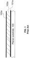
- Fig. 1 a three-layer Fabry-Perot cavity is shown.
- the substrate 100 has deposited thereon a conforming layer 101a of a highly reflective material such as Al.
- Deposited on the aluminum layer 101a is a dielectric conforming layer 102a.
- a conforming absorber layer 103a is subsequently deposited on the dielectric layer 102a.
- Using conventional vacuum coating techniques results in a thin film optically variable filter upon a substrate wherein each layer has a substantially uniform thickness.
- each layer will be a uniform thickness whether conforming layers or nonconforming layers are deposited, providing a same optical effect when applied to a planar surface such as that in Fig. 1 .
- the optical effects obtained for conforming or non-conforming layers will be different when the substrate has a microstructured surface.
- Non-conforming layers will fill in voids where conforming layers simply conform to the microstructured surface so that they are substantially uniform in thickness.
- a thin-film Fabry-Perot filter functions as a color changing element; as the angle of light incident upon the cavity is varied between the light source and the viewer, the color varies as a function of the path length through the dielectric layer varying with the change in angle.
- Fig. 2a a substrate is shown in cross-section where microstructures 201 pointing upward from the substrate are shown, and wherein the height of the upstanding structures is uniform.
- a three dimensional perspective isometric view is shown in Fig. 2b and a top view is shown in Fig. 2c .
- Figs. 3a through 3c illustrate an example wherein the microstructures within the substrate 300 are in the form of grooves 301 of varying depth within the substrate.
- Figs 4a through 4c show a substrate 400 wherein a grating formed of grooves 401 of a first depth are bound by deeper framing grooves 402 within the substrate.
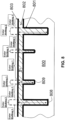
- Fig. 5a and 5b show a cross section of a substrate coated with a coating material where the layer has been grown atom by atom by conventional vacuum coating processes as evaporation and sputtering.
- the layer conforms to the substrate following the original microstructure of the surface. If for example a 3 layer RI D /A is coated, the same color by thin film interference will be seen everywhere in the substrate since the thickness of the dielectric is constant as shown in Fig. 6 .
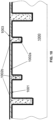
- a substrate 600 having embossed grooves 612 and 614 of varying depth shows a reflector layer 601 of a first uniform thickness, a dielectric layer 602 of a second uniform thickness, and an absorber layer 603 of a third uniform thickness coated over the substrate 600 wherein of the layers are conforming layers.
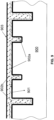
- Fig. 7 the same substrate as shown in Fig. 6 is used however one of the coating layers in Fig. 7 is non-conforming providing a functionally differing device from Fig. 6 .
- a substrate 700 is shown having a conforming reflector layer 701 of uniform thickness coated directly thereon.
- the reflector layer is a non-conforming coating of dielectric material, which fills in the grooves within the reflector coated substrate and has an upper substantially planar layer.
- the dielectric layer 702 has a varying thickness, in cross-section, as shown. Two different thicknesses result when the dielectric layer is coated over substrate 700 due to the two different depths within the microstructured substrate 700.
- the two different depths of the dielectric spacer layer provide two different color shifting regions, where the color shifts from a different first color, to a different second color in the regions of different thickness.
- a thickness difference in the spacer or dielectric layer is required.
- the thickness difference in the spacer layer is considerably larger than the combined thickness of the adjacent two layers 703 and 701.
- An absorber layer 703 having a substantially uniform thickness is shown over the dielectric layer 702.
- the absorber layer 703 could be a conforming layer or a non-conforming layer since it is a planar layer applied onto a planar surface.
- a conforming absorber layer is used, typical of conventional color-shifting filters.
- the thickness of the dielectric layer can be selectively controlled by providing microstructures having selectively chosen depths or protuberances in the form of upstanding features, as the dielectric layer essentially fills in voids resulting in a varying of its thickness.
- color shifting regions 706 having a first color shifting range of colors and color shifting regions 708 have a second color shifting range of colors.
- Typical thickness ranges for the absorber layer would be 20 Angstroms to 150 Angstroms depending upon which metal was selected.
- the reflectivity of the reflector layer is preferably at least 20% to provide an adequate visual effect from the device and the dielectric spacer layer could vary be as much as 800 nm.
- a non-conforming or conforming dielectric When a non-conforming or conforming dielectric is applied to a single level macrostructure surface such as that of Fig. 1 , two different colors will be produced by thin film interference corresponding to the different thickness of the planarizing dielectric layer as the angle of incidence increases. Notice that the reflector and absorber layers applied are conforming layers. Since a dielectric polymeric layer tends to have an index of refraction in between 1.5 and 1.7, the thin-film interference will produce colors that shift from high to low wavelengths as the angle of illumination increases.
- a release layer can be applied in between the substrate and the deposited layers with the intention to strip off the multilayer to make micro multi-color shifting microstructured pigment flakes.
- the release layer can also be used to transfer the multilayer to another object. If the device is intended to make thread, yam, or foils it may not require the use of release layers. Such flakes are typically less than 100 mm or equal thereto, across a longest length. The difference shown in the figures between the two dielectric thicknesses are exaggerated.
- the aspect ratio for the microstructured character is 100-500nm of depth for a line width that is typically 1-5um.
- the microstructure within the substrate can represent symbols, logos, grating, frames, peaks/valleys, etc. as shown in Figs 2a through 3c .
- the color shifting coating provides a way in which these features, such as logos, etc., can be enhanced.
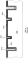
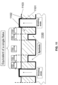
- Fig. 8 grooves in substrate 800 are of two different depths.
- the non-conforming dielectric layer 802 is deposited over the conforming reflector layer 801 and an absorbing layer 803 is applied thereover, the resulting structure is a Fabry-Perot color-shifting filter having three distinct ranges of color shifting.
- the non-conforming layer provides a planarizing smoothing effect upon which layer 803 is deposited conforming to this planarized layer. As the number of distinct levels or depths within the microstructure increases the number of ranges of color shifting increases accordingly.
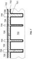
- Fig. 9 illustrates an embodiment of the invention wherein a microstructured substrate 900 is coated with a conforming reflector layer 901 and where conforming and non-conforming dielectric layers 902a and 902b respectively are used adjacent to one another in a same device.
- a planar absorber layer 903 is coated over the non-conforming dielectric layer 902b.
- This planar layer 903 could be a conforming or a non-conforming layer since it is being applied to a planar surface.
- three different color ranges are seen due to the three thicknesses of the combined dielectric layers.
- generally non-conforming polymeric dielectric layers have a lower refractive index than standard inorganic oxides layers.
- Fig. 9 exemplifies a microstructured foil.
- the microstructure substrate 1000 is shown coated with a reflector layer 1001, which is coated with a conforming first dielectric layer 1002a.
- a second non-confirming polymeric layer 1002b is coated and only fills in trenches or grooves within the coated substrate 1001.
- Absorber layer 1003 is coated as a top layer forming together with the other coated layers a color-shifting filter. In practice this could be achieved by eliminating the top of the polymeric dielectric of Fig. 9 , for example by ion bombarding under vacuum until reaching suitable level of the inorganic oxide layer prior to the deposition of the absorber layer.
- a substrate 1100 having protuberances or upstanding structures is shown.
- This example lends itself more to applying a release layer than the previously described structures. If a release layer is applied, it is first applied prior to depositing the reflector layer 1101, so that the reflector layer and subsequent deposited layer can together be released from the substrate.
- the organic non-conforming dielectric layer 1102 is deposited to a level lower than the higher areas that will be used as braking points to produce the shaped flakes. Only the thin layers corresponding to the reflector 1101 and absorber 1103 will be in the top of these areas.
- these flakes will have different properties when viewed from different sides.
- the flakes When viewed from the side having a reflector layer, the flakes will simply be reflective. However on the opposite side, a viewer with magnification would see the logos or symbols with a color shifting exhibited surrounded by a background of a different color. From the reflective side logos may be discernible however the color will correspond to that of the reflector layer.
- the top of the higher areas have a thin metal layer exposed surrounded by a dielectric layer.
- the top areas can be used as seed point to grow preferentially other layers, for example one can perform electroplating using the exposed metallic layer as electrodes.
- Such devices can be used for other applications such as for sensors where micro exposed metallic layers are necessary.
- the multilayer Fabry-Perot filter is formed of a five-layer structure with layers A/D/R/D/A. Since the reflector layer 1201 is shown as a central layer, color shifting will be seen from both sides of this flake after it is released from the substrate 1200. Upon the substrate is a release layer, not shown and a first absorber layer 1203a. Upon the first absorber layer is a first non-conforming dielectric layer 1202a. The reflector layer 1201 is shown deposited upon the first dielectric layer 1202a. A second non-conforming dielectric layer 1202b is deposited over the reflector layer 1201 and a conforming 2nd absorber layer 1203b is deposited over the second non-conforming dielectric layer 1202b.
- the shaped flakes After releasing the multilayer, the shaped flakes when broken along the breaking lines, exhibit on side 1 the Symbol 2 with a non-shifting color corresponding to Absorber /Reflector and symbol 1 corresponding to a color shifting (CS4) from the multilayer Absorber/Dielectric/Reflector surrounded by another color shifting background (CS3).
- CS4 color shifting
- Fig. 13 differs to the example shown in Fig. 11 in the optical design used to create the thin-film interference.
- a microstructured substrate 1300 is shown having a first conforming absorber layer 1301 instead of a reflector layer.
- a non conforming dielectric layer 1302 is coated over layer 1301 and a conforming 2nd absorber layer 1303 is coated over the dielectric layer.
- Thin film interference is obtained by this three-layer Absorber/Dielectric/ Absorber design.
- Such optical designs are semi transparent. If coated on a substrate with the features up shown in a previous example with logos with a single height, the shaped flakes will show the symbols with a different color than their background in both sides. If the symbols have more than one height in cross-section, different areas of the logo will show different colors.
- the variation in the thickness of the dielectric layer is much greater than the thickness of each of the two layers adjacent the dielectric layer.
- this invention allows for the fabrication of filters which have a varying thickness spacer layer and wherein the thickness can be precisely controlled. This allows for a single layer be it either continuous or segmented to provide different color shifting in different regions across the filter as function of the spacer layer thickness. Either flakes or foil can be made.
- the nonconforming dielectric layer is coated over a conforming layer and covered with a conforming layer, however the dielectric layer could be coated over a non-conforming layer or may be covered with a non-conforming layer.
Landscapes
- Physics & Mathematics (AREA)
- General Physics & Mathematics (AREA)
- Optics & Photonics (AREA)
- Chemical & Material Sciences (AREA)
- Organic Chemistry (AREA)
- Business, Economics & Management (AREA)
- Accounting & Taxation (AREA)
- Finance (AREA)
- Optical Filters (AREA)
- Devices For Indicating Variable Information By Combining Individual Elements (AREA)
Claims (10)
- Un dispositif de sécurité à changement de couleur comprenant :une première couche (901) ayant une surface microstructurée ;une deuxième couche plane (903) ;une couche conformante diélectrique (902a) et une couche non conformante diélectrique (902b) disposées entre la première couche (901) et la deuxième couche (903), la couche conformante diélectrique (902a) ayant une surface en contact avec et complémentaire de la surface microstructurée de la première couche (901), la couche non conformante diélectrique (902b) est une couche de polymère à indice de réfraction bas qui est combinée avec un matériau diélectrique inorganique à indice de réfraction élevé, et formée à partir d'un matériau diélectrique non conformant de remplissage à même de remplir des rainures au sein de la couche conformante diélectrique (902a) afin de former la couche diélectrique non conformante (902b) et de former une surface plane par-dessus une région continue de la surface microstructurée ; etun substrat (900) supportant la première couche (901), le substrat (900) ayant des microstructures correspondant à la surface microstructurée de la première couche (901),dans lequel la première couche (901) est une couche réflecteur, dans lequel la deuxième couche (903) est une couche d'absorption, et dans lequel une coupe transversale de la couche non conformante diélectrique (902a) a une épaisseur variable de telle sorte que l'au moins une région est substantiellement plus épaisse qu'une région adjacente plus mince de ladite couche, et dans lequel une différence de couleur visible est vue lorsque le filtre est visualisé à travers cette région et la région adjacente à partir d'un même emplacement simultanément lorsque de la lumière est incidente sur le filtre,dans lequel le substrat (900) est enduit respectivement de la première couche (901), de la couche diélectrique conformante (902a), de la couche diélectrique non conformante (902b), et de la deuxième couche (903),dans lequel la première couche (901), la deuxième couche (903) et la couche non conformante diélectrique forment ensemble une cavité de Fabry-Perot, etdans lequel les microstructures définissent un logo ou un repère discernable.
- Un dispositif de sécurité à changement de couleur tel que revendiqué dans la revendication 1 dans lequel les microstructures ont des profondeurs sélectivement choisies, ou des protubérances sous la forme de caractéristiques dressées.
- Un dispositif de sécurité à changement de couleur tel que revendiqué dans la revendication 1 dans lequel des microstructures ont un certain nombre de niveaux ou de profondeurs distincts.
- Un dispositif de sécurité à changement de couleur tel que revendiqué dans la revendication 1 dans lequel les rainures sont de deux profondeurs différentes.
- Un dispositif de sécurité à changement de couleur tel que défini dans la revendication 1, dans lequel la cavité de Fabry-Perot forme une paillette.
- Un dispositif de sécurité à changement de couleur tel que défini dans la revendication 1, dans lequel la première couche (901), ou la deuxième couche (903), a une épaisseur substantiellement uniforme, laquelle varie de 20 % au plus.
- Un dispositif de sécurité à changement de couleur tel que revendiqué dans la revendication 1, dans lequel une différence d'épaisseur d'une coupe transversale de la couche non conformante diélectrique fait plus de 1/8 de longueurs d'onde de lumière visible et moins de 8 quarts de longueurs d'onde de lumière visible.
- Un dispositif de sécurité à changement de couleur tel que revendiqué dans n'importe laquelle des revendications précédentes, dans lequel la couche diélectrique non conformante a une épaisseur variable de deux épaisseurs différentes du fait des deux profondeurs différentes au sein du substrat microstructuré, et les deux profondeurs différentes de la couche d'espacement diélectrique fournissent deux régions à changement de couleur différentes, où la couleur varie d'une première couleur différente à une deuxième couleur différente dans les régions d'épaisseur différente.
- Un dispositif de sécurité à changement de couleur tel que revendiqué dans la revendication 1 dans lequel la cavité de Fabry-Perot est sous la forme d'une feuille microstructurée.
- Un procédé de fabrication d'un dispositif de sécurité tel que défini dans la revendication 1, comprenantle fait de fournir un substrat microstructuré (900) ;le fait d'enduire le substrat microstructuré d'un premier enduit réfléchissant (901) qui se conforme au substrat à microstructures (900) ;le fait d'enduire l'enduit réfléchissant (901) d'un enduit diélectrique conformant (902a) et d'un enduit de nivellement diélectrique non conformant (902b) qui remplit au moins partiellement des vides au sein de l'enduit microstructuré ; etle fait d'enduire l'enduit de nivellement diélectrique non conformant (902b) d'un deuxième enduit d'absorption (903).
Applications Claiming Priority (2)
| Application Number | Priority Date | Filing Date | Title |
|---|---|---|---|
| US201161500432P | 2011-06-23 | 2011-06-23 | |
| EP12172029.6A EP2538247B1 (fr) | 2011-06-23 | 2012-06-14 | Eléments de sécurité multi-couleurs à variation chromatique |
Related Parent Applications (2)
| Application Number | Title | Priority Date | Filing Date |
|---|---|---|---|
| EP12172029.6A Division EP2538247B1 (fr) | 2011-06-23 | 2012-06-14 | Eléments de sécurité multi-couleurs à variation chromatique |
| EP12172029.6A Division-Into EP2538247B1 (fr) | 2011-06-23 | 2012-06-14 | Eléments de sécurité multi-couleurs à variation chromatique |
Publications (2)
| Publication Number | Publication Date |
|---|---|
| EP3351981A1 EP3351981A1 (fr) | 2018-07-25 |
| EP3351981B1 true EP3351981B1 (fr) | 2025-04-02 |
Family
ID=46969959
Family Applications (2)
| Application Number | Title | Priority Date | Filing Date |
|---|---|---|---|
| EP12172029.6A Active EP2538247B1 (fr) | 2011-06-23 | 2012-06-14 | Eléments de sécurité multi-couleurs à variation chromatique |
| EP18158830.2A Active EP3351981B1 (fr) | 2011-06-23 | 2012-06-14 | Dispositifs à variations chromatiques multiples |
Family Applications Before (1)
| Application Number | Title | Priority Date | Filing Date |
|---|---|---|---|
| EP12172029.6A Active EP2538247B1 (fr) | 2011-06-23 | 2012-06-14 | Eléments de sécurité multi-couleurs à variation chromatique |
Country Status (4)
| Country | Link |
|---|---|
| US (2) | US9561682B2 (fr) |
| EP (2) | EP2538247B1 (fr) |
| CN (2) | CN102837528B (fr) |
| HK (1) | HK1250397A1 (fr) |
Families Citing this family (26)
| Publication number | Priority date | Publication date | Assignee | Title |
|---|---|---|---|---|
| EP2538247B1 (fr) | 2011-06-23 | 2018-04-11 | Viavi Solutions Inc. | Eléments de sécurité multi-couleurs à variation chromatique |
| CN103921582B (zh) * | 2014-02-24 | 2017-03-29 | 苏州大学 | 一种变色烫印膜及其制造方法 |
| WO2017000069A1 (fr) * | 2015-06-30 | 2017-01-05 | Spectral Devices Inc. | Filtre de fabry-pérot pixelisé flexible |
| EP3269780A1 (fr) | 2016-06-27 | 2018-01-17 | Viavi Solutions Inc. | Flocons hautement chromatiques |
| JP6716500B2 (ja) | 2016-06-27 | 2020-07-01 | ヴァイアヴィ・ソリューションズ・インコーポレイテッドViavi Solutions Inc. | 光学デバイス |
| US12187900B2 (en) | 2016-06-27 | 2025-01-07 | Viavi Solutions Inc. | High chromaticity pigment flakes and foils |
| DE102016010078A1 (de) * | 2016-08-18 | 2018-02-22 | Giesecke+Devrient Currency Technology Gmbh | Optisch variables Sicherheitselement mit Dünnschichtelement |
| GB2553555B (en) * | 2016-09-08 | 2019-12-11 | De La Rue Int Ltd | Security devices and methods of manufacture thereof |
| US10357991B2 (en) | 2016-12-19 | 2019-07-23 | Viavi Solutions Inc. | Security ink based security feature |
| DE102017003603A1 (de) * | 2017-04-12 | 2018-10-18 | Giesecke+Devrient Currency Technology Gmbh | Sicherheitselement mit farbigem Merkmalsbereich |
| CN111433030B (zh) | 2017-09-29 | 2021-09-14 | 耐克创新有限合伙公司 | 结构着色的物品以及用于制造和使用结构着色的物品的方法 |
| US10899930B2 (en) | 2017-11-21 | 2021-01-26 | Viavi Solutions Inc. | Asymmetric pigment |
| GB2572550B (en) * | 2018-03-28 | 2020-07-22 | De La Rue Int Ltd | Optical device and method of manufacture thereof |
| US12552939B2 (en) | 2018-06-29 | 2026-02-17 | Viavi Solutions Inc. | Optical devices with functional molecules |
| US10962694B2 (en) | 2018-11-02 | 2021-03-30 | Viavi Solutions Inc. | Stepped structure optical filter |
| CN111845148B (zh) | 2019-04-24 | 2022-04-05 | 中钞特种防伪科技有限公司 | 光学防伪元件及其制作方法 |
| EP3969947A1 (fr) | 2019-06-26 | 2022-03-23 | Nike Innovate C.V. | Articles structuralement colorés et procédés de fabrication et d'utilisation d'articles structuralement colorés |
| US20210022444A1 (en) | 2019-07-26 | 2021-01-28 | Nike, Inc. | Structurally-colored articles and methods for making and using structurally-colored articles |
| US11986042B2 (en) | 2019-10-21 | 2024-05-21 | Nike, Inc. | Structurally-colored articles and methods for making and using structurally-colored articles |
| CN110703374B (zh) * | 2019-11-05 | 2025-05-16 | 苏州大学 | 基于法布里珀罗共振的光学介质金属超构光栅 |
| WO2021243223A2 (fr) * | 2020-05-29 | 2021-12-02 | Nike, Inc. | Articles structuralement colorés et procédés de fabrication et d'utilisation d'articles structuralement colorés |
| US11129444B1 (en) | 2020-08-07 | 2021-09-28 | Nike, Inc. | Footwear article having repurposed material with concealing layer |
| US11241062B1 (en) | 2020-08-07 | 2022-02-08 | Nike, Inc. | Footwear article having repurposed material with structural-color concealing layer |
| US11889894B2 (en) | 2020-08-07 | 2024-02-06 | Nike, Inc. | Footwear article having concealing layer |
| CN118176115A (zh) * | 2021-11-12 | 2024-06-11 | Viavi科技有限公司 | 包括具有两种或更多种类型像素的图像的制品 |
| FR3156699B1 (fr) * | 2023-12-14 | 2025-10-31 | Surys | Composant optique de sécurité |
Family Cites Families (14)
| Publication number | Priority date | Publication date | Assignee | Title |
|---|---|---|---|---|
| US587789A (en) | 1897-08-10 | Car-fender | ||
| US5877895A (en) | 1995-03-20 | 1999-03-02 | Catalina Coatings, Inc. | Multicolor interference coating |
| US6761959B1 (en) | 1999-07-08 | 2004-07-13 | Flex Products, Inc. | Diffractive surfaces with color shifting backgrounds |
| GB0015873D0 (en) | 2000-06-28 | 2000-08-23 | Rue De Int Ltd | Optically variable security device |
| DE10232245B4 (de) * | 2002-07-17 | 2008-06-12 | Leonhard Kurz Gmbh & Co. Kg | Optisch variables Element mit variierender Distanzschicht-Dicke |
| CN1597334B (zh) * | 2003-07-14 | 2011-03-30 | Jds尤尼费斯公司 | 防伪线和在薄板上制造光学可变装置的方法 |
| DE102004032565A1 (de) * | 2004-07-05 | 2006-02-16 | Giesecke & Devrient Gmbh | Sicherheitselement mit Farbkippeffekt |
| US7209386B2 (en) * | 2004-07-06 | 2007-04-24 | Macronix International Co., Ltd. | Charge trapping non-volatile memory and method for gate-by-gate erase for same |
| EP1771752B1 (fr) * | 2004-07-21 | 2020-10-07 | ROLIC Technologies AG | Elément optique anisotrope et méthode de son procédé de fabrication |
| AU2006202315B2 (en) | 2005-06-17 | 2011-01-27 | Viavi Solutions Inc. | Covert security coating |
| CA2656506A1 (fr) * | 2009-02-27 | 2010-08-27 | Bank Of Canada | Dispositif de verification des caracteristiques de securite |
| EP2230539B1 (fr) * | 2009-03-19 | 2019-12-04 | Viavi Solutions Inc. | Formation de motifs dans une couche d'espaceur dans un filtre d'interférence |
| EP2538247B1 (fr) * | 2011-06-23 | 2018-04-11 | Viavi Solutions Inc. | Eléments de sécurité multi-couleurs à variation chromatique |
| DE102011119598A1 (de) * | 2011-11-29 | 2013-05-29 | Ovd Kinegram Ag | Optisch variables Element |
-
2012
- 2012-06-14 EP EP12172029.6A patent/EP2538247B1/fr active Active
- 2012-06-14 EP EP18158830.2A patent/EP3351981B1/fr active Active
- 2012-06-22 US US13/530,918 patent/US9561682B2/en active Active
- 2012-06-25 CN CN201210211931.7A patent/CN102837528B/zh active Active
- 2012-06-25 CN CN201710258114.XA patent/CN107089067B/zh active Active
-
2016
- 2016-12-12 US US15/375,962 patent/US10300729B2/en active Active
-
2018
- 2018-07-27 HK HK18109767.2A patent/HK1250397A1/en unknown
Also Published As
| Publication number | Publication date |
|---|---|
| EP2538247A2 (fr) | 2012-12-26 |
| EP3351981A1 (fr) | 2018-07-25 |
| HK1250397A1 (en) | 2018-12-14 |
| US20170087918A1 (en) | 2017-03-30 |
| US20120326430A1 (en) | 2012-12-27 |
| CN102837528A (zh) | 2012-12-26 |
| US9561682B2 (en) | 2017-02-07 |
| EP2538247B1 (fr) | 2018-04-11 |
| EP2538247A3 (fr) | 2013-11-13 |
| CN107089067A (zh) | 2017-08-25 |
| CN107089067B (zh) | 2019-02-19 |
| CN102837528B (zh) | 2017-05-17 |
| US10300729B2 (en) | 2019-05-28 |
Similar Documents
| Publication | Publication Date | Title |
|---|---|---|
| EP3351981B1 (fr) | Dispositifs à variations chromatiques multiples | |
| KR101371431B1 (ko) | 은폐 보안 코팅 | |
| EP2024447B1 (fr) | Matrice avec pigments à diffraction d'ordre nul | |
| US10112432B2 (en) | Security device | |
| JP2016513271A5 (fr) | ||
| US11001720B2 (en) | Flakes with undulate borders and methods of forming thereof | |
| HK1240542A1 (en) | Multi color-shifting devices | |
| HK1240542B (zh) | 多色移装置 | |
| HK1179925A (en) | Multi-color-shifting devices | |
| HK1179925B (en) | Multi-color-shifting devices |
Legal Events
| Date | Code | Title | Description |
|---|---|---|---|
| PUAI | Public reference made under article 153(3) epc to a published international application that has entered the european phase |
Free format text: ORIGINAL CODE: 0009012 |
|
| STAA | Information on the status of an ep patent application or granted ep patent |
Free format text: STATUS: THE APPLICATION HAS BEEN PUBLISHED |
|
| AC | Divisional application: reference to earlier application |
Ref document number: 2538247 Country of ref document: EP Kind code of ref document: P |
|
| AK | Designated contracting states |
Kind code of ref document: A1 Designated state(s): AL AT BE BG CH CY CZ DE DK EE ES FI FR GB GR HR HU IE IS IT LI LT LU LV MC MK MT NL NO PL PT RO RS SE SI SK SM TR |
|
| REG | Reference to a national code |
Ref country code: HK Ref legal event code: DE Ref document number: 1250397 Country of ref document: HK |
|
| STAA | Information on the status of an ep patent application or granted ep patent |
Free format text: STATUS: REQUEST FOR EXAMINATION WAS MADE |
|
| 17P | Request for examination filed |
Effective date: 20190121 |
|
| RBV | Designated contracting states (corrected) |
Designated state(s): AL AT BE BG CH CY CZ DE DK EE ES FI FR GB GR HR HU IE IS IT LI LT LU LV MC MK MT NL NO PL PT RO RS SE SI SK SM TR |
|
| STAA | Information on the status of an ep patent application or granted ep patent |
Free format text: STATUS: EXAMINATION IS IN PROGRESS |
|
| 17Q | First examination report despatched |
Effective date: 20191212 |
|
| RAP3 | Party data changed (applicant data changed or rights of an application transferred) |
Owner name: VIAVI SOLUTIONS INC. |
|
| P01 | Opt-out of the competence of the unified patent court (upc) registered |
Effective date: 20230530 |
|
| GRAP | Despatch of communication of intention to grant a patent |
Free format text: ORIGINAL CODE: EPIDOSNIGR1 |
|
| STAA | Information on the status of an ep patent application or granted ep patent |
Free format text: STATUS: GRANT OF PATENT IS INTENDED |
|
| RIC1 | Information provided on ipc code assigned before grant |
Ipc: B42D 15/00 20060101ALN20241015BHEP Ipc: G02B 5/20 20060101ALI20241015BHEP Ipc: G02B 5/28 20060101AFI20241015BHEP |
|
| RIC1 | Information provided on ipc code assigned before grant |
Ipc: B42D 15/00 20060101ALN20241029BHEP Ipc: G02B 5/20 20060101ALI20241029BHEP Ipc: G02B 5/28 20060101AFI20241029BHEP |
|
| INTG | Intention to grant announced |
Effective date: 20241114 |
|
| GRAS | Grant fee paid |
Free format text: ORIGINAL CODE: EPIDOSNIGR3 |
|
| GRAA | (expected) grant |
Free format text: ORIGINAL CODE: 0009210 |
|
| STAA | Information on the status of an ep patent application or granted ep patent |
Free format text: STATUS: THE PATENT HAS BEEN GRANTED |
|
| AC | Divisional application: reference to earlier application |
Ref document number: 2538247 Country of ref document: EP Kind code of ref document: P |
|
| AK | Designated contracting states |
Kind code of ref document: B1 Designated state(s): AL AT BE BG CH CY CZ DE DK EE ES FI FR GB GR HR HU IE IS IT LI LT LU LV MC MK MT NL NO PL PT RO RS SE SI SK SM TR |
|
| REG | Reference to a national code |
Ref country code: GB Ref legal event code: FG4D |
|
| REG | Reference to a national code |
Ref country code: CH Ref legal event code: EP |
|
| REG | Reference to a national code |
Ref country code: IE Ref legal event code: FG4D |
|
| REG | Reference to a national code |
Ref country code: DE Ref legal event code: R096 Ref document number: 602012081455 Country of ref document: DE |
|
| PGFP | Annual fee paid to national office [announced via postgrant information from national office to epo] |
Ref country code: GB Payment date: 20250627 Year of fee payment: 14 |
|
| PGFP | Annual fee paid to national office [announced via postgrant information from national office to epo] |
Ref country code: FR Payment date: 20250626 Year of fee payment: 14 |
|
| REG | Reference to a national code |
Ref country code: NL Ref legal event code: MP Effective date: 20250402 |
|
| PG25 | Lapsed in a contracting state [announced via postgrant information from national office to epo] |
Ref country code: NL Free format text: LAPSE BECAUSE OF FAILURE TO SUBMIT A TRANSLATION OF THE DESCRIPTION OR TO PAY THE FEE WITHIN THE PRESCRIBED TIME-LIMIT Effective date: 20250402 |
|
| REG | Reference to a national code |
Ref country code: AT Ref legal event code: MK05 Ref document number: 1781794 Country of ref document: AT Kind code of ref document: T Effective date: 20250402 |
|
| PG25 | Lapsed in a contracting state [announced via postgrant information from national office to epo] |
Ref country code: ES Free format text: LAPSE BECAUSE OF FAILURE TO SUBMIT A TRANSLATION OF THE DESCRIPTION OR TO PAY THE FEE WITHIN THE PRESCRIBED TIME-LIMIT Effective date: 20250402 Ref country code: FI Free format text: LAPSE BECAUSE OF FAILURE TO SUBMIT A TRANSLATION OF THE DESCRIPTION OR TO PAY THE FEE WITHIN THE PRESCRIBED TIME-LIMIT Effective date: 20250402 Ref country code: PT Free format text: LAPSE BECAUSE OF FAILURE TO SUBMIT A TRANSLATION OF THE DESCRIPTION OR TO PAY THE FEE WITHIN THE PRESCRIBED TIME-LIMIT Effective date: 20250804 |
|
| PGFP | Annual fee paid to national office [announced via postgrant information from national office to epo] |
Ref country code: DE Payment date: 20250630 Year of fee payment: 14 |
|
| REG | Reference to a national code |
Ref country code: LT Ref legal event code: MG9D |
|
| PG25 | Lapsed in a contracting state [announced via postgrant information from national office to epo] |
Ref country code: GR Free format text: LAPSE BECAUSE OF FAILURE TO SUBMIT A TRANSLATION OF THE DESCRIPTION OR TO PAY THE FEE WITHIN THE PRESCRIBED TIME-LIMIT Effective date: 20250703 Ref country code: NO Free format text: LAPSE BECAUSE OF FAILURE TO SUBMIT A TRANSLATION OF THE DESCRIPTION OR TO PAY THE FEE WITHIN THE PRESCRIBED TIME-LIMIT Effective date: 20250702 |
|
| PG25 | Lapsed in a contracting state [announced via postgrant information from national office to epo] |
Ref country code: PL Free format text: LAPSE BECAUSE OF FAILURE TO SUBMIT A TRANSLATION OF THE DESCRIPTION OR TO PAY THE FEE WITHIN THE PRESCRIBED TIME-LIMIT Effective date: 20250402 |
|
| PG25 | Lapsed in a contracting state [announced via postgrant information from national office to epo] |
Ref country code: BG Free format text: LAPSE BECAUSE OF FAILURE TO SUBMIT A TRANSLATION OF THE DESCRIPTION OR TO PAY THE FEE WITHIN THE PRESCRIBED TIME-LIMIT Effective date: 20250402 |
|
| PG25 | Lapsed in a contracting state [announced via postgrant information from national office to epo] |
Ref country code: HR Free format text: LAPSE BECAUSE OF FAILURE TO SUBMIT A TRANSLATION OF THE DESCRIPTION OR TO PAY THE FEE WITHIN THE PRESCRIBED TIME-LIMIT Effective date: 20250402 |
|
| PG25 | Lapsed in a contracting state [announced via postgrant information from national office to epo] |
Ref country code: AT Free format text: LAPSE BECAUSE OF FAILURE TO SUBMIT A TRANSLATION OF THE DESCRIPTION OR TO PAY THE FEE WITHIN THE PRESCRIBED TIME-LIMIT Effective date: 20250402 |
|
| PGFP | Annual fee paid to national office [announced via postgrant information from national office to epo] |
Ref country code: CH Payment date: 20250701 Year of fee payment: 14 |
|
| PG25 | Lapsed in a contracting state [announced via postgrant information from national office to epo] |
Ref country code: RS Free format text: LAPSE BECAUSE OF FAILURE TO SUBMIT A TRANSLATION OF THE DESCRIPTION OR TO PAY THE FEE WITHIN THE PRESCRIBED TIME-LIMIT Effective date: 20250702 |
|
| PG25 | Lapsed in a contracting state [announced via postgrant information from national office to epo] |
Ref country code: IS Free format text: LAPSE BECAUSE OF FAILURE TO SUBMIT A TRANSLATION OF THE DESCRIPTION OR TO PAY THE FEE WITHIN THE PRESCRIBED TIME-LIMIT Effective date: 20250802 |
|
| PG25 | Lapsed in a contracting state [announced via postgrant information from national office to epo] |
Ref country code: LV Free format text: LAPSE BECAUSE OF FAILURE TO SUBMIT A TRANSLATION OF THE DESCRIPTION OR TO PAY THE FEE WITHIN THE PRESCRIBED TIME-LIMIT Effective date: 20250402 |
|
| REG | Reference to a national code |
Ref country code: DE Ref legal event code: R097 Ref document number: 602012081455 Country of ref document: DE |
|
| PG25 | Lapsed in a contracting state [announced via postgrant information from national office to epo] |
Ref country code: SM Free format text: LAPSE BECAUSE OF FAILURE TO SUBMIT A TRANSLATION OF THE DESCRIPTION OR TO PAY THE FEE WITHIN THE PRESCRIBED TIME-LIMIT Effective date: 20250402 Ref country code: DK Free format text: LAPSE BECAUSE OF FAILURE TO SUBMIT A TRANSLATION OF THE DESCRIPTION OR TO PAY THE FEE WITHIN THE PRESCRIBED TIME-LIMIT Effective date: 20250402 |
|
| PG25 | Lapsed in a contracting state [announced via postgrant information from national office to epo] |
Ref country code: CZ Free format text: LAPSE BECAUSE OF FAILURE TO SUBMIT A TRANSLATION OF THE DESCRIPTION OR TO PAY THE FEE WITHIN THE PRESCRIBED TIME-LIMIT Effective date: 20250402 |
|
| PG25 | Lapsed in a contracting state [announced via postgrant information from national office to epo] |
Ref country code: EE Free format text: LAPSE BECAUSE OF FAILURE TO SUBMIT A TRANSLATION OF THE DESCRIPTION OR TO PAY THE FEE WITHIN THE PRESCRIBED TIME-LIMIT Effective date: 20250402 |
|
| PG25 | Lapsed in a contracting state [announced via postgrant information from national office to epo] |
Ref country code: RO Free format text: LAPSE BECAUSE OF FAILURE TO SUBMIT A TRANSLATION OF THE DESCRIPTION OR TO PAY THE FEE WITHIN THE PRESCRIBED TIME-LIMIT Effective date: 20250402 Ref country code: SK Free format text: LAPSE BECAUSE OF FAILURE TO SUBMIT A TRANSLATION OF THE DESCRIPTION OR TO PAY THE FEE WITHIN THE PRESCRIBED TIME-LIMIT Effective date: 20250402 |
|
| PG25 | Lapsed in a contracting state [announced via postgrant information from national office to epo] |
Ref country code: IT Free format text: LAPSE BECAUSE OF FAILURE TO SUBMIT A TRANSLATION OF THE DESCRIPTION OR TO PAY THE FEE WITHIN THE PRESCRIBED TIME-LIMIT Effective date: 20250402 |
|
| PG25 | Lapsed in a contracting state [announced via postgrant information from national office to epo] |
Ref country code: MC Free format text: LAPSE BECAUSE OF FAILURE TO SUBMIT A TRANSLATION OF THE DESCRIPTION OR TO PAY THE FEE WITHIN THE PRESCRIBED TIME-LIMIT Effective date: 20250402 |
|
| PLBE | No opposition filed within time limit |
Free format text: ORIGINAL CODE: 0009261 |
|
| STAA | Information on the status of an ep patent application or granted ep patent |
Free format text: STATUS: NO OPPOSITION FILED WITHIN TIME LIMIT |
|
| REG | Reference to a national code |
Ref country code: CH Ref legal event code: L10 Free format text: ST27 STATUS EVENT CODE: U-0-0-L10-L00 (AS PROVIDED BY THE NATIONAL OFFICE) Effective date: 20260211 |
|
| PG25 | Lapsed in a contracting state [announced via postgrant information from national office to epo] |
Ref country code: LU Free format text: LAPSE BECAUSE OF NON-PAYMENT OF DUE FEES Effective date: 20250614 |
|
| REG | Reference to a national code |
Ref country code: BE Ref legal event code: MM Effective date: 20250630 |
|
| 26N | No opposition filed |
Effective date: 20260105 |