EP3350808B1 - Magnetische josephson-übergangsspeicherzelle und schreibschaltung - Google Patents
Magnetische josephson-übergangsspeicherzelle und schreibschaltung Download PDFInfo
- Publication number
- EP3350808B1 EP3350808B1 EP16847602.6A EP16847602A EP3350808B1 EP 3350808 B1 EP3350808 B1 EP 3350808B1 EP 16847602 A EP16847602 A EP 16847602A EP 3350808 B1 EP3350808 B1 EP 3350808B1
- Authority
- EP
- European Patent Office
- Prior art keywords
- current
- phmjj
- write
- read
- bit
- Prior art date
- Legal status (The legal status is an assumption and is not a legal conclusion. Google has not performed a legal analysis and makes no representation as to the accuracy of the status listed.)
- Active
Links
Images



Classifications
-
- G—PHYSICS
- G11—INFORMATION STORAGE
- G11C—STATIC STORES
- G11C11/00—Digital stores characterised by the use of particular electric or magnetic storage elements; Storage elements therefor
- G11C11/21—Digital stores characterised by the use of particular electric or magnetic storage elements; Storage elements therefor using electric elements
- G11C11/44—Digital stores characterised by the use of particular electric or magnetic storage elements; Storage elements therefor using electric elements using super-conductive elements, e.g. cryotron
-
- G—PHYSICS
- G11—INFORMATION STORAGE
- G11C—STATIC STORES
- G11C11/00—Digital stores characterised by the use of particular electric or magnetic storage elements; Storage elements therefor
- G11C11/02—Digital stores characterised by the use of particular electric or magnetic storage elements; Storage elements therefor using magnetic elements
- G11C11/16—Digital stores characterised by the use of particular electric or magnetic storage elements; Storage elements therefor using magnetic elements using elements in which the storage effect is based on magnetic spin effect
- G11C11/165—Auxiliary circuits
- G11C11/1673—Reading or sensing circuits or methods
-
- G—PHYSICS
- G11—INFORMATION STORAGE
- G11C—STATIC STORES
- G11C11/00—Digital stores characterised by the use of particular electric or magnetic storage elements; Storage elements therefor
- G11C11/02—Digital stores characterised by the use of particular electric or magnetic storage elements; Storage elements therefor using magnetic elements
- G11C11/16—Digital stores characterised by the use of particular electric or magnetic storage elements; Storage elements therefor using magnetic elements using elements in which the storage effect is based on magnetic spin effect
-
- G—PHYSICS
- G11—INFORMATION STORAGE
- G11C—STATIC STORES
- G11C11/00—Digital stores characterised by the use of particular electric or magnetic storage elements; Storage elements therefor
- G11C11/02—Digital stores characterised by the use of particular electric or magnetic storage elements; Storage elements therefor using magnetic elements
- G11C11/16—Digital stores characterised by the use of particular electric or magnetic storage elements; Storage elements therefor using magnetic elements using elements in which the storage effect is based on magnetic spin effect
- G11C11/165—Auxiliary circuits
- G11C11/1675—Writing or programming circuits or methods
Definitions
- the present invention relates generally to quantum and classical digital superconducting circuits, and specifically to a superconducting phase-controlled hysteretic magnetic Josephson junction JMRAM memory cell.
- Superconducting digital technology has provided computing and/or communications resources that benefit from unprecedented high speed, low power dissipation, and low operating temperature.
- superconducting digital technology has lacked random-access memory (RAM) with adequate capacity and speed relative to logic circuits. This has been a major obstacle to industrialization for current applications of superconducting technology in telecommunications and signal intelligence, and can be especially forbidding for high-end and quantum computing. All concepts currently considered for superconducting memory have been based on quantization of magnetic flux quanta in a superconducting inductive loop.
- Such memories can be readily adapted to high speed register files given a foundry process with adequate yield, but can never achieve the integration density of complementary metal-oxide semiconductor (CMOS), as they are fundamentally limited by the size of the inductive loop.
- CMOS complementary metal-oxide semiconductor
- One hybrid memory solution has been proposed where the memory core implements CMOS technology and the bit-line detection is done with Josephson devices. However, such a configuration yields only nominally higher performance than standard CMOS and suffers from relatively high power dissipation for a cryogenic environment.
- Document XP055378909 discloses a nanopillar Josephson junctions with a minimum feature size of 50 nm and magnetic barriers exhibiting magnetic pseudo-spin-valve behavior at 4K. With a bias current higher than I c8 , these devices allow current-induced magnetization switching that results in tenfold changes in I c8 . The current-induced magnetic switching is consistent with spin-transfer torque models for room-temperature magnetic devices. It is disclosed that devices that combine superconducting and spintronic functions show promise for the development of a nanoscale, nonvolatile, cryogenic memory technology.
- Document XP055379153 discloses a scanning superconducting quantum interference device microscope to image the spontaneous zero-field currents in superconducting networks of temperature-controlled ⁇ -junctions with weakly ferromagnetic barriers. We find an onset of spontaneous supercurrents at the 0- ⁇ transition temperature of the junctions, T ⁇ ⁇ 3K. We image the currents in non-uniformly frustrated arrays consisting of cells with even and odd numbers of ⁇ -junctions. Such arrays are attractive model systems for studying the exotic phases of the two-dimensional XY-model and achieving scalable adiabatic quantum computers.
- JMRAM Josephson magnetic random access memory
- JMRAM Josephson magnetic random access memory
- PHMJJ phase hysteretic magnetic Josephson junction
- PHMJJ phase hysteretic magnetic Josephson junction
- the PHMJJ including outer layers of superconducting material and one or more barrier including internal thin film layers of ferromagnetic material comprising a hard ferromagnetic layer having a substantially fixed magnetization and a soft ferromagnetic layer
- the PHMJJ is magnetically coupled to a word-write line (WLW) and to a bit-write-line (BLW) and is configured to store the digital state corresponding to anyone of a first binary state and a second binary state, wherein in response to PHMJJ being is the first binary state, the PHMJJ is configured to generate a spontaneous supercurrent in a conducting loop through the PHMJJ;
- said JMRAM cell further comprising at least one Josephson junction
- the present invention relates generally to quantum and classical digital superconducting circuits, and specifically to a superconducting phase-controlled hysteretic magnetic Josephson junction JMRAM.
- the JMRAM system implements an array of JMRAM memory cells that each includes a phase hysteretic magnetic Josephson junction (PHMJJ) including ferromagnetic materials in an associated barrier.
- the PHMJJ is configured as a junction switchable between a zero state and a ⁇ -state that is configured to generate a superconducting phase based on the digital state stored therein.
- Each of the JMRAM memory cells includes an at least one Josephson junction (e.g., a pair of Josephson junctions in parallel with the PHMJJ).
- the PHMJJ is configured to store a digital state corresponding to one of a first binary state (e.g., logic-1) or a second binary state (e.g., logic-0) in response to a word-write current and a bit-write current associated with the PHMJJ.
- the first binary state corresponds to a positive ⁇ -state, in which a superconducting phase is provided.
- Word-write and bit-write currents are each provided on dedicated word-write and bit-write lines, and set the logic state of the PHMJJ based on respective current flow directions relative to each other.
- the PHMJJ includes a directional write element that is configured to generate a directional bias current through the PHMJJ during a data write operation.
- the PHMJJ is forced into the positive ⁇ -state to provide the superconducting phase in a predetermined direction.
- the PHMJJ of each of the JMRAM memory cells of the array can provide an indication of the stored digital state in response to a word-read current and a bit-read current.
- the superconducting phase can thus lower a critical current associated with the at least one Josephson junction of each of the JMRAM memory cells of a row of the array. Therefore, the word-read current and the bit-read current can be provided to trigger the Josephson junction(s) to change a voltage on the associated bit-read line based on the PHMJJ storing the first binary state, and to not trigger based on the PHMJJ storing a digital state corresponding to the second binary state.
- the bit-read line can have a voltage having a magnitude that varies based on whether the digital state of the PHMJJ corresponds to the binary logic-1 state or the binary logic-0 state (e.g., between a non-zero and a zero amplitude).
- the term "trigger" with respect to Josephson junctions describes the phenomenon of the Josephson junction generating a discrete voltage pulse in response to a current flow through the Josephson junction exceeding a critical current.
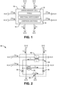
- FIG. 1 illustrates an example of a JMRAM memory cell 10.
- the JMRAM memory cell 10 can correspond to one of a plurality of JMRAM memory cells that are arranged in an array as rows and columns, as described in greater detail herein.
- the JMRAM memory cell 10 includes a word-write line WLW and a word-read line WLR that each pass through the JMRAM memory cell 10.
- the word-write line WLW conducts a word-write current I WW during a data write operation and the word-read line WLR conducts a word-read current I WR during a data read operation.
- the word-write current I WW can correspond to a word-write current associated with a row of JMRAM memory cells in an array
- the word-read current I WR can correspond to a word-read current associated with the row of JMRAM memory cells in the array.
- the word-write and word-read lines WLW and WLR can likewise be coupled to adjacent JMRAM memory cells in a given row on either side of the JMRAM memory cell 10.
- the word-read and word-write currents I WW and I WR flow through all of the JMRAM memory cell systems in the row, including the JMRAM memory cell 10, during the respective data write and data read operations.
- the JMRAM memory cell 10 includes a bit-write line BLW and a bit-read line BLR that each pass through the JMRAM memory cell 10.
- the bit-write line BLW conducts a bit-write current I BW during the data write operation and the bit-read line BLR conducts a bit-read current I BR .
- the bit-read current I BR can be provided on the bit-read line BLR substantially constantly, and not just during data read operations.
- the bit-write current I BW can correspond to a bit-write current associated with a column of JMRAM memory cells in the array
- the bit-read current I BR can correspond to a bit-read current associated with the column of JMRAM memory cells in the array.
- bit-write and bit-read lines BLW and BLR can likewise be coupled to adjacent JMRAM memory cells in a given column above and below the JMRAM memory cell 10.
- bit-write and bit-read currents I BW and I BR flow through all of the JMRAM memory cell systems in the column, including the JMRAM memory cell 10, during the respective data write and data read operations.
- the JMRAM memory cell 10 also includes a phase hysteretic magnetic Josephson junction (PHMJJ) 12 that is configured to store a digital state corresponding to one of a first binary state (e.g., logic-1) or a second binary state (e.g., logic-0).
- PHMJJ 12 includes ferromagnetic materials in associated barriers to be configured as a switchable ⁇ -junction.
- the PHMJJ 12 can include outer layers of superconducting material, such as Niobium (Nb), and one or more internal thin film layers of ferromagnetic materials.
- the thin film layers of ferromagnetic materials include one or more "hard” ferromagnetic layers having a substantially fixed magnetic field and one or more "soft” ferromagnetic layers that are changed as a result of magnetic fields generated locally by orthogonal electrical currents.
- the PHMJJ 12 can include one or more additional layers, such as oxide layers, that are interleaved with the superconducting and/or ferromagnetic layers.
- the JMRAM memory cell 10 includes at least one Josephson junction 14 that is triggered during the data read operation in response to the respective word-read and bit-read currents I WR and I BR to indicate that the PHMJJ 12 is in the first binary state, or not triggered to indicate that the PHMJJ 12 is in the second binary state, as described in greater detail herein.
- the PHMJJ 12 In response to the magnetic fields generated locally by orthogonal electrical currents, the PHMJJ 12 is set to a ⁇ -state in which the PHMJJ 12 generates a superconducting phase.
- the "superconducting phase” generates a spontaneous supercurrent in any superconducting loop through the PHMJJ 12, with the supercurrent having a magnitude that is approximately equal to one-half a superconductor flux quantum divided by an inductance term.
- the supercurrent combines with the respective word-read and bit-read currents I WR and I BR to indicate the digital state of the PHMJJ 12.
- a PHMJJ when the state of the PHMJJ is set to a predetermined logic state (e.g., a logic-1 state), the direction of the superconducting phase, and thus whether the PHMJJ is in a positive ⁇ -state or a negative ⁇ -state can be unpredictable (e.g., based on a substantially constant application of a respective bit-read current as a bias current). Additionally, in the positive ⁇ -state, relatively greater margins can be achieved with respect to the amplitude of the respective word-read and bit-read currents during the data read operation relative to the threshold currents of associated Josephson junction(s).
- the associated PHMJJ can exhibit relatively smaller margins with respect to the amplitude of the respective word-read and bit-read currents during the data read operation relative to the threshold currents of the associated Josephson junction(s).
- the smaller margins can provide unreliability of a given memory cell that implements a PHMJJ during a data read operation, and can thus result in unpredictability in reading the digital state.
- the JMRAM memory cell 10 includes a directional write element 16.
- the directional write element 16 is configured to generate a directional bias current through the PHMJJ 12 during the data write operation to set the PHMJJ 12 to the positive ⁇ -state corresponding to the first binary state.
- the directional write element 16 can be configured as a transformer.
- the directional write element is configured to generate the directional bias current through the PHMJJ 12 based on one of the word-read current I WR and the word-write current I WW during the data write operation.
- the PHMJJ 12 when the PHMJJ 12 is to store the first binary state during a data write operation, the PHMJJ 12 is consistently set to the positive ⁇ -state, such that relatively greater margins are achieved with respect to the amplitude of the respective word-read and bit-read currents I WR and I BR during the data read operation relative to the threshold currents of the Josephson junction(s) 14 to read the digital state from the JMRAM memory cell 10.
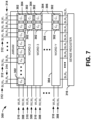
- the JMRAM memory cell circuit 50 is not limited to implementing a pair of Josephson junctions 54 and 56 in parallel with the PHMJJ 52, but could instead implement additional Josephson junctions or a single Josephson junction or could be configured as a variety of other arrangements. Accordingly, the JMRAM memory cell circuit 50 can be configured in a variety of ways.
- the JMRAM system 350 also includes additional word-read lines 364 for each of the rows 354 and additional bit-read lines 366 for each of the columns 356.
- the word-read line WLR 1 conducts a word-read current pulse I WR that passes through the 1 st row 354, including the JMRAM memory cells C X_1 and C 1_1 which selects the 1 st row 354 for reading.
- the word-read current I WR induces a current pulse from the primary windings L 1_1 and L 1_X , respectively, to the secondary windings L 2_1 and L 2_X , respectively.
- the bit-read lines BLR X and BLR 1 conduct bit-read currents I BR_X and I BR_1 , respectively, that pass through the X th and 1 st columns 356, including the JMRAM memory cells C X_1 and C 1_1 .
- the PHMJJs 358 provide a superconducting phase that affects the critical current of the Josephson junctions 360 and 362 depending on whether the PHMJJs 358 store a binary logic-1 state or a binary logic-0 state.
- the PHMJJ 358 associated with the JMRAM memory cell C X_1 provides a superconducting phase that generates a supercurrent that is added to the sense current I S_X through the Josephson junctions 360 and 362, similar to as demonstrated in the example of FIG. 5 .
- a sense register (not shown), such as the sense register 26 in the example of FIG. 7 , can monitor a voltage V X associated with the bit-read line BLR X and a voltage V 1 associated with the bit-read line BLR 1 .
- the sense register can compare the voltages V X and V 1 with a threshold, such as to perform differential voltage sensing.
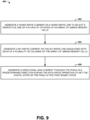
- FIG. 9 a methodology in accordance with various aspects of the present invention will be better appreciated with reference to FIG. 9 . While, for purposes of simplicity of explanation, the methodology of FIG. 9 is shown and described as executing serially, it is to be understood and appreciated that the present invention is not limited by the illustrated order, as some aspects could, in accordance with the present invention, occur in different orders and/or concurrently with other aspects from that shown and described herein.
- FIG. 9 illustrates an example of a method 400 for writing a digital state to a JMRAM memory cell (e.g., the JMRAM memory cell 10) in a JMRAM system (e.g., the JMRAM memory system 300) during a data write operation.
- a word-write current e.g., the word-write current I WW
- a word-write line e.g., the word-write line WLW
- select a respective one of a plurality of rows e.g., the rows 304) of an array of JMRAM memory cells.
- Each of the JMRAM memory cells includes a PHMJJ (e.g., the PHMJJ 12) that is magnetically coupled to the word-write line and to a bit-write line (e.g., the bit-write line BLW) and that is configured to store the digital state corresponding to one of a first binary state (e.g., logic-1) and a second binary state (e.g., logic-0).
- a bit-write current e.g., the bit-write current I BW
- a bit-write current I BW is generated on the bit-write line associated with each of a plurality of columns (e.g., the columns 306) of the array of JMRAM memory cells.
- the digital state of the PHMJJ is set in response to the word-write current and the bit-write current.
- a directional bias current (e.g., the directional bias current I D ) is generated through the PHMJJ in a predetermined direction during the data write operation to set the digital state of the PHMJJ in the first binary state.
- the directional bias current provides a superconducting phase (e.g., the current I ⁇ ) of the PHMJJ corresponding to the first binary state.
Landscapes
- Engineering & Computer Science (AREA)
- Computer Hardware Design (AREA)
- Superconductor Devices And Manufacturing Methods Thereof (AREA)
- Semiconductor Memories (AREA)
- Mram Or Spin Memory Techniques (AREA)
- Hall/Mr Elements (AREA)
Claims (15)
- Ein magnetischer Josephson-Speicher mit wahlfreiem Zugriff, im Folgenden JMRAM genannt, umfassend:eine Schreibschaltung, die so konfiguriert ist, dass sie während eines Datenschreibvorgangs Schreibströme (IWR, IRW , Iww) liefert;eine Leseschaltung, die so konfiguriert ist, dass sie einen Lesestrom (IR ) liefert; undeine JMRAM-Speicherzelle (10) mit:einen phasenhysteretischen magnetischen Josephson-Übergang, nachfolgend PHMJJ, (12, 52, 252), wobei der PHMJJ (12, 52, 252) äußere Schichten aus supraleitendem Material und eine oder mehrere Barriere(n) mit inneren Dünnfilmschichten aus ferromagnetischem Material enthält, die eine harte ferromagnetische Schicht mit einer im Wesentlichen festen Magnetisierung und eine weiche ferromagnetische Schicht umfassen, deren Magnetisierung als Ergebnis von Magnetfeldern schaltbar ist, die lokal durch zwei orthogonale elektrische Ströme (IRW , IWW ) der Schreibströme (IWR , IBW , IWW ) erzeugt werden;eine Leiterschleife;wobei der PHMJJ (12, 52, 252) so konfiguriert ist, dass er als Reaktion auf die Schreibströme, die während des Datenschreibvorgangs bereitgestellt werden, entweder einen ersten binären Zustand oder einen zweiten binären Zustand speichert, und wobei der PHMJJ (12, 52, 252) als Reaktion darauf, dass er sich im ersten binären Zustand befindet, so konfiguriert ist, dass er einen spontanen Überstrom in der Leiterschleife durch den PHMJJ (12, 52, 252) erzeugt;mindestens einen Josephson-Übergang (14, 56), der in der Leiterschleife angeordnet ist und einen kritischen Strom aufweist; wobei der kritische Strom so beschaffen ist, dass beim Bereitstellen des Lesestroms an den PHMJJ im ersten binären Zustand der Lesestrom mit dem spontanen Superstrom kombiniert wird, der von dem PHMJJ (12, 52, 252) im ersten binären Zustand erzeugt wird, um einen Strom mit einer Größe zu erzeugen, die größer ist als die des kritischen Stroms des mindestens einen Josephson-Übergangs;gekennzeichnet durchein Richtungsschreibelement (60, 262), das so konfiguriert ist, dass es während des Datenschreibvorgangs einen Richtungsvorspannungsstrom (ID ) auf der Grundlage eines der Schreibströme , IRW , IWW ) liefert, wobei der gerichtete Vorstrom (ID ) durch den PHMJJ fließt, um den PHMJJ zu zwingen, den spontanen Superstrom in eine vorbestimmte Richtung auszurichten, wenn der erste binäre Zustand während der Datenschreiboperation geschrieben wird, wobei die vorbestimmte Richtung des spontanen Superstroms die Richtung des Lesestroms (IR ) ist, wenn er durch den mindestens einen Josephson-Übergang fließt.
- Das JMRAM nach Anspruch 1, wobei das Richtungsschreibelement als mindestens ein Transformator (60) konfiguriert ist, der so konfiguriert ist, dass er den einen der Schreibströme von einer Primärwicklung zu einer Sekundärwicklung des mindestens einen Transformators (60) induktiv koppelt, um den Richtungsvorspannungsstrom durch den PHMJJ (12, 52, 252) in Reaktion auf den einen der Schreibströme während des Datenschreibvorgangs bereitzustellen.
- Das JMRAM nach Anspruch 1, wobei das Richtungsschreibelement als mindestens ein Transformator (60) konfiguriert ist, der eine Primärwicklung, die mit einer Bit-Schreibleitung oder einer Wort-Schreibleitung gekoppelt ist, auf der der eine der Schreibströme bereitgestellt wird, und eine Sekundärwicklung umfasst, die mit dem PHMJJ (12, 52, 252) in Reihe geschaltet ist, wobei der mindestens eine Transformator (60) so konfiguriert ist, dass er den einen der Schreibströme induktiv durch den PHMJJ (12, 52, 252) koppelt, um den Richtungsvorspannungsstrom für den PHMJJ (12, 52, 252) in Reaktion auf den einen der Schreibströme während des Datenschreibvorgangs bereitzustellen.
- Das JMRAM nach Anspruch 1, wobei die vorbestimmte Richtung einem positiven n-Zustand des PHMJJ (12, 52, 252) in Bezug auf die Richtung des Lesestroms während des Lesevorgangs entspricht.
- Das JMRAM nach Anspruch 1, wobei der PHMJJ (12, 52, 252) so konfiguriert ist, dass er den spontanen Superstrom als Reaktion auf das Speichern des ersten binären Zustands erzeugt, wobei der Lesestrom mit einem Superstrom kombiniert wird, der über die supraleitende Phase des PHMJJ (12, 52, 252) erzeugt wird, um den mindestens einen Josephson-Übergang auszulösen, um eine erste Größe einer Spannung an einem Ausgang der JMRAM-Speicherzelle (10) bereitzustellen, wobei die erste Größe der Spannung den ersten binären Zustand anzeigt.
- Das JMRAM nach Anspruch 5, wobei der PHMJJ (12, 52, 252) so konfiguriert ist, dass er als Reaktion auf das Speichern des zweiten binären Zustands keinen spontanen Superstrom erzeugt, so dass der mindestens eine Josephson-Übergang nicht triggert, so dass eine zweite Größe der Spannung am Ausgang bereitgestellt wird, wobei die zweite Größe der Spannung den zweiten binären Zustand anzeigt.
- Das JMRAM nach Anspruch 5, wobei der mindestens eine Josephson-Übergang als ein Paar von Josephson-Übergängen angeordnet ist, wobei als Reaktion darauf, dass der PHMJJ (12, 52, 252) den ersten binären Zustand speichert, der kombinierte Strom das Paar von Josephson-Übergängen in einer oszillierenden Weise triggert, um die erste Größe der Spannung am Ausgang bereitzustellen.
- Das JMRAM nach Anspruch 1, umfassend ein Array von JMRAM-Speicherzellen, das die JMRAM-Speicherzelle (10) umfasst, wobei das Array von JMRAM-Speicherzellen (10) in Zeilen und Spalten angeordnet ist und das JMRAM umfasst:eine Wort-Schreib-Leitung (WLW), die so konfiguriert ist, dass sie einen ersten (IWW ) der beiden orthogonalen elektrischen Ströme (IBW , IWW ) der Schreibströme als einen Wort-Schreib-Strom führt und mit einer Zeile des Arrays von JMRAM-Speicherzellen (10) verbunden ist;
eine Bit-Schreibleitung (BLW), die so konfiguriert ist, dass sie den zweiten (Isw) der beiden orthogonalen elektrischen Ströme (IBW , IWW ) der Schreibströme als einen BitSchreibstrom führt,eine Wort-Lese-Leitung (WLR), die mit der Zeile des Arrays von JMRAM-Speicherzellen (10) verbunden ist und so konfiguriert ist, dass sie den einen der Schreibströme während des Datenschreibvorgangs und während des Lesens als Wort-Lesestrom (IWR ) führt, undeine Bit-Leseleitung, die so konfiguriert ist, dass sie einen Bit-Lesestrom (IBR ) führt,wobei der Lesestrom (IR ) auf dem Wort-Lesestrom und dem Bit-Lesestrom basiert. - Das JMRAM nach Anspruch 8, wobei die Wort-Schreib-Leitung und die Bit-Schreib-Leitung, die mit der JMRAM-Speicherzelle (10) verbunden sind, magnetisch mit dem PHMJJ (12, 52, 252) gekoppelt sind.
- Das JMRAM nach Anspruch 8 umfasst ferner Bit-Leseleitungen, die jeweils einer der Spalten zugeordnet sind und so konfiguriert sind, dass sie Bit-Leseströme an die jeweiligen JMRAM-Speicherzellen (10) in einer gegebenen Zeile liefern, die in Reaktion auf den Wort-Lesestrom ausgewählt wird, der während eines Datenlesevorgangs geliefert wird, um eine Anzeige des gespeicherten digitalen Zustands jeder der JMRAM-Speicherzellen in der gegebenen Zeile auf der Vielzahl von Bit-Leseleitungen zu liefern.
- Ein Verfahren zum Schreiben eines digitalen Zustands in eine JMRAM-Speicherzelle (10) in einem Josephson-Magnet-Direktzugriffsspeicher, im folgenden (JMRAM) genannt, während einer Datenschreiboperation, wobei die JMRAM-Speicherzelle einen phasenhysteretischen magnetischen Josephson-Übergang, im folgenden PHMJJ genannt, (12, 52, 252), wobei der PHMJJ (12, 52, 252) äußere Schichten aus supraleitendem Material und eine oder mehrere Barrieren mit inneren Dünnfilmschichten aus ferromagnetischem Material umfasst, die eine hartferromagnetische Schicht mit einer im Wesentlichen festen Magnetisierung und eine weichferromagnetische Schicht umfassen, wobei der PHMJJ magnetisch mit einer Wort-Schreib-Leitung (WLW) und einer Bit-Schreib-Leitung (BLW) gekoppelt ist und so konfiguriert ist, dass er den digitalen Zustand speichert, der entweder einem ersten binären Zustand oder einem zweiten binären Zustand entspricht, wobei als Reaktion darauf, dass der PHMJJ (12, 52, 252) sich im ersten binären Zustand befindet, der PHMJJ (12, 52, 252) so konfiguriert ist, dass er einen spontanen Superstrom in einer Leiterschleife durch den PHMJJ (12, 52, 252) erzeugt; die JMRAM-Zelle ferner mindestens einen Josephson-Übergang (14, 56) umfasst, der in der Leiterschleife angeordnet ist und einen kritischen Strom aufweist, und das JMRAM ferner eine Leseschaltung umfasst, die so konfiguriert ist, dass sie einen Lesestrom (IR ) bereitstellt, wobei der kritische Strom derart ist, dass, wenn der Lesestrom an den PHMJJ im ersten binären Zustand bereitgestellt wird der Lesestrom mit dem von dem PHMJJ (2, 52, 252) in dem ersten binären Zustand erzeugten spontanen Superstrom kombiniert wird, um einen Strom mit einer Größe zu erzeugen, die größer ist als die des kritischen Stroms des mindestens einen Josephson-Übergangs, wobei das Verfahren umfasst:Erzeugen eines Wort-Schreib-Stroms (IWW ) auf der Wort-Schreib-Leitung (WLW), um die JMRAM-Speicherzelle auszuwählen;Erzeugen eines Bit-Schreib-Stroms (IBW ) auf der Bit-Schreib-Leitung, wobei der digitale Zustand des PHMJJ (12, 52, 252) in Reaktion auf den Wort-Schreib-Strom und den Bit-Schreib-Strom durch Schalten der Magnetisierung der weichferromagnetischen Schicht als Ergebnis des Anlegens von Magnetfeldern, die lokal durch den orthogonalen Wort-Schreib-Strom (IWW ) und den Bit-Schreib-Strom (IBW ) erzeugt werden, eingestellt wird;das Verfahren gekennzeichnet ist durch:
Erzeugen eines gerichteten Vorspannungsstroms (ID ) durch den PHMJJ (12, 52, 252) während des Datenschreibvorgangs, wobei der gerichtete Vorspannungsstrom (ID ) den PHMJJ zwingt, den spontanen Superstrom in eine vorbestimmte Richtung auszurichten, wenn der erste binäre Zustand der zu schreibende digitale Zustand ist, wobei die vorbestimmte Richtung des spontanen Superstroms die Richtung des Lesestroms (IR ) ist, wenn er durch den mindestens einen Josephson-Übergang fließt. - Das Verfahren nach Anspruch 11, wobei die Erzeugung des Richtungsvorstroms die Erzeugung des Richtungsvorstroms über mindestens einen Transformator (60) umfasst.
- Das Verfahren nach Anspruch 12, wobei das Erzeugen des Richtungsvorstroms über den mindestens einen Transformator (60) das Bereitstellen eines weiteren Schreibstroms (IWR ) durch eine Primärwicklung des mindestens einen Transformators (60) umfasst, wobei die Primärwicklung induktiv mit einer Sekundärwicklung des mindestens einen Transformators (60) gekoppelt ist, die Sekundärwicklung mit dem PHMJJ (12, 52, 252) gekoppelt ist, so dass der mindestens eine Transformator (60) den Richtungsvorspannungsstrom durch den PHMJJ (12, 52, 252) in Reaktion auf den Lesestrom während des Datenschreibvorgangs induziert.
- Das Verfahren nach Anspruch 12, wobei das Erzeugen des Richtungsvorstroms über den mindestens einen Transformator (262) das Bereitstellen des Wortschreibstroms oder des Bitschreibstroms durch eine Primärwicklung des mindestens einen Transformators (262) umfasst, wobei die Primärwicklung induktiv mit einer Sekundärwicklung des mindestens einen Transformators (262) gekoppelt ist, die Primärwicklung induktiv mit einer Sekundärwicklung des mindestens einen Transformators (262) gekoppelt ist, wobei die Sekundärwicklung in Reihe mit dem PHMJJ (12, 52, 252) angeordnet ist, so dass der mindestens eine Transformator (262) den gerichteten Vorspannungsstrom durch den PHMJJ (12, 52, 252) als Reaktion auf den jeweiligen Wortschreibstrom oder den Bitschreibstrom während des Datenschreibvorgangs induziert.
- Das Verfahren nach Anspruch 11, wobei das Erzeugen des gerichteten Vorstroms das Erzeugen des gerichteten Vorspannungsstroms umfasst, um den PHMJJ (12, 52, 252) in einen positiven n-Zustand zu versetzen, wenn der erste Binärzustand geschrieben werden soll, so dass der spontane Superstrom im Wesentlichen additiv zu mindestens einem von einem Wortlesestrom und einem Bitlesestrom ist, um den mindestens einen Josephson-Übergang auszulösen, um den ersten Binärzustand des PHMJJ (12, 52, 252) während eines Datenlesevorgangs anzuzeigen.
Applications Claiming Priority (2)
| Application Number | Priority Date | Filing Date | Title |
|---|---|---|---|
| US14/854,994 US9520181B1 (en) | 2015-09-15 | 2015-09-15 | Superconducting phase-controlled hysteretic magnetic Josephson junction JMRAM memory cell |
| PCT/US2016/048422 WO2017091258A2 (en) | 2015-09-15 | 2016-08-24 | Superconducting phase-controlled hysteretic magnetic josephson junction jmram memory cell |
Publications (2)
| Publication Number | Publication Date |
|---|---|
| EP3350808A2 EP3350808A2 (de) | 2018-07-25 |
| EP3350808B1 true EP3350808B1 (de) | 2023-05-03 |
Family
ID=57483818
Family Applications (1)
| Application Number | Title | Priority Date | Filing Date |
|---|---|---|---|
| EP16847602.6A Active EP3350808B1 (de) | 2015-09-15 | 2016-08-24 | Magnetische josephson-übergangsspeicherzelle und schreibschaltung |
Country Status (7)
| Country | Link |
|---|---|
| US (1) | US9520181B1 (de) |
| EP (1) | EP3350808B1 (de) |
| JP (1) | JP6507319B2 (de) |
| KR (1) | KR102081162B1 (de) |
| AU (1) | AU2016361158B2 (de) |
| CA (1) | CA2996621C (de) |
| WO (1) | WO2017091258A2 (de) |
Families Citing this family (16)
| Publication number | Priority date | Publication date | Assignee | Title |
|---|---|---|---|---|
| US10417136B2 (en) * | 2017-12-21 | 2019-09-17 | Northrop Grumman Systems Corporation | Write-through detection for a memory circuit with an analog bypass portion |
| US10204677B1 (en) * | 2018-03-16 | 2019-02-12 | Microsoft Technology Licensing, Llc | Superconducting memory system with stacked drivers and differential transformers |
| US10541024B2 (en) * | 2018-05-25 | 2020-01-21 | Microsoft Technology Licensing, Llc | Memory system with signals on read lines not phase-aligned with Josephson transmission line (JTL) elements included in the write lines |
| US10546621B2 (en) * | 2018-06-20 | 2020-01-28 | Microsoft Technology Licensing, Llc | Magnetic josephson junction driven flux-biased superconductor memory cell and methods |
| US10447278B1 (en) * | 2018-07-17 | 2019-10-15 | Northrop Grumman Systems Corporation | JTL-based superconducting logic arrays and FPGAs |
| US10650884B2 (en) * | 2018-09-04 | 2020-05-12 | Microsoft Technology Licensing, Llc | Superconducting memory with josephson phase-based torque |
| US10818346B2 (en) * | 2018-09-17 | 2020-10-27 | Northrop Grumman Systems Corporation | Quantizing loop memory cell system |
| US10923646B2 (en) | 2018-11-30 | 2021-02-16 | Microsoft Technology Licensing, Llc | Superconducting switch having a persistent and a non-persistent state |
| US11157804B2 (en) | 2019-01-25 | 2021-10-26 | Northrop Grumman Systems Corporation | Superconducting neuromorphic core |
| US10777263B1 (en) * | 2019-04-23 | 2020-09-15 | Northrop Grumman Systems Corporation | Josephson memory and logic circuits using quasi-long-junction interconnect |
| US11056634B1 (en) | 2019-12-16 | 2021-07-06 | Microsoft Technology Licensing, Llc | Josephson magnetic memory with a semiconductor-based magnetic spin valve |
| US11024791B1 (en) | 2020-01-27 | 2021-06-01 | Northrop Grumman Systems Corporation | Magnetically stabilized magnetic Josephson junction memory cell |
| US12080343B2 (en) * | 2021-10-28 | 2024-09-03 | William Robert Reohr | Read and write enhancements for arrays of superconducting magnetic memory cells |
| US12394454B2 (en) | 2021-11-24 | 2025-08-19 | William Robert Reohr | Time-division multiplexing for superconducting memory |
| CN119365925A (zh) * | 2022-03-23 | 2025-01-24 | 威廉·罗伯特·雷奥尔 | 用于将状态写入到具有集成的基于半导体的电路的超导电路中的方法和系统 |
| US20240212733A1 (en) * | 2022-12-22 | 2024-06-27 | William Robert Reohr | Methods and circuits for reading and writing pi-state-induced circulating currents into superconducting circuits containing magnetic josephson junctions |
Family Cites Families (4)
| Publication number | Priority date | Publication date | Assignee | Title |
|---|---|---|---|---|
| US6078517A (en) * | 1998-12-04 | 2000-06-20 | Trw Inc. | Superconducting memory cell with directly-coupled readout |
| US8270209B2 (en) * | 2010-04-30 | 2012-09-18 | Northrop Grumman Systems Corporation | Josephson magnetic random access memory system and method |
| US9013916B2 (en) * | 2012-05-31 | 2015-04-21 | Northrop Grumman Systems Corporation | Josephson magnetic memory cell system |
| US9208861B2 (en) * | 2013-10-01 | 2015-12-08 | Northrop Grumman Systems Corporation | Phase hysteretic magnetic Josephson junction memory cell |
-
2015
- 2015-09-15 US US14/854,994 patent/US9520181B1/en active Active
-
2016
- 2016-08-24 WO PCT/US2016/048422 patent/WO2017091258A2/en not_active Ceased
- 2016-08-24 KR KR1020187007511A patent/KR102081162B1/ko not_active Expired - Fee Related
- 2016-08-24 AU AU2016361158A patent/AU2016361158B2/en active Active
- 2016-08-24 EP EP16847602.6A patent/EP3350808B1/de active Active
- 2016-08-24 JP JP2018533039A patent/JP6507319B2/ja active Active
- 2016-08-24 CA CA2996621A patent/CA2996621C/en active Active
Also Published As
| Publication number | Publication date |
|---|---|
| EP3350808A2 (de) | 2018-07-25 |
| AU2016361158A1 (en) | 2018-03-22 |
| JP2018536250A (ja) | 2018-12-06 |
| AU2016361158B2 (en) | 2018-12-06 |
| CA2996621A1 (en) | 2017-06-01 |
| WO2017091258A3 (en) | 2017-08-10 |
| JP6507319B2 (ja) | 2019-04-24 |
| KR102081162B1 (ko) | 2020-02-25 |
| CA2996621C (en) | 2020-06-02 |
| WO2017091258A2 (en) | 2017-06-01 |
| KR20180048716A (ko) | 2018-05-10 |
| US9520181B1 (en) | 2016-12-13 |
Similar Documents
| Publication | Publication Date | Title |
|---|---|---|
| AU2016361158B2 (en) | Magnetic Josephson junction JMRAM memory cell and write circuit | |
| EP3053167B1 (de) | Phasenhysteretische magnetische josephson-übergangsspeicherzelle | |
| EP3268968B1 (de) | Phasenhysteretische magnetische josephson-übergangsspeicherzelle | |
| EP2564390B1 (de) | Josephson-magnetspeichersystem mit direktzugang und verfahren dafür | |
| JP7015964B2 (ja) | 量子化ループメモリセルシステム |
Legal Events
| Date | Code | Title | Description |
|---|---|---|---|
| STAA | Information on the status of an ep patent application or granted ep patent |
Free format text: STATUS: UNKNOWN |
|
| STAA | Information on the status of an ep patent application or granted ep patent |
Free format text: STATUS: THE INTERNATIONAL PUBLICATION HAS BEEN MADE |
|
| PUAI | Public reference made under article 153(3) epc to a published international application that has entered the european phase |
Free format text: ORIGINAL CODE: 0009012 |
|
| STAA | Information on the status of an ep patent application or granted ep patent |
Free format text: STATUS: REQUEST FOR EXAMINATION WAS MADE |
|
| 17P | Request for examination filed |
Effective date: 20180308 |
|
| AK | Designated contracting states |
Kind code of ref document: A2 Designated state(s): AL AT BE BG CH CY CZ DE DK EE ES FI FR GB GR HR HU IE IS IT LI LT LU LV MC MK MT NL NO PL PT RO RS SE SI SK SM TR |
|
| AX | Request for extension of the european patent |
Extension state: BA ME |
|
| DAV | Request for validation of the european patent (deleted) | ||
| DAX | Request for extension of the european patent (deleted) | ||
| STAA | Information on the status of an ep patent application or granted ep patent |
Free format text: STATUS: EXAMINATION IS IN PROGRESS |
|
| 17Q | First examination report despatched |
Effective date: 20191217 |
|
| GRAP | Despatch of communication of intention to grant a patent |
Free format text: ORIGINAL CODE: EPIDOSNIGR1 |
|
| STAA | Information on the status of an ep patent application or granted ep patent |
Free format text: STATUS: GRANT OF PATENT IS INTENDED |
|
| INTG | Intention to grant announced |
Effective date: 20221129 |
|
| GRAS | Grant fee paid |
Free format text: ORIGINAL CODE: EPIDOSNIGR3 |
|
| GRAA | (expected) grant |
Free format text: ORIGINAL CODE: 0009210 |
|
| STAA | Information on the status of an ep patent application or granted ep patent |
Free format text: STATUS: THE PATENT HAS BEEN GRANTED |
|
| AK | Designated contracting states |
Kind code of ref document: B1 Designated state(s): AL AT BE BG CH CY CZ DE DK EE ES FI FR GB GR HR HU IE IS IT LI LT LU LV MC MK MT NL NO PL PT RO RS SE SI SK SM TR |
|
| REG | Reference to a national code |
Ref country code: GB Ref legal event code: FG4D |
|
| REG | Reference to a national code |
Ref country code: DE Ref legal event code: R096 Ref document number: 602016079223 Country of ref document: DE |
|
| REG | Reference to a national code |
Ref country code: AT Ref legal event code: REF Ref document number: 1565360 Country of ref document: AT Kind code of ref document: T Effective date: 20230515 Ref country code: CH Ref legal event code: EP |
|
| REG | Reference to a national code |
Ref country code: IE Ref legal event code: FG4D |
|
| P01 | Opt-out of the competence of the unified patent court (upc) registered |
Effective date: 20230607 |
|
| REG | Reference to a national code |
Ref country code: NL Ref legal event code: FP |
|
| REG | Reference to a national code |
Ref country code: LT Ref legal event code: MG9D |
|
| REG | Reference to a national code |
Ref country code: AT Ref legal event code: MK05 Ref document number: 1565360 Country of ref document: AT Kind code of ref document: T Effective date: 20230503 |
|
| PG25 | Lapsed in a contracting state [announced via postgrant information from national office to epo] |
Ref country code: SE Free format text: LAPSE BECAUSE OF FAILURE TO SUBMIT A TRANSLATION OF THE DESCRIPTION OR TO PAY THE FEE WITHIN THE PRESCRIBED TIME-LIMIT Effective date: 20230503 Ref country code: PT Free format text: LAPSE BECAUSE OF FAILURE TO SUBMIT A TRANSLATION OF THE DESCRIPTION OR TO PAY THE FEE WITHIN THE PRESCRIBED TIME-LIMIT Effective date: 20230904 Ref country code: NO Free format text: LAPSE BECAUSE OF FAILURE TO SUBMIT A TRANSLATION OF THE DESCRIPTION OR TO PAY THE FEE WITHIN THE PRESCRIBED TIME-LIMIT Effective date: 20230803 Ref country code: ES Free format text: LAPSE BECAUSE OF FAILURE TO SUBMIT A TRANSLATION OF THE DESCRIPTION OR TO PAY THE FEE WITHIN THE PRESCRIBED TIME-LIMIT Effective date: 20230503 Ref country code: AT Free format text: LAPSE BECAUSE OF FAILURE TO SUBMIT A TRANSLATION OF THE DESCRIPTION OR TO PAY THE FEE WITHIN THE PRESCRIBED TIME-LIMIT Effective date: 20230503 |
|
| PG25 | Lapsed in a contracting state [announced via postgrant information from national office to epo] |
Ref country code: RS Free format text: LAPSE BECAUSE OF FAILURE TO SUBMIT A TRANSLATION OF THE DESCRIPTION OR TO PAY THE FEE WITHIN THE PRESCRIBED TIME-LIMIT Effective date: 20230503 Ref country code: PL Free format text: LAPSE BECAUSE OF FAILURE TO SUBMIT A TRANSLATION OF THE DESCRIPTION OR TO PAY THE FEE WITHIN THE PRESCRIBED TIME-LIMIT Effective date: 20230503 Ref country code: LV Free format text: LAPSE BECAUSE OF FAILURE TO SUBMIT A TRANSLATION OF THE DESCRIPTION OR TO PAY THE FEE WITHIN THE PRESCRIBED TIME-LIMIT Effective date: 20230503 Ref country code: LT Free format text: LAPSE BECAUSE OF FAILURE TO SUBMIT A TRANSLATION OF THE DESCRIPTION OR TO PAY THE FEE WITHIN THE PRESCRIBED TIME-LIMIT Effective date: 20230503 Ref country code: IS Free format text: LAPSE BECAUSE OF FAILURE TO SUBMIT A TRANSLATION OF THE DESCRIPTION OR TO PAY THE FEE WITHIN THE PRESCRIBED TIME-LIMIT Effective date: 20230903 Ref country code: HR Free format text: LAPSE BECAUSE OF FAILURE TO SUBMIT A TRANSLATION OF THE DESCRIPTION OR TO PAY THE FEE WITHIN THE PRESCRIBED TIME-LIMIT Effective date: 20230503 Ref country code: GR Free format text: LAPSE BECAUSE OF FAILURE TO SUBMIT A TRANSLATION OF THE DESCRIPTION OR TO PAY THE FEE WITHIN THE PRESCRIBED TIME-LIMIT Effective date: 20230804 |
|
| PG25 | Lapsed in a contracting state [announced via postgrant information from national office to epo] |
Ref country code: FI Free format text: LAPSE BECAUSE OF FAILURE TO SUBMIT A TRANSLATION OF THE DESCRIPTION OR TO PAY THE FEE WITHIN THE PRESCRIBED TIME-LIMIT Effective date: 20230503 |
|
| PG25 | Lapsed in a contracting state [announced via postgrant information from national office to epo] |
Ref country code: SK Free format text: LAPSE BECAUSE OF FAILURE TO SUBMIT A TRANSLATION OF THE DESCRIPTION OR TO PAY THE FEE WITHIN THE PRESCRIBED TIME-LIMIT Effective date: 20230503 |
|
| PG25 | Lapsed in a contracting state [announced via postgrant information from national office to epo] |
Ref country code: SM Free format text: LAPSE BECAUSE OF FAILURE TO SUBMIT A TRANSLATION OF THE DESCRIPTION OR TO PAY THE FEE WITHIN THE PRESCRIBED TIME-LIMIT Effective date: 20230503 Ref country code: SK Free format text: LAPSE BECAUSE OF FAILURE TO SUBMIT A TRANSLATION OF THE DESCRIPTION OR TO PAY THE FEE WITHIN THE PRESCRIBED TIME-LIMIT Effective date: 20230503 Ref country code: RO Free format text: LAPSE BECAUSE OF FAILURE TO SUBMIT A TRANSLATION OF THE DESCRIPTION OR TO PAY THE FEE WITHIN THE PRESCRIBED TIME-LIMIT Effective date: 20230503 Ref country code: EE Free format text: LAPSE BECAUSE OF FAILURE TO SUBMIT A TRANSLATION OF THE DESCRIPTION OR TO PAY THE FEE WITHIN THE PRESCRIBED TIME-LIMIT Effective date: 20230503 Ref country code: DK Free format text: LAPSE BECAUSE OF FAILURE TO SUBMIT A TRANSLATION OF THE DESCRIPTION OR TO PAY THE FEE WITHIN THE PRESCRIBED TIME-LIMIT Effective date: 20230503 Ref country code: CZ Free format text: LAPSE BECAUSE OF FAILURE TO SUBMIT A TRANSLATION OF THE DESCRIPTION OR TO PAY THE FEE WITHIN THE PRESCRIBED TIME-LIMIT Effective date: 20230503 |
|
| REG | Reference to a national code |
Ref country code: DE Ref legal event code: R097 Ref document number: 602016079223 Country of ref document: DE |
|
| PLBE | No opposition filed within time limit |
Free format text: ORIGINAL CODE: 0009261 |
|
| STAA | Information on the status of an ep patent application or granted ep patent |
Free format text: STATUS: NO OPPOSITION FILED WITHIN TIME LIMIT |
|
| PG25 | Lapsed in a contracting state [announced via postgrant information from national office to epo] |
Ref country code: MC Free format text: LAPSE BECAUSE OF FAILURE TO SUBMIT A TRANSLATION OF THE DESCRIPTION OR TO PAY THE FEE WITHIN THE PRESCRIBED TIME-LIMIT Effective date: 20230503 |
|
| REG | Reference to a national code |
Ref country code: CH Ref legal event code: PL |
|
| PG25 | Lapsed in a contracting state [announced via postgrant information from national office to epo] |
Ref country code: MC Free format text: LAPSE BECAUSE OF FAILURE TO SUBMIT A TRANSLATION OF THE DESCRIPTION OR TO PAY THE FEE WITHIN THE PRESCRIBED TIME-LIMIT Effective date: 20230503 |
|
| 26N | No opposition filed |
Effective date: 20240206 |
|
| PG25 | Lapsed in a contracting state [announced via postgrant information from national office to epo] |
Ref country code: LU Free format text: LAPSE BECAUSE OF NON-PAYMENT OF DUE FEES Effective date: 20230824 |
|
| PG25 | Lapsed in a contracting state [announced via postgrant information from national office to epo] |
Ref country code: LU Free format text: LAPSE BECAUSE OF NON-PAYMENT OF DUE FEES Effective date: 20230824 Ref country code: CH Free format text: LAPSE BECAUSE OF NON-PAYMENT OF DUE FEES Effective date: 20230831 |
|
| PG25 | Lapsed in a contracting state [announced via postgrant information from national office to epo] |
Ref country code: SI Free format text: LAPSE BECAUSE OF FAILURE TO SUBMIT A TRANSLATION OF THE DESCRIPTION OR TO PAY THE FEE WITHIN THE PRESCRIBED TIME-LIMIT Effective date: 20230503 |
|
| REG | Reference to a national code |
Ref country code: IE Ref legal event code: MM4A |
|
| PG25 | Lapsed in a contracting state [announced via postgrant information from national office to epo] |
Ref country code: SI Free format text: LAPSE BECAUSE OF FAILURE TO SUBMIT A TRANSLATION OF THE DESCRIPTION OR TO PAY THE FEE WITHIN THE PRESCRIBED TIME-LIMIT Effective date: 20230503 Ref country code: IT Free format text: LAPSE BECAUSE OF FAILURE TO SUBMIT A TRANSLATION OF THE DESCRIPTION OR TO PAY THE FEE WITHIN THE PRESCRIBED TIME-LIMIT Effective date: 20230503 |
|
| PG25 | Lapsed in a contracting state [announced via postgrant information from national office to epo] |
Ref country code: IE Free format text: LAPSE BECAUSE OF NON-PAYMENT OF DUE FEES Effective date: 20230824 |
|
| PG25 | Lapsed in a contracting state [announced via postgrant information from national office to epo] |
Ref country code: IE Free format text: LAPSE BECAUSE OF NON-PAYMENT OF DUE FEES Effective date: 20230824 Ref country code: FR Free format text: LAPSE BECAUSE OF NON-PAYMENT OF DUE FEES Effective date: 20230831 |
|
| PG25 | Lapsed in a contracting state [announced via postgrant information from national office to epo] |
Ref country code: BG Free format text: LAPSE BECAUSE OF FAILURE TO SUBMIT A TRANSLATION OF THE DESCRIPTION OR TO PAY THE FEE WITHIN THE PRESCRIBED TIME-LIMIT Effective date: 20230503 |
|
| PG25 | Lapsed in a contracting state [announced via postgrant information from national office to epo] |
Ref country code: BG Free format text: LAPSE BECAUSE OF FAILURE TO SUBMIT A TRANSLATION OF THE DESCRIPTION OR TO PAY THE FEE WITHIN THE PRESCRIBED TIME-LIMIT Effective date: 20230503 |
|
| PG25 | Lapsed in a contracting state [announced via postgrant information from national office to epo] |
Ref country code: CY Free format text: LAPSE BECAUSE OF FAILURE TO SUBMIT A TRANSLATION OF THE DESCRIPTION OR TO PAY THE FEE WITHIN THE PRESCRIBED TIME-LIMIT; INVALID AB INITIO Effective date: 20160824 |
|
| PG25 | Lapsed in a contracting state [announced via postgrant information from national office to epo] |
Ref country code: HU Free format text: LAPSE BECAUSE OF FAILURE TO SUBMIT A TRANSLATION OF THE DESCRIPTION OR TO PAY THE FEE WITHIN THE PRESCRIBED TIME-LIMIT; INVALID AB INITIO Effective date: 20160824 |
|
| PGFP | Annual fee paid to national office [announced via postgrant information from national office to epo] |
Ref country code: NL Payment date: 20250821 Year of fee payment: 10 |
|
| PGFP | Annual fee paid to national office [announced via postgrant information from national office to epo] |
Ref country code: DE Payment date: 20250820 Year of fee payment: 10 |
|
| PGFP | Annual fee paid to national office [announced via postgrant information from national office to epo] |
Ref country code: BE Payment date: 20250820 Year of fee payment: 10 Ref country code: GB Payment date: 20250821 Year of fee payment: 10 |
|
| PG25 | Lapsed in a contracting state [announced via postgrant information from national office to epo] |
Ref country code: TR Free format text: LAPSE BECAUSE OF FAILURE TO SUBMIT A TRANSLATION OF THE DESCRIPTION OR TO PAY THE FEE WITHIN THE PRESCRIBED TIME-LIMIT Effective date: 20230503 |