EP3053167B1 - Phasenhysteretische magnetische josephson-übergangsspeicherzelle - Google Patents
Phasenhysteretische magnetische josephson-übergangsspeicherzelle Download PDFInfo
- Publication number
- EP3053167B1 EP3053167B1 EP14747479.5A EP14747479A EP3053167B1 EP 3053167 B1 EP3053167 B1 EP 3053167B1 EP 14747479 A EP14747479 A EP 14747479A EP 3053167 B1 EP3053167 B1 EP 3053167B1
- Authority
- EP
- European Patent Office
- Prior art keywords
- read
- current
- bit
- memory cells
- word
- Prior art date
- Legal status (The legal status is an assumption and is not a legal conclusion. Google has not performed a legal analysis and makes no representation as to the accuracy of the status listed.)
- Active
Links
Images


Classifications
-
- G—PHYSICS
- G11—INFORMATION STORAGE
- G11C—STATIC STORES
- G11C11/00—Digital stores characterised by the use of particular electric or magnetic storage elements; Storage elements therefor
- G11C11/21—Digital stores characterised by the use of particular electric or magnetic storage elements; Storage elements therefor using electric elements
- G11C11/44—Digital stores characterised by the use of particular electric or magnetic storage elements; Storage elements therefor using electric elements using super-conductive elements, e.g. cryotron
-
- B—PERFORMING OPERATIONS; TRANSPORTING
- B82—NANOTECHNOLOGY
- B82Y—SPECIFIC USES OR APPLICATIONS OF NANOSTRUCTURES; MEASUREMENT OR ANALYSIS OF NANOSTRUCTURES; MANUFACTURE OR TREATMENT OF NANOSTRUCTURES
- B82Y10/00—Nanotechnology for information processing, storage or transmission, e.g. quantum computing or single electron logic
-
- G—PHYSICS
- G01—MEASURING; TESTING
- G01R—MEASURING ELECTRIC VARIABLES; MEASURING MAGNETIC VARIABLES
- G01R33/00—Arrangements or instruments for measuring magnetic variables
- G01R33/02—Measuring direction or magnitude of magnetic fields or magnetic flux
- G01R33/035—Measuring direction or magnitude of magnetic fields or magnetic flux using superconductive devices
- G01R33/0354—SQUIDS
-
- G—PHYSICS
- G01—MEASURING; TESTING
- G01R—MEASURING ELECTRIC VARIABLES; MEASURING MAGNETIC VARIABLES
- G01R33/00—Arrangements or instruments for measuring magnetic variables
- G01R33/02—Measuring direction or magnitude of magnetic fields or magnetic flux
- G01R33/035—Measuring direction or magnitude of magnetic fields or magnetic flux using superconductive devices
- G01R33/0354—SQUIDS
- G01R33/0358—SQUIDS coupling the flux to the SQUID
-
- G—PHYSICS
- G11—INFORMATION STORAGE
- G11C—STATIC STORES
- G11C11/00—Digital stores characterised by the use of particular electric or magnetic storage elements; Storage elements therefor
- G11C11/02—Digital stores characterised by the use of particular electric or magnetic storage elements; Storage elements therefor using magnetic elements
- G11C11/14—Digital stores characterised by the use of particular electric or magnetic storage elements; Storage elements therefor using magnetic elements using thin-film elements
- G11C11/15—Digital stores characterised by the use of particular electric or magnetic storage elements; Storage elements therefor using magnetic elements using thin-film elements using multiple magnetic layers
-
- G—PHYSICS
- G11—INFORMATION STORAGE
- G11C—STATIC STORES
- G11C11/00—Digital stores characterised by the use of particular electric or magnetic storage elements; Storage elements therefor
- G11C11/02—Digital stores characterised by the use of particular electric or magnetic storage elements; Storage elements therefor using magnetic elements
- G11C11/16—Digital stores characterised by the use of particular electric or magnetic storage elements; Storage elements therefor using magnetic elements using elements in which the storage effect is based on magnetic spin effect
- G11C11/165—Auxiliary circuits
- G11C11/1653—Address circuits or decoders
- G11C11/1655—Bit-line or column circuits
-
- G—PHYSICS
- G11—INFORMATION STORAGE
- G11C—STATIC STORES
- G11C11/00—Digital stores characterised by the use of particular electric or magnetic storage elements; Storage elements therefor
- G11C11/02—Digital stores characterised by the use of particular electric or magnetic storage elements; Storage elements therefor using magnetic elements
- G11C11/16—Digital stores characterised by the use of particular electric or magnetic storage elements; Storage elements therefor using magnetic elements using elements in which the storage effect is based on magnetic spin effect
- G11C11/165—Auxiliary circuits
- G11C11/1653—Address circuits or decoders
- G11C11/1657—Word-line or row circuits
-
- G—PHYSICS
- G11—INFORMATION STORAGE
- G11C—STATIC STORES
- G11C11/00—Digital stores characterised by the use of particular electric or magnetic storage elements; Storage elements therefor
- G11C11/02—Digital stores characterised by the use of particular electric or magnetic storage elements; Storage elements therefor using magnetic elements
- G11C11/16—Digital stores characterised by the use of particular electric or magnetic storage elements; Storage elements therefor using magnetic elements using elements in which the storage effect is based on magnetic spin effect
- G11C11/165—Auxiliary circuits
- G11C11/1659—Cell access
-
- G—PHYSICS
- G11—INFORMATION STORAGE
- G11C—STATIC STORES
- G11C11/00—Digital stores characterised by the use of particular electric or magnetic storage elements; Storage elements therefor
- G11C11/02—Digital stores characterised by the use of particular electric or magnetic storage elements; Storage elements therefor using magnetic elements
- G11C11/16—Digital stores characterised by the use of particular electric or magnetic storage elements; Storage elements therefor using magnetic elements using elements in which the storage effect is based on magnetic spin effect
- G11C11/165—Auxiliary circuits
- G11C11/1673—Reading or sensing circuits or methods
-
- G—PHYSICS
- G11—INFORMATION STORAGE
- G11C—STATIC STORES
- G11C11/00—Digital stores characterised by the use of particular electric or magnetic storage elements; Storage elements therefor
- G11C11/02—Digital stores characterised by the use of particular electric or magnetic storage elements; Storage elements therefor using magnetic elements
- G11C11/16—Digital stores characterised by the use of particular electric or magnetic storage elements; Storage elements therefor using magnetic elements using elements in which the storage effect is based on magnetic spin effect
- G11C11/165—Auxiliary circuits
- G11C11/1675—Writing or programming circuits or methods
-
- H—ELECTRICITY
- H10—SEMICONDUCTOR DEVICES; ELECTRIC SOLID-STATE DEVICES NOT OTHERWISE PROVIDED FOR
- H10N—ELECTRIC SOLID-STATE DEVICES NOT OTHERWISE PROVIDED FOR
- H10N60/00—Superconducting devices
- H10N60/10—Junction-based devices
- H10N60/12—Josephson-effect devices
-
- H—ELECTRICITY
- H10—SEMICONDUCTOR DEVICES; ELECTRIC SOLID-STATE DEVICES NOT OTHERWISE PROVIDED FOR
- H10N—ELECTRIC SOLID-STATE DEVICES NOT OTHERWISE PROVIDED FOR
- H10N60/00—Superconducting devices
- H10N60/80—Constructional details
- H10N60/805—Constructional details for Josephson-effect devices
-
- H—ELECTRICITY
- H10—SEMICONDUCTOR DEVICES; ELECTRIC SOLID-STATE DEVICES NOT OTHERWISE PROVIDED FOR
- H10N—ELECTRIC SOLID-STATE DEVICES NOT OTHERWISE PROVIDED FOR
- H10N69/00—Integrated devices, or assemblies of multiple devices, comprising at least one superconducting element covered by group H10N60/00
Definitions
- the present invention relates generally to quantum and classical digital superconducting circuits, and specifically to a phase hysteretic magnetic Josephson junction memory cell.
- Superconducting digital technology has provided computing and/or communications resources that benefit from unprecedented high speed, low power dissipation, and low operating temperature.
- superconducting digital technology has lacked random-access memory (RAM) with adequate capacity and speed relative to logic circuits. This has been a major obstacle to industrialization for current applications of superconducting technology in telecommunications and signal intelligence, and can be especially forbidding for high-end and quantum computing. All concepts currently considered for superconducting memory have been based on quantization of magnetic flux quanta in a superconducting inductive loop.
- CMOS complementary metal-oxide semiconductor
- CMOS complementary metal-oxide semiconductor
- One hybrid memory solution has been proposed where the memory core implements CMOS technology and the bit-line detection is done with Josephson devices.
- CMOS complementary metal-oxide semiconductor
- US 2012/184445 A1 refers to a superconducting memory cell which includes a magnetic Josephson junction (MJJ) with a ferromagnetic material and has at least two switchable states of magnetization.
- MJJ magnetic Josephson junction
- Magnetic Josephson Junctions with Superconducting Interlayer for Cryogenic Memory refers to a superconducting device with ferromagnetic barrier for a scalable high-density cryogenic memory compatible with energy-efficient single flux quantum (SFQ) circuits.
- SFQ single flux quantum
- the memory cell includes a phase hysteretic magnetic Josephson junction (PHMJJ) that is configured to store one of a first binary logic state corresponding to a binary logic-1 state and a second binary logic state corresponding to a binary logic-0 state in response to a first write current and a second write current and to generate a superconducting phase based on the stored digital state.
- the memory cell also includes at least one Josephson junction having a critical current that is based on the superconducting phase of the PHMJJ and being configured to provide an output corresponding to the stored digital state in response to a first read current and a second read current.
- Another aspect of the present invention includes a method for reading a JMRAM .
- the method includes generating a word-read current on a word-read line to select a respective one of a plurality of rows of an array of memory cells, each of the memory cells comprising a phase hysteretic magnetic Josephson junction (PHMJJ ) that is configured to store a digital state corresponding to one of a binary logic-1 state and a binary logic-0 state.
- the method also includes generating a bit-read current on a bit-read line associated with each of a plurality of columns of the array of memory cells.
- PHMJJ phase hysteretic magnetic Josephson junction
- the method further includes reading the digital state from each of the memory cells in the respective one of the plurality of rows based on whether at least one Josephson junction in the respective memory cells triggers in response to the word-read current and the bit-read current associated with each of the plurality of columns of the array of memory cells based on a superconducting phase provided by the PHMJJ corresponding to the stored digital state.
- the memory array includes a plurality of word-write lines each configured to conduct a respective word-write current that selects a given row of memory cells during a data write operation.
- Each of the memory cells includes a PHMJJ .
- the memory array also includes a plurality of bit-write lines each configured to conduct a respective bit-write current to write a digital state corresponding to one of a binary logic-0 state and a binary logic-1 state into the PHMJJ associated with each memory cell of the given row of memory cells.
- the PHMJJ can be magnetically coupled to a respective one of the plurality of word-write lines and a respective one of the plurality of bit-write lines.
- the memory array also includes a plurality of word-read lines each configured to conduct a respective word-read current that selects a given row of memory cells during a data read operation.
- the memory array further includes a plurality of bit-read lines each configured to conduct a respective bit-read current through each of the memory cells in a given column, the at least one Josephson junction providing an indication of the stored digital state during the data read operation in response to the word-read current, the bit-read current, and a superconducting phase provided by the PHMJJ corresponding to the stored digital state.
- the present invention relates generally to quantum and classical digital superconducting circuits, and specifically to a phase hysteretic magnetic Josephson junction memory cell.
- the JMRAM system can implement an array of memory cells that each includes a phase hysteretic magnetic Josephson junction ( PHMJJ ) that can be configured as including ferromagnetic materials in an associated barrier.
- the memory cells can also each include at least one Josephson junction (e.g., a pair of Josephson junctions in parallel with the PHMJJ ).
- the PHMJJ can be configured to store a digital state corresponding to one of a binary logic-1 state or a binary logic-0 state in response to a word-write current and a bit-write current associated with the PHMJJ .
- the word-write and bit-write currents can each be provided on dedicated word-write and bit-write lines, and can set the logic state of the PHMJJ based on respective current flow directions relative to each other.
- the PHMJJ of each of the memory cells of the array can provide an indication of the stored digital state in response to a word-read current and a bit-read current.
- the PHMJJ can be configured as a switchable ⁇ -junction that is configured to generate a superconducting phase based on the digital state stored therein. The superconducting phase can thus lower a critical current associated with the at least one Josephson junction of each of the memory cells of a row of the array.
- the word-read current and the bit-read current can be provided to trigger the Josephson junction(s) to change a voltage on the associated bit-read line based on the PHMJJ storing a digital state corresponding to a binary logic-1 state, and to not trigger based on the PHMJJ storing a digital state corresponding to a binary logic-0 state.
- the bit-read line can have a voltage having a magnitude that varies based on whether the digital state of the PHMJJ corresponds to the binary logic-1 state or the binary logic-0 state (e.g., between a zero and a non-zero amplitude).
- the term "trigger" with respect to Josephson junctions describes the phenomenon of the Josephson junction generating a discrete voltage pulse in response to a current flow through the Josephson junction exceeding a critical current.
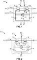
- FIG. 1 illustrates an example of a memory cell 10 in accordance with an aspect of the invention.
- the memory cell 10 can correspond to one of a plurality of memory cells that are arranged in an array as rows and columns, as described in greater detail herein.
- the memory cell 10 includes a first write line WLW and a first read line WLR that each pass through the memory cell 10.
- the first write line WLW conducts a first write current I WW during a data write operation and the first read line WLR conducts a first read current I WR during a data read operation.
- the first write current I WW can correspond to a word-write current associated with a row of memory cells in an array
- the first read current I WR can correspond to a word-read current associated with the row of memory cells in the array.
- the first write and first read lines WLW and WLR can likewise be coupled to adjacent memory cells in a given row on either side of the memory cell 10.
- the first read and first write currents I WW and I WR flow through all of the memory cell systems in the row, including the memory cell 10, during the respective data write and data read operations.
- the memory cell 10 includes a second write line BLW and a second read line BLR that each pass through the memory cell 10.
- the second write line BLW conducts a second write current I BW during the data write operation and the second read line BLR conducts a second read current I BR during the data read operation.
- the second write current I BW can correspond to a bit-write current associated with a column of memory cells in the array
- the first read current I BR can correspond to a bit-read current associated with the column of memory cells in the array.
- the second write and second read lines BLW and BLR can likewise be coupled to adjacent memory cells in a given column above and below the memory cell 10.
- the second read and second write currents I BW and I BR flow through all of the memory cell systems in the column, including the memory cell 10, during the respective data write and data read operations.
- the memory cell 10 also includes a phase hysteretic magnetic Josephson junction (PHMJJ ) 12 that is configured to store a digital state corresponding to one of the binary logic-1 state or the binary logic-0 state.
- the PHMJJ 12 can include ferromagnetic materials in associated barriers to be configured as a switchable ⁇ -junction.
- the memory cell 10 also includes a first Josephson junction 14 and a second Josephson junction 16 that are arranged in parallel with the PHMJJ 12.
- the Josephson junctions 14 and 16 can be configured as superconductor-ferromagnetic-superconductor (SFS) Josephson junctions.
- FSS superconductor-ferromagnetic-superconductor
- the PHMJJ 12 can include outer layers of superconducting material, such as Niobium (Nb), and one or more internal thin film layers of ferromagnetic materials.
- the thin film layers of ferromagnetic materials can include one or more "hard” ferromagnetic layers having a substantially fixed magnetic field and one or more "soft” ferromagnetic layers that can be changed as a result of magnetic fields generated locally by orthogonal electrical currents.
- the PHMJJ 12 can include one or more additional layers, such as oxide layers, that are interleaved with the superconducting and/or ferromagnetic layers.
- the first write line WLW and the second write line BLW are demonstrated as magnetically coupled to the PHMJJ 12, as indicated at 16.
- the PHMJJ 12 can include two or more different ferromagnetic layers, and the orientation of the magnetic field in one of the ferromagnetic layers is substantially fixed. The magnetic field orientation of the other one or more ferromagnetic layers can be changed as a result of magnetic fields that are generated locally by the first write current I WW and the second write current I BW .
- the first write current I WW and the second write current I BW can generate the magnetic field to set the digital state of the PHMJJ 12 to a binary logic-1 state or a binary logic-0 state using magneto-current states of the PHMJJ 12 based on the respective directions of current flow during a data write operation.
- the individual magnetic fields of each of the first write current I WW and the second write current I BW can add together positively or negatively to set the digital state of the phase hysteretic magnetic Josephson junction to correspond to a binary logic-1 state or a binary logic-0 state respectively.
- the digital state of the PHMJJ 12 remains unchanged.
- the first write current I WW and the second write current I BW can be applied as a sequence of write current pulses, such that if the first write current pulse I WW overlaps in time with the second write current pulse I BW , the digital state of the PHMJJ 12 can correspond to a binary logic-1 state or a binary logic-0 state. However, if only one such pulse is present at a given time, or if the first and the second write current pulses I WW and I BW do not sufficiently overlap in time, the digital state of the PHMJJ 12 can remain unchanged.
- the individual magnetic field of only one of the first write current I WW and the second write current I BW may be insufficient to change the digital state of the PHMJJ 12, such that memory cells in unaddressed rows maintain their respective digital states despite the flow of the second write current I BW .
- cross coupling between the first write line WLW and the second write line BLW can be substantially mitigated.
- the current-flow directions of the respective second write currents I BW in each of the columns can be controlled to set the digital state of each of the PHMJJs 12 in a given row during a data write operation without affecting the digital states in any of the memory cells in any of the other rows through which a first write current I WW is not provided.
- the memory cell 10 includes a first transformer 18 and a second transformer 20 that are arranged in series with respect to each other.
- the first transformer 18 includes a primary winding L 1 and the second transformer 20 includes a primary winding L 3 that are arranged in series on the first read line WLR through which the first read current I WR flows.
- the first transformer 18 also includes a secondary winding L 2 inductively coupled to the primary winding L 1 and the second transformer 20 also includes a secondary winding L 4 inductively coupled to the primary winding L 3 .
- the secondary windings L 2 and L 4 are collectively arranged in parallel with the PHMJJ 12 and in parallel with the Josephson junctions 14 and 16.
- the first read current I WR is inductively provided to the Josephson junctions 14 and 16, as described in greater detail herein.
- the first read current I WR being provided to the Josephson junctions 14 and 16 can refer to the first read current I WR being provided to the Josephson junctions 14 and 16 directly or inductively, as described in the example of FIG. 1 .
- the second read line BLR is coupled to a node 22 between the secondary windings L 2 and L 4 , such that the second read current I BR enters the memory cell 10 at the node 22, and is coupled to a node 24 corresponding to an output of the memory cell 10 between the Josephson junctions 14 and 16, such that the second read current I BR exits the memory cell 10 from the node 24.
- the digital state of the PHMJJ 12 can be read from the memory cell 10 in response to the first read current I WR and the second read current I BR .
- the first read current I WR can be provided on the first read line WLR to select the row of memory cells in the associated memory array.
- the first read current I WR flows through the primary windings L 1 and L 3 of the respective transformers 18 and 20 as a DC current pulse.
- the DC current pulse of the first read current I WR is inductively provided to the PHMJJ 12 and the Josephson junctions 14 and 16.
- the second read current I BR is provided between the secondary windings L 2 and L 4 .
- the current induced by the first read current I WR via the secondary windings L 2 and L 4 is added to second read current I BR based on the direction of current flow of the first read current I WR .
- the stored binary digital state of the PHMJJ 12 can be determinative of the critical current necessary to trigger the Josephson junctions 14 and 16 based on the superconducting phase that can be provided by the PHMJJ 12.
- the PHMJJ 12 is in a zero state, and thus stores a logic-0 binary state, the PHMJJ 12 is in a substantially minimum Josephson energy ground state that does not provide superconducting phase. Therefore, the added magnitude of the second read current I BR and the first read current I WR , as induced to the Josephson junctions 14 and 16, is not sufficient to trigger the Josephson junctions 14 and 16. Accordingly, a voltage on the second read line BLR can remain at a substantially decreased magnitude (e.g., zero volts) to indicate the logic-0 state.
- the PHMJJ 12 if the PHMJJ 12 is in a ⁇ -state, and thus stores a logic-1 binary state, the PHMJJ 12 has a substantially maximum Josephson energy and provides a superconducting phase that is added to the magnitude of the second read current I BR and the first read current I WR .
- the term "superconducting phase" corresponds to a spontaneous supercurrent circulating in a loop through the PHMJJ 12 and the Josephson junctions 14 and 16 in response to the PHMJJ 12 being in the ⁇ -state, with the supercurrent having a magnitude based on an internal superconductor flux quantum divided by a mutual inductance term.
- the Josephson junctions 14 and 16 can trigger in an oscillatory manner to increase the voltage on the second read line BLR to indicate the logic-1 state.
- FIG. 2 illustrates an example of a diagram 50 of readout of the memory cell 10.
- the memory cell 10 is demonstrated in the example of FIG. 2 as excluding the second write line BLW and the first write line WLW for simplicity.
- the PHMJJ 12 is in a zero state, and thus stores a logic-0 binary state.
- the PHMJJ 12 provides a magnitude zero superconducting phase (i.e., no superconducting phase).
- the first read current I WR flows through the primary windings L 1 and L 3 of the respective transformers 18 and 20 (e.g., as a DC current pulse), and is thus inductively provided to the PHMJJ 12 and the Josephson junctions 14 and 16. Additionally, the second read current I BR is provided to the memory cell 10 between the secondary windings L 2 and L 4 . Therefore, the current induced by the first read current I WR via the secondary windings L 2 and L 4 is added to second read current I BR based on the direction of current flow of the first read current I WR . In the example of FIG.
- the induced first read current I WR and the second read current I BR are combined to provide a first current loop I 1 that flows through the PHMJJ 12 and the secondary windings L 2 and L 4 and a second current loop I 2 that flows through the Josephson junctions 14 and 16 and the secondary windings L 2 and L 4 . Because the PHMJJ 12 does not provide any superconducting phase, a portion of both the induced first read current I WR and the second read current I BR flows through the PHMJJ 12 (i.e., the current loop I 1 in the example of FIG. 2 ).
- this portion of both the induced first read current I WR and the second read current I BR that flows through the PHMJJ 12 is diverted away from flowing through the Josephson junctions 14 and 16, leaving only the portion of the current loop I 2 as a sense current flowing through the Josephson junctions 14 and 16.
- the current loop I 2 can thus have a magnitude that is less than the critical current of the Josephson junctions 14 and 16, and is thus insufficient to trigger the Josephson junctions 14 and 16. Accordingly, a voltage that is measured on the second read line BLR maintains a substantially lesser magnitude (e.g., zero volts) to indicate the logic-0 binary state that is stored in the PHMJJ 12.
- FIG. 3 illustrates another example of a diagram 100 of readout of the memory cell 10. Similar to as described previously in the example of FIG. 2 , the memory cell 10 is demonstrated in the example of FIG. 3 as excluding the second write line BLW and the first write line WLW for simplicity.
- the PHMJJ 12 is in a ⁇ -state, and thus stores a logic-1 binary state.
- the PHMJJ 12 provides a superconducting phase that is demonstrated diagrammatically as a current I ⁇ .
- the induced first read current I WR is added to second read current I BR based on the direction of current flow of the first read current I WR .
- the PHMJJ 12 is in the ⁇ -state, and thus produces the superconducting phase demonstrated by the current I ⁇ , the combined induced first read current I WR and second read current I BR are suppressed from flowing through the PHMJJ 12 from the secondary winding L 4 . Therefore, substantially all of the combined induced first read current I WR and second read current I BR flows through the Josephson junction 14. In the example of FIG.
- the induced first read current I WR , the second read current I BR , and the superconducting phase current In are combined to provide a first current loop I 3 that flows through the PHMJJ 12 and the Josephson junctions 14 and 16 and a second current loop I 4 that flows through the Josephson junctions 14 and 16 and the secondary windings L 2 and L 4 .
- the first current loop I 3 can correspond to the current In flowing as a supercurrent loop through the PHMJJ 12 and the Josephson junctions 14 and 16
- the second current loop I 4 can correspond to a sum of the first read current I WR and second read current I BR .
- the combined first and second current loops I 3 and I 4 can have a magnitude that is greater than the critical current of the Josephson junction 14, and is thus sufficient to trigger the Josephson junction 14.
- the Josephson junction 14 can trigger to generate a voltage pulse on the second read line BLR.
- the triggering of the Josephson junction 14 can thus cause the Josephson junction 16 to trigger, which can thus continue to provide sequential triggering between the Josephson junctions 14 and 16 in an oscillatory manner to substantially maintain the voltage pulses on the second read line BLR.
- the substantially increased voltage provided by the voltage pulses on the second read line BLR can indicate the logic-1 binary state that is stored in the PHMJJ 12.
- the memory cell 10 is not intended to be limited to the example of FIGS. 1 through 3 .
- the memory cell 10 is demonstrated diagrammatically, such that the arrangement of the first lines WLR and WLW and the second lines BLR and BLW with respect to each other and to the PHMJJ 12 can vary.
- the configuration of the first write line WLW and the second write line BLW can be such that the direction of current flow of the first write current I WW and the second write current I BW can be opposite to store the digital state in the PHMJJ 12.
- the memory cell 10 is not limited to implementing a pair of Josephson junctions 14 and 16 in parallel with the PHMJJ 12, but could instead implement additional Josephson junctions or a single Josephson junction or could be configured as a variety of other arrangements. Accordingly, the memory cell 10 can be configured in a variety of ways.
- FIG. 4 illustrates an example of a Josephson magnetic random access memory (JMRAM) system 150 in accordance with an aspect of the invention.
- the JMRAM system 150 can be implemented as a memory structure in a variety of computing applications.
- the JMRAM system 150 is demonstrated in the example of FIG. 4 as being arranged as an array of memory cells 152.
- the memory cells 152 are arranged in rows 154 that each correspond to a data word, demonstrated as WORD 1 through WORD Y, where Y is an integer greater than 1.
- Each of the rows 154 includes a set of memory cells 152 that form X columns 156 across the rows 154, with the memory cells 152 in WORD 1 being demonstrated in the example of FIG. 4 as C 1 to C X , where X is an integer greater than 1. Therefore, each of the memory cells 152 in the array of the JMRAM system 150 can be individually addressable by row 154 and column 156.
- each of the rows 154 is demonstrated as having an associated word-write line 158 and word-read line 160, demonstrated as WLW 1 and WLR 1 through WLW Y and WLR Y , respectively.
- the word-write line 158 and word-read line 160 can be inductively and/or magnetically coupled to each of the memory cells 152 in each of the rows 154 of the JMRAM system 150.
- each of the memory cells 152 is demonstrated as having an associated bit-write line 162 and bit-read line 164, demonstrated as BLW 1 and BLR 1 through BLW Y and BLRy, respectively.
- the bit-write line 162 and bit-read line 164 can be coupled to each corresponding numbered memory cell 152 in each of the rows 154 of the JMRAM system 150, such that the memory cells 152 in each column 156 are arranged in series with respect to the bit-write line 162 and bit-read line 164.
- FIG. 4 describes that the word-write lines 158 and word-read lines 160 and the bit-write lines 162 and bit-read lines 164 are arranged in series with other adjacent memory cells in the respective row and column, the word-write lines 158 and word-read lines 160 and the bit-write lines 162 and bit-read lines 164 could instead be dedicated with respect to each memory cell 152.
- Each of the memory cells 152 is configured to store a single bit of data.
- each of the memory cells 152 can include at least one phase hysteretic magnetic Josephson junction that can be configured to store a digital state corresponding to a binary logic-1 or a binary logic-0.
- the digital state can be set in response to a word-write current that is provided on the respective word-write line 158 and a bit-write current that is provided on the respective bit-write line 162.
- the respective digital state that is stored in each of the memory cells 152 can be read from the memory cells 152 based on a word-read current that is provided on the respective word-read line 160 to select a given one of the rows 154 and a bit-read current that is provided on the respective bit-read line 164.
- the bit-read line 164 of each of the columns 156 is coupled to a sense register 166 that is configured to measure the respective bit-read line 164 to determine whether digital state of each of the memory cells 152 of an associated row 154 correspond to a binary logic-1 state or a binary logic-0 state in response to the word-read current and the bit-read current during a data read operation.
- the sense register 166 can measure a voltage or a current associated with the bit-read line 164, as described in greater detail herein.
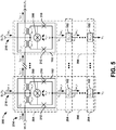
- FIG. 5 illustrates another example of a JMRAM system 200 in accordance with an aspect of the invention.
- the JMRAM system 200 can be configured similar to the JMRAM system 200 in the example of FIG. 4 .
- FIG. 4 in the following description of the example of FIG. 5 .
- FIG. 5 demonstrates a data read operation in which data is read from the JMRAM system 200.
- the JMRAM system 200 is demonstrated in the example of FIG. 5 as being arranged as an array of memory cells 202.
- the memory cells 202 are arranged in rows 204 that each correspond to a data WORD 1 through Y, where Y is an integer greater than 1.
- Each of the rows 204 includes a set of memory cells 202 that form X columns 206 across the rows 204, where X is an integer greater than 1.
- each of the demonstrated memory cells 202 is designated by column and row, from C 1_1 to C X_Y .
- the memory cells 202 corresponding to memory cells C 1_1 and C X_1 are demonstrated in greater detail.
- the memory cells C 1_1 and C X_1 include first and second transformers that include primary windings L 1_1 and L 3_1 and L 1_X and L 3_X , respectively, and secondary windings L 2_1 and L 4_1 and L 2_X and L 4_X , respectively.
- the memory cells C 1_1 and C X_1 also each include a PHMJJ 208 in parallel with a pair of Josephson junctions 210 and 212. It is to be understood that the memory cells C 1_1 and C X_1 can also include word-write and bit-write lines, similar to as demonstrated in the example of FIG. 4 , but have been omitted from the example of FIG. 5 for brevity.
- the JMRAM system 200 also includes a word-read line 214, demonstrated as WLR 1 , thus corresponding to the 1 st row 204, which passes through the primary windings L 1_X and L 3_X and L 1_1 and L 3_1 of the memory cells C X_1 and C 1_1 , respectively.
- the JMRAM system 200 also includes bit-read lines 216, demonstrated as BLR X and BLR 1 , thus corresponding to the X th and 1 st columns 206, respectively.
- the bit-read lines 216 are demonstrated as coupled to the PHMJJs 208. It is to be understood that, while the example of FIG.
- the JMRAM system 200 also includes additional word-read lines 214 for each of the rows 204 and additional bit-read lines 216 for each of the columns 206.
- the word-read line WLR 1 conducts a DC word-read current pulse I WR that passes through the 1 st row 204, including the memory cells C X_1 and C 1_1 which selects the 1 st row 204 for reading.
- the word-read current I WR induces a DC current pulse from the primary windings L 1_1 and L 3_1 and L 1_X and L 3_X , respectively, to the secondary windings L 2_1 and L 4_1 and L 2_X and L 4_X , respectively.
- bit-read lines BLR X and BLR 1 conduct bit-read currents I BR_X and I BR_1 , respectively, that pass through the X th and 1 st columns 206, including the memory cells C X_1 and C 1_1 .
- the collective current of the word-read current I WR and the bit-read currents I BR_X and I BR_1 through the Josephson junctions 210 and 212 are demonstrated collectively in the memory cells C X_1 and C 1_1 as sense currents I S_X and I S_1 , respectively.
- the PHMJJ 208 that is associated with the memory cell C X_1 is demonstrated as storing a binary logic-1 state ('1') and the PHMJJ 208 that is associated with the memory cell C 1_1 is demonstrated as storing a binary logic-0 state ('0').
- the digital states of the memory cells C X_1 and C 1_1 could have been set in a previously performed data write operation. Similar to as described above in the example of FIG.
- the PHMJJs 208 can provide a superconducting phase that affects the critical current of the Josephson junctions 210 and 212 depending on whether the PHMJJs 208 store a binary logic-1 state or a binary logic-0 state.
- the PHMJJ 208 associated with the memory cell C X_1 can provide a superconducting phase that is added to the sense current I S_X through the Josephson junctions 210 and 212, similar to as demonstrated in the example of FIG. 3 .
- the PHMJJ 208 associated with the memory cell C 1_1 can provide a zero superconducting phase, such that the sense current I S_1 through the Josephson junctions 210 and 212 is based on a portion of the added magnitudes of the word-read current I WR and the bit-read current I BR_1 , similar to as demonstrated in the example of FIG. 2 .
- a sense register (not shown), such as the sense register 26 in the example of FIG. 4 , can monitor a voltage V X associated with the bit-read line BLR X and a voltage V 1 associated with the bit-read line BLR 1 .
- the sense register can compare the voltages V X and V 1 with a threshold, such as to perform differential voltage sensing.
- the Josephson junctions 210 and 212 upon triggering, can provide a voltage pulse, such that the voltage V X can have a magnitude that is greater than the voltage V 1 . Accordingly, in the example of FIG. 5 , the greater magnitude of the voltage V X and the lesser magnitude of the voltage V 1 , such as relative to a threshold magnitude, can indicate that the memory cell C X_1 stores a binary logic-1 state and the memory cell C 1_1 stores a binary logic-0 state.
- the associated sense register can be configured to measure a magnitude of the bit-read currents I BR_X and I BR_1 to determine the digital state of the respective memory cells C X_1 and C 1_1 .
- bit-read currents can be provided for all of the columns 206 therebetween, such that associated voltages on the respective bit-read lines 216 can be monitored in a similar manner. Accordingly, the entire data word associated with the 1 st row 204 can be concurrently read during the data read operation. In this manner, the memory cells 202 in any of the rows 204 can be read during the data read operation, as described in the example of FIG. 5 .
- FIG. 6 a methodology in accordance with various aspects of the present invention will be better appreciated with reference to FIG. 6 . While, for purposes of simplicity of explanation, the methodology of FIG. 6 is shown and described as executing serially, it is to be understood and appreciated that the present invention is not limited by the illustrated order, as some aspects could, in accordance with the present invention, occur in different orders and/or concurrently with other aspects from that shown and described herein. Moreover, not all illustrated features may be required to implement a methodology in accordance with an aspect of the present invention.
- FIG. 6 illustrates an example of a method 250 for reading a memory cell in a JMRAM system (e.g., the JMRAM system 150).
- a word-read current (e.g., the word-read current I WR ) is generated on a word-read line (e.g., the word-read line WLR) to select a respective one of a plurality of rows (e.g., the rows 154) of an array of memory cells (e.g., the memory cells 152), each of the memory cells comprising a PHMJJ (e.g., the PHMJJ 52) that is configured to store a digital state corresponding to one of a binary logic-1 state and a binary logic-0 state.
- a PHMJJ e.g., the PHMJJ 52
- bit-read current (e.g., the bit-read current I BR ) is generated on a bit-read line (e.g., the bit-read line BLR) associated with each of a plurality of columns (e.g., the columns 156) of the array of memory cells.
- the digital state is read from each of the memory cells in the respective one of the plurality of rows based on whether at least one Josephson junction (e.g., the Josephson junctions 54 and 56) in the respective memory cells triggers in response to the word-read current and the bit-read current associated with each of the plurality of columns of the array of memory cells based on a superconducting phase (e.g., the current I ⁇ ) provided by the PHMJJ corresponding to the stored digital state.
- a superconducting phase e.g., the current I ⁇
Landscapes
- Engineering & Computer Science (AREA)
- Computer Hardware Design (AREA)
- Physics & Mathematics (AREA)
- General Physics & Mathematics (AREA)
- Condensed Matter Physics & Semiconductors (AREA)
- Nanotechnology (AREA)
- Chemical & Material Sciences (AREA)
- Mathematical Physics (AREA)
- Crystallography & Structural Chemistry (AREA)
- Theoretical Computer Science (AREA)
- Superconductor Devices And Manufacturing Methods Thereof (AREA)
- Semiconductor Memories (AREA)
- Mram Or Spin Memory Techniques (AREA)
Claims (15)
- Speicherzelle (10), aufweisend:einen phasenhysteretischen magnetischen Josephson-Kontakt (12), MJJ, der zum Speichern entweder eines ersten binären logischen Zustands entsprechend einem Binär-Logik-1-Zustand oder eines zweiten binären logischen Zustands entsprechend einem Binär-Logik-O-Zustand als Reaktion auf einen Schreibstrom (Iww, IBW) und zum Generieren einer supraleitenden Phase (In) auf Basis des gespeicherten digitalen Zustands konfiguriert ist; undmindestens einen Josephson-Kontakt (14, 16) mit einem auf der supraleitenden Phase (In) des phasenhysteretischen magnetischen MJJ (12) basierenden kritischen Strom und dazu konfiguriert, einen Ausgang entsprechend dem gespeicherten digitalen Zustand als Reaktion auf einen Lesestrom (IWR, IBR) bereitzustellen,dadurch gekennzeichnet, dassdie supraleitende Phase (In) des phasenhysteretischen magnetischen MJJ (12) einen spontanen Suprastrom generiert, der in einer Schleife durch den phasenhysteretischen MJJ (12) und den mindestens einen Josephson-Kontakt (14, 16) zirkuliert.
- Speicherzelle nach Anspruch 1, wobei der phasenhysteretische MJJ (12) zum Generieren der supraleitenden Phase (In) als Reaktion auf die Speicherung entweder des ersten binären logischen Zustands oder des zweiten binären logischen Zustands konfiguriert ist, wobei sich der Lesestrom (IWR, IBR) mit der supraleitenden Phase (In) des phasenhysteretischen MJJ (12) vereinigt, um den mindestens einen Josephson-Kontakt (14, 16) zum Bereitstellen einer Spannung mit einer ersten Größe an einem Ausgang der Speicherzelle auszulösen, wobei die erste Größe der Spannung entweder den ersten binären logischen Zustand oder den zweiten binären logischen Zustand angibt.
- Speicherzelle nach Anspruch 2, wobei der phasenhysteretische MJJ (12) zum Generieren einer nullsupraleitenden Phase (In) als Reaktion auf die Speicherung des anderen von entweder des ersten binären logischen Zustands oder des zweiten binären logischen Zustands konfiguriert ist, wobei der vereinigte Lesestrom (IWR, IBR) und die supraleitende Phase (In) des phasenhysteretischen MJJ (12) den mindestens einen Josephson-Kontakt (14, 16) nicht auszulösen, so dass eine Spannung mit einer zweiten Größe am Ausgang bereitgestellt wird, wobei die zweite Größe der Spannung den anderen des entweder ersten binären logischen Zustands oder es zweiten binären logischen Zustands angibt.
- Speicherzelle nach Anspruch 2, wobei der mindestens eine Josephson-Kontakt (14, 16) als ein Paar Josephson-Kontakte angeordnet ist, wobei als Reaktion auf den entweder eines des ersten oder des zweiten binären logischen Zustands speichernden phasenhysteretischen MJJ (12) der Lesestrom (IWR, IBR) das Paar Josephson-Kontakte (14, 16) auf eine oszillatorische Weise auslöst, um die Spannung mit der ersten Größe aufrechtzuerhalten, während der Lesestrom (IWR, IBR) bereitgestellt wird.
- Speicherzelle nach Anspruch 1, die ferner mindestens einen Transformator (18, 20) aufweist, der zum induktiven Koppeln des Lesestroms (IWR, IBR) aus einer Primärwicklung (L1, L3) mit einer Sekundärwicklung (L2, L4) des mindestens einen Transformators (18, 20) konfiguriert ist, um den Lesestrom (IWR, IBR) dem phasenhysteretischen MJJ (12) und dem mindestens einen Josephson-Kontakt (14, 16) bereitzustellen.
- Speicherzelle nach Anspruch 5, wobei der mindestens eine Josephson-Kontakt (14, 16) als ein Paar Josephson-Kontakte parallel zu einer sekundären Wicklung (L2, L4) des mindestens einen Transformators (18, 20) und parallel zum phasenhysteretischen MJJ (12) angeordnet ist, wobei der Lesestrom (IWR, IBR) ein erster Lesestrom (IWR) ist, wobei ein zweiter Lesestrom (IBR) der Speicherzelle zwischen der Sekundärwicklung (L2, L4) des mindestens einen Transformators (18, 20) bereitgestellt wird, der zweite Lesestrom (IBR) sich mit dem ersten Lesestrom (IWR), der über den mindestens einen Transformator induziert wird, und mit der supraleitenden Phase (In) vereinigt, um das Paar Josephson-Kontakte (14, 16) als Reaktion auf den phasenhysteretischen MJJ (12), der entweder einen des ersten binären logischen Zustands oder des zweiten binären logischen Zustands speichert, auszulösen und das Paar Josephson-Kontakte (14, 16) als Reaktion auf den phasenhysteretischen MJJ (12), der den anderen entweder des ersten binären logischen Zustands oder des zweiten binären logischen Zustands speichert, nicht auszulösen.
- Magnetisches Josephson-Arbeitsspeichersystem, JMRAM, (150), das ein Array von Speicherzellen (152) mit der Speicherzelle (10) von Anspruch 1 aufweist, wobei das Array der Speicherzellen (152) Reihen (154) und Spalten (156) umfasst, wobei der Schreibstrom (IWW) ein Wort-Schreibstrom ist, der über eine einer Reihe (154) des Array der Speicherzellen (152) zugehörigen Wort-Schreibleitung (WLW) bereitgestellt wird, wobei ein zweiter Schreibstrom (IBW) über eine Bit-Schreibleitung (BLW) des Array der Speicherzellen (152) als ein Bit-Schreibstrom bereitgestellt wird, wobei der Lesestrom (IWR) ein Lesestrom (IWR) ist, der über eine einer Reihe (154) des Array der Speicherzellen (152) zugehörigen Wort-Leseleitung (WLR) bereitgestellt wird, und wobei ein zweiter Lesestrom (IBR) über eine Bit-Leseleitung (BLR) als ein Bit-Lesestrom bereitgestellt wird.
- JMRAM (150) nach Anspruch 7, wobei die Wort-Schreibleitung (WLW) und die Wort-Lese-leitung (WLR) jeder der Speicherzellen einer gegebenen Reihe (154) des Array (156) gemeinsam sind, und wobei die Bit-Schreibleitung (BLW) und die Bit-Leseleitung (BLR) jeder der Speicherzellen in einer gegebenen Spalte (156) des Array (152) gemeinsam sind, so dass das Array der Speicherzellen bezüglich jeder Reihe und jeder Spalte des Array seriell angeordnet ist.
- JMRAM (150) nach Anspruch 7, wobei jede Wort-Schreibleitung (WLW) und die Bit-Schreibleitung (BLW), die einer gegebenen Speicherzelle zugehörig sind, mit dem phasenhysteretischen MJJ (12) magnetisch gekoppelt ist, wobei der Wort-Schreibstrom (Iww) durch jede der Speicherzellen in einer gegeben Reihe (154) während einer Datenschreiboperation über die Wort-Schreibleitung (WLW) bereitgestellt wird, und wobei die Bit-Schreibleitung (BLW) eine Mehrzahl Bit-Schreibleitungen aufweist, die jeweils einer entsprechenden der Spalten (156) zugehörig sind, wobei jeder einer entsprechenden Mehrzahl Bit-Schreibströme (IBW) eine Stromrichtung hat, die der Speicherung entweder des binären Logik-1-Zustands oder des binären Logik-O-Zustands in jeder der Speicherzellen in der gegebenen Reihe (154) entspricht.
- JMRAM (150) nach Anspruch 7, wobei die Bit-Leseleitung (BLR) eine Mehrzahl Bit-Leseleitungen (BLR) aufweist, die jeweils einer entsprechenden der Spalten (156) zugehörig sind, wobei jeder einer entsprechenden Mehrzahl Bit-Schreibströme (IBW) dem mindestens einen Josephson-Kontakt (14, 16) bereitgestellt wird, der jeder der entsprechenden Speicherzellen in einer gegebenen Reihe (154) zugehörig ist, die als Reaktion auf den Wort-Lesestrom (IWR) während einer Datenleseoperation gewählt wird, um eine Angabe über den gespeicherten digital Zustand jedes der phasenhysteretischen MJJ (12) in der gegebenen Reihe (154) der Mehrzahl Bit-Leseleitungen bereitzustellen.
- Verfahren zum Lesen einer Speicherzelle (10) in einem magnetischen Josephson-Speichersystem mit wahlfreiem Zugriff, JMRAM, (150), wobei das Verfahren aufweist:Generieren (252) eines Wort-Lesestroms (IwR) in einer Wort-Leseleitung (WLR), um eine entsprechende Reihe aus einer Mehrzahl Reihen (154) eines Array von Speicherzellen (152) zu wählen, wobei jede der Speicherzellen einen phasenhysteretischen magnetischen Josephson-Kontakt , MJJ, (12) aufweist, der zum Speichern eines digitalen Zustands entsprechend entweder einem binären Logik-1-Zustand oder einem binären Logik-0-Zustand konfiguriert ist;Generieren (254) eines Bit-Lesestroms (IBR) in einer jeder Spalte einer Mehrzahl Spalten (156) des Array von Speicherzellen (152) zugehörigen Bit-Leseleitung (BLR); undLesen (256) des digitalen Zustands aus jeder der Speicherzellen in der entsprechenden Reihe der Mehrzahl Reihen (154) in Abhängigkeit davon, ob mindestens ein Josephson-Kontakt (14, 16) in den entsprechenden Speicherzellen auslöst als Reaktion auf den Wort-Lesestrom (IWR) und den Bit-Lesestrom (IBR), die jeder Spalte der Mehrzahl Spalten (156) des Arry von Speicherzellen zugehörig sind, auf Basis einer supraleitenden Phase (In), die vom phasenhysteretischen MJJ (12) entsprechenden dem gespeicherten digitalen Zustand bereitgestellt wird,dadurch gekennzeichnet, dass
die supraleitende Phase des phasenhysteretischen magnetischen MJJ (12) einen spontanen Suprastrom generiert, der in einer Schleife durch den phasenhysteretischen MJJ (12) und den mindestens einen Josephson-Kontakt (14, 16) zirkuliert: - Verfahren nach Anspruch 11, wobei das Lesen des digitalen Zustands das Messen entweder einer Spannung oder eines Stroms der jeder Spalte der Mehrzahl Spalten (156) eines Array von Speicherzellen (152) zugehörigen Bit-Leseleitung (BLR) aufweist, wobei eine Größe entweder der Spannung oder des Stroms angibt, ob der mindestens eine Josephson-Kontakt (14, 16) der Speicherzellen in der entsprechenden Reihe der Mehrzahl Reihen (154) als Reaktion auf den Wort-Lesestrom (IWR) und den Bit-Lesestrom (IBR), die jeder Spalte der Mehrzahl Spalten (156) des Array von Speicherzellen zugehörig sind, auslöst.
- Verfahren nach Anspruch 11, wobei das serielle Generieren des Wort-Lesestroms (IWR) das Bereitstellen des Wort-Lesestroms (IWR) in der Wort-Leseleitung (WLR) in jeder Speicherzelle in der entsprechenden Reihe der Mehrzahl Reihen (154) aufweist, und wobei das Generieren des Bit-Lesestroms (IBR) das Bereitstellen des Bit-Lesestroms (IBR) in der Bit-Leseleitung (BLR) durch jede der Speicherzellen in jeder Speicherzelle der Mehrzahl Speicherzellen in jeder Spalte der Mehrzahl Spalten (156) aufweist.
- Verfahren nach Anspruch 11, wobei das Lesen des Zustands aus jeder der Speicherzellen aufweist:Auslösen des mindesten einen Josephson-Kontakts (14, 16) als Reaktion auf das Bereitstellen einer supraleitenden Phase (In) durch den phasenhysteretischen MJJ (12), die zum Bit-Lesestrom (IBR) und zum Wort-Lesestrom (IWR) auf Basis des vom phasenhysteretischen MJJ (12) gespeicherten binären Logik-1-Zustands oder des binären Logik-O-Zustands addiert wird; undNichtauslösen des mindesten einen Josephson-Kontakts (14, 16) als Reaktion auf das Nichtbereitstellen einer supraleitenden Phase (In) durch den phasenhysteretischen MJJ (12) auf Basis des vom phasenhysteretischen MJJ (12) gespeicherten binären Logik-1-Zustands oder des binären Logik-O-Zustands.
- Verfahren nach Anspruch 11, ferner aufweisend:Bereitstellen des Wort-Lesestroms (IWR), der jeder Speicherzelle der Speicherzellen in der entsprechenden Reihe der Mehrzahl Reihen (154) zugehörig ist, über einen ersten Transformator (18) und einen zweiten Transformator (20), die zum induktiven Bereitstellen des Wort-Lesestroms (IWR) an den mindestens einen Josephson-Kontakt (14, 16) konfiguriert sind;Generieren eines Messstroms, der die Summe aus den Wort-Lesestrom, dem Bit-Lesestrom und der supraleitenden Phase ist, die auf dem im phasenhysteretischen MJJ (12) gespeicherten digitalen Zustand basiert; undAuslösen eines Paares Josephson-Kontakte (14, 16) auf oszillatorische Weise, wenn der Messstrom einen dem Paar Josephson-Kontakte (14, 16) zugehörigen kritischen Strom überschreitet.
Applications Claiming Priority (2)
| Application Number | Priority Date | Filing Date | Title |
|---|---|---|---|
| US14/043,360 US9208861B2 (en) | 2013-10-01 | 2013-10-01 | Phase hysteretic magnetic Josephson junction memory cell |
| PCT/US2014/046886 WO2015050621A1 (en) | 2013-10-01 | 2014-07-16 | Phase hysteretic magnetic josephson junction memory cell |
Publications (2)
| Publication Number | Publication Date |
|---|---|
| EP3053167A1 EP3053167A1 (de) | 2016-08-10 |
| EP3053167B1 true EP3053167B1 (de) | 2020-05-06 |
Family
ID=51265860
Family Applications (1)
| Application Number | Title | Priority Date | Filing Date |
|---|---|---|---|
| EP14747479.5A Active EP3053167B1 (de) | 2013-10-01 | 2014-07-16 | Phasenhysteretische magnetische josephson-übergangsspeicherzelle |
Country Status (7)
| Country | Link |
|---|---|
| US (1) | US9208861B2 (de) |
| EP (1) | EP3053167B1 (de) |
| JP (1) | JP6159881B2 (de) |
| KR (1) | KR101902444B1 (de) |
| AU (1) | AU2014329991B2 (de) |
| CA (1) | CA2925848C (de) |
| WO (1) | WO2015050621A1 (de) |
Families Citing this family (41)
| Publication number | Priority date | Publication date | Assignee | Title |
|---|---|---|---|---|
| US9355364B2 (en) * | 2014-03-10 | 2016-05-31 | Northrop Grumman Systems Corporation | Reciprocal quantum logic comparator for qubit readout |
| US10650319B2 (en) | 2015-02-06 | 2020-05-12 | Northrop Grumman Systems Corporation | Flux control of qubit under resonant excitation |
| US9384827B1 (en) | 2015-03-05 | 2016-07-05 | Northrop Grumman Systems Corporation | Timing control in a quantum memory system |
| US9281057B1 (en) | 2015-03-11 | 2016-03-08 | Northrop Grumman Systems Corporation | Phase hysteretic magnetic Josephson junction memory cell |
| US9520181B1 (en) * | 2015-09-15 | 2016-12-13 | Northrop Grumman Systems Corporation | Superconducting phase-controlled hysteretic magnetic Josephson junction JMRAM memory cell |
| US9443576B1 (en) * | 2015-11-09 | 2016-09-13 | Microsoft Technology Licensing, Llc | Josephson magnetic random access memory with an inductive-shunt |
| US10122350B2 (en) | 2015-11-17 | 2018-11-06 | Northrop Grumman Systems Corporation | Josephson transmission line (JTL) system |
| US9595970B1 (en) * | 2016-03-24 | 2017-03-14 | Northrop Grumman Systems Corporation | Superconducting cell array logic circuit system |
| US9613699B1 (en) * | 2016-04-22 | 2017-04-04 | Microsoft Technology Licensing, Llc | Memory system with a content addressable superconducting memory |
| US9972380B2 (en) * | 2016-07-24 | 2018-05-15 | Microsoft Technology Licensing, Llc | Memory cell having a magnetic Josephson junction device with a doped magnetic layer |
| US9779803B1 (en) * | 2017-03-01 | 2017-10-03 | Northrop Grumman Systems Corporation | Memory circuit with write-bypass portion |
| US11211722B2 (en) | 2017-03-09 | 2021-12-28 | Microsoft Technology Licensing, Llc | Superconductor interconnect system |
| US10608157B2 (en) | 2017-05-18 | 2020-03-31 | International Business Machines Corporation | Qubit network non-volatile identification |
| US10826713B2 (en) | 2017-05-18 | 2020-11-03 | International Business Machines Corporation | Qubit network secure identification |
| US10122351B1 (en) | 2017-07-25 | 2018-11-06 | Northrop Grumman Systems Corporation | Superconducting bi-directional current driver |
| US10491178B2 (en) | 2017-10-31 | 2019-11-26 | Northrop Grumman Systems Corporation | Parametric amplifier system |
| US10756712B2 (en) | 2017-11-13 | 2020-08-25 | Northrop Grumman Systems Corporation | RQL phase-mode flip-flop |
| WO2019096416A1 (en) | 2017-11-18 | 2019-05-23 | Universiteit Leiden | Hybrid superconducting-ferromagnet random access memory element |
| US10417136B2 (en) * | 2017-12-21 | 2019-09-17 | Northrop Grumman Systems Corporation | Write-through detection for a memory circuit with an analog bypass portion |
| US10204677B1 (en) | 2018-03-16 | 2019-02-12 | Microsoft Technology Licensing, Llc | Superconducting memory system with stacked drivers and differential transformers |
| US10122352B1 (en) | 2018-05-07 | 2018-11-06 | Northrop Grumman Systems Corporation | Current driver system |
| US10546621B2 (en) | 2018-06-20 | 2020-01-28 | Microsoft Technology Licensing, Llc | Magnetic josephson junction driven flux-biased superconductor memory cell and methods |
| US10447278B1 (en) | 2018-07-17 | 2019-10-15 | Northrop Grumman Systems Corporation | JTL-based superconducting logic arrays and FPGAs |
| US10554207B1 (en) | 2018-07-31 | 2020-02-04 | Northrop Grumman Systems Corporation | Superconducting non-destructive readout circuits |
| US10615783B2 (en) | 2018-07-31 | 2020-04-07 | Northrop Grumman Systems Corporation | RQL D flip-flops |
| US10650884B2 (en) * | 2018-09-04 | 2020-05-12 | Microsoft Technology Licensing, Llc | Superconducting memory with josephson phase-based torque |
| US10818346B2 (en) | 2018-09-17 | 2020-10-27 | Northrop Grumman Systems Corporation | Quantizing loop memory cell system |
| US10587245B1 (en) * | 2018-11-13 | 2020-03-10 | Northrop Grumman Systems Corporation | Superconducting transmission line driver system |
| US11211117B2 (en) | 2019-01-24 | 2021-12-28 | Northrop Grumman Systems Corporation | Ferrimagnetic/ferromagnetic exchange bilayers for use as a fixed magnetic layer in a superconducting-based memory device |
| US10885974B2 (en) | 2019-01-30 | 2021-01-05 | Northrop Grumman Systems Corporation | Superconducting switch |
| US10879447B2 (en) | 2019-03-13 | 2020-12-29 | Northrop Grumman Systems Corporation | Repeating alternating multilayer buffer layer |
| US11024791B1 (en) | 2020-01-27 | 2021-06-01 | Northrop Grumman Systems Corporation | Magnetically stabilized magnetic Josephson junction memory cell |
| US11545288B2 (en) | 2020-04-15 | 2023-01-03 | Northrop Grumman Systems Corporation | Superconducting current control system |
| US11201608B2 (en) | 2020-04-24 | 2021-12-14 | Northrop Grumman Systems Corporation | Superconducting latch system |
| US11342491B2 (en) | 2020-09-28 | 2022-05-24 | Northrop Grumman Systems Corporation | Magnetic Josephson junction system |
| US11444233B1 (en) | 2021-03-31 | 2022-09-13 | Northrop Grumman Systems Corporation | Josephson magnetic memory cell with ferrimagnetic layers having orthogonal magnetic polarity |
| AU2022289736A1 (en) | 2021-06-11 | 2024-02-01 | Caleb JORDAN | System and method of flux bias for superconducting quantum circuits |
| US11757467B2 (en) | 2021-08-13 | 2023-09-12 | Northrop Grumman Systems Corporation | Circuits for converting SFQ-based RZ and NRZ signaling to bilevel voltage NRZ signaling |
| US12597925B2 (en) | 2022-12-08 | 2026-04-07 | Northrop Grumman Systems Corporation | Superconducting current control system |
| US20240212733A1 (en) * | 2022-12-22 | 2024-06-27 | William Robert Reohr | Methods and circuits for reading and writing pi-state-induced circulating currents into superconducting circuits containing magnetic josephson junctions |
| US12395140B2 (en) | 2023-07-27 | 2025-08-19 | Northrop Grumman Systems Corporation | Non-return to zero (NRZ) amplifier system |
Family Cites Families (6)
| Publication number | Priority date | Publication date | Assignee | Title |
|---|---|---|---|---|
| US4601015A (en) * | 1982-02-23 | 1986-07-15 | Nippon Electric Co., Ltd. | Josephson memory circuit |
| JPH05190922A (ja) * | 1992-01-09 | 1993-07-30 | Hitachi Ltd | 量子メモリ装置 |
| US8670807B2 (en) | 2007-08-21 | 2014-03-11 | D-Wave Systems Inc. | Systems, methods, and apparatus for controlling the elements of superconducting processors |
| US8208288B2 (en) | 2008-03-27 | 2012-06-26 | International Business Machines Corporation | Hybrid superconducting-magnetic memory cell and array |
| US8270209B2 (en) * | 2010-04-30 | 2012-09-18 | Northrop Grumman Systems Corporation | Josephson magnetic random access memory system and method |
| US8971977B2 (en) | 2011-01-17 | 2015-03-03 | Hypres, Inc. | Superconducting devices with ferromagnetic barrier junctions |
-
2013
- 2013-10-01 US US14/043,360 patent/US9208861B2/en active Active
-
2014
- 2014-07-16 EP EP14747479.5A patent/EP3053167B1/de active Active
- 2014-07-16 CA CA2925848A patent/CA2925848C/en active Active
- 2014-07-16 WO PCT/US2014/046886 patent/WO2015050621A1/en not_active Ceased
- 2014-07-16 AU AU2014329991A patent/AU2014329991B2/en active Active
- 2014-07-16 KR KR1020167011128A patent/KR101902444B1/ko active Active
- 2014-07-16 JP JP2016519936A patent/JP6159881B2/ja active Active
Non-Patent Citations (1)
| Title |
|---|
| None * |
Also Published As
| Publication number | Publication date |
|---|---|
| CA2925848C (en) | 2018-07-03 |
| AU2014329991A1 (en) | 2016-04-21 |
| JP6159881B2 (ja) | 2017-07-05 |
| US20150094207A1 (en) | 2015-04-02 |
| AU2014329991B2 (en) | 2017-02-23 |
| JP2016535383A (ja) | 2016-11-10 |
| WO2015050621A1 (en) | 2015-04-09 |
| KR20160062122A (ko) | 2016-06-01 |
| US9208861B2 (en) | 2015-12-08 |
| KR101902444B1 (ko) | 2018-09-28 |
| EP3053167A1 (de) | 2016-08-10 |
| CA2925848A1 (en) | 2015-04-09 |
Similar Documents
| Publication | Publication Date | Title |
|---|---|---|
| US9208861B2 (en) | Phase hysteretic magnetic Josephson junction memory cell | |
| EP3268968B1 (de) | Phasenhysteretische magnetische josephson-übergangsspeicherzelle | |
| EP2564390B1 (de) | Josephson-magnetspeichersystem mit direktzugang und verfahren dafür | |
| AU2016361158B2 (en) | Magnetic Josephson junction JMRAM memory cell and write circuit | |
| AU2011245710A1 (en) | Josephson magnetic random access memory system and method | |
| AU2018388767A1 (en) | Memory circuit with analog bypass portion |
Legal Events
| Date | Code | Title | Description |
|---|---|---|---|
| PUAI | Public reference made under article 153(3) epc to a published international application that has entered the european phase |
Free format text: ORIGINAL CODE: 0009012 |
|
| 17P | Request for examination filed |
Effective date: 20160329 |
|
| AK | Designated contracting states |
Kind code of ref document: A1 Designated state(s): AL AT BE BG CH CY CZ DE DK EE ES FI FR GB GR HR HU IE IS IT LI LT LU LV MC MK MT NL NO PL PT RO RS SE SI SK SM TR |
|
| AX | Request for extension of the european patent |
Extension state: BA ME |
|
| DAX | Request for extension of the european patent (deleted) | ||
| STAA | Information on the status of an ep patent application or granted ep patent |
Free format text: STATUS: EXAMINATION IS IN PROGRESS |
|
| 17Q | First examination report despatched |
Effective date: 20180405 |
|
| REG | Reference to a national code |
Ref country code: DE Ref legal event code: R079 Ref document number: 602014064980 Country of ref document: DE Free format text: PREVIOUS MAIN CLASS: G11C0011440000 Ipc: G11C0011160000 |
|
| RIC1 | Information provided on ipc code assigned before grant |
Ipc: G11C 11/44 20060101ALI20190814BHEP Ipc: G01R 33/035 20060101ALI20190814BHEP Ipc: G11C 11/16 20060101AFI20190814BHEP |
|
| GRAP | Despatch of communication of intention to grant a patent |
Free format text: ORIGINAL CODE: EPIDOSNIGR1 |
|
| STAA | Information on the status of an ep patent application or granted ep patent |
Free format text: STATUS: GRANT OF PATENT IS INTENDED |
|
| INTG | Intention to grant announced |
Effective date: 20191115 |
|
| INTG | Intention to grant announced |
Effective date: 20191118 |
|
| GRAJ | Information related to disapproval of communication of intention to grant by the applicant or resumption of examination proceedings by the epo deleted |
Free format text: ORIGINAL CODE: EPIDOSDIGR1 |
|
| STAA | Information on the status of an ep patent application or granted ep patent |
Free format text: STATUS: EXAMINATION IS IN PROGRESS |
|
| GRAR | Information related to intention to grant a patent recorded |
Free format text: ORIGINAL CODE: EPIDOSNIGR71 |
|
| GRAS | Grant fee paid |
Free format text: ORIGINAL CODE: EPIDOSNIGR3 |
|
| STAA | Information on the status of an ep patent application or granted ep patent |
Free format text: STATUS: GRANT OF PATENT IS INTENDED |
|
| GRAA | (expected) grant |
Free format text: ORIGINAL CODE: 0009210 |
|
| STAA | Information on the status of an ep patent application or granted ep patent |
Free format text: STATUS: THE PATENT HAS BEEN GRANTED |
|
| INTC | Intention to grant announced (deleted) | ||
| INTG | Intention to grant announced |
Effective date: 20200326 |
|
| AK | Designated contracting states |
Kind code of ref document: B1 Designated state(s): AL AT BE BG CH CY CZ DE DK EE ES FI FR GB GR HR HU IE IS IT LI LT LU LV MC MK MT NL NO PL PT RO RS SE SI SK SM TR |
|
| REG | Reference to a national code |
Ref country code: GB Ref legal event code: FG4D |
|
| REG | Reference to a national code |
Ref country code: CH Ref legal event code: EP Ref country code: AT Ref legal event code: REF Ref document number: 1268103 Country of ref document: AT Kind code of ref document: T Effective date: 20200515 |
|
| REG | Reference to a national code |
Ref country code: IE Ref legal event code: FG4D |
|
| REG | Reference to a national code |
Ref country code: DE Ref legal event code: R096 Ref document number: 602014064980 Country of ref document: DE |
|
| REG | Reference to a national code |
Ref country code: LT Ref legal event code: MG4D |
|
| REG | Reference to a national code |
Ref country code: NL Ref legal event code: MP Effective date: 20200506 |
|
| PG25 | Lapsed in a contracting state [announced via postgrant information from national office to epo] |
Ref country code: FI Free format text: LAPSE BECAUSE OF FAILURE TO SUBMIT A TRANSLATION OF THE DESCRIPTION OR TO PAY THE FEE WITHIN THE PRESCRIBED TIME-LIMIT Effective date: 20200506 Ref country code: NO Free format text: LAPSE BECAUSE OF FAILURE TO SUBMIT A TRANSLATION OF THE DESCRIPTION OR TO PAY THE FEE WITHIN THE PRESCRIBED TIME-LIMIT Effective date: 20200806 Ref country code: GR Free format text: LAPSE BECAUSE OF FAILURE TO SUBMIT A TRANSLATION OF THE DESCRIPTION OR TO PAY THE FEE WITHIN THE PRESCRIBED TIME-LIMIT Effective date: 20200807 Ref country code: IS Free format text: LAPSE BECAUSE OF FAILURE TO SUBMIT A TRANSLATION OF THE DESCRIPTION OR TO PAY THE FEE WITHIN THE PRESCRIBED TIME-LIMIT Effective date: 20200906 Ref country code: PT Free format text: LAPSE BECAUSE OF FAILURE TO SUBMIT A TRANSLATION OF THE DESCRIPTION OR TO PAY THE FEE WITHIN THE PRESCRIBED TIME-LIMIT Effective date: 20200907 Ref country code: SE Free format text: LAPSE BECAUSE OF FAILURE TO SUBMIT A TRANSLATION OF THE DESCRIPTION OR TO PAY THE FEE WITHIN THE PRESCRIBED TIME-LIMIT Effective date: 20200506 Ref country code: LT Free format text: LAPSE BECAUSE OF FAILURE TO SUBMIT A TRANSLATION OF THE DESCRIPTION OR TO PAY THE FEE WITHIN THE PRESCRIBED TIME-LIMIT Effective date: 20200506 |
|
| PG25 | Lapsed in a contracting state [announced via postgrant information from national office to epo] |
Ref country code: RS Free format text: LAPSE BECAUSE OF FAILURE TO SUBMIT A TRANSLATION OF THE DESCRIPTION OR TO PAY THE FEE WITHIN THE PRESCRIBED TIME-LIMIT Effective date: 20200506 Ref country code: BG Free format text: LAPSE BECAUSE OF FAILURE TO SUBMIT A TRANSLATION OF THE DESCRIPTION OR TO PAY THE FEE WITHIN THE PRESCRIBED TIME-LIMIT Effective date: 20200806 Ref country code: LV Free format text: LAPSE BECAUSE OF FAILURE TO SUBMIT A TRANSLATION OF THE DESCRIPTION OR TO PAY THE FEE WITHIN THE PRESCRIBED TIME-LIMIT Effective date: 20200506 Ref country code: HR Free format text: LAPSE BECAUSE OF FAILURE TO SUBMIT A TRANSLATION OF THE DESCRIPTION OR TO PAY THE FEE WITHIN THE PRESCRIBED TIME-LIMIT Effective date: 20200506 |
|
| REG | Reference to a national code |
Ref country code: AT Ref legal event code: MK05 Ref document number: 1268103 Country of ref document: AT Kind code of ref document: T Effective date: 20200506 |
|
| PG25 | Lapsed in a contracting state [announced via postgrant information from national office to epo] |
Ref country code: AL Free format text: LAPSE BECAUSE OF FAILURE TO SUBMIT A TRANSLATION OF THE DESCRIPTION OR TO PAY THE FEE WITHIN THE PRESCRIBED TIME-LIMIT Effective date: 20200506 Ref country code: NL Free format text: LAPSE BECAUSE OF FAILURE TO SUBMIT A TRANSLATION OF THE DESCRIPTION OR TO PAY THE FEE WITHIN THE PRESCRIBED TIME-LIMIT Effective date: 20200506 |
|
| PG25 | Lapsed in a contracting state [announced via postgrant information from national office to epo] |
Ref country code: DK Free format text: LAPSE BECAUSE OF FAILURE TO SUBMIT A TRANSLATION OF THE DESCRIPTION OR TO PAY THE FEE WITHIN THE PRESCRIBED TIME-LIMIT Effective date: 20200506 Ref country code: ES Free format text: LAPSE BECAUSE OF FAILURE TO SUBMIT A TRANSLATION OF THE DESCRIPTION OR TO PAY THE FEE WITHIN THE PRESCRIBED TIME-LIMIT Effective date: 20200506 Ref country code: EE Free format text: LAPSE BECAUSE OF FAILURE TO SUBMIT A TRANSLATION OF THE DESCRIPTION OR TO PAY THE FEE WITHIN THE PRESCRIBED TIME-LIMIT Effective date: 20200506 Ref country code: AT Free format text: LAPSE BECAUSE OF FAILURE TO SUBMIT A TRANSLATION OF THE DESCRIPTION OR TO PAY THE FEE WITHIN THE PRESCRIBED TIME-LIMIT Effective date: 20200506 Ref country code: IT Free format text: LAPSE BECAUSE OF FAILURE TO SUBMIT A TRANSLATION OF THE DESCRIPTION OR TO PAY THE FEE WITHIN THE PRESCRIBED TIME-LIMIT Effective date: 20200506 Ref country code: SM Free format text: LAPSE BECAUSE OF FAILURE TO SUBMIT A TRANSLATION OF THE DESCRIPTION OR TO PAY THE FEE WITHIN THE PRESCRIBED TIME-LIMIT Effective date: 20200506 Ref country code: RO Free format text: LAPSE BECAUSE OF FAILURE TO SUBMIT A TRANSLATION OF THE DESCRIPTION OR TO PAY THE FEE WITHIN THE PRESCRIBED TIME-LIMIT Effective date: 20200506 Ref country code: CZ Free format text: LAPSE BECAUSE OF FAILURE TO SUBMIT A TRANSLATION OF THE DESCRIPTION OR TO PAY THE FEE WITHIN THE PRESCRIBED TIME-LIMIT Effective date: 20200506 |
|
| REG | Reference to a national code |
Ref country code: DE Ref legal event code: R097 Ref document number: 602014064980 Country of ref document: DE |
|
| PG25 | Lapsed in a contracting state [announced via postgrant information from national office to epo] |
Ref country code: PL Free format text: LAPSE BECAUSE OF FAILURE TO SUBMIT A TRANSLATION OF THE DESCRIPTION OR TO PAY THE FEE WITHIN THE PRESCRIBED TIME-LIMIT Effective date: 20200506 Ref country code: MC Free format text: LAPSE BECAUSE OF FAILURE TO SUBMIT A TRANSLATION OF THE DESCRIPTION OR TO PAY THE FEE WITHIN THE PRESCRIBED TIME-LIMIT Effective date: 20200506 Ref country code: SK Free format text: LAPSE BECAUSE OF FAILURE TO SUBMIT A TRANSLATION OF THE DESCRIPTION OR TO PAY THE FEE WITHIN THE PRESCRIBED TIME-LIMIT Effective date: 20200506 |
|
| PLBE | No opposition filed within time limit |
Free format text: ORIGINAL CODE: 0009261 |
|
| STAA | Information on the status of an ep patent application or granted ep patent |
Free format text: STATUS: NO OPPOSITION FILED WITHIN TIME LIMIT |
|
| 26N | No opposition filed |
Effective date: 20210209 |
|
| REG | Reference to a national code |
Ref country code: BE Ref legal event code: MM Effective date: 20200731 |
|
| PG25 | Lapsed in a contracting state [announced via postgrant information from national office to epo] |
Ref country code: LU Free format text: LAPSE BECAUSE OF NON-PAYMENT OF DUE FEES Effective date: 20200716 |
|
| PG25 | Lapsed in a contracting state [announced via postgrant information from national office to epo] |
Ref country code: BE Free format text: LAPSE BECAUSE OF NON-PAYMENT OF DUE FEES Effective date: 20200731 Ref country code: SI Free format text: LAPSE BECAUSE OF FAILURE TO SUBMIT A TRANSLATION OF THE DESCRIPTION OR TO PAY THE FEE WITHIN THE PRESCRIBED TIME-LIMIT Effective date: 20200506 |
|
| PG25 | Lapsed in a contracting state [announced via postgrant information from national office to epo] |
Ref country code: IE Free format text: LAPSE BECAUSE OF NON-PAYMENT OF DUE FEES Effective date: 20200716 |
|
| PG25 | Lapsed in a contracting state [announced via postgrant information from national office to epo] |
Ref country code: TR Free format text: LAPSE BECAUSE OF FAILURE TO SUBMIT A TRANSLATION OF THE DESCRIPTION OR TO PAY THE FEE WITHIN THE PRESCRIBED TIME-LIMIT Effective date: 20200506 Ref country code: MT Free format text: LAPSE BECAUSE OF FAILURE TO SUBMIT A TRANSLATION OF THE DESCRIPTION OR TO PAY THE FEE WITHIN THE PRESCRIBED TIME-LIMIT Effective date: 20200506 Ref country code: CY Free format text: LAPSE BECAUSE OF FAILURE TO SUBMIT A TRANSLATION OF THE DESCRIPTION OR TO PAY THE FEE WITHIN THE PRESCRIBED TIME-LIMIT Effective date: 20200506 |
|
| PG25 | Lapsed in a contracting state [announced via postgrant information from national office to epo] |
Ref country code: MK Free format text: LAPSE BECAUSE OF FAILURE TO SUBMIT A TRANSLATION OF THE DESCRIPTION OR TO PAY THE FEE WITHIN THE PRESCRIBED TIME-LIMIT Effective date: 20200506 |
|
| P01 | Opt-out of the competence of the unified patent court (upc) registered |
Effective date: 20230607 |
|
| PGFP | Annual fee paid to national office [announced via postgrant information from national office to epo] |
Ref country code: DE Payment date: 20250722 Year of fee payment: 12 |
|
| PGFP | Annual fee paid to national office [announced via postgrant information from national office to epo] |
Ref country code: GB Payment date: 20250722 Year of fee payment: 12 |
|
| PGFP | Annual fee paid to national office [announced via postgrant information from national office to epo] |
Ref country code: FR Payment date: 20250725 Year of fee payment: 12 |
|
| PGFP | Annual fee paid to national office [announced via postgrant information from national office to epo] |
Ref country code: CH Payment date: 20250801 Year of fee payment: 12 |