EP3349550A1 - Fixing apparatus - Google Patents
Fixing apparatus Download PDFInfo
- Publication number
- EP3349550A1 EP3349550A1 EP18151590.9A EP18151590A EP3349550A1 EP 3349550 A1 EP3349550 A1 EP 3349550A1 EP 18151590 A EP18151590 A EP 18151590A EP 3349550 A1 EP3349550 A1 EP 3349550A1
- Authority
- EP
- European Patent Office
- Prior art keywords
- lock
- fixing
- positioning groove
- circuit board
- fixing base
- Prior art date
- Legal status (The legal status is an assumption and is not a legal conclusion. Google has not performed a legal analysis and makes no representation as to the accuracy of the status listed.)
- Granted
Links
Images


Classifications
-
- H—ELECTRICITY
- H05—ELECTRIC TECHNIQUES NOT OTHERWISE PROVIDED FOR
- H05K—PRINTED CIRCUITS; CASINGS OR CONSTRUCTIONAL DETAILS OF ELECTRIC APPARATUS; MANUFACTURE OF ASSEMBLAGES OF ELECTRICAL COMPONENTS
- H05K3/00—Apparatus or processes for manufacturing printed circuits
- H05K3/0008—Apparatus or processes for manufacturing printed circuits for aligning or positioning of tools relative to the circuit board
-
- H—ELECTRICITY
- H05—ELECTRIC TECHNIQUES NOT OTHERWISE PROVIDED FOR
- H05K—PRINTED CIRCUITS; CASINGS OR CONSTRUCTIONAL DETAILS OF ELECTRIC APPARATUS; MANUFACTURE OF ASSEMBLAGES OF ELECTRICAL COMPONENTS
- H05K3/00—Apparatus or processes for manufacturing printed circuits
- H05K3/30—Assembling printed circuits with electric components, e.g. with resistors
- H05K3/32—Assembling printed circuits with electric components, e.g. with resistors electrically connecting electric components or wires to printed circuits
- H05K3/325—Assembling printed circuits with electric components, e.g. with resistors electrically connecting electric components or wires to printed circuits by abutting or pinching; Mechanical auxiliary parts therefor
-
- H—ELECTRICITY
- H05—ELECTRIC TECHNIQUES NOT OTHERWISE PROVIDED FOR
- H05K—PRINTED CIRCUITS; CASINGS OR CONSTRUCTIONAL DETAILS OF ELECTRIC APPARATUS; MANUFACTURE OF ASSEMBLAGES OF ELECTRICAL COMPONENTS
- H05K1/00—Printed circuits
- H05K1/02—Details
- H05K1/11—Printed elements for providing electric connections to or between printed circuits
- H05K1/117—Pads along the edge of rigid circuit boards, e.g. for pluggable connectors
-
- H—ELECTRICITY
- H01—ELECTRIC ELEMENTS
- H01R—ELECTRICALLY-CONDUCTIVE CONNECTIONS; STRUCTURAL ASSOCIATIONS OF A PLURALITY OF MUTUALLY-INSULATED ELECTRICAL CONNECTING ELEMENTS; COUPLING DEVICES; CURRENT COLLECTORS
- H01R12/00—Structural associations of a plurality of mutually-insulated electrical connecting elements, specially adapted for printed circuits, e.g. printed circuit boards [PCB], flat or ribbon cables, or like generally planar structures, e.g. terminal strips, terminal blocks; Coupling devices specially adapted for printed circuits, flat or ribbon cables, or like generally planar structures; Terminals specially adapted for contact with, or insertion into, printed circuits, flat or ribbon cables, or like generally planar structures
- H01R12/50—Fixed connections
- H01R12/51—Fixed connections for rigid printed circuits or like structures
- H01R12/515—Terminal blocks providing connections to wires or cables
-
- H—ELECTRICITY
- H05—ELECTRIC TECHNIQUES NOT OTHERWISE PROVIDED FOR
- H05K—PRINTED CIRCUITS; CASINGS OR CONSTRUCTIONAL DETAILS OF ELECTRIC APPARATUS; MANUFACTURE OF ASSEMBLAGES OF ELECTRICAL COMPONENTS
- H05K3/00—Apparatus or processes for manufacturing printed circuits
- H05K3/30—Assembling printed circuits with electric components, e.g. with resistors
- H05K3/301—Assembling printed circuits with electric components, e.g. with resistors by means of a mounting structure
-
- H—ELECTRICITY
- H05—ELECTRIC TECHNIQUES NOT OTHERWISE PROVIDED FOR
- H05K—PRINTED CIRCUITS; CASINGS OR CONSTRUCTIONAL DETAILS OF ELECTRIC APPARATUS; MANUFACTURE OF ASSEMBLAGES OF ELECTRICAL COMPONENTS
- H05K3/00—Apparatus or processes for manufacturing printed circuits
- H05K3/30—Assembling printed circuits with electric components, e.g. with resistors
- H05K3/32—Assembling printed circuits with electric components, e.g. with resistors electrically connecting electric components or wires to printed circuits
- H05K3/34—Assembling printed circuits with electric components, e.g. with resistors electrically connecting electric components or wires to printed circuits by soldering
- H05K3/3405—Edge mounted components, e.g. terminals
-
- H—ELECTRICITY
- H01—ELECTRIC ELEMENTS
- H01R—ELECTRICALLY-CONDUCTIVE CONNECTIONS; STRUCTURAL ASSOCIATIONS OF A PLURALITY OF MUTUALLY-INSULATED ELECTRICAL CONNECTING ELEMENTS; COUPLING DEVICES; CURRENT COLLECTORS
- H01R43/00—Apparatus or processes specially adapted for manufacturing, assembling, maintaining, or repairing of line connectors or current collectors or for joining electric conductors
- H01R43/02—Apparatus or processes specially adapted for manufacturing, assembling, maintaining, or repairing of line connectors or current collectors or for joining electric conductors for soldered or welded connections
- H01R43/0256—Apparatus or processes specially adapted for manufacturing, assembling, maintaining, or repairing of line connectors or current collectors or for joining electric conductors for soldered or welded connections for soldering or welding connectors to a printed circuit board
-
- H—ELECTRICITY
- H01—ELECTRIC ELEMENTS
- H01R—ELECTRICALLY-CONDUCTIVE CONNECTIONS; STRUCTURAL ASSOCIATIONS OF A PLURALITY OF MUTUALLY-INSULATED ELECTRICAL CONNECTING ELEMENTS; COUPLING DEVICES; CURRENT COLLECTORS
- H01R43/00—Apparatus or processes specially adapted for manufacturing, assembling, maintaining, or repairing of line connectors or current collectors or for joining electric conductors
- H01R43/02—Apparatus or processes specially adapted for manufacturing, assembling, maintaining, or repairing of line connectors or current collectors or for joining electric conductors for soldered or welded connections
- H01R43/0263—Apparatus or processes specially adapted for manufacturing, assembling, maintaining, or repairing of line connectors or current collectors or for joining electric conductors for soldered or welded connections for positioning or holding parts during soldering or welding process
-
- H—ELECTRICITY
- H05—ELECTRIC TECHNIQUES NOT OTHERWISE PROVIDED FOR
- H05K—PRINTED CIRCUITS; CASINGS OR CONSTRUCTIONAL DETAILS OF ELECTRIC APPARATUS; MANUFACTURE OF ASSEMBLAGES OF ELECTRICAL COMPONENTS
- H05K1/00—Printed circuits
- H05K1/02—Details
- H05K1/11—Printed elements for providing electric connections to or between printed circuits
- H05K1/111—Pads for surface mounting, e.g. lay-out
-
- H—ELECTRICITY
- H05—ELECTRIC TECHNIQUES NOT OTHERWISE PROVIDED FOR
- H05K—PRINTED CIRCUITS; CASINGS OR CONSTRUCTIONAL DETAILS OF ELECTRIC APPARATUS; MANUFACTURE OF ASSEMBLAGES OF ELECTRICAL COMPONENTS
- H05K2201/00—Indexing scheme relating to printed circuits covered by H05K1/00
- H05K2201/10—Details of components or other objects attached to or integrated in a printed circuit board
- H05K2201/10227—Other objects, e.g. metallic pieces
-
- H—ELECTRICITY
- H05—ELECTRIC TECHNIQUES NOT OTHERWISE PROVIDED FOR
- H05K—PRINTED CIRCUITS; CASINGS OR CONSTRUCTIONAL DETAILS OF ELECTRIC APPARATUS; MANUFACTURE OF ASSEMBLAGES OF ELECTRICAL COMPONENTS
- H05K2201/00—Indexing scheme relating to printed circuits covered by H05K1/00
- H05K2201/10—Details of components or other objects attached to or integrated in a printed circuit board
- H05K2201/10227—Other objects, e.g. metallic pieces
- H05K2201/10287—Metal wires as connectors or conductors
-
- H—ELECTRICITY
- H05—ELECTRIC TECHNIQUES NOT OTHERWISE PROVIDED FOR
- H05K—PRINTED CIRCUITS; CASINGS OR CONSTRUCTIONAL DETAILS OF ELECTRIC APPARATUS; MANUFACTURE OF ASSEMBLAGES OF ELECTRICAL COMPONENTS
- H05K2203/00—Indexing scheme relating to apparatus or processes for manufacturing printed circuits covered by H05K3/00
- H05K2203/01—Tools for processing; Objects used during processing
- H05K2203/0147—Carriers and holders
- H05K2203/0165—Holder for holding a Printed Circuit Board [PCB] during processing, e.g. during screen printing
-
- H—ELECTRICITY
- H05—ELECTRIC TECHNIQUES NOT OTHERWISE PROVIDED FOR
- H05K—PRINTED CIRCUITS; CASINGS OR CONSTRUCTIONAL DETAILS OF ELECTRIC APPARATUS; MANUFACTURE OF ASSEMBLAGES OF ELECTRICAL COMPONENTS
- H05K2203/00—Indexing scheme relating to apparatus or processes for manufacturing printed circuits covered by H05K3/00
- H05K2203/02—Details related to mechanical or acoustic processing, e.g. drilling, punching, cutting, using ultrasound
- H05K2203/0278—Flat pressure, e.g. for connecting terminals with anisotropic conductive adhesive
-
- H—ELECTRICITY
- H05—ELECTRIC TECHNIQUES NOT OTHERWISE PROVIDED FOR
- H05K—PRINTED CIRCUITS; CASINGS OR CONSTRUCTIONAL DETAILS OF ELECTRIC APPARATUS; MANUFACTURE OF ASSEMBLAGES OF ELECTRICAL COMPONENTS
- H05K2203/00—Indexing scheme relating to apparatus or processes for manufacturing printed circuits covered by H05K3/00
- H05K2203/16—Inspection; Monitoring; Aligning
- H05K2203/167—Using mechanical means for positioning, alignment or registration, e.g. using rod-in-hole alignment
-
- H—ELECTRICITY
- H05—ELECTRIC TECHNIQUES NOT OTHERWISE PROVIDED FOR
- H05K—PRINTED CIRCUITS; CASINGS OR CONSTRUCTIONAL DETAILS OF ELECTRIC APPARATUS; MANUFACTURE OF ASSEMBLAGES OF ELECTRICAL COMPONENTS
- H05K3/00—Apparatus or processes for manufacturing printed circuits
- H05K3/30—Assembling printed circuits with electric components, e.g. with resistors
- H05K3/303—Assembling printed circuits with electric components, e.g. with resistors with surface mounted components
-
- H—ELECTRICITY
- H05—ELECTRIC TECHNIQUES NOT OTHERWISE PROVIDED FOR
- H05K—PRINTED CIRCUITS; CASINGS OR CONSTRUCTIONAL DETAILS OF ELECTRIC APPARATUS; MANUFACTURE OF ASSEMBLAGES OF ELECTRICAL COMPONENTS
- H05K3/00—Apparatus or processes for manufacturing printed circuits
- H05K3/30—Assembling printed circuits with electric components, e.g. with resistors
- H05K3/32—Assembling printed circuits with electric components, e.g. with resistors electrically connecting electric components or wires to printed circuits
- H05K3/34—Assembling printed circuits with electric components, e.g. with resistors electrically connecting electric components or wires to printed circuits by soldering
- H05K3/341—Surface mounted components
- H05K3/3421—Leaded components
Definitions
- Embodiments of the disclosure relate to a fixing apparatus, and in particular to a fixing apparatus adapted to position and fix a circuit board and a wire.
- a circuit board and a wire are often required to be accurately positioned and fixed.
- it is often to solder an elongated wire to a pad of the circuit board.
- the wire and the circuit board are needed to be accurately positioned and fixed at a predetermined position in advance so that the wire is accurately aligned with the corresponding pad on the circuit board.
- Embodiments of the disclosure have been made to overcome or alleviate at least one aspect of the above mentioned disadvantages.
- At least one embodiment of the disclosure provides a fixing apparatus adapted to accurately position and reliably hold a circuit board and a wire.
- a fixing apparatus comprising: a first fixing device adapted to position and fix a circuit board having at least one pad; and a second fixing device adapted to position and fix at least one wire.
- the first fixing device is formed with a first positioning groove adapted to position the circuit board
- the second fixing device is formed with at least one second positioning groove adapted to position the at least one wire.
- the second positioning groove each is aligned with a corresponding pad on the circuit board so that the wire fixed in the second positioning groove is aligned with the corresponding pad on the circuit board.
- the first fixing device comprises: a first fixing base in which the first positioning groove is formed; and a first lock pivotally connected to a side of the first fixing base and adapted to be rotated between a locked position and the unlocked position.
- the first lock is adapted to hold and lock the circuit board in the first positioning groove when being in the locking position.
- the first lock is formed with a first locking lip extending from one end thereof and adapted to lock an edge portion of the circuit board.
- the first lock has a connection portion pivotally connected to the first fixing base between both ends thereof.
- the first fixing base is provided with a first spring adapted to push the other of the first lock upwardly to hold the first lock in the locked position.
- the first lock when the first lock is applied with a downward pressing force at the other end thereof, the first lock overcomes a thrust of the first spring to be rotated from the locked position to the unlocked position, so that the first lock is separated from the circuit board.
- the first fixing base is formed with a receiving slot in which the first lock and the first spring are disposed.
- the connection portion of the first lock is pivotally connected to a sidewall of the receiving slot by a pivot shaft.
- the second fixing device comprises: a second fixing base in which the second positioning groove is formed; a pressing cover pivotally connected to a side of the second fixing base and adapted to be rotated between an open state and an closed state; and a second lock pivotally connected to the other side of the second fixing base and adapted to be rotated between a locked position and an unlocked position.
- the pressing cover is adapted to press the wire in the second positioning groove when being in the closed state
- the second lock is adapted to lock the pressing cover in the closed state when being in the locked position.
- the second lock is formed with a second locking lip extending from one end thereof toward the second positioning groove and adapted to lock an edge portion of the pressing cover.
- the second lock is pivotally connected to the second fixing base at the other end thereof.
- the second fixing base is provided with a second spring, one end of which is pressed against one end of the second lock to hold the second lock in the locked position.
- the second lock when the second lock is applied with a driving force against a thrust of the second spring at one end thereof, the second lock overcomes the thrust of the spring to be rotated from the locked position to the unlocked position so that the second lock is disengaged from the pressing cover.
- the pressing cover is pivotally connected to the second fixing base at one end thereof by a first pivot shaft.
- the second lock is pivotally connected to the second fixing base at the other end thereof by a second pivot shaft.
- the second fixing base is formed with a pressing tongue horizontally forwardly extending, and the second positioning groove is formed on surfaces of the pressing tongue and the second fixing base.
- the pressing tongue is adapted to press an end portion of the wire fixed in the second positioning groove against a corresponding pad on the circuit board.
- the fixing apparatus further comprises a mounting base onto which the first fixing device and the second fixing device are mounted.
- the second fixing base is formed with a semicircular positioning recess at either end thereof, respectively.
- the mounting base is formed with two support platforms, each of which is formed with a circular positioning post.
- the second fixing base is supported on the two support platforms at both ends thereof, respectively, and the positioning posts are fitted in the positioning recesses of the second fixing base, respectively.
- the pressing cover is located below the second fixing base and faces a surface of the mounting base.
- the pressing cover is not in contact the surface of the mounting base, so that the second fixing device is suspended and supported on the mounting base by the two support platforms.
- the fixing apparatus further comprises: a plurality of first fixing devices arranged in a row to allow a plurality of circuit boards to be simultaneously positioned and fixed; and a plurality of second fixing devices arranged in a row to allow a plurality of rows of wires to be simultaneously positioned and fixed.
- the circuit board and the wire may be accurately positioned and reliably held in the corresponding positioning grooves, thereby improving the positioning accuracy and reliability of the wire and the circuit board, which facilitates to improving the accuracy of soldering the wire to the circuit board.
- a fixing apparatus comprising: a first fixing device adapted to position and fix a circuit board having at least one pad; and a second fixing device adapted to position and fix at least one wire.
- the first fixing device is formed with a first positioning groove adapted to position the circuit board
- the second fixing device is formed with at least one second positioning groove adapted to position the at least one wire.
- Each second positioning groove is aligned with a corresponding pad on the circuit board so that the wire fixed in the second positioning groove is aligned with the corresponding pad on the circuit board.
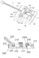
- FIG. 1 shows a schematic perspective view of a fixing apparatus according to an example embodiment of the disclosure.
- FIG. 2 shows a perspective view of a first fixing device 100 and a second fixing device 200 of the fixing apparatus shown in FIG. 1 .
- the fixing apparatus mainly comprises a first fixing device 100 adapted to position and fix a circuit board 1, and a second fixing device 200 adapted to position and fix at least one wire 2.
- FIG. 3 shows a schematic perspective view of the second fixing device 200 shown in FIG. 2 with a pressing cover 220 being in an open state
- FIG. 5 shows a schematic perspective view of the first fixing device 100 shown in FIG. 2 with a first locking device 130 being in a lock position.
- the first fixing device 100 is formed with a first positioning groove 111 adapted to position the circuit board 1 having at least one pad 1a.
- the second fixing device 200 is formed with at least one second positioning groove 211 adapted to position the at least one wire 2 to be electrically connected to the at least one pads of the circuit board 1, respectively.
- each second positioning groove 211 is aligned with a corresponding pad 1a on the circuit board 1 so that the wire 2 fixed in the second positioning groove 211 is aligned with the corresponding pad 1a on the circuit board 1.
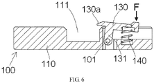
- FIG. 6 shows a cross-sectional view of the first fixing device 100 shown in FIG. 2 with a first lock 130 being in an unlocked position.
- the first fixing device 100 mainly comprises a first fixing base 110 and the first lock 130.
- the first positioning groove 111 is formed in the first fixing base 110 and extending in an axial direction of the wire 2.
- the first lock 130 is pivotally connected to a side of the first fixing base 110 and adapted to be rotated between a locked position and the unlocked position.
- the first lock 130 is adapted to hold and lock the circuit board 1 in the first positioning groove 111 when being in the locking position.
- the first lock 130 is formed with a first locking lip 130 extending from one end thereof (left end in Fig. 6 ) toward the first positioning groove 111 and adapted to be locked onto an edge portion of the circuit board 1. In this way, the circuit board 1 is held in the first positioning groove 111.
- the first lock 130 has a connection portion 131 pivotally connected to the first fixing base 110 between both ends thereof.
- the first fixing base 110 is provided with a first spring 140 extending in a thickness direction of the second fixing base 210 and adapted to push the other of the first lock 130 upwardly to hold the first lock 130 in the locked position.
- the first lock 130 when the first lock 130 is applied with a downward pressing force F at the other end thereof (right end in Fig. 6 ) against the first spring 140, the first lock 130 may overcome a thrust of the first spring 140 to be rotated from the locked position to the unlocked position, so that the first lock 130 is disengaged from the circuit board 1.
- the first lock 130 when the downward pressing force F applied to the other end of the first lock 130 is released, the first lock 130 may be automatically rotated from the unlock position to the locked position under the thrust of the first spring 140.
- the first fixing base 110 is formed with a receiving slot 112 extending in a direction perpendicular to the axial direction of the wire 2, in which the first lock 130 and the first spring 140 are disposed.
- the connection portion 131 of the first lock 130 is pivotally connected to a sidewall of the receiving slot 112 by a pivot shaft 101.
- FIG. 4 shows a cross-sectional view of the second fixing device 200 shown in FIG. 3 with the pressing cover 220 being in the open state.
- the second fixing device 200 mainly comprises a second fixing base 210, the pressing cover 220 and a second lock 230.
- the second positioning groove 211 is formed in the second fixing base 210.
- the pressing cover 220 is pivotally connected to a side of the second fixing base 210 and adapted to be rotated between the open state and the closed state.
- the second lock 230 is pivotally connected to the other side of the second fixing base 210 opposite to the one side and adapted to be rotated between a locked position and an unlocked position.
- the pressing cover 220 is adapted to press and hold the wire 2 in the second positioning groove 211 when being in the closed state.
- the second lock 230 is adapted to lock the pressing cover 220 in the closed state when being in the locked position.
- the second lock 230 is formed with a second locking lip 230a which extends from one end thereof (upper end in Fig. 4 ) toward the second positioning groove 211 and is adapted to be locked onto an edge portion of the pressing cover 220.
- the second lock 230 is pivotally connected to the second fixing base 210 at the other end thereof opposite to the one side (lower end in Fig. 4 ).
- the second fixing base 210 is provided with a second spring 240 extending in the direction perpendicular to the axial direction of the wire 2, one end of which is pressed against one end of the second lock 230 to hold the second lock 230 in the locked position.
- the second lock 230 when the second lock 230 is applied with a driving force against a thrust of the second spring 240 at the one end thereof, the second lock 230 may overcome the thrust of the spring 240 to be rotated from the locked position to the unlocked position so that the second lock 230 is disengaged from the pressing cover 220.
- the second lock 230 when the driving force applied to one end of the second lock 230 is released, the second lock 230 may be automatically rotated from the unlocked position to the locked position under the thrust of the second spring 240.
- the pressing cover 220 is pivotally connected to the second fixing base 210 at one end thereof by a first pivot shaft 201.
- the second lock 230 is pivotally connected to the second fixing base 210 at the other end thereof (lower end in Fig. 4 ) by a second pivot shaft 202.
- the second fixing base 210 is formed with a pressing tongue 213 horizontally forwardly extending toward the first fixing base 110 in the axial direction of the wire 2, and the second positioning groove 211 is formed on surfaces of the pressing tongue 213 and the second fixing base 210.
- the pressing tongue 213 is adapted to press an end portion 2a of the wire 2 fixed in the second positioning groove 211 against a corresponding pad 1a on the circuit board 1.
- the fixing apparatus further comprises a mounting base 10 onto which the first fixing device 100 and the second fixing device 200 are mounted.
- the second fixing base 210 is formed with a semicircular positioning recess 212 at either end thereof, respectively.
- the mounting base 10 is formed with two support platforms 11, each of which is formed with a circular positioning post 12.
- the second fixing base 210 are supported on the two support platforms 11 at both ends thereof, respectively, and the positioning posts 12 are fitted in the positioning recesses 212 of the second fixing base 210, respectively.
- the second fixing device 200 before connecting the wires 2 to the circuit board 1, the second fixing device 200 is firstly disassembled from the mounting base 10; the wires are clamped between the pressing cover 220 and the second fixing base 210; and the second fixing device 200 is then mounted onto the mounting base 10 by the positioning posts 12 and the positioning recesses 212. After the second fixing device 200 is mounted onto the mounting base 10, the pressing cover 220 is located below the second fixing base 210 and faces a surface of the mounting base 10.
- the pressing cover 220 is not in contact the surface of the mounting base 10, so that the second fixing device 200 is suspended and supported on the mounting base 10 by the two support platforms 11.
- the fixing apparatus may comprise a plurality of first fixing devices 100 arranged in a row to allow a plurality of circuit boards 1 to be simultaneously positioned and fixed.
- the fixing apparatus may comprise a plurality of second fixing devices 200 arranged in a row to allow a plurality of rows of wires 2 to be simultaneously positioned and fixed. In this way, it is possible to simultaneously solder the plurality of rows of wires 2 to the plurality of circuit boards 1 respectively, thereby improving the soldering efficiency.
Landscapes
- Engineering & Computer Science (AREA)
- Microelectronics & Electronic Packaging (AREA)
- Manufacturing & Machinery (AREA)
- Metallurgy (AREA)
- Mounting Of Printed Circuit Boards And The Like (AREA)
- Clamps And Clips (AREA)
- Insertion, Bundling And Securing Of Wires For Electric Apparatuses (AREA)
- Installation Of Indoor Wiring (AREA)
Abstract
Description
- This application claims the benefit of Chinese Patent Application No.
CN201710024577.X filed on January 13, 2017 - Embodiments of the disclosure relate to a fixing apparatus, and in particular to a fixing apparatus adapted to position and fix a circuit board and a wire.
- In the field of electronics manufacturing technique, a circuit board and a wire are often required to be accurately positioned and fixed. For example, in the prior art, it is often to solder an elongated wire to a pad of the circuit board. In order to ensure soldering accuracy, In order to ensure the soldering accuracy, the wire and the circuit board are needed to be accurately positioned and fixed at a predetermined position in advance so that the wire is accurately aligned with the corresponding pad on the circuit board.
- Currently, there is no such fixing device adapted to accurately position and fix the circuit board and the wire. Therefore, in the prior art, the circuit board and the wire are usually manually positioned and fixed, which undoubtedly reduces the soldering accuracy, thereby reducing the quality of a soldered product.
- Embodiments of the disclosure have been made to overcome or alleviate at least one aspect of the above mentioned disadvantages.
- At least one embodiment of the disclosure provides a fixing apparatus adapted to accurately position and reliably hold a circuit board and a wire.
- According to one aspect of the disclosure, there is provided a fixing apparatus, comprising: a first fixing device adapted to position and fix a circuit board having at least one pad; and a second fixing device adapted to position and fix at least one wire. The first fixing device is formed with a first positioning groove adapted to position the circuit board, and the second fixing device is formed with at least one second positioning groove adapted to position the at least one wire. The second positioning groove each is aligned with a corresponding pad on the circuit board so that the wire fixed in the second positioning groove is aligned with the corresponding pad on the circuit board.
- According to an exemplary embodiment of the disclosure, the first fixing device comprises: a first fixing base in which the first positioning groove is formed; and a first lock pivotally connected to a side of the first fixing base and adapted to be rotated between a locked position and the unlocked position. The first lock is adapted to hold and lock the circuit board in the first positioning groove when being in the locking position.
- According to another exemplary embodiment of the disclosure, the first lock is formed with a first locking lip extending from one end thereof and adapted to lock an edge portion of the circuit board.
- According to further another exemplary embodiment of the disclosure, the first lock has a connection portion pivotally connected to the first fixing base between both ends thereof.
- According to yet another exemplary embodiment of the disclosure, the first fixing base is provided with a first spring adapted to push the other of the first lock upwardly to hold the first lock in the locked position.
- According to still another exemplary embodiment of the disclosure, when the first lock is applied with a downward pressing force at the other end thereof, the first lock overcomes a thrust of the first spring to be rotated from the locked position to the unlocked position, so that the first lock is separated from the circuit board.
- According to further another exemplary embodiment of the disclosure, the first fixing base is formed with a receiving slot in which the first lock and the first spring are disposed. The connection portion of the first lock is pivotally connected to a sidewall of the receiving slot by a pivot shaft.
- According to yet another exemplary embodiment of the disclosure, the second fixing device comprises: a second fixing base in which the second positioning groove is formed; a pressing cover pivotally connected to a side of the second fixing base and adapted to be rotated between an open state and an closed state; and a second lock pivotally connected to the other side of the second fixing base and adapted to be rotated between a locked position and an unlocked position. The pressing cover is adapted to press the wire in the second positioning groove when being in the closed state, and the second lock is adapted to lock the pressing cover in the closed state when being in the locked position.
- According to still another exemplary embodiment of the disclosure, the second lock is formed with a second locking lip extending from one end thereof toward the second positioning groove and adapted to lock an edge portion of the pressing cover.
- According to further another exemplary embodiment of the disclosure, the second lock is pivotally connected to the second fixing base at the other end thereof.
- According to yet another exemplary embodiment of the disclosure, the second fixing base is provided with a second spring, one end of which is pressed against one end of the second lock to hold the second lock in the locked position.
- According to still another exemplary embodiment of the disclosure, when the second lock is applied with a driving force against a thrust of the second spring at one end thereof, the second lock overcomes the thrust of the spring to be rotated from the locked position to the unlocked position so that the second lock is disengaged from the pressing cover.
- According to further another exemplary embodiment of the disclosure, the pressing cover is pivotally connected to the second fixing base at one end thereof by a first pivot shaft. The second lock is pivotally connected to the second fixing base at the other end thereof by a second pivot shaft.
- According to yet another exemplary embodiment of the disclosure, the second fixing base is formed with a pressing tongue horizontally forwardly extending, and the second positioning groove is formed on surfaces of the pressing tongue and the second fixing base. The pressing tongue is adapted to press an end portion of the wire fixed in the second positioning groove against a corresponding pad on the circuit board.
- According to still another exemplary embodiment of the disclosure, the fixing apparatus further comprises a mounting base onto which the first fixing device and the second fixing device are mounted.
- According to further another exemplary embodiment of the disclosure, the second fixing base is formed with a semicircular positioning recess at either end thereof, respectively. The mounting base is formed with two support platforms, each of which is formed with a circular positioning post. The second fixing base is supported on the two support platforms at both ends thereof, respectively, and the positioning posts are fitted in the positioning recesses of the second fixing base, respectively.
- According to yet another exemplary embodiment of the disclosure, after the second fixing device is mounted onto the mounting base, the pressing cover is located below the second fixing base and faces a surface of the mounting base.
- According to still another exemplary embodiment of the disclosure, after the second fixing device is mounted onto the mounting base, the pressing cover is not in contact the surface of the mounting base, so that the second fixing device is suspended and supported on the mounting base by the two support platforms.
- According to further another exemplary embodiment of the disclosure, the fixing apparatus further comprises: a plurality of first fixing devices arranged in a row to allow a plurality of circuit boards to be simultaneously positioned and fixed; and a plurality of second fixing devices arranged in a row to allow a plurality of rows of wires to be simultaneously positioned and fixed.
- In the above-described various embodiments of the disclosure, the circuit board and the wire may be accurately positioned and reliably held in the corresponding positioning grooves, thereby improving the positioning accuracy and reliability of the wire and the circuit board, which facilitates to improving the accuracy of soldering the wire to the circuit board.
- Other objects and advantages of the disclosure will become apparent from the following description of the disclosure when taken in conjunction with the accompanying drawings, and may give a comprehensive understanding of the disclosure.
- The above and other features of the disclosure will become more apparent by describing in detail exemplary embodiments thereof with reference to the accompanying drawings, in which:
-
FIG. 1 shows a schematic perspective view of a fixing apparatus according to an example embodiment of the disclosure; -
FIG. 2 shows a schematic perspective view of a first fixing device and a second fixing device of the fixing apparatus shown inFIG. 1 ; -
FIG. 3 shows a schematic perspective view of the second fixing device shown inFIG. 2 with a pressing cover being in an open state; -
FIG. 4 shows a cross-sectional view of the second fixing device shown inFIG. 3 with the pressing being in the open state; -
FIG. 5 shows a schematic perspective view of the first fixing device shown inFIG. 2 with a first lock being in a locking position; and -
FIG. 6 shows a cross-sectional view of the first fixing device shown inFIG. 2 with the first lock being in an unlocked position. - The technical solution of the disclosure will be described hereinafter in further detail with reference to the following embodiments, taken in conjunction with the accompanying drawings. In the specification, the same or similar reference numerals indicate the same or similar parts. The description of the embodiments of the disclosure hereinafter with reference to the accompanying drawings is intended to explain the general inventive concept of the disclosure and should not be construed as a limitation on the disclosure.
- In addition, in the following detailed description, for the sake of explanation, numerous specific details are set forth in order to provide a thorough understanding of the disclosed embodiments. It will be apparent, however, that one or more embodiments may also be practiced without these specific details. In other instances, well-known structures and devices are illustrated schematically in order to simplify the drawing.
- According to a general technical concept of the disclosure, there is provided a fixing apparatus, comprising: a first fixing device adapted to position and fix a circuit board having at least one pad; and a second fixing device adapted to position and fix at least one wire. The first fixing device is formed with a first positioning groove adapted to position the circuit board, and the second fixing device is formed with at least one second positioning groove adapted to position the at least one wire. Each second positioning groove is aligned with a corresponding pad on the circuit board so that the wire fixed in the second positioning groove is aligned with the corresponding pad on the circuit board.
-
FIG. 1 shows a schematic perspective view of a fixing apparatus according to an example embodiment of the disclosure.FIG. 2 shows a perspective view of afirst fixing device 100 and asecond fixing device 200 of the fixing apparatus shown inFIG. 1 . - As shown in
FIGS. 1 and2 , in the illustrated embodiment, the fixing apparatus mainly comprises afirst fixing device 100 adapted to position and fix acircuit board 1, and asecond fixing device 200 adapted to position and fix at least onewire 2. -
FIG. 3 shows a schematic perspective view of thesecond fixing device 200 shown inFIG. 2 with apressing cover 220 being in an open state;FIG. 5 shows a schematic perspective view of thefirst fixing device 100 shown inFIG. 2 with afirst locking device 130 being in a lock position. - As shown in
FIG. 5 , in the illustrated embodiment, thefirst fixing device 100 is formed with afirst positioning groove 111 adapted to position thecircuit board 1 having at least onepad 1a. As shown inFIG. 3 , in the illustrated embodiment, thesecond fixing device 200 is formed with at least onesecond positioning groove 211 adapted to position the at least onewire 2 to be electrically connected to the at least one pads of thecircuit board 1, respectively. - As shown in
FIGS. 2, 3 and5 , in the illustrated embodiment, eachsecond positioning groove 211 is aligned with acorresponding pad 1a on thecircuit board 1 so that thewire 2 fixed in thesecond positioning groove 211 is aligned with thecorresponding pad 1a on thecircuit board 1. -
FIG. 6 shows a cross-sectional view of thefirst fixing device 100 shown inFIG. 2 with afirst lock 130 being in an unlocked position. - As shown in
FIGS. 5 and6 , in the illustrated embodiment, thefirst fixing device 100 mainly comprises afirst fixing base 110 and thefirst lock 130. Thefirst positioning groove 111 is formed in thefirst fixing base 110 and extending in an axial direction of thewire 2. Thefirst lock 130 is pivotally connected to a side of thefirst fixing base 110 and adapted to be rotated between a locked position and the unlocked position. - As shown in
FIG. 5 , in the illustrated embodiment, thefirst lock 130 is adapted to hold and lock thecircuit board 1 in thefirst positioning groove 111 when being in the locking position. - As shown in
FIGS. 5 and6 , in the illustrated embodiment, thefirst lock 130 is formed with afirst locking lip 130 extending from one end thereof (left end inFig. 6 ) toward thefirst positioning groove 111 and adapted to be locked onto an edge portion of thecircuit board 1. In this way, thecircuit board 1 is held in thefirst positioning groove 111. - As shown in
FIGS. 5 and6 , in the illustrated embodiment, thefirst lock 130 has aconnection portion 131 pivotally connected to thefirst fixing base 110 between both ends thereof. - As shown in
FIG. 5 andFIG. 6 , in the illustrated embodiment, thefirst fixing base 110 is provided with afirst spring 140 extending in a thickness direction of thesecond fixing base 210 and adapted to push the other of thefirst lock 130 upwardly to hold thefirst lock 130 in the locked position. - As shown in
FIGS. 5 and6 , in the illustrated embodiment, when thefirst lock 130 is applied with a downward pressing force F at the other end thereof (right end inFig. 6 ) against thefirst spring 140, thefirst lock 130 may overcome a thrust of thefirst spring 140 to be rotated from the locked position to the unlocked position, so that thefirst lock 130 is disengaged from thecircuit board 1. - As shown in
FIGS. 5 and6 , in the illustrated embodiment, when the downward pressing force F applied to the other end of thefirst lock 130 is released, thefirst lock 130 may be automatically rotated from the unlock position to the locked position under the thrust of thefirst spring 140. - As shown in
FIGS. 5 and6 , in the illustrated embodiment, thefirst fixing base 110 is formed with a receivingslot 112 extending in a direction perpendicular to the axial direction of thewire 2, in which thefirst lock 130 and thefirst spring 140 are disposed. Theconnection portion 131 of thefirst lock 130 is pivotally connected to a sidewall of the receivingslot 112 by apivot shaft 101. -
FIG. 4 shows a cross-sectional view of thesecond fixing device 200 shown inFIG. 3 with thepressing cover 220 being in the open state. - As shown in
FIGS. 3 and4 , in the illustrated embodiment, thesecond fixing device 200 mainly comprises asecond fixing base 210, thepressing cover 220 and asecond lock 230. Thesecond positioning groove 211 is formed in thesecond fixing base 210. Thepressing cover 220 is pivotally connected to a side of thesecond fixing base 210 and adapted to be rotated between the open state and the closed state. Thesecond lock 230 is pivotally connected to the other side of thesecond fixing base 210 opposite to the one side and adapted to be rotated between a locked position and an unlocked position. - As shown in
FIG.S 2 and 3pressing cover 220 is adapted to press and hold thewire 2 in thesecond positioning groove 211 when being in the closed state. Thesecond lock 230 is adapted to lock thepressing cover 220 in the closed state when being in the locked position. - As shown in
FIGS. 3 and4 , in the illustrated embodiment, thesecond lock 230 is formed with asecond locking lip 230a which extends from one end thereof (upper end inFig. 4 ) toward thesecond positioning groove 211 and is adapted to be locked onto an edge portion of thepressing cover 220. - As shown in
FIGS. 3 and4 , in the illustrated embodiment, thesecond lock 230 is pivotally connected to thesecond fixing base 210 at the other end thereof opposite to the one side (lower end inFig. 4 ). - As shown in
FIGS. 3 and4 , in the illustrated embodiment, thesecond fixing base 210 is provided with asecond spring 240 extending in the direction perpendicular to the axial direction of thewire 2, one end of which is pressed against one end of thesecond lock 230 to hold thesecond lock 230 in the locked position. - As shown in
FIGS. 3 and4 , in the illustrated embodiment, when thesecond lock 230 is applied with a driving force against a thrust of thesecond spring 240 at the one end thereof, thesecond lock 230 may overcome the thrust of thespring 240 to be rotated from the locked position to the unlocked position so that thesecond lock 230 is disengaged from thepressing cover 220. - As shown in
FIGS. 3 and4 , in the illustrated embodiment, when the driving force applied to one end of thesecond lock 230 is released, thesecond lock 230 may be automatically rotated from the unlocked position to the locked position under the thrust of thesecond spring 240. - As shown in
FIGS. 3 and4 , in the illustrated embodiment, thepressing cover 220 is pivotally connected to thesecond fixing base 210 at one end thereof by afirst pivot shaft 201. Further, thesecond lock 230 is pivotally connected to thesecond fixing base 210 at the other end thereof (lower end inFig. 4 ) by asecond pivot shaft 202. - As shown in
FIGS. 2 and FIG. 3 , in the illustrated embodiment, thesecond fixing base 210 is formed with apressing tongue 213 horizontally forwardly extending toward thefirst fixing base 110 in the axial direction of thewire 2, and thesecond positioning groove 211 is formed on surfaces of thepressing tongue 213 and thesecond fixing base 210. As shown inFIG. 2 , thepressing tongue 213 is adapted to press anend portion 2a of thewire 2 fixed in thesecond positioning groove 211 against acorresponding pad 1a on thecircuit board 1. - As shown in
FIGS. 1 and2 , in the illustrated embodiment, the fixing apparatus further comprises a mountingbase 10 onto which thefirst fixing device 100 and thesecond fixing device 200 are mounted. - As shown in
FIGS. 2 and 3 , in the illustrated embodiment, thesecond fixing base 210 is formed with asemicircular positioning recess 212 at either end thereof, respectively. The mountingbase 10 is formed with twosupport platforms 11, each of which is formed with acircular positioning post 12. Thesecond fixing base 210 are supported on the twosupport platforms 11 at both ends thereof, respectively, and the positioning posts 12 are fitted in the positioning recesses 212 of thesecond fixing base 210, respectively. - As shown in
FIGS. 1-3 , in the illustrated embodiment, before connecting thewires 2 to thecircuit board 1, thesecond fixing device 200 is firstly disassembled from the mountingbase 10; the wires are clamped between thepressing cover 220 and thesecond fixing base 210; and thesecond fixing device 200 is then mounted onto the mountingbase 10 by the positioning posts 12 and the positioning recesses 212. After thesecond fixing device 200 is mounted onto the mountingbase 10, thepressing cover 220 is located below thesecond fixing base 210 and faces a surface of the mountingbase 10. - As shown in
FIGS. 2 and 3 , in the illustrated embodiment, after thesecond fixing device 200 is mounted onto the mountingbase 10, thepressing cover 220 is not in contact the surface of the mountingbase 10, so that thesecond fixing device 200 is suspended and supported on the mountingbase 10 by the twosupport platforms 11. - As shown in
FIG. 1 , in the illustrated embodiment, the fixing apparatus may comprise a plurality offirst fixing devices 100 arranged in a row to allow a plurality ofcircuit boards 1 to be simultaneously positioned and fixed. The fixing apparatus may comprise a plurality ofsecond fixing devices 200 arranged in a row to allow a plurality of rows ofwires 2 to be simultaneously positioned and fixed. In this way, it is possible to simultaneously solder the plurality of rows ofwires 2 to the plurality ofcircuit boards 1 respectively, thereby improving the soldering efficiency. - It should be appreciated by those skilled in this art that the above embodiments are intended to be illustrative, and many modifications may be made to the above embodiments by those skilled in this art, and various structures described in various embodiments may be freely combined with each other without conflicting in configuration or principle.
- Although the disclosure have been described hereinbefore in detail with reference to the attached drawings, it should be appreciated that the disclosed embodiments in the attached drawings are intended to illustrate the preferred embodiments of the disclosure by way of example, and should not be construed as limitation to the disclosure.
- Although several exemplary embodiments have been shown and described, it would be appreciated by those skilled in the art that various changes or modifications may be made to these embodiments without departing from the principles and spirit of the disclosure, the scope of which is defined by the claims and their equivalents.
- It should be noted that, the word "comprise" doesn't exclude other elements or steps, and the word "a" or "an" doesn't exclude more than one. In addition, any reference numerals in the claims should not be interpreted as the limitation to the scope of the disclosure.
Claims (15)
- A fixing apparatus, comprising:a first fixing device (100) adapted to position and fix a circuit board (1) having at least one pad (1a); anda second fixing device (200) adapted to position and fix at least one wire (2),characterized in thatthe first fixing device (100) is formed with a first positioning groove (111) adapted to position the circuit board (1), and the second fixing device (200) is formed with at least one second positioning groove (211) adapted to position the at least one wire (2); andeach second positioning groove (211) is aligned with a corresponding pad (1a) on the circuit board (1) so that the wire (2) fixed in the second positioning groove (211) is aligned with the corresponding pad (1a) on the circuit board (1).
- The fixing apparatus according to claim 1, characterized in that
the first fixing device (100) comprises:a first fixing base (110) in which the first positioning groove (111) is formed; anda first lock (130) pivotally connected to a side of the first fixing base (110) and adapted to be rotated between a locked position and the unlocked position,wherein the first lock (130) is adapted to hold and lock the circuit board (1) in the first positioning groove (111) when being in the locking position. - The fixing apparatus according to claim 2, characterized in that the first lock (130) is formed with a first locking lip (130) extending from one end thereof and adapted to lock an edge portion of the circuit board (1).
- The fixing apparatus according to claim 2 or 3, characterized in that the first lock (130) has a connection portion (131) pivotally connected to the first fixing base (110) between both ends thereof.
- The fixing apparatus according to any one of claims 2 to 4, characterized in that
the first fixing base (110) is provided with a first spring (140) adapted to push the other of the first lock (130) upwardly to hold the first lock (130) in the locked position; and
when the first lock (130) is applied with a downward pressing force at the other end thereof, the first lock (130) overcomes a thrust of the first spring (140) to be rotated from the locked position to the unlocked position, so that the first lock (130) is separated from the circuit board (1). - The fixing apparatus according to claim 5, characterized in that
the first fixing base (110) is formed with a receiving slot (112) in which the first lock (130) and the first spring (140) are disposed; and
the connection portion (131) of the first lock (130) is pivotally connected to a sidewall of the receiving slot (112) by a pivot shaft (101). - The fixing apparatus according to any one of claims 1 to 6, characterized in that
the second fixing device (200) comprises:a second fixing base (210) in which the second positioning groove (211) is formed;a pressing cover (220) pivotally connected to a side of the second fixing base (210) and adapted to be rotated between an open state and an closed state; anda second lock (230) pivotally connected to the other side of the second fixing base (210) and adapted to be rotated between a locked position and an unlocked position,wherein the pressing cover (220) is adapted to press the wire (2) in the second positioning groove (211) when being in the closed state; and the second lock (230) is adapted to lock the pressing cover (220) in the closed state when being in the locked position. - The fixing apparatus according to claim 7, characterized in that
the second lock (230) is formed with a second locking lip (230a) extending from one end thereof toward the second positioning groove and adapted to locked an edge portion of the pressing cover (220); and
the second lock (230) is pivotally connected to the second fixing base (210) at the other end thereof. - The fixing apparatus according to claim 7 or 8, characterized in that
the second fixing base (210) is provided with a second spring (240), one end of which is pressed against one end of the second lock (230) to hold the second lock (230) in the locked position; and
when the second lock (230) is applied with a driving force against a thrust of the second spring (240) at one end thereof, the second lock (230) overcomes the thrust of the spring (240) to be rotated from the locked position to the unlocked position so that the second lock (230) is disengaged from the pressing cover (220). - The fixing apparatus according to any one of claims 7 to 9, characterized in that
the pressing cover (220) is pivotally connected to the second fixing base (210) at one end thereof by a first pivot shaft (201); and
the second lock (230) is pivotally connected to the second fixing base (210) at the other end thereof by a second pivot shaft (202). - The fixing apparatus according to any one of claims 7 to 10, characterized in that
the second fixing base (210) is formed with a pressing tongue (213) horizontally forwardly extending, and the second positioning groove (211) is formed on surfaces of the pressing tongue (213) and the second fixing base (210); and
the pressing tongue (213) is adapted to press an end portion (2a) of the wire (2) fixed in the second positioning groove (211) against a corresponding pad (1a) on the circuit board (1). - The fixing apparatus according to any one of claims 7 to 11, characterized in that further comprising a mounting base (10) onto which the first fixing device (100) and the second fixing device (200) are mounted;
wherein the second fixing base (210) is formed with a semicircular positioning recess (212) at either end thereof, respectively; and the mounting base (10) is formed with two support platforms (11), each of which is formed with a circular positioning post (12); and
wherein the second fixing base (210) are supported on the two support platforms (11) at both ends thereof, respectively, and the positioning posts (12) are fitted in the positioning recesses (212) of the second fixing base (210), respectively. - The fixing apparatus according to claim 12, characterized in that after the second fixing device (200) is mounted onto the mounting base (10), the pressing cover (220) is located below the second fixing base (210) and faces a surface of the mounting base (10).
- The fixing apparatus according to claim 12 or 13, characterized in that after the second fixing device (200) is mounted onto the mounting base (10), the pressing cover (220) is not in contact the surface of the mounting base (10), so that the second fixing device (200) is suspended and supported on the mounting base (10) by the two support platforms (11).
- The fixing apparatus according to any one of claims 1 to 14, characterized in that further comprising:a plurality of first fixing devices (100) arranged in a row to allow a plurality of circuit boards (1) to be simultaneously positioned and fixed; anda plurality of second fixing devices (200) arranged in a row to allow a plurality of rows of wires (2) to be simultaneously positioned and fixed.
Applications Claiming Priority (1)
| Application Number | Priority Date | Filing Date | Title |
|---|---|---|---|
| CN201710024577.XA CN108307586B (en) | 2017-01-13 | 2017-01-13 | Fixing device |
Publications (2)
| Publication Number | Publication Date |
|---|---|
| EP3349550A1 true EP3349550A1 (en) | 2018-07-18 |
| EP3349550B1 EP3349550B1 (en) | 2024-04-24 |
Family
ID=61017771
Family Applications (1)
| Application Number | Title | Priority Date | Filing Date |
|---|---|---|---|
| EP18151590.9A Active EP3349550B1 (en) | 2017-01-13 | 2018-01-15 | Fixing apparatus |
Country Status (3)
| Country | Link |
|---|---|
| US (1) | US11160173B2 (en) |
| EP (1) | EP3349550B1 (en) |
| CN (1) | CN108307586B (en) |
Cited By (2)
| Publication number | Priority date | Publication date | Assignee | Title |
|---|---|---|---|---|
| CN110977300A (en) * | 2019-12-24 | 2020-04-10 | 深圳市利宏微形电机有限公司 | Plate and wire welding clamp |
| CN116487967A (en) * | 2023-06-07 | 2023-07-25 | 中山市联纵智能科技有限公司 | A magazine, a welding mold and a welding method |
Families Citing this family (7)
| Publication number | Priority date | Publication date | Assignee | Title |
|---|---|---|---|---|
| CN109079388B (en) * | 2017-06-14 | 2020-06-19 | 泰科电子(上海)有限公司 | Fixing device for welding and welding method |
| USD852764S1 (en) * | 2017-12-21 | 2019-07-02 | David W. Cline | Circuit breaker board for a portable isolation power supply |
| USD906272S1 (en) * | 2018-12-31 | 2020-12-29 | David W. Cline | Circuit breaker board for a portable isolation power supply |
| USD904324S1 (en) * | 2018-12-31 | 2020-12-08 | David W. Cline | Circuit breaker board for a portable isolation power supply |
| CN114040597A (en) * | 2021-12-06 | 2022-02-11 | 珠海富元电子科技有限公司 | Combined large display board |
| CN116600494A (en) * | 2022-02-07 | 2023-08-15 | 泰科电子(上海)有限公司 | Fixtures, alignment systems and alignment methods |
| CN118438099A (en) * | 2024-06-03 | 2024-08-06 | 龙旗电子(惠州)有限公司 | Battery welding jig |
Citations (5)
| Publication number | Priority date | Publication date | Assignee | Title |
|---|---|---|---|---|
| JPS566462A (en) * | 1979-06-27 | 1981-01-23 | Mitsubishi Electric Corp | Positioning method |
| JPS63287047A (en) * | 1987-05-19 | 1988-11-24 | Sanyo Electric Co Ltd | Method for fixing outer-lead of hybrid integrated circuit |
| JPH11104820A (en) * | 1997-09-30 | 1999-04-20 | Pentel Kk | Positioning jig for soldering |
| US20130186941A1 (en) * | 2012-01-24 | 2013-07-25 | Apple Inc. | Induction bonding |
| US20140191457A1 (en) * | 2010-12-03 | 2014-07-10 | Volex Plc | Wire holder and method of terminating wire conductors |
Family Cites Families (7)
| Publication number | Priority date | Publication date | Assignee | Title |
|---|---|---|---|---|
| US3972463A (en) * | 1975-02-07 | 1976-08-03 | Rca Corporation | Wire placement fixture |
| US8512066B2 (en) * | 2009-09-17 | 2013-08-20 | Jowoo-Tech Co. Ltd | Electric wire connector for press connecting electric wires |
| CN202353953U (en) * | 2011-10-29 | 2012-07-25 | 昆山明创电子科技有限公司 | Solder pallet fixture |
| CN103178427A (en) * | 2011-12-21 | 2013-06-26 | 苏州精实电子科技有限公司 | Jig for manufacturing signal transmission lines through welding and manufacturing process thereof |
| CN103401104A (en) * | 2013-08-13 | 2013-11-20 | 乐清市八达光电科技有限公司 | Alternating current charging socket with power-off upon cover opening function |
| CN204560047U8 (en) * | 2015-02-16 | 2016-07-27 | 惠州市顺源科技有限公司 | A kind of Wave soldering fixture |
| CN204741621U (en) * | 2015-06-01 | 2015-11-04 | 江苏云意电气股份有限公司 | Automobile power generation machine regulator IC and disposable welded structure of PCB board |
-
2017
- 2017-01-13 CN CN201710024577.XA patent/CN108307586B/en active Active
-
2018
- 2018-01-11 US US15/867,911 patent/US11160173B2/en active Active
- 2018-01-15 EP EP18151590.9A patent/EP3349550B1/en active Active
Patent Citations (5)
| Publication number | Priority date | Publication date | Assignee | Title |
|---|---|---|---|---|
| JPS566462A (en) * | 1979-06-27 | 1981-01-23 | Mitsubishi Electric Corp | Positioning method |
| JPS63287047A (en) * | 1987-05-19 | 1988-11-24 | Sanyo Electric Co Ltd | Method for fixing outer-lead of hybrid integrated circuit |
| JPH11104820A (en) * | 1997-09-30 | 1999-04-20 | Pentel Kk | Positioning jig for soldering |
| US20140191457A1 (en) * | 2010-12-03 | 2014-07-10 | Volex Plc | Wire holder and method of terminating wire conductors |
| US20130186941A1 (en) * | 2012-01-24 | 2013-07-25 | Apple Inc. | Induction bonding |
Cited By (3)
| Publication number | Priority date | Publication date | Assignee | Title |
|---|---|---|---|---|
| CN110977300A (en) * | 2019-12-24 | 2020-04-10 | 深圳市利宏微形电机有限公司 | Plate and wire welding clamp |
| CN110977300B (en) * | 2019-12-24 | 2021-04-13 | 深圳市利宏微形电机有限公司 | Plate and wire welding clamp |
| CN116487967A (en) * | 2023-06-07 | 2023-07-25 | 中山市联纵智能科技有限公司 | A magazine, a welding mold and a welding method |
Also Published As
| Publication number | Publication date |
|---|---|
| CN108307586B (en) | 2020-08-28 |
| US11160173B2 (en) | 2021-10-26 |
| US20180206344A1 (en) | 2018-07-19 |
| EP3349550B1 (en) | 2024-04-24 |
| CN108307586A (en) | 2018-07-20 |
Similar Documents
| Publication | Publication Date | Title |
|---|---|---|
| EP3349550B1 (en) | Fixing apparatus | |
| US20190229445A1 (en) | Conductive Terminal And Connector Assembly | |
| CN114069285B (en) | Connector assembly | |
| KR102316920B1 (en) | Printed circuit board with side access termination pads | |
| KR20130113499A (en) | Board connecting terminal and holding structure of circuit board | |
| US20180190561A1 (en) | Easily detachable cpu clip | |
| EP2884827A2 (en) | Socket | |
| US9106006B2 (en) | Connector having an anisotropic conductive film | |
| US7534133B2 (en) | Electrical connector assembly with alignment pin | |
| US5730630A (en) | Apparatus for mounting connector to circuit board | |
| EP3351346B1 (en) | Fixing device | |
| US5885097A (en) | Electrical connector with a board locking device | |
| US10629870B1 (en) | Circuit board and battery holder thereof | |
| KR970002790Y1 (en) | Pin holding device | |
| US5911584A (en) | Circuit card connector with isolation base assembly | |
| US6354856B1 (en) | IC socket and contact pin thereof | |
| CN101304128A (en) | Electrical connection terminal for connection hole and locking structure of electronic component provided with the terminal | |
| CN116298429A (en) | Electrical test contact terminal for plug-in device pins | |
| US20180076544A1 (en) | Socket with remoable retainer attached to deflectable fixing seat | |
| US4536055A (en) | Stamped and formed stacking device for circuit boards and a method for making | |
| JP4384316B2 (en) | Electronic component module | |
| EP3349312A1 (en) | Fixing apparatus | |
| US6993834B2 (en) | Apparatus for assembling card edge slots into a substrate | |
| JP2532427B2 (en) | Lead bending method and apparatus for electronic parts | |
| TW200403900A (en) | Contact for pin grid array connector and method of forming same |
Legal Events
| Date | Code | Title | Description |
|---|---|---|---|
| PUAI | Public reference made under article 153(3) epc to a published international application that has entered the european phase |
Free format text: ORIGINAL CODE: 0009012 |
|
| STAA | Information on the status of an ep patent application or granted ep patent |
Free format text: STATUS: THE APPLICATION HAS BEEN PUBLISHED |
|
| AK | Designated contracting states |
Kind code of ref document: A1 Designated state(s): AL AT BE BG CH CY CZ DE DK EE ES FI FR GB GR HR HU IE IS IT LI LT LU LV MC MK MT NL NO PL PT RO RS SE SI SK SM TR |
|
| AX | Request for extension of the european patent |
Extension state: BA ME |
|
| STAA | Information on the status of an ep patent application or granted ep patent |
Free format text: STATUS: REQUEST FOR EXAMINATION WAS MADE |
|
| 17P | Request for examination filed |
Effective date: 20190109 |
|
| RBV | Designated contracting states (corrected) |
Designated state(s): AL AT BE BG CH CY CZ DE DK EE ES FI FR GB GR HR HU IE IS IT LI LT LU LV MC MK MT NL NO PL PT RO RS SE SI SK SM TR |
|
| STAA | Information on the status of an ep patent application or granted ep patent |
Free format text: STATUS: EXAMINATION IS IN PROGRESS |
|
| 17Q | First examination report despatched |
Effective date: 20210622 |
|
| RAP1 | Party data changed (applicant data changed or rights of an application transferred) |
Owner name: TE CONNECTIVITY SOLUTIONS GMBH Owner name: MEASUREMENT SPECIALTIES (CHENGDU) LTD Owner name: TYCO ELECTRONICS (SHANGHAI) CO. LTD. |
|
| GRAP | Despatch of communication of intention to grant a patent |
Free format text: ORIGINAL CODE: EPIDOSNIGR1 |
|
| STAA | Information on the status of an ep patent application or granted ep patent |
Free format text: STATUS: GRANT OF PATENT IS INTENDED |
|
| INTG | Intention to grant announced |
Effective date: 20240105 |
|
| RAP3 | Party data changed (applicant data changed or rights of an application transferred) |
Owner name: TE CONNECTIVITY SOLUTIONS GMBH Owner name: MEASUREMENT SPECIALITIES (CHENGDU) LTD. Owner name: TYCO ELECTRONICS (SHANGHAI) CO., LTD. |
|
| GRAS | Grant fee paid |
Free format text: ORIGINAL CODE: EPIDOSNIGR3 |
|
| GRAA | (expected) grant |
Free format text: ORIGINAL CODE: 0009210 |
|
| STAA | Information on the status of an ep patent application or granted ep patent |
Free format text: STATUS: THE PATENT HAS BEEN GRANTED |
|
| AK | Designated contracting states |
Kind code of ref document: B1 Designated state(s): AL AT BE BG CH CY CZ DE DK EE ES FI FR GB GR HR HU IE IS IT LI LT LU LV MC MK MT NL NO PL PT RO RS SE SI SK SM TR |
|
| REG | Reference to a national code |
Ref country code: GB Ref legal event code: FG4D |
|
| REG | Reference to a national code |
Ref country code: CH Ref legal event code: EP |
|
| REG | Reference to a national code |
Ref country code: DE Ref legal event code: R096 Ref document number: 602018068437 Country of ref document: DE |
|
| REG | Reference to a national code |
Ref country code: IE Ref legal event code: FG4D |
|
| REG | Reference to a national code |
Ref country code: LT Ref legal event code: MG9D |
|
| REG | Reference to a national code |
Ref country code: NL Ref legal event code: MP Effective date: 20240424 |
|
| REG | Reference to a national code |
Ref country code: AT Ref legal event code: MK05 Ref document number: 1680991 Country of ref document: AT Kind code of ref document: T Effective date: 20240424 |
|
| PG25 | Lapsed in a contracting state [announced via postgrant information from national office to epo] |
Ref country code: NL Free format text: LAPSE BECAUSE OF FAILURE TO SUBMIT A TRANSLATION OF THE DESCRIPTION OR TO PAY THE FEE WITHIN THE PRESCRIBED TIME-LIMIT Effective date: 20240424 |
|
| PG25 | Lapsed in a contracting state [announced via postgrant information from national office to epo] |
Ref country code: NL Free format text: LAPSE BECAUSE OF FAILURE TO SUBMIT A TRANSLATION OF THE DESCRIPTION OR TO PAY THE FEE WITHIN THE PRESCRIBED TIME-LIMIT Effective date: 20240424 |
|
| PG25 | Lapsed in a contracting state [announced via postgrant information from national office to epo] |
Ref country code: IS Free format text: LAPSE BECAUSE OF FAILURE TO SUBMIT A TRANSLATION OF THE DESCRIPTION OR TO PAY THE FEE WITHIN THE PRESCRIBED TIME-LIMIT Effective date: 20240824 |
|
| PG25 | Lapsed in a contracting state [announced via postgrant information from national office to epo] |
Ref country code: BG Free format text: LAPSE BECAUSE OF FAILURE TO SUBMIT A TRANSLATION OF THE DESCRIPTION OR TO PAY THE FEE WITHIN THE PRESCRIBED TIME-LIMIT Effective date: 20240424 |
|
| PG25 | Lapsed in a contracting state [announced via postgrant information from national office to epo] |
Ref country code: HR Free format text: LAPSE BECAUSE OF FAILURE TO SUBMIT A TRANSLATION OF THE DESCRIPTION OR TO PAY THE FEE WITHIN THE PRESCRIBED TIME-LIMIT Effective date: 20240424 Ref country code: FI Free format text: LAPSE BECAUSE OF FAILURE TO SUBMIT A TRANSLATION OF THE DESCRIPTION OR TO PAY THE FEE WITHIN THE PRESCRIBED TIME-LIMIT Effective date: 20240424 |
|
| PG25 | Lapsed in a contracting state [announced via postgrant information from national office to epo] |
Ref country code: GR Free format text: LAPSE BECAUSE OF FAILURE TO SUBMIT A TRANSLATION OF THE DESCRIPTION OR TO PAY THE FEE WITHIN THE PRESCRIBED TIME-LIMIT Effective date: 20240725 |
|
| PG25 | Lapsed in a contracting state [announced via postgrant information from national office to epo] |
Ref country code: PT Free format text: LAPSE BECAUSE OF FAILURE TO SUBMIT A TRANSLATION OF THE DESCRIPTION OR TO PAY THE FEE WITHIN THE PRESCRIBED TIME-LIMIT Effective date: 20240826 |
|
| PG25 | Lapsed in a contracting state [announced via postgrant information from national office to epo] |
Ref country code: ES Free format text: LAPSE BECAUSE OF FAILURE TO SUBMIT A TRANSLATION OF THE DESCRIPTION OR TO PAY THE FEE WITHIN THE PRESCRIBED TIME-LIMIT Effective date: 20240424 |
|
| PG25 | Lapsed in a contracting state [announced via postgrant information from national office to epo] |
Ref country code: AT Free format text: LAPSE BECAUSE OF FAILURE TO SUBMIT A TRANSLATION OF THE DESCRIPTION OR TO PAY THE FEE WITHIN THE PRESCRIBED TIME-LIMIT Effective date: 20240424 |
|
| PG25 | Lapsed in a contracting state [announced via postgrant information from national office to epo] |
Ref country code: PL Free format text: LAPSE BECAUSE OF FAILURE TO SUBMIT A TRANSLATION OF THE DESCRIPTION OR TO PAY THE FEE WITHIN THE PRESCRIBED TIME-LIMIT Effective date: 20240424 |
|
| PG25 | Lapsed in a contracting state [announced via postgrant information from national office to epo] |
Ref country code: LV Free format text: LAPSE BECAUSE OF FAILURE TO SUBMIT A TRANSLATION OF THE DESCRIPTION OR TO PAY THE FEE WITHIN THE PRESCRIBED TIME-LIMIT Effective date: 20240424 |
|
| PG25 | Lapsed in a contracting state [announced via postgrant information from national office to epo] |
Ref country code: PT Free format text: LAPSE BECAUSE OF FAILURE TO SUBMIT A TRANSLATION OF THE DESCRIPTION OR TO PAY THE FEE WITHIN THE PRESCRIBED TIME-LIMIT Effective date: 20240826 Ref country code: PL Free format text: LAPSE BECAUSE OF FAILURE TO SUBMIT A TRANSLATION OF THE DESCRIPTION OR TO PAY THE FEE WITHIN THE PRESCRIBED TIME-LIMIT Effective date: 20240424 Ref country code: NO Free format text: LAPSE BECAUSE OF FAILURE TO SUBMIT A TRANSLATION OF THE DESCRIPTION OR TO PAY THE FEE WITHIN THE PRESCRIBED TIME-LIMIT Effective date: 20240724 Ref country code: LV Free format text: LAPSE BECAUSE OF FAILURE TO SUBMIT A TRANSLATION OF THE DESCRIPTION OR TO PAY THE FEE WITHIN THE PRESCRIBED TIME-LIMIT Effective date: 20240424 Ref country code: IS Free format text: LAPSE BECAUSE OF FAILURE TO SUBMIT A TRANSLATION OF THE DESCRIPTION OR TO PAY THE FEE WITHIN THE PRESCRIBED TIME-LIMIT Effective date: 20240824 Ref country code: HR Free format text: LAPSE BECAUSE OF FAILURE TO SUBMIT A TRANSLATION OF THE DESCRIPTION OR TO PAY THE FEE WITHIN THE PRESCRIBED TIME-LIMIT Effective date: 20240424 Ref country code: GR Free format text: LAPSE BECAUSE OF FAILURE TO SUBMIT A TRANSLATION OF THE DESCRIPTION OR TO PAY THE FEE WITHIN THE PRESCRIBED TIME-LIMIT Effective date: 20240725 Ref country code: FI Free format text: LAPSE BECAUSE OF FAILURE TO SUBMIT A TRANSLATION OF THE DESCRIPTION OR TO PAY THE FEE WITHIN THE PRESCRIBED TIME-LIMIT Effective date: 20240424 Ref country code: ES Free format text: LAPSE BECAUSE OF FAILURE TO SUBMIT A TRANSLATION OF THE DESCRIPTION OR TO PAY THE FEE WITHIN THE PRESCRIBED TIME-LIMIT Effective date: 20240424 Ref country code: BG Free format text: LAPSE BECAUSE OF FAILURE TO SUBMIT A TRANSLATION OF THE DESCRIPTION OR TO PAY THE FEE WITHIN THE PRESCRIBED TIME-LIMIT Effective date: 20240424 Ref country code: AT Free format text: LAPSE BECAUSE OF FAILURE TO SUBMIT A TRANSLATION OF THE DESCRIPTION OR TO PAY THE FEE WITHIN THE PRESCRIBED TIME-LIMIT Effective date: 20240424 Ref country code: RS Free format text: LAPSE BECAUSE OF FAILURE TO SUBMIT A TRANSLATION OF THE DESCRIPTION OR TO PAY THE FEE WITHIN THE PRESCRIBED TIME-LIMIT Effective date: 20240724 |
|
| PG25 | Lapsed in a contracting state [announced via postgrant information from national office to epo] |
Ref country code: DK Free format text: LAPSE BECAUSE OF FAILURE TO SUBMIT A TRANSLATION OF THE DESCRIPTION OR TO PAY THE FEE WITHIN THE PRESCRIBED TIME-LIMIT Effective date: 20240424 |
|
| PG25 | Lapsed in a contracting state [announced via postgrant information from national office to epo] |
Ref country code: EE Free format text: LAPSE BECAUSE OF FAILURE TO SUBMIT A TRANSLATION OF THE DESCRIPTION OR TO PAY THE FEE WITHIN THE PRESCRIBED TIME-LIMIT Effective date: 20240424 |
|
| PG25 | Lapsed in a contracting state [announced via postgrant information from national office to epo] |
Ref country code: CZ Free format text: LAPSE BECAUSE OF FAILURE TO SUBMIT A TRANSLATION OF THE DESCRIPTION OR TO PAY THE FEE WITHIN THE PRESCRIBED TIME-LIMIT Effective date: 20240424 |
|
| PG25 | Lapsed in a contracting state [announced via postgrant information from national office to epo] |
Ref country code: SK Free format text: LAPSE BECAUSE OF FAILURE TO SUBMIT A TRANSLATION OF THE DESCRIPTION OR TO PAY THE FEE WITHIN THE PRESCRIBED TIME-LIMIT Effective date: 20240424 Ref country code: RO Free format text: LAPSE BECAUSE OF FAILURE TO SUBMIT A TRANSLATION OF THE DESCRIPTION OR TO PAY THE FEE WITHIN THE PRESCRIBED TIME-LIMIT Effective date: 20240424 |
|
| REG | Reference to a national code |
Ref country code: DE Ref legal event code: R097 Ref document number: 602018068437 Country of ref document: DE |
|
| PG25 | Lapsed in a contracting state [announced via postgrant information from national office to epo] |
Ref country code: SM Free format text: LAPSE BECAUSE OF FAILURE TO SUBMIT A TRANSLATION OF THE DESCRIPTION OR TO PAY THE FEE WITHIN THE PRESCRIBED TIME-LIMIT Effective date: 20240424 |
|
| PG25 | Lapsed in a contracting state [announced via postgrant information from national office to epo] |
Ref country code: SM Free format text: LAPSE BECAUSE OF FAILURE TO SUBMIT A TRANSLATION OF THE DESCRIPTION OR TO PAY THE FEE WITHIN THE PRESCRIBED TIME-LIMIT Effective date: 20240424 Ref country code: SK Free format text: LAPSE BECAUSE OF FAILURE TO SUBMIT A TRANSLATION OF THE DESCRIPTION OR TO PAY THE FEE WITHIN THE PRESCRIBED TIME-LIMIT Effective date: 20240424 Ref country code: RO Free format text: LAPSE BECAUSE OF FAILURE TO SUBMIT A TRANSLATION OF THE DESCRIPTION OR TO PAY THE FEE WITHIN THE PRESCRIBED TIME-LIMIT Effective date: 20240424 Ref country code: EE Free format text: LAPSE BECAUSE OF FAILURE TO SUBMIT A TRANSLATION OF THE DESCRIPTION OR TO PAY THE FEE WITHIN THE PRESCRIBED TIME-LIMIT Effective date: 20240424 Ref country code: DK Free format text: LAPSE BECAUSE OF FAILURE TO SUBMIT A TRANSLATION OF THE DESCRIPTION OR TO PAY THE FEE WITHIN THE PRESCRIBED TIME-LIMIT Effective date: 20240424 Ref country code: CZ Free format text: LAPSE BECAUSE OF FAILURE TO SUBMIT A TRANSLATION OF THE DESCRIPTION OR TO PAY THE FEE WITHIN THE PRESCRIBED TIME-LIMIT Effective date: 20240424 |
|
| PLBE | No opposition filed within time limit |
Free format text: ORIGINAL CODE: 0009261 |
|
| STAA | Information on the status of an ep patent application or granted ep patent |
Free format text: STATUS: NO OPPOSITION FILED WITHIN TIME LIMIT |
|
| 26N | No opposition filed |
Effective date: 20250127 |
|
| PGFP | Annual fee paid to national office [announced via postgrant information from national office to epo] |
Ref country code: DE Payment date: 20241203 Year of fee payment: 8 |
|
| PG25 | Lapsed in a contracting state [announced via postgrant information from national office to epo] |
Ref country code: SI Free format text: LAPSE BECAUSE OF FAILURE TO SUBMIT A TRANSLATION OF THE DESCRIPTION OR TO PAY THE FEE WITHIN THE PRESCRIBED TIME-LIMIT Effective date: 20240424 |
|
| REG | Reference to a national code |
Ref country code: CH Ref legal event code: PL |
|
| PG25 | Lapsed in a contracting state [announced via postgrant information from national office to epo] |
Ref country code: SE Free format text: LAPSE BECAUSE OF FAILURE TO SUBMIT A TRANSLATION OF THE DESCRIPTION OR TO PAY THE FEE WITHIN THE PRESCRIBED TIME-LIMIT Effective date: 20240424 |
|
| PG25 | Lapsed in a contracting state [announced via postgrant information from national office to epo] |
Ref country code: MC Free format text: LAPSE BECAUSE OF FAILURE TO SUBMIT A TRANSLATION OF THE DESCRIPTION OR TO PAY THE FEE WITHIN THE PRESCRIBED TIME-LIMIT Effective date: 20240424 Ref country code: LU Free format text: LAPSE BECAUSE OF NON-PAYMENT OF DUE FEES Effective date: 20250115 |
|
| GBPC | Gb: european patent ceased through non-payment of renewal fee |
Effective date: 20250115 |
|
| PG25 | Lapsed in a contracting state [announced via postgrant information from national office to epo] |
Ref country code: BE Free format text: LAPSE BECAUSE OF NON-PAYMENT OF DUE FEES Effective date: 20250131 Ref country code: GB Free format text: LAPSE BECAUSE OF NON-PAYMENT OF DUE FEES Effective date: 20250115 |
|
| PG25 | Lapsed in a contracting state [announced via postgrant information from national office to epo] |
Ref country code: FR Free format text: LAPSE BECAUSE OF NON-PAYMENT OF DUE FEES Effective date: 20250131 |
|
| PG25 | Lapsed in a contracting state [announced via postgrant information from national office to epo] |
Ref country code: CH Free format text: LAPSE BECAUSE OF NON-PAYMENT OF DUE FEES Effective date: 20250131 |
|
| REG | Reference to a national code |
Ref country code: BE Ref legal event code: MM Effective date: 20250131 |
|
| PG25 | Lapsed in a contracting state [announced via postgrant information from national office to epo] |
Ref country code: IE Free format text: LAPSE BECAUSE OF NON-PAYMENT OF DUE FEES Effective date: 20250115 |
|
| PG25 | Lapsed in a contracting state [announced via postgrant information from national office to epo] |
Ref country code: IT Free format text: LAPSE BECAUSE OF FAILURE TO SUBMIT A TRANSLATION OF THE DESCRIPTION OR TO PAY THE FEE WITHIN THE PRESCRIBED TIME-LIMIT Effective date: 20240424 |
|
| PG25 | Lapsed in a contracting state [announced via postgrant information from national office to epo] |
Ref country code: CY Free format text: LAPSE BECAUSE OF FAILURE TO SUBMIT A TRANSLATION OF THE DESCRIPTION OR TO PAY THE FEE WITHIN THE PRESCRIBED TIME-LIMIT Effective date: 20240424 |
|
| PG25 | Lapsed in a contracting state [announced via postgrant information from national office to epo] |
Ref country code: TR Free format text: LAPSE BECAUSE OF FAILURE TO SUBMIT A TRANSLATION OF THE DESCRIPTION OR TO PAY THE FEE WITHIN THE PRESCRIBED TIME-LIMIT Effective date: 20240424 |
|
| PG25 | Lapsed in a contracting state [announced via postgrant information from national office to epo] |
Ref country code: LT Free format text: LAPSE BECAUSE OF FAILURE TO SUBMIT A TRANSLATION OF THE DESCRIPTION OR TO PAY THE FEE WITHIN THE PRESCRIBED TIME-LIMIT Effective date: 20240424 |