EP3349261B1 - Multilevel light emitting led substrate and package, and bulb - Google Patents
Multilevel light emitting led substrate and package, and bulb Download PDFInfo
- Publication number
- EP3349261B1 EP3349261B1 EP16843647.5A EP16843647A EP3349261B1 EP 3349261 B1 EP3349261 B1 EP 3349261B1 EP 16843647 A EP16843647 A EP 16843647A EP 3349261 B1 EP3349261 B1 EP 3349261B1
- Authority
- EP
- European Patent Office
- Prior art keywords
- annular
- light emitting
- substrate
- substrates
- emitting led
- Prior art date
- Legal status (The legal status is an assumption and is not a legal conclusion. Google has not performed a legal analysis and makes no representation as to the accuracy of the status listed.)
- Active
Links
Images




Classifications
-
- H—ELECTRICITY
- H10—SEMICONDUCTOR DEVICES; ELECTRIC SOLID-STATE DEVICES NOT OTHERWISE PROVIDED FOR
- H10W—GENERIC PACKAGES, INTERCONNECTIONS, CONNECTORS OR OTHER CONSTRUCTIONAL DETAILS OF DEVICES COVERED BY CLASS H10
- H10W70/00—Package substrates; Interposers; Redistribution layers [RDL]
- H10W70/60—Insulating or insulated package substrates; Interposers; Redistribution layers
- H10W70/62—Insulating or insulated package substrates; Interposers; Redistribution layers characterised by their interconnections
- H10W70/65—Shapes or dispositions of interconnections
-
- F—MECHANICAL ENGINEERING; LIGHTING; HEATING; WEAPONS; BLASTING
- F21—LIGHTING
- F21K—NON-ELECTRIC LIGHT SOURCES USING LUMINESCENCE; LIGHT SOURCES USING ELECTROCHEMILUMINESCENCE; LIGHT SOURCES USING CHARGES OF COMBUSTIBLE MATERIAL; LIGHT SOURCES USING SEMICONDUCTOR DEVICES AS LIGHT-GENERATING ELEMENTS; LIGHT SOURCES NOT OTHERWISE PROVIDED FOR
- F21K9/00—Light sources using semiconductor devices as light-generating elements, e.g. using light-emitting diodes [LED] or lasers
- F21K9/20—Light sources comprising attachment means
-
- F—MECHANICAL ENGINEERING; LIGHTING; HEATING; WEAPONS; BLASTING
- F21—LIGHTING
- F21K—NON-ELECTRIC LIGHT SOURCES USING LUMINESCENCE; LIGHT SOURCES USING ELECTROCHEMILUMINESCENCE; LIGHT SOURCES USING CHARGES OF COMBUSTIBLE MATERIAL; LIGHT SOURCES USING SEMICONDUCTOR DEVICES AS LIGHT-GENERATING ELEMENTS; LIGHT SOURCES NOT OTHERWISE PROVIDED FOR
- F21K9/00—Light sources using semiconductor devices as light-generating elements, e.g. using light-emitting diodes [LED] or lasers
- F21K9/20—Light sources comprising attachment means
- F21K9/23—Retrofit light sources for lighting devices with a single fitting for each light source, e.g. for substitution of incandescent lamps with bayonet or threaded fittings
- F21K9/232—Retrofit light sources for lighting devices with a single fitting for each light source, e.g. for substitution of incandescent lamps with bayonet or threaded fittings specially adapted for generating an essentially omnidirectional light distribution, e.g. with a glass bulb
-
- F—MECHANICAL ENGINEERING; LIGHTING; HEATING; WEAPONS; BLASTING
- F21—LIGHTING
- F21K—NON-ELECTRIC LIGHT SOURCES USING LUMINESCENCE; LIGHT SOURCES USING ELECTROCHEMILUMINESCENCE; LIGHT SOURCES USING CHARGES OF COMBUSTIBLE MATERIAL; LIGHT SOURCES USING SEMICONDUCTOR DEVICES AS LIGHT-GENERATING ELEMENTS; LIGHT SOURCES NOT OTHERWISE PROVIDED FOR
- F21K9/00—Light sources using semiconductor devices as light-generating elements, e.g. using light-emitting diodes [LED] or lasers
- F21K9/20—Light sources comprising attachment means
- F21K9/23—Retrofit light sources for lighting devices with a single fitting for each light source, e.g. for substitution of incandescent lamps with bayonet or threaded fittings
- F21K9/235—Details of bases or caps, i.e. the parts that connect the light source to a fitting; Arrangement of components within bases or caps
-
- F—MECHANICAL ENGINEERING; LIGHTING; HEATING; WEAPONS; BLASTING
- F21—LIGHTING
- F21K—NON-ELECTRIC LIGHT SOURCES USING LUMINESCENCE; LIGHT SOURCES USING ELECTROCHEMILUMINESCENCE; LIGHT SOURCES USING CHARGES OF COMBUSTIBLE MATERIAL; LIGHT SOURCES USING SEMICONDUCTOR DEVICES AS LIGHT-GENERATING ELEMENTS; LIGHT SOURCES NOT OTHERWISE PROVIDED FOR
- F21K9/00—Light sources using semiconductor devices as light-generating elements, e.g. using light-emitting diodes [LED] or lasers
- F21K9/20—Light sources comprising attachment means
- F21K9/23—Retrofit light sources for lighting devices with a single fitting for each light source, e.g. for substitution of incandescent lamps with bayonet or threaded fittings
- F21K9/238—Arrangement or mounting of circuit elements integrated in the light source
-
- H—ELECTRICITY
- H10—SEMICONDUCTOR DEVICES; ELECTRIC SOLID-STATE DEVICES NOT OTHERWISE PROVIDED FOR
- H10W—GENERIC PACKAGES, INTERCONNECTIONS, CONNECTORS OR OTHER CONSTRUCTIONAL DETAILS OF DEVICES COVERED BY CLASS H10
- H10W70/00—Package substrates; Interposers; Redistribution layers [RDL]
- H10W70/60—Insulating or insulated package substrates; Interposers; Redistribution layers
- H10W70/611—Insulating or insulated package substrates; Interposers; Redistribution layers for connecting multiple chips together
-
- H—ELECTRICITY
- H10—SEMICONDUCTOR DEVICES; ELECTRIC SOLID-STATE DEVICES NOT OTHERWISE PROVIDED FOR
- H10W—GENERIC PACKAGES, INTERCONNECTIONS, CONNECTORS OR OTHER CONSTRUCTIONAL DETAILS OF DEVICES COVERED BY CLASS H10
- H10W70/00—Package substrates; Interposers; Redistribution layers [RDL]
- H10W70/60—Insulating or insulated package substrates; Interposers; Redistribution layers
- H10W70/67—Insulating or insulated package substrates; Interposers; Redistribution layers characterised by their insulating layers or insulating parts
- H10W70/688—Flexible insulating substrates
-
- H—ELECTRICITY
- H10—SEMICONDUCTOR DEVICES; ELECTRIC SOLID-STATE DEVICES NOT OTHERWISE PROVIDED FOR
- H10W—GENERIC PACKAGES, INTERCONNECTIONS, CONNECTORS OR OTHER CONSTRUCTIONAL DETAILS OF DEVICES COVERED BY CLASS H10
- H10W90/00—Package configurations
-
- H—ELECTRICITY
- H10—SEMICONDUCTOR DEVICES; ELECTRIC SOLID-STATE DEVICES NOT OTHERWISE PROVIDED FOR
- H10W—GENERIC PACKAGES, INTERCONNECTIONS, CONNECTORS OR OTHER CONSTRUCTIONAL DETAILS OF DEVICES COVERED BY CLASS H10
- H10W90/00—Package configurations
- H10W90/401—Package configurations characterised by multiple insulating or insulated package substrates, interposers or RDLs
-
- F—MECHANICAL ENGINEERING; LIGHTING; HEATING; WEAPONS; BLASTING
- F21—LIGHTING
- F21Y—INDEXING SCHEME ASSOCIATED WITH SUBCLASSES F21K, F21L, F21S and F21V, RELATING TO THE FORM OR THE KIND OF THE LIGHT SOURCES OR OF THE COLOUR OF THE LIGHT EMITTED
- F21Y2107/00—Light sources with three-dimensionally disposed light-generating elements
- F21Y2107/40—Light sources with three-dimensionally disposed light-generating elements on the sides of polyhedrons, e.g. cubes or pyramids
-
- F—MECHANICAL ENGINEERING; LIGHTING; HEATING; WEAPONS; BLASTING
- F21—LIGHTING
- F21Y—INDEXING SCHEME ASSOCIATED WITH SUBCLASSES F21K, F21L, F21S and F21V, RELATING TO THE FORM OR THE KIND OF THE LIGHT SOURCES OR OF THE COLOUR OF THE LIGHT EMITTED
- F21Y2107/00—Light sources with three-dimensionally disposed light-generating elements
- F21Y2107/50—Light sources with three-dimensionally disposed light-generating elements on planar substrates or supports, but arranged in different planes or with differing orientation, e.g. on plate-shaped supports with steps on which light-generating elements are mounted
-
- F—MECHANICAL ENGINEERING; LIGHTING; HEATING; WEAPONS; BLASTING
- F21—LIGHTING
- F21Y—INDEXING SCHEME ASSOCIATED WITH SUBCLASSES F21K, F21L, F21S and F21V, RELATING TO THE FORM OR THE KIND OF THE LIGHT SOURCES OR OF THE COLOUR OF THE LIGHT EMITTED
- F21Y2115/00—Light-generating elements of semiconductor light sources
- F21Y2115/10—Light-emitting diodes [LED]
-
- H—ELECTRICITY
- H10—SEMICONDUCTOR DEVICES; ELECTRIC SOLID-STATE DEVICES NOT OTHERWISE PROVIDED FOR
- H10H—INORGANIC LIGHT-EMITTING SEMICONDUCTOR DEVICES HAVING POTENTIAL BARRIERS
- H10H20/00—Individual inorganic light-emitting semiconductor devices having potential barriers, e.g. light-emitting diodes [LED]
- H10H20/80—Constructional details
- H10H20/85—Packages
- H10H20/857—Interconnections, e.g. lead-frames, bond wires or solder balls
-
- H—ELECTRICITY
- H10—SEMICONDUCTOR DEVICES; ELECTRIC SOLID-STATE DEVICES NOT OTHERWISE PROVIDED FOR
- H10H—INORGANIC LIGHT-EMITTING SEMICONDUCTOR DEVICES HAVING POTENTIAL BARRIERS
- H10H20/00—Individual inorganic light-emitting semiconductor devices having potential barriers, e.g. light-emitting diodes [LED]
- H10H20/80—Constructional details
- H10H20/85—Packages
- H10H20/858—Means for heat extraction or cooling
-
- H—ELECTRICITY
- H10—SEMICONDUCTOR DEVICES; ELECTRIC SOLID-STATE DEVICES NOT OTHERWISE PROVIDED FOR
- H10W—GENERIC PACKAGES, INTERCONNECTIONS, CONNECTORS OR OTHER CONSTRUCTIONAL DETAILS OF DEVICES COVERED BY CLASS H10
- H10W70/00—Package substrates; Interposers; Redistribution layers [RDL]
- H10W70/60—Insulating or insulated package substrates; Interposers; Redistribution layers
- H10W70/67—Insulating or insulated package substrates; Interposers; Redistribution layers characterised by their insulating layers or insulating parts
- H10W70/68—Shapes or dispositions thereof
- H10W70/681—Shapes or dispositions thereof comprising holes not having chips therein, e.g. for outgassing, underfilling or bond wire passage
-
- H—ELECTRICITY
- H10—SEMICONDUCTOR DEVICES; ELECTRIC SOLID-STATE DEVICES NOT OTHERWISE PROVIDED FOR
- H10W—GENERIC PACKAGES, INTERCONNECTIONS, CONNECTORS OR OTHER CONSTRUCTIONAL DETAILS OF DEVICES COVERED BY CLASS H10
- H10W72/00—Interconnections or connectors in packages
- H10W72/01—Manufacture or treatment
- H10W72/015—Manufacture or treatment of bond wires
- H10W72/01515—Forming coatings
-
- H—ELECTRICITY
- H10—SEMICONDUCTOR DEVICES; ELECTRIC SOLID-STATE DEVICES NOT OTHERWISE PROVIDED FOR
- H10W—GENERIC PACKAGES, INTERCONNECTIONS, CONNECTORS OR OTHER CONSTRUCTIONAL DETAILS OF DEVICES COVERED BY CLASS H10
- H10W72/00—Interconnections or connectors in packages
- H10W72/071—Connecting or disconnecting
- H10W72/075—Connecting or disconnecting of bond wires
-
- H—ELECTRICITY
- H10—SEMICONDUCTOR DEVICES; ELECTRIC SOLID-STATE DEVICES NOT OTHERWISE PROVIDED FOR
- H10W—GENERIC PACKAGES, INTERCONNECTIONS, CONNECTORS OR OTHER CONSTRUCTIONAL DETAILS OF DEVICES COVERED BY CLASS H10
- H10W90/00—Package configurations
- H10W90/701—Package configurations characterised by the relative positions of pads or connectors relative to package parts
- H10W90/751—Package configurations characterised by the relative positions of pads or connectors relative to package parts of bond wires
- H10W90/753—Package configurations characterised by the relative positions of pads or connectors relative to package parts of bond wires between laterally-adjacent chips
Definitions
- the present invention relates to an LED light emitting device.
- LED packaging methods including LED lamp package, Chip On Board LED package, Surface Mount Device LED package, System In Package LED package, etc., and different packaging substrate will be selected based on the LED packaging method.
- the substrate for the Chip On Board LED package is a substrate which is a circuit board or made of a single material, such as metal, PVC, Polymethyl methacrylate, plastic, etc., and the shape of the substrate is mostly a flat rectangle, a flat circular or flat strip, etc., and the edge of the substrate is usually smooth curve or straight line.
- the LED chips are disposed on the existing substrate and sealed with fluorescent glue, a planar light will be emitted.
- a plurality of substrates are arranged to be a luminous body with three-dimensional shape, an uneven light emission often appear around the luminous body due to imperfect overall structure design.
- the substrate is made of a light transparent material, the luminous body can emit light at a range of 360 degrees, but in this case, a problem of heat dissipation would arise.
- the substrate is made of a non-transparent material, such as a metal, the side of the substrate that is not provided with the LED chip will not emit light such that the luminous body cannot emit light at 360-degree.
- Chinese Utility Model CN 203 463 969 discloses an LED stereo light source.
- the light source comprises a substrate and a soft substrate which is arranged on the substrate and provided with a plurality of LED illuminants; the soft substrate comprises a protrusion unit; and the protrusion unit comprises a holding part arranged at the bottom, a protrusion part in a higher plane relative to the holding part, and a plurality of connection parts connecting the holding part and the protrusion part.
- United States Patent Application US 2013/135854 discloses an illumination device including a base, a flexible circuit board disposed on the base, and a plurality of illumination units.
- the flexible circuit board has a plurality of first branches and at least one second branch which are connected together.
- the existing Chip On Board LED package and bulb have not a full light emitting angle to achieve a multi-angle and multilevel light emitting, and are also prone to meeting the dissipation problem and affecting the luminous efficiency.
- the technical problem to be solved by the present invention is to provide a chip-on-board LED packaging substrate, LED package and LED light bulb with uniform light emission, large light emitting angle, multilevel light emission and excellent heat dissipation effect.
- the technical solution adopted by the present invention to solve the above technical problem is to provide a multilevel light emitting LED substrate according to claim 1.
- a connecting element is disposed on the opening, the connecting element comprises an outer material wrapping and connecting two ends of the opening, an inner material located in the outer material and without contacting with two ends of the opening, the outer material is made of non-conductive material and the inner material is made of conductive material, the inner material is electrically connected with the LED chips on the annular substrate by a connecting wire.
- connection part there is one connection part between every two adjacent annular substrates, and the connection parts are connected with each other and the positions thereof correspond to each other.
- a connecting member is connected between the inner materials of the connecting elements of each annular substrates.
- the connecting member and/or the connection part are/is a bending structure.
- the annular substrate is a polygonal annular structure, a circular ring structure, or an annular structure composed of several arcs and several straight lines.
- connection part connects one end of the openings of two adjacent annular substrates respectively, and the two ends of the opening of each annular substrate are respectively connected with the ends of the openings of two annular substrates adjacent to said annular substrate by means of different connection parts.
- the plurality of annular substrates are nested with each other, and the plurality of annular substrates are concentrically or eccentrically arranged; or the plurality of annular substrates are arranged next to and separately from each other.
- a multilayered light emitting LED package which comprises said light emitting LED substrate, characterized in that a plurality of LED chips are arranged in series and/or in parallel on the annular substrate.
- a multilayered light emitting LED bulb having said multilayered light emitting LED package characterized in that, comprising an outer transparent shell and a stem disposed in the transparent shell, the stem is provided with a lead wire on which at least one LED package is fixed, an electrical connector is disposed at the bottom of the transparent shell and the bottom of the stem, a driver is disposed in the electrical connector, and the lead wire is connected to the driver.
- the invention has the advantages that the multilevel light emitting LED substrate and package, and the bulb, a planar LED substrate and package can be transformed to be a three-dimensional structure; the process is convenient, the structure is simple, and it is easy to set and control the LED chips; moreover, the process efficiency is high, and the LED package is not easily to be damaged in the process, and the production efficiency and yield are improved.
- the LED substrate comprises a plurality of annular substrates 1 spaced apart from each other and concentrically arranged on the same plane, the plurality of annular substrates 1 are circular and spaced apart from each other, and the radii of the plurality of annular substrates 1 are gradually increased, and the spacing between the annular substrates 1 are the same or different.
- Every two adjacent annular substrates 1 are connected with each other by a connection part 2.
- only one connection part 2 is provided between two adjacent annular substrates, and the plurality of connection parts 2 are integrally connected with each other.
- a plurality of LED chips are connected in series and/or in parallel on the annular substrate 1.
- the plurality of LED chips can be electrically connected by connecting wires or electrically connected by circuits reserved on the annular substrate.
- the LED package is formed by the LED chips and the connecting wires between the LED chips disposed on the LED substrate.
- Figure 2 illustrates an LED substrate and package, which also comprises a plurality of annular substrates 1 spaced apart from each other and arranged concentrically, and the connection parts are further provided between the plurality of annular substrates 1. Every two adjacent annular substrates are connected with each other by two connection parts 2, and the two connection parts 2 between the plurality of annular substrates 1 respectively correspond in position.
- Figure 3 illustrates an LED substrate and package wherein the LED substrate also comprises a plurality of annular substrates 1 spaced apart from each other and arranged concentrically. Every two adjacent annular substrates 1 are connected with each other by four connection parts 2, and the four connection parts 2 between the plurality of annular substrates 1 respectively correspond in position.
- Figure 4 illustrates an LED substrate and package according to the invention wherein the LED substrate also comprises a plurality of annular substrates 1 spaced apart from each other and arranged concentrically, two connection parts 2, i.e. a first connection part 21 and a second connection part 22, are provided between adjacent annular substrates 1.
- the first connection part 21 is a bending structure
- the second connection part 22 includes a connecting element 3 for disconnecting each annular substrate 1 and a connecting member 222 between a plurality of connecting elements 3.
- the connecting member 222 is a bending structure, such that the connecting member has a smaller area and volume without reshaping and stretching, and has a greater length after reshaping and stretching.
- the plurality of annular substrates 1 are sequentially arranged in a three-dimensional structure from top to bottom and at a certain distance, as long as the first connection part 21 and the connecting members 222 between the plurality of connecting members 3 are reshaped.
- each annular substrate is in the same plane, and a plurality of annular substrates 1 are respectively arranged in a plurality of planes parallel to each other.
- the plurality of annular substrates 1 are respectively located on a plurality of planes which are not parallel or some of which parallel to each other, as long as the annular substrates 1 are respectively located in different planes.
- the substrate of three-dimensional structure is formed only by reshaping the connection part, such that the LED chips arranged on the substrate can achieve a multilevel and multi-angle lighting, and will not be easily damaged when reshping to the three-dimensional structure. This can ensure the processing efficiency and yield of the LED substrate.
- the most medial annular substrate 1 is located at the top and the most lateral annular substrate 1 is located at the bottom. Alternatively, the most medial annular substrate is located at the bottom and the most lateral annular substrate is located at the top.
- the plurality of annular substrates 1 are staggered with each other, that is, the plurality of annular substrates 1 are arranged in a staggered manner in the vertical direction. To achieve such a three-dimensional substrate shape, it is only required to reshape and stretch the connection part 2.
- each annular substrate 1 has a disconnected opening 10 on which a connecting element 3 is mounted.
- the connecting element 3 has a configuration as shown in Figure 6 and comprises an outer material 31 surrounding the parts of the annular substrate 1 at two ends of the opening 10, and an inner material 32 disposed in the outer material 31, and the inner material 32 is not in contact with both ends of the opening 10, the connecting member 222 connects the inner material 32 of two adjacent annular substrates 1, and the connecting element 3 and the connecting member 222 form the second connection part 22.
- the outer material 31 only is used for connecting the annular substrate 1 at two ends of the opening 10 of the annular substrate 1 and is made of non-conductive material, while the inner material 32 is made of conductive material and is used for electrically connecting with the connecting member 222.
- the conductive inner material 32 is also electrically connected with the LED chips 100 on the annular substrate 1 by the connecting wire 200 to achieve various connection and control modes.
- Each annular substrate 1 is provided with at least one opening 10, some of the openings 10 are only used to form an open circuit, some of the openings are connected by the connecting element 3. When the opening 10 is provided, the ends of the opening 10 of the annular substrate 1 is acted as one of the electrode leads of the substrate.
- FIG 7 is a schematic view of an LED substrate and package wherein the substrate in this embodiment comprises a plurality of concentric and sequentially spaced annular substrates 1, each of the annular substrates is a circular ring, each of the annular substrates 1 in the first to third embodiments is a closed ring, and the annular substrate 1 in the fourth embodiment is provided with the opening 10, but the second connection part 22 is provided on the opening 10 to connect the two ends of the opening 10 of the annular substrate 1.
- each annular substrate 1 has an opening 10, the opening 10 of each annular substrate 1 is located at a corresponding position.
- a connection part 2 is provided between the adjacent annular substrates 1, and the connection part 2 connects one end of the annular substrate 1 at the opening 10.
- annular substrates 1 spaced apart from each other are respectively a first annular substrate 11, a second annular substrate 12, a third annular substrate 13 and a fourth annular substrate 14, and each of annular substrates 1 has an opening 10.
- the opening 10 of the first annular substrate 11 has a first end 111 and a second end 112
- the opening 10 of the second annular substrate 12 has a first end 121 and a second end 122
- the opening 10 of the third annular substrate 13 has a first end 131 and a second end 132.
- the opening 10 of the fourth annular substrate 14 has a first end 141 and a second end 142.
- connection part 2 is connected between the first end 111 of the opening 10 of the first annular substrate 11 and the first end 121 of the opening 10 of the second annular substrate 12; a connection part 2 is connected between the second end 122 of the opening 10 of the second annular substrate 12 and the second end 132 of the opening 10 of the third annular substrate 13; and a connection part 2 is connected between the first end 131 of the opening 10 of the third annular substrate 13 and the first end 141 of the opening 10 of the fourth annular substrate 14. That is, the connection part 2 between the adjacent annular substrates 1 sequentially connects the plurality of annular substrates 1 from end to end. That is to say, the connection parts 2 between every two adjacent annular substrates 1 are not connected to each other and are not in the same position.
- connection part connects one end of the opening of the two adjacent annular substrates, and the two ends of the opening 10 of each annular substrate 1 are respectively connected to the ends of the openings 10 of two annular substrates 1 adjacent to said annular substrate through different connection parts.
- Figure 8 is a schematic view of an LED substrate and package in which the configuration of substrate is substantially the same as that in figure 7 , except that the connection part 2 is a bending structure, which makes the stretching and reshaping of the connection part 2 more convenient, and the connection part is not easy to be damaged. Moreover, when a plurality of annular substrates are in the same plane, the distance between the annular substrates is smaller, which facilitates the processing and material saving.
- each of the annular substrates 1 is not necessarily a circular ring structure, and some of the annular substrates 1 are polygonal ring structures, some of the annular substrates are circular ring structures, some of the annular substrates are annular structure composed of several arcs and several straight lines, such as a racetrack, and other irregular annular structures etc..
- the annular substrates 1 can be selected from a variety of other annular structures, as long as the annular substrates are spaced apart from each other.
- annular substrates 1 in the above embodiments are all concentrically arranged, actually as long as the annular substrates 1 are spaced apart from each other, the above functions are also achieved by eccentrically arranging the annular substrates. Furthermore, the above functions are also achieved by arranging concentrically some of the annular substrates, and by eccentrically arranging annular substrates some of the annular substrates.
- the annular substrates 1 are nested with each other when they are in the same plane.
- FIG 10 illustrates an LED substrate and package, which are different from those in the above embodiments.
- the annular substrates 1 in this embodiment are in the same plane and are spaced apart from each other, except that the annular substrates 1 are not nested with each other, but sequentially separated from each other; every two adjacent annular substrates 1 are connected with each other by a connection part 2.
- each annular substrate 1 is a circular ring and has the same diameter.
- the connection part 2 is reshaped, the plurality of annular substrates 1 are reshaped into different planes, so as to obtain a multilevel and multi-surface light emitting three-dimensional structure.
- the annular substrates 1 are disposed in the same plane and spaced apart from each other, and the annular substrates 1 are not nested with each other, but sequentially separated from each other. Every two adjacent annular substrates 1 are connected to each other by a connection part 2.
- the ring diameter of the annular substrate 1 sequentially increases.
- the connection part 2 is reshaped, the plurality of annular substrates 1 are transformed into different planes so as to obtain a multilevel and multi-surface light emitting three-dimensional structure.
- Figure 12 shows an LED bulb which comprises an outer transparent shell 300 and an LED package 400 disposed in the transparent shell 300.
- a stem 500 with a lead wire 8 and a stem exhaust pipe 9 is disposed in the transparent shell 300, and at least one LED package 400 is fixed on the lead wire 8, the bottom of the transparent shell 300 and the bottom of the stem 500 are fixed on an electrical connector 600.
- a driver 700 is disposed in the electrical connector 600, and the lead wire 8 is connected to the driver 700.
- a gas protecting the three-dimensional LED package and facilitating the heat dissipation of the three-dimensional LED package is filled, and the gas is helium gas or hydrogen-helium mixture gas.
- the transparent shell 300 is a transparent, milky white, frosted, or colored shell, and can also be a shell that is partly reflective or has small prisms and lens.
- the shape of the transparent shell 300 is one of A-type, G-type, R-type, PAR-type, T-type, candle type or other shapes of existing bulbs.
- the electrical connector 90 is one of the existing electrical connectors such as E40, E27, E26, E14, and GU etc.
- the LED package 400 in this embodiment is the LED package in Figure 1 .
- Figure 13 illustrates an LED bulb in which the structure of the LED bulb is substantially the same as that in figure 12 , except that two LED packages 400 are disposed on the lead wire 300, and the two LED packages are arranged oppositely, so that the two LED packages 400 form a three-dimensional shape that gradually increases and gradually decreases from top to bottom and in the radial direction.
- the two LED packages 400 can be connected by the connection part 2, or be connected by the connecting element 3, and can also be electrically or structurally connected by other connecting mechanism.
- This structure makes the whole LED bulb have greater light emitting angle, more light emitting levels, and better three-dimensional effect.
- the LED package 400 in this embodiment also is the LED package in the first embodiment.
- a planar LED substrate and package can be transformed to be a three-dimensional structure; the manufacturing is convenient, the structure is simple, and it is easy to dispose and control LED chips; moreover, the process efficiency is high, so that the LED package is not easily to be damaged in the process, and the production efficiency and yield are improved.
Landscapes
- Engineering & Computer Science (AREA)
- Physics & Mathematics (AREA)
- Microelectronics & Electronic Packaging (AREA)
- Optics & Photonics (AREA)
- General Engineering & Computer Science (AREA)
- Non-Portable Lighting Devices Or Systems Thereof (AREA)
- Fastening Of Light Sources Or Lamp Holders (AREA)
- Geometry (AREA)
Description
- The present invention relates to an LED light emitting device.
- In the prior art, there are different LED packaging methods, including LED lamp package, Chip On Board LED package, Surface Mount Device LED package, System In Package LED package, etc., and different packaging substrate will be selected based on the LED packaging method.
- In general, the substrate for the Chip On Board LED package is a substrate which is a circuit board or made of a single material, such as metal, PVC, Polymethyl methacrylate, plastic, etc., and the shape of the substrate is mostly a flat rectangle, a flat circular or flat strip, etc., and the edge of the substrate is usually smooth curve or straight line.
- In addition, after the LED chips are disposed on the existing substrate and sealed with fluorescent glue, a planar light will be emitted. Even if a plurality of substrates are arranged to be a luminous body with three-dimensional shape, an uneven light emission often appear around the luminous body due to imperfect overall structure design. Furthermore, when the substrate is made of a light transparent material, the luminous body can emit light at a range of 360 degrees, but in this case, a problem of heat dissipation would arise. When the substrate is made of a non-transparent material, such as a metal, the side of the substrate that is not provided with the LED chip will not emit light such that the luminous body cannot emit light at 360-degree.
- Chinese Utility Model
CN 203 463 969 discloses an LED stereo light source. The light source comprises a substrate and a soft substrate which is arranged on the substrate and provided with a plurality of LED illuminants; the soft substrate comprises a protrusion unit; and the protrusion unit comprises a holding part arranged at the bottom, a protrusion part in a higher plane relative to the holding part, and a plurality of connection parts connecting the holding part and the protrusion part. - United States Patent Application
US 2013/135854 discloses an illumination device including a base, a flexible circuit board disposed on the base, and a plurality of illumination units. The flexible circuit board has a plurality of first branches and at least one second branch which are connected together. - In conclusion, the existing Chip On Board LED package and bulb have not a full light emitting angle to achieve a multi-angle and multilevel light emitting, and are also prone to meeting the dissipation problem and affecting the luminous efficiency.
- The technical problem to be solved by the present invention is to provide a chip-on-board LED packaging substrate, LED package and LED light bulb with uniform light emission, large light emitting angle, multilevel light emission and excellent heat dissipation effect.
- The technical solution adopted by the present invention to solve the above technical problem is to provide a multilevel light emitting LED substrate according to
claim 1. - To facilitate the connection, a connecting element is disposed on the opening, the connecting element comprises an outer material wrapping and connecting two ends of the opening, an inner material located in the outer material and without contacting with two ends of the opening, the outer material is made of non-conductive material and the inner material is made of conductive material, the inner material is electrically connected with the LED chips on the annular substrate by a connecting wire.
- Preferably, there is one connection part between every two adjacent annular substrates, and the connection parts are connected with each other and the positions thereof correspond to each other.
- Preferably, a connecting member is connected between the inner materials of the connecting elements of each annular substrates.
- In order to facilitate stretching and transformation, the connecting member and/or the connection part are/is a bending structure.
- Preferably, the annular substrate is a polygonal annular structure, a circular ring structure, or an annular structure composed of several arcs and several straight lines.
- Preferably, the connection part connects one end of the openings of two adjacent annular substrates respectively, and the two ends of the opening of each annular substrate are respectively connected with the ends of the openings of two annular substrates adjacent to said annular substrate by means of different connection parts.
- Preferably, the plurality of annular substrates are nested with each other, and the plurality of annular substrates are concentrically or eccentrically arranged; or the plurality of annular substrates are arranged next to and separately from each other.
- A multilayered light emitting LED package, which comprises said light emitting LED substrate, characterized in that a plurality of LED chips are arranged in series and/or in parallel on the annular substrate.
- A multilayered light emitting LED bulb having said multilayered light emitting LED package, characterized in that, comprising an outer transparent shell and a stem disposed in the transparent shell, the stem is provided with a lead wire on which at least one LED package is fixed, an electrical connector is disposed at the bottom of the transparent shell and the bottom of the stem, a driver is disposed in the electrical connector, and the lead wire is connected to the driver.
- Compared with the prior art, the invention has the advantages that the multilevel light emitting LED substrate and package, and the bulb, a planar LED substrate and package can be transformed to be a three-dimensional structure; the process is convenient, the structure is simple, and it is easy to set and control the LED chips; moreover, the process efficiency is high, and the LED package is not easily to be damaged in the process, and the production efficiency and yield are improved.
-
-
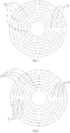
FIG. 1 is a schematic view of an LED substrate and package. -
FIG. 2 is a schematic view of an LED substrate and package. -
FIG. 3 is a schematic view of an LED substrate and package. -
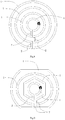
FIG. 4 is a schematic view of an LED substrate and package according to the present invention. -
FIG. 5 is a schematic view of the LED substrate and package according to the present invention after stretching. -
FIG. 6 is a schematic view of a connection between the connecting element on the LED substrate and package according to an embodiment of the present invention and the substrate. -
FIG. 7 is a schematic view of an LED substrate and package. -
FIG. 8 is a schematic view of an LED substrate and package. -
FIG. 9 is a schematic view of an LED substrate and package. -
FIG. 10 is a schematic view of an LED substrate and package. -
FIG. 11 is a schematic view of an LED substrate and package. -
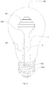
FIG. 12 is a schematic view of an LED bulb. -
FIG. 13 is a schematic view of an LED bulb. - The present invention will be further described in detail below with reference to the embodiments and drawings.
- As illustrated in
Figure 1 , the LED substrate comprises a plurality ofannular substrates 1 spaced apart from each other and concentrically arranged on the same plane, the plurality ofannular substrates 1 are circular and spaced apart from each other, and the radii of the plurality ofannular substrates 1 are gradually increased, and the spacing between theannular substrates 1 are the same or different. Every two adjacentannular substrates 1 are connected with each other by aconnection part 2. As shown inFigure 1 , only oneconnection part 2 is provided between two adjacent annular substrates, and the plurality ofconnection parts 2 are integrally connected with each other. A plurality of LED chips are connected in series and/or in parallel on theannular substrate 1. The plurality of LED chips can be electrically connected by connecting wires or electrically connected by circuits reserved on the annular substrate. The LED package is formed by the LED chips and the connecting wires between the LED chips disposed on the LED substrate. -
Figure 2 illustrates an LED substrate and package, which also comprises a plurality ofannular substrates 1 spaced apart from each other and arranged concentrically, and the connection parts are further provided between the plurality ofannular substrates 1. Every two adjacent annular substrates are connected with each other by twoconnection parts 2, and the twoconnection parts 2 between the plurality ofannular substrates 1 respectively correspond in position. -
Figure 3 illustrates an LED substrate and package wherein the LED substrate also comprises a plurality ofannular substrates 1 spaced apart from each other and arranged concentrically. Every two adjacentannular substrates 1 are connected with each other by fourconnection parts 2, and the fourconnection parts 2 between the plurality ofannular substrates 1 respectively correspond in position. -
Figure 4 illustrates an LED substrate and package according to the invention wherein the LED substrate also comprises a plurality ofannular substrates 1 spaced apart from each other and arranged concentrically, twoconnection parts 2, i.e. afirst connection part 21 and asecond connection part 22, are provided between adjacentannular substrates 1. Thefirst connection part 21 is a bending structure, thesecond connection part 22 includes a connectingelement 3 for disconnecting eachannular substrate 1 and a connectingmember 222 between a plurality of connectingelements 3. The connectingmember 222 is a bending structure, such that the connecting member has a smaller area and volume without reshaping and stretching, and has a greater length after reshaping and stretching. - As shown in
Figure 5 , the plurality ofannular substrates 1 are sequentially arranged in a three-dimensional structure from top to bottom and at a certain distance, as long as thefirst connection part 21 and the connectingmembers 222 between the plurality of connectingmembers 3 are reshaped. InFigure 5 , each annular substrate is in the same plane, and a plurality ofannular substrates 1 are respectively arranged in a plurality of planes parallel to each other. Alternatively, the plurality ofannular substrates 1 are respectively located on a plurality of planes which are not parallel or some of which parallel to each other, as long as theannular substrates 1 are respectively located in different planes. By means of such a substrate structure, when the planar substrate is to be fixed to a three-dimensional structure, it is only required toreshape and stretch the connectingmember 222 and thefirst connection part 21. That is, the substrate of three-dimensional structure is formed only by reshaping the connection part, such that the LED chips arranged on the substrate can achieve a multilevel and multi-angle lighting, and will not be easily damaged when reshping to the three-dimensional structure. This can ensure the processing efficiency and yield of the LED substrate. As shown inFigure 5 , the most medialannular substrate 1 is located at the top and the most lateralannular substrate 1 is located at the bottom. Alternatively, the most medial annular substrate is located at the bottom and the most lateral annular substrate is located at the top. Or the plurality ofannular substrates 1 are staggered with each other, that is, the plurality ofannular substrates 1 are arranged in a staggered manner in the vertical direction. To achieve such a three-dimensional substrate shape, it is only required to reshape and stretch theconnection part 2. - As shown in
Figure 4 , eachannular substrate 1 has a disconnectedopening 10 on which a connectingelement 3 is mounted. The connectingelement 3 has a configuration as shown inFigure 6 and comprises anouter material 31 surrounding the parts of theannular substrate 1 at two ends of theopening 10, and aninner material 32 disposed in theouter material 31, and theinner material 32 is not in contact with both ends of theopening 10, the connectingmember 222 connects theinner material 32 of two adjacentannular substrates 1, and the connectingelement 3 and the connectingmember 222 form thesecond connection part 22. Theouter material 31 only is used for connecting theannular substrate 1 at two ends of theopening 10 of theannular substrate 1 and is made of non-conductive material, while theinner material 32 is made of conductive material and is used for electrically connecting with the connectingmember 222. Moreover, the conductiveinner material 32 is also electrically connected with the LED chips 100 on theannular substrate 1 by the connectingwire 200 to achieve various connection and control modes. Eachannular substrate 1 is provided with at least oneopening 10, some of theopenings 10 are only used to form an open circuit, some of the openings are connected by the connectingelement 3. When theopening 10 is provided, the ends of theopening 10 of theannular substrate 1 is acted as one of the electrode leads of the substrate. -
Figure 7 is a schematic view of an LED substrate and package wherein the substrate in this embodiment comprises a plurality of concentric and sequentially spacedannular substrates 1, each of the annular substrates is a circular ring, each of theannular substrates 1 in the first to third embodiments is a closed ring, and theannular substrate 1 in the fourth embodiment is provided with theopening 10, but thesecond connection part 22 is provided on theopening 10 to connect the two ends of theopening 10 of theannular substrate 1. In this embodiment, eachannular substrate 1 has anopening 10, theopening 10 of eachannular substrate 1 is located at a corresponding position. Aconnection part 2 is provided between the adjacentannular substrates 1, and theconnection part 2 connects one end of theannular substrate 1 at theopening 10. For example, as shown inFigure 7 , fourannular substrates 1 spaced apart from each other are respectively a firstannular substrate 11, a secondannular substrate 12, a thirdannular substrate 13 and a fourthannular substrate 14, and each ofannular substrates 1 has anopening 10. Theopening 10 of the firstannular substrate 11 has afirst end 111 and asecond end 112, and theopening 10 of the secondannular substrate 12 has afirst end 121 and asecond end 122, and theopening 10 of the thirdannular substrate 13 has afirst end 131 and asecond end 132. Theopening 10 of the fourthannular substrate 14 has afirst end 141 and asecond end 142. Aconnection part 2 is connected between thefirst end 111 of theopening 10 of the firstannular substrate 11 and thefirst end 121 of theopening 10 of the secondannular substrate 12; aconnection part 2 is connected between thesecond end 122 of theopening 10 of the secondannular substrate 12 and thesecond end 132 of theopening 10 of the thirdannular substrate 13; and aconnection part 2 is connected between thefirst end 131 of theopening 10 of the thirdannular substrate 13 and thefirst end 141 of theopening 10 of the fourthannular substrate 14. That is, theconnection part 2 between the adjacentannular substrates 1 sequentially connects the plurality ofannular substrates 1 from end to end. That is to say, theconnection parts 2 between every two adjacentannular substrates 1 are not connected to each other and are not in the same position. That is, the connection part connects one end of the opening of the two adjacent annular substrates, and the two ends of theopening 10 of eachannular substrate 1 are respectively connected to the ends of theopenings 10 of twoannular substrates 1 adjacent to said annular substrate through different connection parts. -
Figure 8 is a schematic view of an LED substrate and package in which the configuration of substrate is substantially the same as that infigure 7 , except that theconnection part 2 is a bending structure, which makes the stretching and reshaping of theconnection part 2 more convenient, and the connection part is not easy to be damaged. Moreover, when a plurality of annular substrates are in the same plane, the distance between the annular substrates is smaller, which facilitates the processing and material saving. - As shown in
Figure 9 , the basic structure of an LED substrate and package in the seventh embodiment is the same as that infigures 7 and8 , except that each of theannular substrates 1 is not necessarily a circular ring structure, and some of theannular substrates 1 are polygonal ring structures, some of the annular substrates are circular ring structures, some of the annular substrates are annular structure composed of several arcs and several straight lines, such as a racetrack, and other irregular annular structures etc.. Theannular substrates 1 can be selected from a variety of other annular structures, as long as the annular substrates are spaced apart from each other. Moreover, although theannular substrates 1 in the above embodiments are all concentrically arranged, actually as long as theannular substrates 1 are spaced apart from each other, the above functions are also achieved by eccentrically arranging the annular substrates. Furthermore, the above functions are also achieved by arranging concentrically some of the annular substrates, and by eccentrically arranging annular substrates some of the annular substrates. Theannular substrates 1 are nested with each other when they are in the same plane. -
Figure 10 illustrates an LED substrate and package, which are different from those in the above embodiments. Theannular substrates 1 in this embodiment are in the same plane and are spaced apart from each other, except that theannular substrates 1 are not nested with each other, but sequentially separated from each other; every two adjacentannular substrates 1 are connected with each other by aconnection part 2. Moreover, eachannular substrate 1 is a circular ring and has the same diameter. As long as theconnection part 2 is reshaped, the plurality ofannular substrates 1 are reshaped into different planes, so as to obtain a multilevel and multi-surface light emitting three-dimensional structure. - As shown in
Figure 11 , like in the embodiment shown infigure 10 , theannular substrates 1 are disposed in the same plane and spaced apart from each other, and theannular substrates 1 are not nested with each other, but sequentially separated from each other. Every two adjacentannular substrates 1 are connected to each other by aconnection part 2. The ring diameter of theannular substrate 1 sequentially increases. As long as theconnection part 2 is reshaped, the plurality ofannular substrates 1 are transformed into different planes so as to obtain a multilevel and multi-surface light emitting three-dimensional structure. -
Figure 12 shows an LED bulb which comprises an outertransparent shell 300 and anLED package 400 disposed in thetransparent shell 300. Astem 500 with alead wire 8 and astem exhaust pipe 9 is disposed in thetransparent shell 300, and at least oneLED package 400 is fixed on thelead wire 8, the bottom of thetransparent shell 300 and the bottom of thestem 500 are fixed on anelectrical connector 600. Adriver 700 is disposed in theelectrical connector 600, and thelead wire 8 is connected to thedriver 700. In a sealed space formed by the transparent shell 20, a gas protecting the three-dimensional LED package and facilitating the heat dissipation of the three-dimensional LED package is filled, and the gas is helium gas or hydrogen-helium mixture gas. Thetransparent shell 300 is a transparent, milky white, frosted, or colored shell, and can also be a shell that is partly reflective or has small prisms and lens. The shape of thetransparent shell 300 is one of A-type, G-type, R-type, PAR-type, T-type, candle type or other shapes of existing bulbs. The electrical connector 90 is one of the existing electrical connectors such as E40, E27, E26, E14, and GU etc. TheLED package 400 in this embodiment is the LED package inFigure 1 . -
Figure 13 illustrates an LED bulb in which the structure of the LED bulb is substantially the same as that infigure 12 , except that twoLED packages 400 are disposed on thelead wire 300, and the two LED packages are arranged oppositely, so that the twoLED packages 400 form a three-dimensional shape that gradually increases and gradually decreases from top to bottom and in the radial direction. The twoLED packages 400 can be connected by theconnection part 2, or be connected by the connectingelement 3, and can also be electrically or structurally connected by other connecting mechanism. This structure makes the whole LED bulb have greater light emitting angle, more light emitting levels, and better three-dimensional effect. Moreover, theLED package 400 in this embodiment also is the LED package in the first embodiment. - By means of the multilevel light emitting LED substrate, package and bulb, a planar LED substrate and package can be transformed to be a three-dimensional structure; the manufacturing is convenient, the structure is simple, and it is easy to dispose and control LED chips; moreover, the process efficiency is high, so that the LED package is not easily to be damaged in the process, and the production efficiency and yield are improved.
- The scope of the invention is defined by the claims.
Claims (9)
- A multilevel light emitting LED substrate comprising a plurality of annular substrates (1) spaced apart from each other wherein every two adjacent annular substrates (1) among the plurality of annular substrates (1) are connected with each other by using at least one connection part (2), the plurality of annular substrates (1) are located in different planes to form a three-dimensional structure by stretching and reshaping the connection part (2), characterized in that each of the plurality of annular substrates (1) is provided with a disconnected opening (10) and in that a connecting element (3) is disposed on the opening (10), the connecting element (3) comprises an outer material (31) wrapping and connecting two ends of the opening (10), an inner material (32) located in the outer material (31) and without contacting with two ends of the opening (10), the outer material (31) is made of non-conductive material and the inner material (32) is made of conductive material, the inner material (32) is electrically connected with the LED chips (100) on the annular substrate (1) by a connecting wire (200).
- The multilevel light emitting LED substrate according to claim 1, characterized in that there is one connection part(2) between every two adjacent annular substrates (1), and the connection parts (2) are connected with each other and the positions thereof correspond to each other.
- The multilevel light emitting LED substrate according to claim 1, characterized in that a connecting member (222) is connected between the inner materials (32) of the connecting elements (3) of each annular substrates (1).
- The multilevel light emitting LED substrate according to claim 1 or 2, characterized in that the connecting member (222) and/or the connection part (2) are/is a bending structure.
- The multilevel light emitting LED substrate according to any of the preceding claims, characterized in that the annular substrate (1) is a polygonal annular structure, a circular ring structure, or an annular structure composed of several arcs and several straight lines.
- The multilevel light emitting LED substrate according to claim 1, characterized in that the connection part (2) connects one end of the openings (10) of two adjacent annular substrates respectively, and the two ends of the opening (10) of each annular substrate (1) are respectively connected with the ends of the openings (10) of two annular substrates (1) adjacent to said annular substrate by means of different connection parts (2).
- The multilevel light emitting LED substrate according to claim 1, characterized in that the plurality of annular substrates (1) are nested with each other, and the plurality of annular substrates are concentrically or eccentrically arranged; or the plurality of annular substrates (1) are arranged next to and separately from each other.
- A multilayered light emitting LED package, comprising the light emitting LED substrate according to any one of claims 1-7, characterized in that a plurality of LED chips are arranged in series and/or in parallel on the annular substrate (1).
- A multilayered light emitting LED bulb having the multilayered light emitting LED package according to claim 8, characterized in that, comprising an outer transparent shell (300) and a stem (500) disposed in the transparent shell (300), the stem is provided with a lead wire (8) on which at least one LED package (400) is fixed, an electrical connector (600) is disposed at the bottom of the transparent shell (300) and the bottom of the stem (500), a driver (700) is disposed in the electrical connector (600), and the lead wire (8) is connected to the driver (700).
Applications Claiming Priority (4)
| Application Number | Priority Date | Filing Date | Title |
|---|---|---|---|
| CN201520703575.XU CN204927353U (en) | 2015-09-11 | 2015-09-11 | Multi -level luminous LED base plate |
| CN201520701064.4U CN205001877U (en) | 2015-09-11 | 2015-09-11 | Multi -level luminous LED encapsulation |
| CN201520701453.7U CN205001884U (en) | 2015-09-11 | 2015-09-11 | Multi -level luminous LED bulb |
| PCT/CN2016/098299 WO2017041709A1 (en) | 2015-09-11 | 2016-09-07 | Multilevel light emitting led substrate and package, and bulb |
Publications (3)
| Publication Number | Publication Date |
|---|---|
| EP3349261A1 EP3349261A1 (en) | 2018-07-18 |
| EP3349261A4 EP3349261A4 (en) | 2018-08-01 |
| EP3349261B1 true EP3349261B1 (en) | 2019-04-24 |
Family
ID=58240134
Family Applications (1)
| Application Number | Title | Priority Date | Filing Date |
|---|---|---|---|
| EP16843647.5A Active EP3349261B1 (en) | 2015-09-11 | 2016-09-07 | Multilevel light emitting led substrate and package, and bulb |
Country Status (4)
| Country | Link |
|---|---|
| US (1) | US10269719B2 (en) |
| EP (1) | EP3349261B1 (en) |
| CA (1) | CA2996499C (en) |
| WO (1) | WO2017041709A1 (en) |
Families Citing this family (1)
| Publication number | Priority date | Publication date | Assignee | Title |
|---|---|---|---|---|
| US11452265B2 (en) * | 2020-12-05 | 2022-09-27 | Lettuce Grow by TFP, LLC | Lighting system for vertical garden |
Family Cites Families (9)
| Publication number | Priority date | Publication date | Assignee | Title |
|---|---|---|---|---|
| TWI434006B (en) * | 2011-11-30 | 2014-04-11 | Ind Tech Res Inst | Lighting device |
| CN203463969U (en) | 2013-06-09 | 2014-03-05 | 北京半导体照明科技促进中心 | LED stereo light source |
| CN203656627U (en) | 2013-12-02 | 2014-06-18 | 张晓峰 | Lamp bulb with one spiral LED lamp filament |
| CN204176377U (en) * | 2014-10-15 | 2015-02-25 | 杨志强 | Three-dimensional LED packaged light bulb |
| CN204927353U (en) | 2015-09-11 | 2015-12-30 | 葛铁汉 | Multi -level luminous LED base plate |
| CN105098050B (en) | 2015-09-11 | 2019-03-01 | 葛铁汉 | A kind of multi-level light-emitting LED substrate |
| CN205001877U (en) | 2015-09-11 | 2016-01-27 | 葛铁汉 | Multi -level luminous LED encapsulation |
| CN205001884U (en) | 2015-09-11 | 2016-01-27 | 葛铁汉 | Multi -level luminous LED bulb |
| CN205065341U (en) | 2015-10-29 | 2016-03-02 | 苏州紫昱天成光电有限公司 | LED lamp filament |
-
2016
- 2016-09-07 EP EP16843647.5A patent/EP3349261B1/en active Active
- 2016-09-07 CA CA2996499A patent/CA2996499C/en active Active
- 2016-09-07 US US15/757,713 patent/US10269719B2/en active Active
- 2016-09-07 WO PCT/CN2016/098299 patent/WO2017041709A1/en not_active Ceased
Non-Patent Citations (1)
| Title |
|---|
| None * |
Also Published As
| Publication number | Publication date |
|---|---|
| US20180337132A1 (en) | 2018-11-22 |
| US10269719B2 (en) | 2019-04-23 |
| EP3349261A4 (en) | 2018-08-01 |
| EP3349261A1 (en) | 2018-07-18 |
| WO2017041709A1 (en) | 2017-03-16 |
| CA2996499C (en) | 2021-07-27 |
| CA2996499A1 (en) | 2017-03-16 |
Similar Documents
| Publication | Publication Date | Title |
|---|---|---|
| EP3065174B1 (en) | Spiral led filament and light bulb using spiral led filament | |
| EP3812647B1 (en) | Filament structure and bulb having the filament structure | |
| JP3175918U (en) | Improved structure of light-emitting diode bulb | |
| JP2017532793A (en) | Substrate used for LED sealing, three-dimensional LED sealing body, light bulb having three-dimensional LED sealing body, and manufacturing method thereof | |
| CN203656627U (en) | Lamp bulb with one spiral LED lamp filament | |
| KR20120078560A (en) | Light emitting diode lamp and method for fabricating the same | |
| WO2017028740A1 (en) | Substrate for led packaging, led package, and led bulb | |
| JP3187458U (en) | Light emitting diode bulb | |
| US20170030557A1 (en) | Optical structure | |
| TW201621210A (en) | LED light source and light fixture | |
| US20140153236A1 (en) | Light emitting diode bulb | |
| EP3805628B1 (en) | Novel led filament | |
| CN205001912U (en) | Space multi -angle LED bulb that gives out light; give off light | |
| CN205001884U (en) | Multi -level luminous LED bulb | |
| US10269719B2 (en) | Multilevel light emitting LED substrate, package and bulb | |
| US20140198495A1 (en) | LED Bulb Laterally Installed and Projecting Light Beams onto Ground | |
| CN205065326U (en) | Flexible base plate LED aerifys lamp | |
| CN205001877U (en) | Multi -level luminous LED encapsulation | |
| JP6839701B2 (en) | Lighting equipment with flexible circuit strips wrapped around a support | |
| CN205001878U (en) | Luminous LED encapsulation of space multi -angle | |
| CN204240103U (en) | Bulb of spiral LED encapsulation | |
| EP3699481B1 (en) | Lamp | |
| WO2017041710A1 (en) | Led substrate for spatial multi-angle light emission, package, and lamp bulb | |
| TWM523810U (en) | LED light source and lamp | |
| CN105098050A (en) | Multi-level luminous light-emitting diode (LED) substrate |
Legal Events
| Date | Code | Title | Description |
|---|---|---|---|
| STAA | Information on the status of an ep patent application or granted ep patent |
Free format text: STATUS: THE INTERNATIONAL PUBLICATION HAS BEEN MADE |
|
| PUAI | Public reference made under article 153(3) epc to a published international application that has entered the european phase |
Free format text: ORIGINAL CODE: 0009012 |
|
| STAA | Information on the status of an ep patent application or granted ep patent |
Free format text: STATUS: REQUEST FOR EXAMINATION WAS MADE |
|
| 17P | Request for examination filed |
Effective date: 20180212 |
|
| AK | Designated contracting states |
Kind code of ref document: A1 Designated state(s): AL AT BE BG CH CY CZ DE DK EE ES FI FR GB GR HR HU IE IS IT LI LT LU LV MC MK MT NL NO PL PT RO RS SE SI SK SM TR |
|
| AX | Request for extension of the european patent |
Extension state: BA ME |
|
| A4 | Supplementary search report drawn up and despatched |
Effective date: 20180629 |
|
| RIC1 | Information provided on ipc code assigned before grant |
Ipc: F21K 9/20 20160101ALI20180625BHEP Ipc: F21Y 115/10 20160101ALN20180625BHEP Ipc: F21Y 107/40 20160101ALN20180625BHEP Ipc: F21K 9/232 20160101ALI20180625BHEP Ipc: H01L 33/64 20100101AFI20180625BHEP Ipc: F21Y 107/50 20160101ALN20180625BHEP |
|
| GRAP | Despatch of communication of intention to grant a patent |
Free format text: ORIGINAL CODE: EPIDOSNIGR1 |
|
| STAA | Information on the status of an ep patent application or granted ep patent |
Free format text: STATUS: GRANT OF PATENT IS INTENDED |
|
| DAV | Request for validation of the european patent (deleted) | ||
| DAX | Request for extension of the european patent (deleted) | ||
| RIC1 | Information provided on ipc code assigned before grant |
Ipc: F21K 9/232 20160101ALI20181109BHEP Ipc: F21Y 107/50 20160101ALN20181109BHEP Ipc: F21K 9/20 20160101ALI20181109BHEP Ipc: F21Y 115/10 20160101ALN20181109BHEP Ipc: H01L 33/64 20100101AFI20181109BHEP Ipc: F21Y 107/40 20160101ALN20181109BHEP |
|
| RIC1 | Information provided on ipc code assigned before grant |
Ipc: F21K 9/232 20160101ALI20181127BHEP Ipc: F21K 9/20 20160101ALI20181127BHEP Ipc: F21Y 107/50 20160101ALN20181127BHEP Ipc: F21Y 115/10 20160101ALN20181127BHEP Ipc: H01L 33/64 20100101AFI20181127BHEP Ipc: F21Y 107/40 20160101ALN20181127BHEP |
|
| INTG | Intention to grant announced |
Effective date: 20181212 |
|
| GRAS | Grant fee paid |
Free format text: ORIGINAL CODE: EPIDOSNIGR3 |
|
| GRAA | (expected) grant |
Free format text: ORIGINAL CODE: 0009210 |
|
| STAA | Information on the status of an ep patent application or granted ep patent |
Free format text: STATUS: THE PATENT HAS BEEN GRANTED |
|
| AK | Designated contracting states |
Kind code of ref document: B1 Designated state(s): AL AT BE BG CH CY CZ DE DK EE ES FI FR GB GR HR HU IE IS IT LI LT LU LV MC MK MT NL NO PL PT RO RS SE SI SK SM TR |
|
| REG | Reference to a national code |
Ref country code: GB Ref legal event code: FG4D |
|
| REG | Reference to a national code |
Ref country code: CH Ref legal event code: EP |
|
| REG | Reference to a national code |
Ref country code: AT Ref legal event code: REF Ref document number: 1125184 Country of ref document: AT Kind code of ref document: T Effective date: 20190515 Ref country code: IE Ref legal event code: FG4D |
|
| REG | Reference to a national code |
Ref country code: DE Ref legal event code: R096 Ref document number: 602016012984 Country of ref document: DE |
|
| REG | Reference to a national code |
Ref country code: NL Ref legal event code: FP |
|
| REG | Reference to a national code |
Ref country code: LT Ref legal event code: MG4D |
|
| PG25 | Lapsed in a contracting state [announced via postgrant information from national office to epo] |
Ref country code: SE Free format text: LAPSE BECAUSE OF FAILURE TO SUBMIT A TRANSLATION OF THE DESCRIPTION OR TO PAY THE FEE WITHIN THE PRESCRIBED TIME-LIMIT Effective date: 20190424 Ref country code: HR Free format text: LAPSE BECAUSE OF FAILURE TO SUBMIT A TRANSLATION OF THE DESCRIPTION OR TO PAY THE FEE WITHIN THE PRESCRIBED TIME-LIMIT Effective date: 20190424 Ref country code: AL Free format text: LAPSE BECAUSE OF FAILURE TO SUBMIT A TRANSLATION OF THE DESCRIPTION OR TO PAY THE FEE WITHIN THE PRESCRIBED TIME-LIMIT Effective date: 20190424 Ref country code: PT Free format text: LAPSE BECAUSE OF FAILURE TO SUBMIT A TRANSLATION OF THE DESCRIPTION OR TO PAY THE FEE WITHIN THE PRESCRIBED TIME-LIMIT Effective date: 20190824 Ref country code: FI Free format text: LAPSE BECAUSE OF FAILURE TO SUBMIT A TRANSLATION OF THE DESCRIPTION OR TO PAY THE FEE WITHIN THE PRESCRIBED TIME-LIMIT Effective date: 20190424 Ref country code: NO Free format text: LAPSE BECAUSE OF FAILURE TO SUBMIT A TRANSLATION OF THE DESCRIPTION OR TO PAY THE FEE WITHIN THE PRESCRIBED TIME-LIMIT Effective date: 20190724 Ref country code: LT Free format text: LAPSE BECAUSE OF FAILURE TO SUBMIT A TRANSLATION OF THE DESCRIPTION OR TO PAY THE FEE WITHIN THE PRESCRIBED TIME-LIMIT Effective date: 20190424 Ref country code: ES Free format text: LAPSE BECAUSE OF FAILURE TO SUBMIT A TRANSLATION OF THE DESCRIPTION OR TO PAY THE FEE WITHIN THE PRESCRIBED TIME-LIMIT Effective date: 20190424 |
|
| PG25 | Lapsed in a contracting state [announced via postgrant information from national office to epo] |
Ref country code: GR Free format text: LAPSE BECAUSE OF FAILURE TO SUBMIT A TRANSLATION OF THE DESCRIPTION OR TO PAY THE FEE WITHIN THE PRESCRIBED TIME-LIMIT Effective date: 20190725 Ref country code: BG Free format text: LAPSE BECAUSE OF FAILURE TO SUBMIT A TRANSLATION OF THE DESCRIPTION OR TO PAY THE FEE WITHIN THE PRESCRIBED TIME-LIMIT Effective date: 20190724 Ref country code: RS Free format text: LAPSE BECAUSE OF FAILURE TO SUBMIT A TRANSLATION OF THE DESCRIPTION OR TO PAY THE FEE WITHIN THE PRESCRIBED TIME-LIMIT Effective date: 20190424 Ref country code: PL Free format text: LAPSE BECAUSE OF FAILURE TO SUBMIT A TRANSLATION OF THE DESCRIPTION OR TO PAY THE FEE WITHIN THE PRESCRIBED TIME-LIMIT Effective date: 20190424 Ref country code: LV Free format text: LAPSE BECAUSE OF FAILURE TO SUBMIT A TRANSLATION OF THE DESCRIPTION OR TO PAY THE FEE WITHIN THE PRESCRIBED TIME-LIMIT Effective date: 20190424 |
|
| REG | Reference to a national code |
Ref country code: AT Ref legal event code: MK05 Ref document number: 1125184 Country of ref document: AT Kind code of ref document: T Effective date: 20190424 |
|
| PG25 | Lapsed in a contracting state [announced via postgrant information from national office to epo] |
Ref country code: IS Free format text: LAPSE BECAUSE OF FAILURE TO SUBMIT A TRANSLATION OF THE DESCRIPTION OR TO PAY THE FEE WITHIN THE PRESCRIBED TIME-LIMIT Effective date: 20190824 |
|
| REG | Reference to a national code |
Ref country code: DE Ref legal event code: R097 Ref document number: 602016012984 Country of ref document: DE |
|
| PG25 | Lapsed in a contracting state [announced via postgrant information from national office to epo] |
Ref country code: DK Free format text: LAPSE BECAUSE OF FAILURE TO SUBMIT A TRANSLATION OF THE DESCRIPTION OR TO PAY THE FEE WITHIN THE PRESCRIBED TIME-LIMIT Effective date: 20190424 Ref country code: EE Free format text: LAPSE BECAUSE OF FAILURE TO SUBMIT A TRANSLATION OF THE DESCRIPTION OR TO PAY THE FEE WITHIN THE PRESCRIBED TIME-LIMIT Effective date: 20190424 Ref country code: AT Free format text: LAPSE BECAUSE OF FAILURE TO SUBMIT A TRANSLATION OF THE DESCRIPTION OR TO PAY THE FEE WITHIN THE PRESCRIBED TIME-LIMIT Effective date: 20190424 Ref country code: RO Free format text: LAPSE BECAUSE OF FAILURE TO SUBMIT A TRANSLATION OF THE DESCRIPTION OR TO PAY THE FEE WITHIN THE PRESCRIBED TIME-LIMIT Effective date: 20190424 Ref country code: CZ Free format text: LAPSE BECAUSE OF FAILURE TO SUBMIT A TRANSLATION OF THE DESCRIPTION OR TO PAY THE FEE WITHIN THE PRESCRIBED TIME-LIMIT Effective date: 20190424 Ref country code: SK Free format text: LAPSE BECAUSE OF FAILURE TO SUBMIT A TRANSLATION OF THE DESCRIPTION OR TO PAY THE FEE WITHIN THE PRESCRIBED TIME-LIMIT Effective date: 20190424 |
|
| PG25 | Lapsed in a contracting state [announced via postgrant information from national office to epo] |
Ref country code: SM Free format text: LAPSE BECAUSE OF FAILURE TO SUBMIT A TRANSLATION OF THE DESCRIPTION OR TO PAY THE FEE WITHIN THE PRESCRIBED TIME-LIMIT Effective date: 20190424 Ref country code: IT Free format text: LAPSE BECAUSE OF FAILURE TO SUBMIT A TRANSLATION OF THE DESCRIPTION OR TO PAY THE FEE WITHIN THE PRESCRIBED TIME-LIMIT Effective date: 20190424 |
|
| PLBE | No opposition filed within time limit |
Free format text: ORIGINAL CODE: 0009261 |
|
| STAA | Information on the status of an ep patent application or granted ep patent |
Free format text: STATUS: NO OPPOSITION FILED WITHIN TIME LIMIT |
|
| PG25 | Lapsed in a contracting state [announced via postgrant information from national office to epo] |
Ref country code: TR Free format text: LAPSE BECAUSE OF FAILURE TO SUBMIT A TRANSLATION OF THE DESCRIPTION OR TO PAY THE FEE WITHIN THE PRESCRIBED TIME-LIMIT Effective date: 20190424 |
|
| 26N | No opposition filed |
Effective date: 20200127 |
|
| PG25 | Lapsed in a contracting state [announced via postgrant information from national office to epo] |
Ref country code: MC Free format text: LAPSE BECAUSE OF FAILURE TO SUBMIT A TRANSLATION OF THE DESCRIPTION OR TO PAY THE FEE WITHIN THE PRESCRIBED TIME-LIMIT Effective date: 20190424 |
|
| REG | Reference to a national code |
Ref country code: CH Ref legal event code: PL |
|
| PG25 | Lapsed in a contracting state [announced via postgrant information from national office to epo] |
Ref country code: LI Free format text: LAPSE BECAUSE OF NON-PAYMENT OF DUE FEES Effective date: 20190930 Ref country code: LU Free format text: LAPSE BECAUSE OF NON-PAYMENT OF DUE FEES Effective date: 20190907 Ref country code: CH Free format text: LAPSE BECAUSE OF NON-PAYMENT OF DUE FEES Effective date: 20190930 Ref country code: IE Free format text: LAPSE BECAUSE OF NON-PAYMENT OF DUE FEES Effective date: 20190907 |
|
| PG25 | Lapsed in a contracting state [announced via postgrant information from national office to epo] |
Ref country code: CY Free format text: LAPSE BECAUSE OF FAILURE TO SUBMIT A TRANSLATION OF THE DESCRIPTION OR TO PAY THE FEE WITHIN THE PRESCRIBED TIME-LIMIT Effective date: 20190424 |
|
| PG25 | Lapsed in a contracting state [announced via postgrant information from national office to epo] |
Ref country code: HU Free format text: LAPSE BECAUSE OF FAILURE TO SUBMIT A TRANSLATION OF THE DESCRIPTION OR TO PAY THE FEE WITHIN THE PRESCRIBED TIME-LIMIT; INVALID AB INITIO Effective date: 20160907 Ref country code: MT Free format text: LAPSE BECAUSE OF FAILURE TO SUBMIT A TRANSLATION OF THE DESCRIPTION OR TO PAY THE FEE WITHIN THE PRESCRIBED TIME-LIMIT Effective date: 20190424 |
|
| PG25 | Lapsed in a contracting state [announced via postgrant information from national office to epo] |
Ref country code: SI Free format text: LAPSE BECAUSE OF FAILURE TO SUBMIT A TRANSLATION OF THE DESCRIPTION OR TO PAY THE FEE WITHIN THE PRESCRIBED TIME-LIMIT Effective date: 20190424 |
|
| PG25 | Lapsed in a contracting state [announced via postgrant information from national office to epo] |
Ref country code: MK Free format text: LAPSE BECAUSE OF FAILURE TO SUBMIT A TRANSLATION OF THE DESCRIPTION OR TO PAY THE FEE WITHIN THE PRESCRIBED TIME-LIMIT Effective date: 20190424 |
|
| PGFP | Annual fee paid to national office [announced via postgrant information from national office to epo] |
Ref country code: BE Payment date: 20240919 Year of fee payment: 9 |
|
| PGFP | Annual fee paid to national office [announced via postgrant information from national office to epo] |
Ref country code: NL Payment date: 20240919 Year of fee payment: 9 |
|
| REG | Reference to a national code |
Ref country code: DE Ref legal event code: R079 Ref document number: 602016012984 Country of ref document: DE Free format text: PREVIOUS MAIN CLASS: H01L0033640000 Ipc: H10H0020858000 |
|
| PGFP | Annual fee paid to national office [announced via postgrant information from national office to epo] |
Ref country code: DE Payment date: 20250929 Year of fee payment: 10 |
|
| PGFP | Annual fee paid to national office [announced via postgrant information from national office to epo] |
Ref country code: GB Payment date: 20250930 Year of fee payment: 10 |
|
| PGFP | Annual fee paid to national office [announced via postgrant information from national office to epo] |
Ref country code: FR Payment date: 20250930 Year of fee payment: 10 |
|
| REG | Reference to a national code |
Ref country code: NL Ref legal event code: MM Effective date: 20251001 |