EP3349251B1 - High efficiency solar cell and method for manufacturing high efficiency solar cell - Google Patents
High efficiency solar cell and method for manufacturing high efficiency solar cell Download PDFInfo
- Publication number
- EP3349251B1 EP3349251B1 EP16886815.6A EP16886815A EP3349251B1 EP 3349251 B1 EP3349251 B1 EP 3349251B1 EP 16886815 A EP16886815 A EP 16886815A EP 3349251 B1 EP3349251 B1 EP 3349251B1
- Authority
- EP
- European Patent Office
- Prior art keywords
- solar cell
- base
- emitter
- insulator film
- region
- Prior art date
- Legal status (The legal status is an assumption and is not a legal conclusion. Google has not performed a legal analysis and makes no representation as to the accuracy of the status listed.)
- Active
Links
- 238000000034 method Methods 0.000 title claims description 38
- 238000004519 manufacturing process Methods 0.000 title claims description 17
- 239000012212 insulator Substances 0.000 claims description 84
- 239000000758 substrate Substances 0.000 claims description 59
- 229920001721 polyimide Polymers 0.000 claims description 36
- 239000004642 Polyimide Substances 0.000 claims description 30
- 239000004065 semiconductor Substances 0.000 claims description 27
- 150000002500 ions Chemical class 0.000 claims description 22
- 125000003178 carboxy group Chemical group [H]OC(*)=O 0.000 claims description 20
- XUIMIQQOPSSXEZ-UHFFFAOYSA-N Silicon Chemical compound [Si] XUIMIQQOPSSXEZ-UHFFFAOYSA-N 0.000 claims description 19
- 229910052710 silicon Inorganic materials 0.000 claims description 19
- 239000010703 silicon Substances 0.000 claims description 19
- 239000013078 crystal Substances 0.000 claims description 12
- 238000001514 detection method Methods 0.000 claims description 10
- 238000005011 time of flight secondary ion mass spectroscopy Methods 0.000 claims description 10
- 238000010248 power generation Methods 0.000 claims description 9
- 230000001133 acceleration Effects 0.000 claims description 6
- 238000002161 passivation Methods 0.000 description 13
- 239000002243 precursor Substances 0.000 description 13
- 239000002904 solvent Substances 0.000 description 12
- 239000002253 acid Substances 0.000 description 10
- 238000010438 heat treatment Methods 0.000 description 10
- 238000002042 time-of-flight secondary ion mass spectrometry Methods 0.000 description 9
- 238000006243 chemical reaction Methods 0.000 description 8
- ZMXDDKWLCZADIW-UHFFFAOYSA-N N,N-Dimethylformamide Chemical compound CN(C)C=O ZMXDDKWLCZADIW-UHFFFAOYSA-N 0.000 description 7
- 239000011248 coating agent Substances 0.000 description 7
- 238000009413 insulation Methods 0.000 description 7
- 238000007650 screen-printing Methods 0.000 description 7
- 239000000126 substance Substances 0.000 description 6
- 150000001408 amides Chemical class 0.000 description 5
- 230000000052 comparative effect Effects 0.000 description 5
- 238000001723 curing Methods 0.000 description 5
- 230000003247 decreasing effect Effects 0.000 description 5
- 238000006116 polymerization reaction Methods 0.000 description 5
- 239000000843 powder Substances 0.000 description 5
- 229910052581 Si3N4 Inorganic materials 0.000 description 4
- 238000000576 coating method Methods 0.000 description 4
- 239000009719 polyimide resin Substances 0.000 description 4
- CYIDZMCFTVVTJO-UHFFFAOYSA-N pyromellitic acid Chemical compound OC(=O)C1=CC(C(O)=O)=C(C(O)=O)C=C1C(O)=O CYIDZMCFTVVTJO-UHFFFAOYSA-N 0.000 description 4
- HQVNEWCFYHHQES-UHFFFAOYSA-N silicon nitride Chemical compound N12[Si]34N5[Si]62N3[Si]51N64 HQVNEWCFYHHQES-UHFFFAOYSA-N 0.000 description 4
- 239000007790 solid phase Substances 0.000 description 4
- 238000012360 testing method Methods 0.000 description 4
- 150000000000 tetracarboxylic acids Chemical class 0.000 description 4
- FXHOOIRPVKKKFG-UHFFFAOYSA-N N,N-Dimethylacetamide Chemical compound CN(C)C(C)=O FXHOOIRPVKKKFG-UHFFFAOYSA-N 0.000 description 3
- SECXISVLQFMRJM-UHFFFAOYSA-N N-Methylpyrrolidone Chemical compound CN1CCCC1=O SECXISVLQFMRJM-UHFFFAOYSA-N 0.000 description 3
- VYPSYNLAJGMNEJ-UHFFFAOYSA-N Silicium dioxide Chemical compound O=[Si]=O VYPSYNLAJGMNEJ-UHFFFAOYSA-N 0.000 description 3
- 230000015572 biosynthetic process Effects 0.000 description 3
- 238000009792 diffusion process Methods 0.000 description 3
- 230000000694 effects Effects 0.000 description 3
- 238000005259 measurement Methods 0.000 description 3
- 229920005575 poly(amic acid) Polymers 0.000 description 3
- 229910052814 silicon oxide Inorganic materials 0.000 description 3
- -1 tetracarboxylic diester Chemical class 0.000 description 3
- 229920001187 thermosetting polymer Polymers 0.000 description 3
- 229910052724 xenon Inorganic materials 0.000 description 3
- FHNFHKCVQCLJFQ-UHFFFAOYSA-N xenon atom Chemical compound [Xe] FHNFHKCVQCLJFQ-UHFFFAOYSA-N 0.000 description 3
- RNLHGQLZWXBQNY-UHFFFAOYSA-N 3-(aminomethyl)-3,5,5-trimethylcyclohexan-1-amine Chemical compound CC1(C)CC(N)CC(C)(CN)C1 RNLHGQLZWXBQNY-UHFFFAOYSA-N 0.000 description 2
- RTZKZFJDLAIYFH-UHFFFAOYSA-N Diethyl ether Chemical compound CCOCC RTZKZFJDLAIYFH-UHFFFAOYSA-N 0.000 description 2
- ATUOYWHBWRKTHZ-UHFFFAOYSA-N Propane Chemical compound CCC ATUOYWHBWRKTHZ-UHFFFAOYSA-N 0.000 description 2
- 238000010521 absorption reaction Methods 0.000 description 2
- ILAHWRKJUDSMFH-UHFFFAOYSA-N boron tribromide Chemical compound BrB(Br)Br ILAHWRKJUDSMFH-UHFFFAOYSA-N 0.000 description 2
- 150000001732 carboxylic acid derivatives Chemical class 0.000 description 2
- 238000005229 chemical vapour deposition Methods 0.000 description 2
- 239000006059 cover glass Substances 0.000 description 2
- 150000004985 diamines Chemical class 0.000 description 2
- 238000001035 drying Methods 0.000 description 2
- 238000005227 gel permeation chromatography Methods 0.000 description 2
- 239000011521 glass Substances 0.000 description 2
- 238000007641 inkjet printing Methods 0.000 description 2
- 239000000203 mixture Substances 0.000 description 2
- 239000011347 resin Substances 0.000 description 2
- 229920005989 resin Polymers 0.000 description 2
- 150000003839 salts Chemical class 0.000 description 2
- 238000001228 spectrum Methods 0.000 description 2
- 239000012808 vapor phase Substances 0.000 description 2
- GXVUZYLYWKWJIM-UHFFFAOYSA-N 2-(2-aminoethoxy)ethanamine Chemical compound NCCOCCN GXVUZYLYWKWJIM-UHFFFAOYSA-N 0.000 description 1
- XUSNPFGLKGCWGN-UHFFFAOYSA-N 3-[4-(3-aminopropyl)piperazin-1-yl]propan-1-amine Chemical compound NCCCN1CCN(CCCN)CC1 XUSNPFGLKGCWGN-UHFFFAOYSA-N 0.000 description 1
- LFBALUPVVFCEPA-UHFFFAOYSA-N 4-(3,4-dicarboxyphenyl)phthalic acid Chemical compound C1=C(C(O)=O)C(C(=O)O)=CC=C1C1=CC=C(C(O)=O)C(C(O)=O)=C1 LFBALUPVVFCEPA-UHFFFAOYSA-N 0.000 description 1
- HLBLWEWZXPIGSM-UHFFFAOYSA-N 4-Aminophenyl ether Chemical compound C1=CC(N)=CC=C1OC1=CC=C(N)C=C1 HLBLWEWZXPIGSM-UHFFFAOYSA-N 0.000 description 1
- APXJLYIVOFARRM-UHFFFAOYSA-N 4-[2-(3,4-dicarboxyphenyl)-1,1,1,3,3,3-hexafluoropropan-2-yl]phthalic acid Chemical compound C1=C(C(O)=O)C(C(=O)O)=CC=C1C(C(F)(F)F)(C(F)(F)F)C1=CC=C(C(O)=O)C(C(O)=O)=C1 APXJLYIVOFARRM-UHFFFAOYSA-N 0.000 description 1
- HHLMWQDRYZAENA-UHFFFAOYSA-N 4-[4-[2-[4-(4-aminophenoxy)phenyl]-1,1,1,3,3,3-hexafluoropropan-2-yl]phenoxy]aniline Chemical compound C1=CC(N)=CC=C1OC1=CC=C(C(C=2C=CC(OC=3C=CC(N)=CC=3)=CC=2)(C(F)(F)F)C(F)(F)F)C=C1 HHLMWQDRYZAENA-UHFFFAOYSA-N 0.000 description 1
- 229910015845 BBr3 Inorganic materials 0.000 description 1
- ZPAKUZKMGJJMAA-UHFFFAOYSA-N Cyclohexane-1,2,4,5-tetracarboxylic acid Chemical compound OC(=O)C1CC(C(O)=O)C(C(O)=O)CC1C(O)=O ZPAKUZKMGJJMAA-UHFFFAOYSA-N 0.000 description 1
- QLBRROYTTDFLDX-UHFFFAOYSA-N [3-(aminomethyl)cyclohexyl]methanamine Chemical compound NCC1CCCC(CN)C1 QLBRROYTTDFLDX-UHFFFAOYSA-N 0.000 description 1
- 238000004458 analytical method Methods 0.000 description 1
- 229910052787 antimony Inorganic materials 0.000 description 1
- WATWJIUSRGPENY-UHFFFAOYSA-N antimony atom Chemical compound [Sb] WATWJIUSRGPENY-UHFFFAOYSA-N 0.000 description 1
- 229910052785 arsenic Inorganic materials 0.000 description 1
- RQNWIZPPADIBDY-UHFFFAOYSA-N arsenic atom Chemical compound [As] RQNWIZPPADIBDY-UHFFFAOYSA-N 0.000 description 1
- 239000012298 atmosphere Substances 0.000 description 1
- QVGXLLKOCUKJST-UHFFFAOYSA-N atomic oxygen Chemical compound [O] QVGXLLKOCUKJST-UHFFFAOYSA-N 0.000 description 1
- 239000011230 binding agent Substances 0.000 description 1
- 229910052797 bismuth Inorganic materials 0.000 description 1
- JCXGWMGPZLAOME-UHFFFAOYSA-N bismuth atom Chemical compound [Bi] JCXGWMGPZLAOME-UHFFFAOYSA-N 0.000 description 1
- DQXBYHZEEUGOBF-UHFFFAOYSA-N but-3-enoic acid;ethene Chemical compound C=C.OC(=O)CC=C DQXBYHZEEUGOBF-UHFFFAOYSA-N 0.000 description 1
- 230000008878 coupling Effects 0.000 description 1
- 238000010168 coupling process Methods 0.000 description 1
- 238000005859 coupling reaction Methods 0.000 description 1
- 238000006297 dehydration reaction Methods 0.000 description 1
- 150000005690 diesters Chemical class 0.000 description 1
- 150000002148 esters Chemical class 0.000 description 1
- JBTWLSYIZRCDFO-UHFFFAOYSA-N ethyl methyl carbonate Chemical compound CCOC(=O)OC JBTWLSYIZRCDFO-UHFFFAOYSA-N 0.000 description 1
- 239000005038 ethylene vinyl acetate Substances 0.000 description 1
- 239000000945 filler Substances 0.000 description 1
- BHEPBYXIRTUNPN-UHFFFAOYSA-N hydridophosphorus(.) (triplet) Chemical compound [PH] BHEPBYXIRTUNPN-UHFFFAOYSA-N 0.000 description 1
- 230000001678 irradiating effect Effects 0.000 description 1
- 150000002576 ketones Chemical class 0.000 description 1
- 238000000608 laser ablation Methods 0.000 description 1
- 239000000463 material Substances 0.000 description 1
- OJURWUUOVGOHJZ-UHFFFAOYSA-N methyl 2-[(2-acetyloxyphenyl)methyl-[2-[(2-acetyloxyphenyl)methyl-(2-methoxy-2-oxoethyl)amino]ethyl]amino]acetate Chemical compound C=1C=CC=C(OC(C)=O)C=1CN(CC(=O)OC)CCN(CC(=O)OC)CC1=CC=CC=C1OC(C)=O OJURWUUOVGOHJZ-UHFFFAOYSA-N 0.000 description 1
- 238000002156 mixing Methods 0.000 description 1
- 230000003287 optical effect Effects 0.000 description 1
- 230000003647 oxidation Effects 0.000 description 1
- 238000007254 oxidation reaction Methods 0.000 description 1
- 239000001301 oxygen Substances 0.000 description 1
- 229910052760 oxygen Inorganic materials 0.000 description 1
- 230000002093 peripheral effect Effects 0.000 description 1
- 125000001997 phenyl group Chemical group [H]C1=C([H])C([H])=C(*)C([H])=C1[H] 0.000 description 1
- XHXFXVLFKHQFAL-UHFFFAOYSA-N phosphoryl trichloride Chemical compound ClP(Cl)(Cl)=O XHXFXVLFKHQFAL-UHFFFAOYSA-N 0.000 description 1
- 238000005268 plasma chemical vapour deposition Methods 0.000 description 1
- 238000007747 plating Methods 0.000 description 1
- 229920001200 poly(ethylene-vinyl acetate) Polymers 0.000 description 1
- 229920000139 polyethylene terephthalate Polymers 0.000 description 1
- 239000005020 polyethylene terephthalate Substances 0.000 description 1
- 229920000098 polyolefin Polymers 0.000 description 1
- 229920001451 polypropylene glycol Polymers 0.000 description 1
- 229920001296 polysiloxane Polymers 0.000 description 1
- 239000001294 propane Substances 0.000 description 1
- 230000007261 regionalization Effects 0.000 description 1
- 239000005361 soda-lime glass Substances 0.000 description 1
- 239000007787 solid Substances 0.000 description 1
- XLYOFNOQVPJJNP-UHFFFAOYSA-N water Substances O XLYOFNOQVPJJNP-UHFFFAOYSA-N 0.000 description 1
Images


Classifications
-
- H—ELECTRICITY
- H01—ELECTRIC ELEMENTS
- H01L—SEMICONDUCTOR DEVICES NOT COVERED BY CLASS H10
- H01L31/00—Semiconductor devices sensitive to infrared radiation, light, electromagnetic radiation of shorter wavelength or corpuscular radiation and specially adapted either for the conversion of the energy of such radiation into electrical energy or for the control of electrical energy by such radiation; Processes or apparatus specially adapted for the manufacture or treatment thereof or of parts thereof; Details thereof
- H01L31/02—Details
- H01L31/0224—Electrodes
- H01L31/022408—Electrodes for devices characterised by at least one potential jump barrier or surface barrier
- H01L31/022425—Electrodes for devices characterised by at least one potential jump barrier or surface barrier for solar cells
- H01L31/022441—Electrode arrangements specially adapted for back-contact solar cells
-
- C—CHEMISTRY; METALLURGY
- C08—ORGANIC MACROMOLECULAR COMPOUNDS; THEIR PREPARATION OR CHEMICAL WORKING-UP; COMPOSITIONS BASED THEREON
- C08G—MACROMOLECULAR COMPOUNDS OBTAINED OTHERWISE THAN BY REACTIONS ONLY INVOLVING UNSATURATED CARBON-TO-CARBON BONDS
- C08G73/00—Macromolecular compounds obtained by reactions forming a linkage containing nitrogen with or without oxygen or carbon in the main chain of the macromolecule, not provided for in groups C08G12/00 - C08G71/00
- C08G73/06—Polycondensates having nitrogen-containing heterocyclic rings in the main chain of the macromolecule
- C08G73/10—Polyimides; Polyester-imides; Polyamide-imides; Polyamide acids or similar polyimide precursors
- C08G73/1003—Preparatory processes
- C08G73/1007—Preparatory processes from tetracarboxylic acids or derivatives and diamines
- C08G73/1028—Preparatory processes from tetracarboxylic acids or derivatives and diamines characterised by the process itself, e.g. steps, continuous
- C08G73/1032—Preparatory processes from tetracarboxylic acids or derivatives and diamines characterised by the process itself, e.g. steps, continuous characterised by the solvent(s) used
-
- G—PHYSICS
- G01—MEASURING; TESTING
- G01N—INVESTIGATING OR ANALYSING MATERIALS BY DETERMINING THEIR CHEMICAL OR PHYSICAL PROPERTIES
- G01N23/00—Investigating or analysing materials by the use of wave or particle radiation, e.g. X-rays or neutrons, not covered by groups G01N3/00 – G01N17/00, G01N21/00 or G01N22/00
- G01N23/22—Investigating or analysing materials by the use of wave or particle radiation, e.g. X-rays or neutrons, not covered by groups G01N3/00 – G01N17/00, G01N21/00 or G01N22/00 by measuring secondary emission from the material
- G01N23/225—Investigating or analysing materials by the use of wave or particle radiation, e.g. X-rays or neutrons, not covered by groups G01N3/00 – G01N17/00, G01N21/00 or G01N22/00 by measuring secondary emission from the material using electron or ion
- G01N23/2255—Investigating or analysing materials by the use of wave or particle radiation, e.g. X-rays or neutrons, not covered by groups G01N3/00 – G01N17/00, G01N21/00 or G01N22/00 by measuring secondary emission from the material using electron or ion using incident ion beams, e.g. proton beams
- G01N23/2258—Measuring secondary ion emission, e.g. secondary ion mass spectrometry [SIMS]
-
- H—ELECTRICITY
- H01—ELECTRIC ELEMENTS
- H01L—SEMICONDUCTOR DEVICES NOT COVERED BY CLASS H10
- H01L31/00—Semiconductor devices sensitive to infrared radiation, light, electromagnetic radiation of shorter wavelength or corpuscular radiation and specially adapted either for the conversion of the energy of such radiation into electrical energy or for the control of electrical energy by such radiation; Processes or apparatus specially adapted for the manufacture or treatment thereof or of parts thereof; Details thereof
- H01L31/02—Details
- H01L31/0216—Coatings
- H01L31/02161—Coatings for devices characterised by at least one potential jump barrier or surface barrier
- H01L31/02167—Coatings for devices characterised by at least one potential jump barrier or surface barrier for solar cells
-
- H—ELECTRICITY
- H01—ELECTRIC ELEMENTS
- H01L—SEMICONDUCTOR DEVICES NOT COVERED BY CLASS H10
- H01L31/00—Semiconductor devices sensitive to infrared radiation, light, electromagnetic radiation of shorter wavelength or corpuscular radiation and specially adapted either for the conversion of the energy of such radiation into electrical energy or for the control of electrical energy by such radiation; Processes or apparatus specially adapted for the manufacture or treatment thereof or of parts thereof; Details thereof
- H01L31/02—Details
- H01L31/0224—Electrodes
- H01L31/022408—Electrodes for devices characterised by at least one potential jump barrier or surface barrier
- H01L31/022425—Electrodes for devices characterised by at least one potential jump barrier or surface barrier for solar cells
- H01L31/022441—Electrode arrangements specially adapted for back-contact solar cells
- H01L31/02245—Electrode arrangements specially adapted for back-contact solar cells for metallisation wrap-through [MWT] type solar cells
-
- H—ELECTRICITY
- H01—ELECTRIC ELEMENTS
- H01L—SEMICONDUCTOR DEVICES NOT COVERED BY CLASS H10
- H01L31/00—Semiconductor devices sensitive to infrared radiation, light, electromagnetic radiation of shorter wavelength or corpuscular radiation and specially adapted either for the conversion of the energy of such radiation into electrical energy or for the control of electrical energy by such radiation; Processes or apparatus specially adapted for the manufacture or treatment thereof or of parts thereof; Details thereof
- H01L31/0248—Semiconductor devices sensitive to infrared radiation, light, electromagnetic radiation of shorter wavelength or corpuscular radiation and specially adapted either for the conversion of the energy of such radiation into electrical energy or for the control of electrical energy by such radiation; Processes or apparatus specially adapted for the manufacture or treatment thereof or of parts thereof; Details thereof characterised by their semiconductor bodies
- H01L31/036—Semiconductor devices sensitive to infrared radiation, light, electromagnetic radiation of shorter wavelength or corpuscular radiation and specially adapted either for the conversion of the energy of such radiation into electrical energy or for the control of electrical energy by such radiation; Processes or apparatus specially adapted for the manufacture or treatment thereof or of parts thereof; Details thereof characterised by their semiconductor bodies characterised by their crystalline structure or particular orientation of the crystalline planes
-
- H—ELECTRICITY
- H01—ELECTRIC ELEMENTS
- H01L—SEMICONDUCTOR DEVICES NOT COVERED BY CLASS H10
- H01L31/00—Semiconductor devices sensitive to infrared radiation, light, electromagnetic radiation of shorter wavelength or corpuscular radiation and specially adapted either for the conversion of the energy of such radiation into electrical energy or for the control of electrical energy by such radiation; Processes or apparatus specially adapted for the manufacture or treatment thereof or of parts thereof; Details thereof
- H01L31/04—Semiconductor devices sensitive to infrared radiation, light, electromagnetic radiation of shorter wavelength or corpuscular radiation and specially adapted either for the conversion of the energy of such radiation into electrical energy or for the control of electrical energy by such radiation; Processes or apparatus specially adapted for the manufacture or treatment thereof or of parts thereof; Details thereof adapted as photovoltaic [PV] conversion devices
- H01L31/042—PV modules or arrays of single PV cells
- H01L31/05—Electrical interconnection means between PV cells inside the PV module, e.g. series connection of PV cells
- H01L31/0504—Electrical interconnection means between PV cells inside the PV module, e.g. series connection of PV cells specially adapted for series or parallel connection of solar cells in a module
- H01L31/0516—Electrical interconnection means between PV cells inside the PV module, e.g. series connection of PV cells specially adapted for series or parallel connection of solar cells in a module specially adapted for interconnection of back-contact solar cells
-
- H—ELECTRICITY
- H01—ELECTRIC ELEMENTS
- H01L—SEMICONDUCTOR DEVICES NOT COVERED BY CLASS H10
- H01L31/00—Semiconductor devices sensitive to infrared radiation, light, electromagnetic radiation of shorter wavelength or corpuscular radiation and specially adapted either for the conversion of the energy of such radiation into electrical energy or for the control of electrical energy by such radiation; Processes or apparatus specially adapted for the manufacture or treatment thereof or of parts thereof; Details thereof
- H01L31/04—Semiconductor devices sensitive to infrared radiation, light, electromagnetic radiation of shorter wavelength or corpuscular radiation and specially adapted either for the conversion of the energy of such radiation into electrical energy or for the control of electrical energy by such radiation; Processes or apparatus specially adapted for the manufacture or treatment thereof or of parts thereof; Details thereof adapted as photovoltaic [PV] conversion devices
- H01L31/06—Semiconductor devices sensitive to infrared radiation, light, electromagnetic radiation of shorter wavelength or corpuscular radiation and specially adapted either for the conversion of the energy of such radiation into electrical energy or for the control of electrical energy by such radiation; Processes or apparatus specially adapted for the manufacture or treatment thereof or of parts thereof; Details thereof adapted as photovoltaic [PV] conversion devices characterised by at least one potential-jump barrier or surface barrier
- H01L31/068—Semiconductor devices sensitive to infrared radiation, light, electromagnetic radiation of shorter wavelength or corpuscular radiation and specially adapted either for the conversion of the energy of such radiation into electrical energy or for the control of electrical energy by such radiation; Processes or apparatus specially adapted for the manufacture or treatment thereof or of parts thereof; Details thereof adapted as photovoltaic [PV] conversion devices characterised by at least one potential-jump barrier or surface barrier the potential barriers being only of the PN homojunction type, e.g. bulk silicon PN homojunction solar cells or thin film polycrystalline silicon PN homojunction solar cells
- H01L31/0682—Semiconductor devices sensitive to infrared radiation, light, electromagnetic radiation of shorter wavelength or corpuscular radiation and specially adapted either for the conversion of the energy of such radiation into electrical energy or for the control of electrical energy by such radiation; Processes or apparatus specially adapted for the manufacture or treatment thereof or of parts thereof; Details thereof adapted as photovoltaic [PV] conversion devices characterised by at least one potential-jump barrier or surface barrier the potential barriers being only of the PN homojunction type, e.g. bulk silicon PN homojunction solar cells or thin film polycrystalline silicon PN homojunction solar cells back-junction, i.e. rearside emitter, solar cells, e.g. interdigitated base-emitter regions back-junction cells
-
- H—ELECTRICITY
- H01—ELECTRIC ELEMENTS
- H01L—SEMICONDUCTOR DEVICES NOT COVERED BY CLASS H10
- H01L31/00—Semiconductor devices sensitive to infrared radiation, light, electromagnetic radiation of shorter wavelength or corpuscular radiation and specially adapted either for the conversion of the energy of such radiation into electrical energy or for the control of electrical energy by such radiation; Processes or apparatus specially adapted for the manufacture or treatment thereof or of parts thereof; Details thereof
- H01L31/18—Processes or apparatus specially adapted for the manufacture or treatment of these devices or of parts thereof
- H01L31/1804—Processes or apparatus specially adapted for the manufacture or treatment of these devices or of parts thereof comprising only elements of Group IV of the Periodic System
-
- H—ELECTRICITY
- H01—ELECTRIC ELEMENTS
- H01L—SEMICONDUCTOR DEVICES NOT COVERED BY CLASS H10
- H01L31/00—Semiconductor devices sensitive to infrared radiation, light, electromagnetic radiation of shorter wavelength or corpuscular radiation and specially adapted either for the conversion of the energy of such radiation into electrical energy or for the control of electrical energy by such radiation; Processes or apparatus specially adapted for the manufacture or treatment thereof or of parts thereof; Details thereof
- H01L31/02—Details
- H01L31/0224—Electrodes
- H01L31/022408—Electrodes for devices characterised by at least one potential jump barrier or surface barrier
- H01L31/022425—Electrodes for devices characterised by at least one potential jump barrier or surface barrier for solar cells
- H01L31/022441—Electrode arrangements specially adapted for back-contact solar cells
- H01L31/022458—Electrode arrangements specially adapted for back-contact solar cells for emitter wrap-through [EWT] type solar cells, e.g. interdigitated emitter-base back-contacts
-
- H—ELECTRICITY
- H01—ELECTRIC ELEMENTS
- H01L—SEMICONDUCTOR DEVICES NOT COVERED BY CLASS H10
- H01L31/00—Semiconductor devices sensitive to infrared radiation, light, electromagnetic radiation of shorter wavelength or corpuscular radiation and specially adapted either for the conversion of the energy of such radiation into electrical energy or for the control of electrical energy by such radiation; Processes or apparatus specially adapted for the manufacture or treatment thereof or of parts thereof; Details thereof
- H01L31/18—Processes or apparatus specially adapted for the manufacture or treatment of these devices or of parts thereof
-
- Y—GENERAL TAGGING OF NEW TECHNOLOGICAL DEVELOPMENTS; GENERAL TAGGING OF CROSS-SECTIONAL TECHNOLOGIES SPANNING OVER SEVERAL SECTIONS OF THE IPC; TECHNICAL SUBJECTS COVERED BY FORMER USPC CROSS-REFERENCE ART COLLECTIONS [XRACs] AND DIGESTS
- Y02—TECHNOLOGIES OR APPLICATIONS FOR MITIGATION OR ADAPTATION AGAINST CLIMATE CHANGE
- Y02E—REDUCTION OF GREENHOUSE GAS [GHG] EMISSIONS, RELATED TO ENERGY GENERATION, TRANSMISSION OR DISTRIBUTION
- Y02E10/00—Energy generation through renewable energy sources
- Y02E10/50—Photovoltaic [PV] energy
- Y02E10/547—Monocrystalline silicon PV cells
Definitions
- the present invention relates to a high efficiency solar cell and a method for manufacturing a high efficiency solar cell.
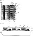
- FIG. 11 is a schematic view showing an example of the back surface of the back contact solar cell
- FIG. 12 shows a part of a cross section taken along an alternate long and short dash line A in FIG. 11 .
- an emitter region (an emitter layer) 1112 is formed on the back surface (a first main surface) of a semiconductor substrate (e.g., a crystal silicon substrate) 1110.
- base regions (base layers) 1113 are formed in a stripe pattern to sandwich the emitter region 1112 therebetween
- emitter electrodes 1122 are formed on the emitter region 1112, and further a plurality of emitter electrodes 1122 are coupled through emitter bus bars (emitter bus bar electrodes) 1132.
- base electrodes 1123 are formed on the base regions 1113, and a plurality of base electrodes 1123 are coupled through base bus bars (base bus bar electrodes) 1133.
- the base electrodes 1123 are electrically insulated from the emitter region 1112 through insulator films (insulator layers) 1118 and the emitter electrodes 1122 are electrically insulated from the base regions 1113 through the same.
- the solar cell 1100 includes passivation films 1119 on the first main surface and a second main surface of the semiconductor substrate 1110. It is to be noted that the passivation film 1119 is omitted in FIG. 11 .
- a material used for the insulator films must have characteristics such as chemical stableness, high usable temperatures, or easiness of pattern formation.
- a polyimide resin has been often used for the insulator film due to such demands (e.g., Patent Literature and EP-A1-2273558 ).
- the insulator film of the solar cell is formed by applying an insulation precursor (an insulator film precursor) to the substrate by screen printing, inkjet printing, or a dispensing method.
- an insulation precursor an insulator film precursor
- a solution containing a polyamic acid is generally used as a precursor in case of applying a polyimide resin for formation.
- the polyamic acid is thermally treated to advance dehydration reaction and imidization, whereby the polyimide resin is provided.
- Patent Literature 1 Japanese Unexamined Patent Application Publication No. 2015-26858
- the present invention has been made in view of the above problems, and an object thereof is to provide a solar cell which has excellent weather resistance and high photoelectric conversion characteristics and a method for manufacturing such a solar cell.
- the present invention provides a solar cell comprising: a semiconductor substrate having a first conductivity type; an emitter region, having a second conductivity type opposite to the first conductivity type, on a first main surface of the semiconductor substrate; an emitter electrode which is in contact with the emitter region; a base region having the first conductivity type; a base electrode which is in contact with the base region; and an insulator film for preventing an electrical short-circuit between the emitter region and the base region, wherein the insulator film is made of a polyimide containing no carboxy group, and the insulator film has a C 6 H 11 O 2 detection count number of 100 or less when the insulator film is irradiated with Bi 5 ++ ions at an acceleration voltage of 30 kV and an ion current of 0.2 pA by a TOF-SIMS method.
- Such a solar cell is superior in weather resistance and has high photoelectric conversion characteristics.
- the insulator film is formed to electrically insulate the emitter region from the base electrode.
- Such a solar cell can avoid the electrical short-circuit of the emitter region and the base electrode by using the insulator film.
- the insulator film is formed to electrically insulate the base region from the emitter electrode.
- Such a solar cell can avoid the electrical short-circuit of the base region and the emitter electrode by using the insulator film.
- the insulator film is formed to electrically insulate the emitter electrode from the base electrode.
- Such a solar cell can avoid the electrical short-circuit of the emitter electrode and the base electrode by using the insulator film.
- the semiconductor substrate is a crystal silicon substrate.
- the semiconductor substrate is the crystal silicon substrate
- the solar cell which has good power generation efficiency can be provided at low cost.
- the present invention provides a photovoltaic module including solar cells according to the present invention electrically connected to each other.
- the solar cells according to the present invention can be electrically connected to provide the photovoltaic module.
- the present invention provides a photovoltaic power generation system including a plurality of photovoltaic modules according to the present invention connected to each other.
- the plurality of photovoltaic modules each of which is constituted by electrically connecting the solar cells according to the present invention can be connected to provide the photovoltaic power generation system.
- the present invention provides a method for manufacturing a solar cell comprising the steps of:
- a crystal silicon substrate as the semiconductor substrate.
- the method according to the present invention is particularly preferable for manufacture of the solar cell including the crystal silicon substrate.
- the solar cell of the present invention is superior in weather resistance and has high photoelectric conversion characteristics. According to the method of the present invention, it is possible to provide a back contact solar cell which has high efficiency and excellent weather resistance without requiring a process change.
- a solar cell including: a semiconductor substrate having a first conductivity type; an emitter region, having a second conductivity type opposite to the first conductivity type, on a first main surface of the semiconductor substrate; an emitter electrode which is in contact with the emitter region; a base region having the first conductivity type; a base electrode which is in contact with the base region; and an insulator film for preventing an electrical short-circuit between the emitter region and the base region, wherein the insulator film is made of a polyimide, containing no carboxy group and the insulator film has a C 6 H 11 O 2 detection count number of 100 or less when the insulator film is irradiated with Bi 5 ++ ions at an acceleration voltage of 30 kV and an ion current of 0.2 pA by a TOF-SIMS method, thereby bringing the present invention to completion.
- the present inventors have conducted the earnest examinations to achieve the object. Consequently, they have found that the problem can be solved by a method for manufacturing a solar cell including the steps of:
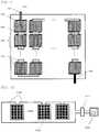
- FIG. 1 is a view showing a backside structure of a back contact solar cell according to the present invention.
- FIG. 2 is a view showing a cross-sectional structure of the back contact solar cell according to the present invention, and shows a part of a cross section taken along an alternate long and short dash line A in FIG. 1 .
- a solar cell 100 according to the present invention includes a semiconductor substrate 110 having a first conductivity type.
- an emitter region 112 having a second conductivity type opposite to the first conductivity type emitter electrodes 122 which are in contact with the emitter region 112
- base regions 113 having the first conductivity type base electrodes 123 which are in contact with the base regions 113
- insulator films 118 which prevent an electrical short-circuit between the emitter region 112 and the base regions 113.
- the solar cell 100 usually includes base bus bars 133 configured to further collect currents which can be provided from the base electrodes 123. Additionally, it usually includes emitter bus bars 132 configured to further collect currents which can be provided from the emitter electrodes 122. Further, as shown in FIG. 2 , passivation films 119 are usually provided on the first main surface and a second main surface of the semiconductor substrate 110. It is to be noted that the passivation film 119 is omitted in FIG. 1 .
- the insulator film 118 is made of a polyimide and has a C 6 H 11 O 2 detection count number of 100 or less when the insulator film 118 is irradiated with Bi 5 ++ ions (divalent ions of a bismuth pentamer) at an acceleration voltage of 30 kV and an ion current of 0.2 pA (picoampere) by a time-of-flight secondary ion mass spectrometry (TOF-SIMS) method.
- This detection count number is approximately a detection lower limit of the TOF-SIMS.
- an organic substance containing a carboxy group can be detected as, e.g., a peak of C 6 H 11 O 2 whose m/z value (m: an ion mass number, z: an ion charge number) appears in the vicinity of 115 in secondary ions ejected by Bi ion irradiation in the TOS-SIMS.
- each insulator film is made of a polyimide which hardly contains carboxy groups or does not contain the same at all.
- a carboxylic acid is generated from the carboxy group derived from an amic acid with moisture absorption of the insulator film and acts on electrodes themselves or an interface between the electrodes and silicon to degrade electric resistance.
- the shape of the insulator film is not restricted in particular, it may be, e.g., a rectangular shape.
- the length of one side of the insulator film may be, e.g., 0.01 mm to 50 mm.
- the thickness of the insulator film may be, e.g., 1 to 60 ⁇ m. Adopting such length and thickness enables further improving insulation properties.
- the insulator films are not excessively formed, it is possible to assuredly manufacture a desired solar cell, namely, a solar cell in which each insulator film is made of a polyimide containing no carboxy group.
- the solar cell 100 it is preferable to form the solar cell 100 according to the present invention so that the insulator films 118 electrically insulate the emitter region 112 from the base electrodes 123.
- the insulator films 118 electrically insulate the emitter region 112 from the base electrodes 123.
- Such a solar cell enables avoiding an electrical short-circuit between the emitter region and the base electrodes by using the insulator films.
- the solar cell 100 it is preferable to form the solar cell 100 according to the present invention so that the insulator films 118 electrically insulate the base regions 113 from the emitter electrodes 122.
- Such a solar cell enables avoiding an electrical short-circuit between the base regions and the emitter electrodes.
- the solar cell 100 it is preferable to form the solar cell 100 according to the present invention so that the insulator films 118 electrically insulate the emitter electrodes 122 from the base electrodes 123.
- Such a solar cell enables avoiding an electrical short-circuit between the emitter electrodes and the base electrodes.
- the semiconductor substrate 110 is a crystal silicon substrate.
- the semiconductor substrate is the crystal silicon substrate in this manner, the solar cell with the good power generation efficiency can be provided at low costs.
- the method according to the present invention can be applied to general solar cells using insulators, an example of the method will now be described.
- the method according to the present invention can be applied to the solar cell shown in FIGS. 1 and 2 .
- a specific method for manufacturing a solar cell will be described with reference to FIGS. 1 and 2 in conjunction with a case using an N-type substrate.
- an N-type semiconductor substrate such as an N-type crystal silicon substrate is prepared.
- high-purity silicon may be doped with a pentad such as phosphorous, arsenic, or antimony to prepare an as-cut single crystal ⁇ 100 ⁇ N-type silicon substrate having a specific resistance of 0.1 to 5 ⁇ cm.
- small irregularities called a texture may be formed on a light receiving surface of the semiconductor substrate to reduce reflectance of the solar cell.
- an emitter region 112 having a second conductivity type opposite to that of the semiconductor substrate 110 and base regions 113 having a first conductivity type equal to that of the semiconductor substrate 110 are formed on the back surface (a first main surface) of the semiconductor substrate 110.
- a method for forming the emitter region 112 and the base regions 113 is not restricted in particular, and a well-known method can be used.
- the emitter region 112 can be formed by vapor phase diffusion using BBr 3 or the like.
- the base regions 113 can be formed by vapor phase diffusion using phosphorous oxychloride.
- a diffusion mask composed of a silicon oxide film, a silicon nitride film, or the like may be used to form the emitter region 112 and the base regions 113 with desired shapes.
- a diffusion mask composed of a silicon oxide film, a silicon nitride film, or the like may be used to form the emitter region 112 and the base regions 113 with desired shapes.
- stripe-shaped base regions 113 may be formed, while emitter region 112 are formed except for areas where the base regions 113 are formed.
- a passivation film 119 constituted of a silicon nitride film, a silicon oxide film, or the like is formed on each of the light receiving surface and the back surface of the semiconductor substrate 110.
- the silicon nitride film can be formed by a CVD method, and the silicon oxide film can be formed by the CVD method or a thermal oxidation method.
- emitter electrodes 122 which are in contact with the emitter region 112, and base electrodes 123 which are in contact with the base regions 113 are formed.
- the emitter electrodes 122 and the base electrodes 123 which extend in a horizontal direction are formed on the emitter region 112 and the base regions 113.
- the emitter electrodes 122 and the base electrodes 123 are formed as follows: an Ag paste obtained by mixing Ag powder and glass frit with an organic binder is applied to the emitter region 112 and the base regions 113 with the passivation film 119 being inserted; the Ag paste is then dried; and the Ag paste is fired at about 700 to 880°C for 1 to 30 minutes. As a result of this heat treatment, the passivation film 119 is eroded by the Ag paste, whereby the electrodes make electrical contact with the silicon.
- plating may be applied.
- the passivation film 119 at such positions is removed by, e.g., laser ablation.
- the insulator films 118 for preventing an electrical short-circuit between the emitter region 112 and the base regions 113.
- the insulator films 118 are formed at intersecting points of the emitter region 112 and base bus bars 133 and intersecting points of the base regions 113 and emitter bus bars 132.
- the film is preferably formed by applying a paste of an insulation precursor by screen printing, inkjet printing, or dispensed coating in terms of productivity.
- a process differs to some extent depending on the insulation precursor to be used, it is often the case that the precursor is printed and thereafter dried in the air at approximately 70°C to 150°C for approximately one minute to 10 minutes, and then an actual curing is performed.
- an actual curing method also varies depending on the insulation precursor, it may be a thermosetting type, a UV (ultraviolet) curing type, or the like.
- heat treatment conditions for performing the actual curing for example, heat treatment can be carried out in the air at 200°C to 400°C for approximately 10 seconds to 15 minutes.
- each insulator film 118 is made of a polyimide containing no carboxy group.
- an organic substance containing carboxy groups can be detected as, e.g., a peak of C 6 H 11 O 2 whose m/z value (m: an ion mass number, z: an ion charge number) appears in the vicinity of 115 in secondary ions ejected by Bi ion irradiation in the TOS-SIMS.
- an actually cured insulator film having a C 6 H 11 O 2 detection count number of 100 or less when it is irradiated with Bi 5 ++ ions at an acceleration voltage of 30 kV and an ion current of 0.2 pA by the TOF-SIMS method can be regarded as the insulator film made of a polyimide containing no carboxy group. It is to be noted that the detection count number (100) is roughly a detection lower limit of the TOF-SIMS method.
- an amic acid solution is dehydrated/imidized by heat treatment, but imidization is partially incomplete due to a coating film thickness, heat treatment conditions, or the like, and the precursor remains in some situations. In such a case, there is a possibility that optimizing the coating film thickness and the heat treatment conditions can avoid the problem.
- an insulator film precursor containing no amic acid it is preferable to use an insulator film precursor containing no amic acid.
- a soluble polyimide coating agent using a soluble polyimide described in Japanese Unexamined Patent Application Publication No. 2015-180721 can be adopted.
- the soluble polyimide is, e.g., a polyimide powder provided by a solid phase polymerization method, and this polyimide can be the polyimide powder which is soluble in an amide solvent and whose weight-average molecular weight based on GPC (gel permeation chromatography) is 10000 or more.
- GPC gel permeation chromatography
- amide solvent examples include N-methyl-2-pyrolidone (NMP), N,N-dimethylformamide (DMF), N,N-dimethylacetamide (DMAc), and the like.
- the polyimide powder can be manufactured by solid-phase-polymerizing a salt consisting of a tetracarboxylic acid or a tetracarboxylic diester and diamine in the presence of a solvent in an amount of 1 mass% or more and 30 mass% or less with respect to a mass of this salt.
- the solid phase polymerization method is a method for advancing polymerization reaction in a solid state.
- the tetracarboxylic diester means a tetracarboxylic acid dimethyl ester, a tetracarboxylic acid diethyl ester, a tetracarboxylic diisopropyl acid ester, or the like.
- tetracarboxylic acid examples include cyclohexane-1,2,4,5-tetracarboxylic acid (H-PMA), pyromellitic acid (PMA), 3,3',4,4'-biphenyltetracarboxylic acid (BPA), 2,2-bis(3,4-dicarboxyphenyl) hexafluoropropane (6-FA), diesters of these substances, and the like.
- H-PMA cyclohexane-1,2,4,5-tetracarboxylic acid
- PMA pyromellitic acid
- BPA 3,3',4,4'-biphenyltetracarboxylic acid
- 6-FA 2,2-bis(3,4-dicarboxyphenyl) hexafluoropropane
- diamine examples include 4,4'-diaminodiphenyl ether (DADE), 2,2-bis[4-(4-aminophenyxy)phenyl]propane (BAPP), 1,3-bis(aminomethyl) cyclohexane (AMC), isophoronediamine (IPDA), 2,2-bis[4-(4-aminophenoxy)phenyl]hexafluoropropane (6F-BAPP), polypropylene glycol bis(2-aminoethyl) ether (PGAE), and the like.
- DADE 4,4'-diaminodiphenyl ether
- BAPP 2,2-bis[4-(4-aminophenyxy)phenyl]propane
- AMC 1,3-bis(aminomethyl) cyclohexane
- IPDA isophoronediamine
- 6F-BAPP 2,2-bis[4-(4-aminophenoxy)phenyl]hexafluoroprop
- the solvent used in the solid phase polymerization is a solvent which can dissolve the polyimide powder to be generated by the solid phase polymerization.
- Illustrative examples thereof include general solvents such as an amide solvent, an ether solvent, a water ester solvent, a ketone solvent, and the like; and the amide solvent is preferred.
- As the amide solvent, NMP, DMF, DMAc, or the like described above can be used.
- the sample A is an amic acid type polyimide film that is cured by, after coating and drying at 90°C for five minutes, heat treatment at 250°C for 10 minutes.
- the samples B to D are polyimide films made of soluble polyimides having different compositions, but a peak derived from the amic acid, which can be seen in the sample A, cannot be observed in these samples.
- Table 1 shows the details of the insulator films A, B, C, and D.
- Insulator film Film thickness Heat treatment conditions Type of insulator film precursor C 6 H 11 O 2 detection count number Composition of insulator film precursor (volume%) Resin component Solvent Others A about 20 ⁇ m drying at 90°C for 5 minutes, curing at 250°C for 10 minutes
- Amic acid solution about 1600 30 67 3
- the emitter bus bars 132 and the base bus bars 133 are formed.
- a thermosetting conductive paste which is curable at room temperature to 350°C or a UV curable conductive paste can be used for these bus bars, and such a paste could be applied by screen printing or dispenser formation.
- the insulator films 118 can electrically insulate the emitter electrodes 122 from the base bus bars 133 and also electrically insulate the base electrodes 123 from the emitter bus bars 132, while the emitter electrodes 122 and the emitter bus bars 132 can be configured to be electrically continuous, and the base electrodes 123 and the base bus bars 133 can be configured to be electrically continuous.
- the method of the present invention it is possible to provide a back contact solar cell having excellent durability and high efficiency.
- the foregoing examples are in conjunction with the case where the substrate is an N-type substrate, the method of the present invention can also be applied to a case where the substrate is a P-type substrate. That is, an N-type layer may be provided as an emitter layer while a P-type layer may be provided as a base layer.
- FIG. 4 is a view showing a back surface of an emitter-wrap-through solar cell 400 as a solar cell according to another embodiment of the present invention, and each of FIG. 5 (a cross-sectional view taken along an alternate long and short dash line A) and FIG. 6 (a cross-sectional view taken along an alternate long and short dash line B) shows a part of a cross section taken along the alternate long and short dash line A or B in FIG. 4 .
- the light receiving surface faces downward.
- a base region 113 and base electrodes 123 formed on the base region 113 most part of the back surface of a substrate 110 is occupied by a base region 113 and base electrodes 123 formed on the base region 113, and emitter regions 112 are formed into island shapes in regions sandwiched between insulator films 118.
- a light receiving surface is occupied by an emitter region 112 that communicates with the emitter regions 112 on the back surface through via holes opened in the substrate 110.
- emitter electrodes 122 are connected between the light-receiving surface and the back surface through the via holes.
- a passivation film 119 is formed on the light receiving surface.
- base bus bars 133 are linearly formed on the base electrode 123 on the back surface of the substrate 110.
- emitter bus bars 132 are linearly formed on the emitter regions 112 and the emitter electrodes 122 on the back surface of the substrate 110. However, as shown in FIG. 6 , in each region where the emitter bus bar 132 crosses the base electrode 123, the base electrode 123 is covered with the insulator film 118.
- FIG. 7 is a view showing the back surface of a solar cell 700 of still another embodiment according to the present invention
- FIG. 8 is a cross-sectional view showing a part of a cross section taken along an alternate long and short dash line A in FIG. 7
- base regions 113 on the back surface of a substrate 110 are formed in such a manner that they are surrounded by an emitter region 112, and each base electrode 123 is in contact with the base region 113 and insulated from a passivation film 119 through an insulator film 118 in a portion where the base electrode 123 overlaps the emitter region 112.
- the passivation film 119 is omitted in FIG. 7 . Additionally, at an outer peripheral portion of the back surface of the substrate 110, an emitter bus bar 132 which is coupled with a plurality of emitter electrodes 122 is formed, and a base bus bar 133 which is coupled with a plurality of base electrodes 123 is formed.
- each base region 113 is linearly formed below the base electrode 123, but the present invention is not restricted thereto, each base region 113 may be formed into a dot shape and these regions may be linearly aligned.
- the base electrodes 123 are formed in such a manner that they are insulated from the emitter region 112 through the insulator films 118 and connect the base regions 113.
- a photovoltaic module according to the present invention is constituted by electrically connecting the solar cells according to the present invention.
- a photovoltaic module is provided.
- FIG. 9 shows an example of a photovoltaic module 916.
- a positive electrode 923 of a solar cell is electrically connected to a negative electrode 922 of an adjacent solar cell through a tab 912, and the number of solar cells (solar battery cells) 900 required for a predetermined output are connected.
- the connected solar cells 900 are sealed with a cover glass, a filter, and further a back sheet.
- a soda-lime glass is extensively used.
- the filler ethylene vinyl acetate, polyolefin, silicone, or the like is used.
- the back sheet a functional film using polyethylene terephthalate is generally adopted.
- the positive electrode 923 of one solar cell is connected with a positive electrode terminal 913 of the photovoltaic module 916, and the negative electrode 922 of another solar cell is connected with a negative electrode terminal 914 of the photovoltaic module 916.
- a photovoltaic power generation system is constituted by connecting a plurality of photovoltaic modules according to the present invention.
- FIG. 10 shows a basic structure of a photovoltaic power generation system provided by coupling the modules of the present invention with each other. As shown in FIG. 10 , a plurality of photovoltaic modules 1016 are coupled in series through wiring 1015 and supply generated power to an external load circuit 1018 via an inverter 1017. Although not shown in this drawing, this system may further include a secondary battery which stores the generated power.
- a solar cell shown in FIGS. 1 and 2 was manufactured by using the method according to the present invention.
- an emitter region and base regions were formed on the back surface of the substrate as shown in FIG. 1 .
- This substrate was thermally treated in an oxygen atmosphere at 900°C for 10 minutes, and oxide silicon films were formed on both surfaces of the substrate. Subsequently, silicon nitride films with a film thickness of 90 nm were further formed on both the surfaces of the substrate by plasma CVD.
- an Ag paste was applied to the emitter region and the base regions by screen printing, and heat treatment was performed at 800°C for three seconds to cure the Ag paste, thereby forming emitter electrodes and base electrodes.
- an insulator film B in FIG. 3 was formed on a part of the emitter region and a part of the base electrode by screen printing. It is to be noted that conditions and others for forming the insulator film B are as described in Table 1.
- thermosetting Ag paste was applied by screen printing, and a heat treatment was performed at 200°C for five minutes to cure the paste, thereby providing a solar cell.
- Conductive wires are soldered to the bus bars in the solar cell and sealed with a white glass plate, a silicon resin, and a back sheet to fabricate a single cell module.
- Initial output characteristics of the manufactured single cell module were measured by using pseudo sunlight of a xenon lamp light source type, then the module was stored in a temperature and humidity testing chamber set to 85°C and 85% relative humidity for 2000 hours, and thereafter the measurement was again performed.
- an insulator film C in FIG. 3 was used to manufacture a solar cell. It is to be noted that conditions and others for forming the insulator film C are as described in Table 1.
- Initial output characteristics of the manufactured single cell module were measured by using pseudo sunlight of a xenon lamp light source type, then the module was stored in a temperature and humidity testing chamber set to 85°C and 85% relative humidity for 2000 hours, and thereafter the measurement was again performed.
- an insulator film A in FIG. 3 was applied to manufacture a solar cell. It is to be noted that conditions and others for forming the insulator film A are as described in Table 1.
- Initial output characteristics of the manufactured single cell module were measured by using pseudo sunlight of a xenon lamp light source type, then the module was stored in a temperature and humidity testing chamber set to 85°C and 85% relative humidity for 2000 hours, and thereafter the measurement was again performed.
- Table 2 shows the solar cell initial characteristics and characteristic decreasing rate after elapse of 2000 hours of the high temperature and high humidity test according to Examples 1 and 2 and Comparative Example 1 described above.
- Table 2 Solar cell characteristics Example 1
- Example 2 Comparative Example 1 Short-circuit current [mA/cm 2 ] Initial stage 39.4 39.5 39.4 After 2000 hours (decreasing rate %) 39.4 (0.0) 39.4 (0.3) 38.2 (3.0) Open circuit voltage [V] Initial stage 0.680 0.679 0.679 After 2000 hours (decreasing rate %) 0.680 (0.0) 0.680 (-0.1) 0.679 (0.0) Fill factor [%] Initial stage 80.9 80.7 81.0 After 2000 hours (decreasing rate %) 80.5 (0.5) 80.5 (0.2) 72.0 (11.1) Conversion efficiency [%] Initial stage 21.7 21.6 21.7 After 2000 hours (decreasing rate %) 21.6 (0.5) 21.6 (0.4) 18.7 (13.8)
- Example 1 and Example 2 As shown in Table 2, the initial characteristics of each of Example 1 and Example 2 (examples where the polyimide containing no carboxy group was formed as the insulator film) were comparable to those of Comparative Example 1 (an example where the polyimide containing carboxy groups was formed as the insulator film), but had greatly improved durability. This result shows that the solar cell with high efficiency and high weather resistance can be achieved by the present invention without requiring any additional step.
Description
- The present invention relates to a high efficiency solar cell and a method for manufacturing a high efficiency solar cell.
- In recent years, a so-called back contact solar cell, in which no electrodes are provided on a light-receiving surface to eliminate optical loss caused by the shadow of electrodes, has been widely studied as a technique of improving the photoelectric conversion efficiency of a crystal silicon solar cell.
-
FIG. 11 is a schematic view showing an example of the back surface of the back contact solar cell, andFIG. 12 shows a part of a cross section taken along an alternate long and short dash line A inFIG. 11 . As shown inFIG. 11 , in asolar cell 1100, an emitter region (an emitter layer) 1112 is formed on the back surface (a first main surface) of a semiconductor substrate (e.g., a crystal silicon substrate) 1110. Further, base regions (base layers) 1113 are formed in a stripe pattern to sandwich theemitter region 1112 therebetween,emitter electrodes 1122 are formed on theemitter region 1112, and further a plurality ofemitter electrodes 1122 are coupled through emitter bus bars (emitter bus bar electrodes) 1132. Further,base electrodes 1123 are formed on thebase regions 1113, and a plurality ofbase electrodes 1123 are coupled through base bus bars (base bus bar electrodes) 1133. On the other hand, thebase electrodes 1123 are electrically insulated from theemitter region 1112 through insulator films (insulator layers) 1118 and theemitter electrodes 1122 are electrically insulated from thebase regions 1113 through the same. Furthermore, as shown inFIG. 12 , thesolar cell 1100 includespassivation films 1119 on the first main surface and a second main surface of thesemiconductor substrate 1110. It is to be noted that thepassivation film 1119 is omitted inFIG. 11 . - A material used for the insulator films must have characteristics such as chemical stableness, high usable temperatures, or easiness of pattern formation. A polyimide resin has been often used for the insulator film due to such demands (e.g., Patent Literature and
EP-A1-2273558 ). - The insulator film of the solar cell is formed by applying an insulation precursor (an insulator film precursor) to the substrate by screen printing, inkjet printing, or a dispensing method. As a precursor in case of applying a polyimide resin for formation, a solution containing a polyamic acid is generally used. In this case, the polyamic acid is thermally treated to advance dehydration reaction and imidization, whereby the polyimide resin is provided.
- Patent Literature 1: Japanese Unexamined Patent Application Publication No.
2015-26858 - However, when a solar cell using the polyimide resin derived from the precursor containing a polyamic acid is put in a hot and humid state, there often occurs a problem that electrical contact between the substrate and electrodes in contact with the insulator is degraded.
- The present invention has been made in view of the above problems, and an object thereof is to provide a solar cell which has excellent weather resistance and high photoelectric conversion characteristics and a method for manufacturing such a solar cell.
- To achieve the object, the present invention provides a solar cell comprising: a semiconductor substrate having a first conductivity type; an emitter region, having a second conductivity type opposite to the first conductivity type, on a first main surface of the semiconductor substrate; an emitter electrode which is in contact with the emitter region; a base region having the first conductivity type; a base electrode which is in contact with the base region; and an insulator film for preventing an electrical short-circuit between the emitter region and the base region, wherein
the insulator film is made of a polyimide containing no carboxy group, and
the insulator film has a C6H11O2 detection count number of 100 or less when the insulator film is irradiated with Bi5 ++ ions at an acceleration voltage of 30 kV and an ion current of 0.2 pA by a TOF-SIMS method. - Such a solar cell is superior in weather resistance and has high photoelectric conversion characteristics.
- Additionally, it is preferable that the insulator film is formed to electrically insulate the emitter region from the base electrode.
- Such a solar cell can avoid the electrical short-circuit of the emitter region and the base electrode by using the insulator film.
- Additionally, it is preferable that the insulator film is formed to electrically insulate the base region from the emitter electrode.
- Such a solar cell can avoid the electrical short-circuit of the base region and the emitter electrode by using the insulator film.
- Additionally, it is preferable that the insulator film is formed to electrically insulate the emitter electrode from the base electrode.
- Such a solar cell can avoid the electrical short-circuit of the emitter electrode and the base electrode by using the insulator film.
- Additionally, it is preferable that the semiconductor substrate is a crystal silicon substrate.
- When the semiconductor substrate is the crystal silicon substrate, the solar cell which has good power generation efficiency can be provided at low cost.
- Furthermore, the present invention provides a photovoltaic module including solar cells according to the present invention electrically connected to each other.
- The solar cells according to the present invention can be electrically connected to provide the photovoltaic module.
- Furthermore, the present invention provides a photovoltaic power generation system including a plurality of photovoltaic modules according to the present invention connected to each other.
- The plurality of photovoltaic modules each of which is constituted by electrically connecting the solar cells according to the present invention can be connected to provide the photovoltaic power generation system.
- Furthermore, the present invention provides a method for manufacturing a solar cell comprising the steps of:
- forming, on a first main surface of a semiconductor substrate having a first conductivity type, an emitter region having a second conductivity type opposite to the first conductivity type, and a base region having the first conductivity type;
- forming an emitter electrode which is in contact with the emitter region and a base electrode which is in contact with the base region; and
- forming a polyimide containing no carboxy group as an insulator film for preventing an electrical short-circuit between the emitter region and the base region.
- According to such a method, it is possible to manufacture the solar cell which has excellent weather resistance and high photoelectric conversion characteristics.
- Additionally, it is preferable to use a crystal silicon substrate as the semiconductor substrate.
- The method according to the present invention is particularly preferable for manufacture of the solar cell including the crystal silicon substrate.
- The solar cell of the present invention is superior in weather resistance and has high photoelectric conversion characteristics. According to the method of the present invention, it is possible to provide a back contact solar cell which has high efficiency and excellent weather resistance without requiring a process change.
-
-
FIG. 1 is a view showing a backside structure of a back contact solar cell according to the present invention; -
FIG. 2 is a view showing a cross-sectional structure of the back contact solar cell according to the present invention; -
FIG. 3 is a graph showing ion intensity spectrums in TOF-SIMS analysis of an insulator film; -
FIG. 4 is a view showing a backside structure of a back contact solar cell according to another embodiment of the present invention; -
FIG. 5 is a view showing a cross-sectional structure of the back contact solar cell according to another embodiment of the present invention; -
FIG. 6 is a view showing a cross-sectional structure of the back contact solar cell at a different position according to another embodiment of the present invention; -
FIG. 7 is a view showing a backside structure of a back contact solar cell of still another embodiment according to the present invention; -
FIG. 8 is a view showing a cross-sectional structure of the back contact solar cell of still another embodiment according to the present invention; -
FIG. 9 is a view showing a photovoltaic module according to the present invention; -
FIG. 10 is a view showing a photovoltaic power generation system according to the present invention; -
FIG. 11 is a view showing a backside structure of a general back contact solar cell; and -
FIG. 12 is a view showing a cross-sectional structure of the general back contact solar cell. - The present invention will now be described in detail hereinafter.
- As described above, a solar cell which is superior in weather resistance and has high photoelectric conversion characteristics has been demanded.
- The present inventors have conducted the earnest examinations to achieve the object. Consequently, they have found that the problem can be solved by a solar cell including: a semiconductor substrate having a first conductivity type; an emitter region, having a second conductivity type opposite to the first conductivity type, on a first main surface of the semiconductor substrate; an emitter electrode which is in contact with the emitter region; a base region having the first conductivity type; a base electrode which is in contact with the base region; and an insulator film for preventing an electrical short-circuit between the emitter region and the base region, wherein
the insulator film is made of a polyimide, containing no carboxy group and
the insulator film has a C6H11O2 detection count number of 100 or less when the insulator film is irradiated with Bi5 ++ ions at an acceleration voltage of 30 kV and an ion current of 0.2 pA by a TOF-SIMS method, thereby bringing the present invention to completion. - As described above, a method for manufacturing a solar cell which is superior in weather resistance and has high photoelectric conversion characteristics has been demanded.
- The present inventors have conducted the earnest examinations to achieve the object. Consequently, they have found that the problem can be solved by a method for manufacturing a solar cell including the steps of:
- forming, on a first main surface of a semiconductor substrate having a first conductivity type, an emitter region having a second conductivity type opposite to the first conductivity type, and a base region having the first conductivity type;
- forming an emitter electrode which is in contact with the emitter region and a base electrode which is in contact with the base region; and
- forming a polyimide containing no carboxy group as an insulator film for preventing an electrical short-circuit between the emitter region and the base region, thereby bringing the present invention to completion.
- Hereinafter, embodiments of the present invention will now be specifically described with reference to the drawings, but the present invention is not restricted thereto.
- Although a solar cell according to the present invention will now be described hereinafter with reference to the drawings, the present invention is not restricted thereto.
FIG. 1 is a view showing a backside structure of a back contact solar cell according to the present invention. Further,FIG. 2 is a view showing a cross-sectional structure of the back contact solar cell according to the present invention, and shows a part of a cross section taken along an alternate long and short dash line A inFIG. 1 . As shown inFIGS. 1 and 2 , asolar cell 100 according to the present invention includes asemiconductor substrate 110 having a first conductivity type. Furthermore, on a first main surface of thesemiconductor substrate 110 are provided anemitter region 112 having a second conductivity type opposite to the first conductivity type,emitter electrodes 122 which are in contact with theemitter region 112,base regions 113 having the first conductivity type,base electrodes 123 which are in contact with thebase regions 113, andinsulator films 118 which prevent an electrical short-circuit between theemitter region 112 and thebase regions 113. - Moreover, as shown in
FIG. 1 , thesolar cell 100 according to the present invention usually includes base bus bars 133 configured to further collect currents which can be provided from thebase electrodes 123. Additionally, it usually includes emitter bus bars 132 configured to further collect currents which can be provided from theemitter electrodes 122. Further, as shown inFIG. 2 ,passivation films 119 are usually provided on the first main surface and a second main surface of thesemiconductor substrate 110. It is to be noted that thepassivation film 119 is omitted inFIG. 1 . - In the solar cell according to the present invention, the
insulator film 118 is made of a polyimide and has a C6H11O2 detection count number of 100 or less when theinsulator film 118 is irradiated with Bi5 ++ ions (divalent ions of a bismuth pentamer) at an acceleration voltage of 30 kV and an ion current of 0.2 pA (picoampere) by a time-of-flight secondary ion mass spectrometry (TOF-SIMS) method. This detection count number is approximately a detection lower limit of the TOF-SIMS. Further, an organic substance containing a carboxy group can be detected as, e.g., a peak of C6H11O2 whose m/z value (m: an ion mass number, z: an ion charge number) appears in the vicinity of 115 in secondary ions ejected by Bi ion irradiation in the TOS-SIMS. Thus, it can be said that, in the solar cell according to the present invention, each insulator film is made of a polyimide which hardly contains carboxy groups or does not contain the same at all. When an organic substance containing carboxy groups remains in the insulator film, i.e., when the count number exceeds 100, weather resistance is considerably lowered. Although reasons for this are yet to be clear, it can be considered that a carboxylic acid is generated from the carboxy group derived from an amic acid with moisture absorption of the insulator film and acts on electrodes themselves or an interface between the electrodes and silicon to degrade electric resistance. - Although the shape of the insulator film is not restricted in particular, it may be, e.g., a rectangular shape. In this case, the length of one side of the insulator film may be, e.g., 0.01 mm to 50 mm. Further, the thickness of the insulator film may be, e.g., 1 to 60 µm. Adopting such length and thickness enables further improving insulation properties. Furthermore, since the insulator films are not excessively formed, it is possible to assuredly manufacture a desired solar cell, namely, a solar cell in which each insulator film is made of a polyimide containing no carboxy group.
- Moreover, as shown in
FIG. 1 , it is preferable to form thesolar cell 100 according to the present invention so that theinsulator films 118 electrically insulate theemitter region 112 from thebase electrodes 123. Such a solar cell enables avoiding an electrical short-circuit between the emitter region and the base electrodes by using the insulator films. - Additionally, as shown in
FIG. 1 , it is preferable to form thesolar cell 100 according to the present invention so that theinsulator films 118 electrically insulate thebase regions 113 from theemitter electrodes 122. Such a solar cell enables avoiding an electrical short-circuit between the base regions and the emitter electrodes. - Further, as shown in
FIG. 1 , it is preferable to form thesolar cell 100 according to the present invention so that theinsulator films 118 electrically insulate theemitter electrodes 122 from thebase electrodes 123. Such a solar cell enables avoiding an electrical short-circuit between the emitter electrodes and the base electrodes. - Furthermore, it is preferable for the
semiconductor substrate 110 to be a crystal silicon substrate. When the semiconductor substrate is the crystal silicon substrate in this manner, the solar cell with the good power generation efficiency can be provided at low costs. - Although the method according to the present invention can be applied to general solar cells using insulators, an example of the method will now be described. For example, the method according to the present invention can be applied to the solar cell shown in
FIGS. 1 and 2 . Hereinafter, a specific method for manufacturing a solar cell will be described with reference toFIGS. 1 and 2 in conjunction with a case using an N-type substrate. - First, an N-type semiconductor substrate such as an N-type crystal silicon substrate is prepared. Specifically, high-purity silicon may be doped with a pentad such as phosphorous, arsenic, or antimony to prepare an as-cut single crystal {100} N-type silicon substrate having a specific resistance of 0.1 to 5 Ω·cm.
- Next, small irregularities called a texture may be formed on a light receiving surface of the semiconductor substrate to reduce reflectance of the solar cell.
- Then, as shown in
FIGS. 1 and 2 , anemitter region 112 having a second conductivity type opposite to that of thesemiconductor substrate 110 andbase regions 113 having a first conductivity type equal to that of thesemiconductor substrate 110 are formed on the back surface (a first main surface) of thesemiconductor substrate 110. A method for forming theemitter region 112 and thebase regions 113 is not restricted in particular, and a well-known method can be used. For example, theemitter region 112 can be formed by vapor phase diffusion using BBr3 or the like. Thebase regions 113 can be formed by vapor phase diffusion using phosphorous oxychloride. Furthermore, when theemitter region 112 and thebase regions 113 are formed, a diffusion mask composed of a silicon oxide film, a silicon nitride film, or the like may be used to form theemitter region 112 and thebase regions 113 with desired shapes. For example, as shown inFIG. 1 , stripe-shapedbase regions 113 may be formed, while emitterregion 112 are formed except for areas where thebase regions 113 are formed. - Then, a
passivation film 119 constituted of a silicon nitride film, a silicon oxide film, or the like is formed on each of the light receiving surface and the back surface of thesemiconductor substrate 110. The silicon nitride film can be formed by a CVD method, and the silicon oxide film can be formed by the CVD method or a thermal oxidation method. - Then,
emitter electrodes 122 which are in contact with theemitter region 112, andbase electrodes 123 which are in contact with thebase regions 113 are formed. In case of the solar cell having the backside structure shown inFIG. 1 , theemitter electrodes 122 and thebase electrodes 123 which extend in a horizontal direction are formed on theemitter region 112 and thebase regions 113. - Although a method for forming the electrodes is not restricted in particular, they could be formed by screen printing or dispenser formation using a conductive paste in terms of productivity. In this case, the
emitter electrodes 122 and thebase electrodes 123 are formed as follows: an Ag paste obtained by mixing Ag powder and glass frit with an organic binder is applied to theemitter region 112 and thebase regions 113 with thepassivation film 119 being inserted; the Ag paste is then dried; and the Ag paste is fired at about 700 to 880°C for 1 to 30 minutes. As a result of this heat treatment, thepassivation film 119 is eroded by the Ag paste, whereby the electrodes make electrical contact with the silicon. - Furthermore, plating may be applied. In this case, since the substrate surface is necessarily exposed at positions where the electrodes are to be formed, the
passivation film 119 at such positions is removed by, e.g., laser ablation. - Then, a polyimide containing no carboxy group is formed as the
insulator films 118 for preventing an electrical short-circuit between theemitter region 112 and thebase regions 113. In case of the solar cell having the backside structure shown inFIG. 1 , theinsulator films 118 are formed at intersecting points of theemitter region 112 and base bus bars 133 and intersecting points of thebase regions 113 and emitter bus bars 132. - Although a method for forming the insulator films is not restricted in particular, the film is preferably formed by applying a paste of an insulation precursor by screen printing, inkjet printing, or dispensed coating in terms of productivity. In this case, although a process differs to some extent depending on the insulation precursor to be used, it is often the case that the precursor is printed and thereafter dried in the air at approximately 70°C to 150°C for approximately one minute to 10 minutes, and then an actual curing is performed. Although an actual curing method also varies depending on the insulation precursor, it may be a thermosetting type, a UV (ultraviolet) curing type, or the like. As heat treatment conditions for performing the actual curing, for example, heat treatment can be carried out in the air at 200°C to 400°C for approximately 10 seconds to 15 minutes. However, each
insulator film 118 is made of a polyimide containing no carboxy group. - Here, an organic substance containing carboxy groups can be detected as, e.g., a peak of C6H11O2 whose m/z value (m: an ion mass number, z: an ion charge number) appears in the vicinity of 115 in secondary ions ejected by Bi ion irradiation in the TOS-SIMS. Thus, in the method according to the present invention, an actually cured insulator film having a C6H11O2 detection count number of 100 or less when it is irradiated with Bi5 ++ ions at an acceleration voltage of 30 kV and an ion current of 0.2 pA by the TOF-SIMS method can be regarded as the insulator film made of a polyimide containing no carboxy group. It is to be noted that the detection count number (100) is roughly a detection lower limit of the TOF-SIMS method.
- When the organic substance containing carboxy groups remains in the insulator film, the weather resistance is considerably lowered. Although reasons for this are yet to be clear, it can be considered that a carboxylic acid is generated from the carboxy group derived from an amic acid with moisture absorption of the insulator film and acts on electrodes themselves or an interface between the electrodes and silicon to degrade electric resistance.
- As described above, an amic acid solution is dehydrated/imidized by heat treatment, but imidization is partially incomplete due to a coating film thickness, heat treatment conditions, or the like, and the precursor remains in some situations. In such a case, there is a possibility that optimizing the coating film thickness and the heat treatment conditions can avoid the problem.
- However, it is preferable to use an insulator film precursor containing no amic acid. In this case, for example, a soluble polyimide coating agent using a soluble polyimide described in Japanese Unexamined Patent Application Publication No.
2015-180721 - The soluble polyimide will now be described hereinafter. The soluble polyimide is, e.g., a polyimide powder provided by a solid phase polymerization method, and this polyimide can be the polyimide powder which is soluble in an amide solvent and whose weight-average molecular weight based on GPC (gel permeation chromatography) is 10000 or more.
- Illustrative examples of the amide solvent include N-methyl-2-pyrolidone (NMP), N,N-dimethylformamide (DMF), N,N-dimethylacetamide (DMAc), and the like.
- Furthermore, the polyimide powder can be manufactured by solid-phase-polymerizing a salt consisting of a tetracarboxylic acid or a tetracarboxylic diester and diamine in the presence of a solvent in an amount of 1 mass% or more and 30 mass% or less with respect to a mass of this salt.
- Here, the solid phase polymerization method is a method for advancing polymerization reaction in a solid state.
- Here, the tetracarboxylic diester means a tetracarboxylic acid dimethyl ester, a tetracarboxylic acid diethyl ester, a tetracarboxylic diisopropyl acid ester, or the like.
- Preferred examples of the tetracarboxylic acid include cyclohexane-1,2,4,5-tetracarboxylic acid (H-PMA), pyromellitic acid (PMA), 3,3',4,4'-biphenyltetracarboxylic acid (BPA), 2,2-bis(3,4-dicarboxyphenyl) hexafluoropropane (6-FA), diesters of these substances, and the like.
- Preferred examples of the diamine include 4,4'-diaminodiphenyl ether (DADE), 2,2-bis[4-(4-aminophenyxy)phenyl]propane (BAPP), 1,3-bis(aminomethyl) cyclohexane (AMC), isophoronediamine (IPDA), 2,2-bis[4-(4-aminophenoxy)phenyl]hexafluoropropane (6F-BAPP), polypropylene glycol bis(2-aminoethyl) ether (PGAE), and the like.
- The solvent used in the solid phase polymerization is a solvent which can dissolve the polyimide powder to be generated by the solid phase polymerization. Illustrative examples thereof include general solvents such as an amide solvent, an ether solvent, a water ester solvent, a ketone solvent, and the like; and the amide solvent is preferred. As the amide solvent, NMP, DMF, DMAc, or the like described above can be used.
- Next, an insulator film made of the soluble polyimide and an amic acid type insulator film will be described with reference to
FIG. 3 . -
FIG. 3 shows spectrums in the vicinity of m/z=115 provided as a result of irradiating four types of cured insulator films A, B, C, and D with Bi5 ++ ions at an acceleration voltage of 30 kV and an ion current of 0.2 pA by using the TOF-SIMS (TOF-SIMS300 manufactured by ION-TOF). Of these films, the sample A is an amic acid type polyimide film that is cured by, after coating and drying at 90°C for five minutes, heat treatment at 250°C for 10 minutes. In this sample, a clear peak of C6H11O2 can be observed at m/z=115.08, which indicates that the film is incompletely imidized. On the other hand, the samples B to D are polyimide films made of soluble polyimides having different compositions, but a peak derived from the amic acid, which can be seen in the sample A, cannot be observed in these samples. Table 1 shows the details of the insulator films A, B, C, and D.[Table 1] Insulator film Film thickness Heat treatment conditions Type of insulator film precursor C6H11O2 detection count number Composition of insulator film precursor (volume%) Resin component Solvent Others A about 20 µm drying at 90°C for 5 minutes, curing at 250°C for 10 minutes Amic acid solution about 1600 30 67 3 B Soluble polyimide coating agent 100 or less 25 66 9 C 26 69 5 D 30 65 5 - As shown in Table 1, when the soluble polyimide coating agent is used as the insulator film precursor containing no amic acid, a polyimide containing no carboxy group can be easily formed as the
insulator film 118. - After forming the
insulator film 118, the emitter bus bars 132 and the base bus bars 133 are formed. A thermosetting conductive paste which is curable at room temperature to 350°C or a UV curable conductive paste can be used for these bus bars, and such a paste could be applied by screen printing or dispenser formation. As shown inFIG. 1 , theinsulator films 118 can electrically insulate theemitter electrodes 122 from the base bus bars 133 and also electrically insulate thebase electrodes 123 from the emitter bus bars 132, while theemitter electrodes 122 and the emitter bus bars 132 can be configured to be electrically continuous, and thebase electrodes 123 and the base bus bars 133 can be configured to be electrically continuous. - According to the method of the present invention, it is possible to provide a back contact solar cell having excellent durability and high efficiency. Although the foregoing examples are in conjunction with the case where the substrate is an N-type substrate, the method of the present invention can also be applied to a case where the substrate is a P-type substrate. That is, an N-type layer may be provided as an emitter layer while a P-type layer may be provided as a base layer.
- The present invention can be also applied to solar cells shown in
FIGS. 4 to 8 .FIG. 4 is a view showing a back surface of an emitter-wrap-throughsolar cell 400 as a solar cell according to another embodiment of the present invention, and each ofFIG. 5 (a cross-sectional view taken along an alternate long and short dash line A) andFIG. 6 (a cross-sectional view taken along an alternate long and short dash line B) shows a part of a cross section taken along the alternate long and short dash line A or B inFIG. 4 . InFIGS. 5 and 6 , the light receiving surface faces downward. - In this embodiment, most part of the back surface of a
substrate 110 is occupied by abase region 113 andbase electrodes 123 formed on thebase region 113, andemitter regions 112 are formed into island shapes in regions sandwiched betweeninsulator films 118. On the other hand, a light receiving surface is occupied by anemitter region 112 that communicates with theemitter regions 112 on the back surface through via holes opened in thesubstrate 110. Moreover,emitter electrodes 122 are connected between the light-receiving surface and the back surface through the via holes. Apassivation film 119 is formed on the light receiving surface. Furthermore, base bus bars 133 are linearly formed on thebase electrode 123 on the back surface of thesubstrate 110. Moreover, emitter bus bars 132 are linearly formed on theemitter regions 112 and theemitter electrodes 122 on the back surface of thesubstrate 110. However, as shown inFIG. 6 , in each region where theemitter bus bar 132 crosses thebase electrode 123, thebase electrode 123 is covered with theinsulator film 118. -
FIG. 7 is a view showing the back surface of asolar cell 700 of still another embodiment according to the present invention, andFIG. 8 is a cross-sectional view showing a part of a cross section taken along an alternate long and short dash line A inFIG. 7 . In this embodiment,base regions 113 on the back surface of asubstrate 110 are formed in such a manner that they are surrounded by anemitter region 112, and eachbase electrode 123 is in contact with thebase region 113 and insulated from apassivation film 119 through aninsulator film 118 in a portion where thebase electrode 123 overlaps theemitter region 112. It is to be noted that both a passivation effect and insulation performance cannot be generally achieved in thepassivation film 119 in most cases, and hence it is preferable to assuredly achieve insulation by using an insulator. Thepassivation film 119 is omitted inFIG. 7 . Additionally, at an outer peripheral portion of the back surface of thesubstrate 110, anemitter bus bar 132 which is coupled with a plurality ofemitter electrodes 122 is formed, and abase bus bar 133 which is coupled with a plurality ofbase electrodes 123 is formed. - Further,
FIG. 7 shows that eachbase region 113 is linearly formed below thebase electrode 123, but the present invention is not restricted thereto, eachbase region 113 may be formed into a dot shape and these regions may be linearly aligned. In this case, thebase electrodes 123 are formed in such a manner that they are insulated from theemitter region 112 through theinsulator films 118 and connect thebase regions 113. - A photovoltaic module according to the present invention is constituted by electrically connecting the solar cells according to the present invention. For example, when a plurality of solar cells as provided above are electrically connected in series, a photovoltaic module is provided.
FIG. 9 shows an example of aphotovoltaic module 916. Apositive electrode 923 of a solar cell is electrically connected to anegative electrode 922 of an adjacent solar cell through atab 912, and the number of solar cells (solar battery cells) 900 required for a predetermined output are connected. Although not shown, the connectedsolar cells 900 are sealed with a cover glass, a filter, and further a back sheet. As the cover glass, a soda-lime glass is extensively used. Further, as the filler, ethylene vinyl acetate, polyolefin, silicone, or the like is used. As the back sheet, a functional film using polyethylene terephthalate is generally adopted. In addition, thepositive electrode 923 of one solar cell is connected with apositive electrode terminal 913 of thephotovoltaic module 916, and thenegative electrode 922 of another solar cell is connected with anegative electrode terminal 914 of thephotovoltaic module 916. - A photovoltaic power generation system according to the present invention is constituted by connecting a plurality of photovoltaic modules according to the present invention.
FIG. 10 shows a basic structure of a photovoltaic power generation system provided by coupling the modules of the present invention with each other. As shown inFIG. 10 , a plurality ofphotovoltaic modules 1016 are coupled in series throughwiring 1015 and supply generated power to anexternal load circuit 1018 via aninverter 1017. Although not shown in this drawing, this system may further include a secondary battery which stores the generated power. - Although the present invention will now be more specifically described hereinafter with reference to examples and a comparative example, the present invention is not restricted to the following examples.
- A solar cell shown in
FIGS. 1 and 2 was manufactured by using the method according to the present invention. - Using a phosphorous-doped <100> n-type as-cut silicon substrate having a size of 150 mm square, a thickness of 200 µm, and a specific resistance of 1 Ω·cm, an emitter region and base regions were formed on the back surface of the substrate as shown in
FIG. 1 . - This substrate was thermally treated in an oxygen atmosphere at 900°C for 10 minutes, and oxide silicon films were formed on both surfaces of the substrate. Subsequently, silicon nitride films with a film thickness of 90 nm were further formed on both the surfaces of the substrate by plasma CVD.
- Then, an Ag paste was applied to the emitter region and the base regions by screen printing, and heat treatment was performed at 800°C for three seconds to cure the Ag paste, thereby forming emitter electrodes and base electrodes.
- Then, an insulator film B in
FIG. 3 was formed on a part of the emitter region and a part of the base electrode by screen printing. It is to be noted that conditions and others for forming the insulator film B are as described in Table 1. - Subsequently, to form emitter bus bars and base bus bars, a thermosetting Ag paste was applied by screen printing, and a heat treatment was performed at 200°C for five minutes to cure the paste, thereby providing a solar cell.
- Conductive wires are soldered to the bus bars in the solar cell and sealed with a white glass plate, a silicon resin, and a back sheet to fabricate a single cell module.
- Initial output characteristics of the manufactured single cell module were measured by using pseudo sunlight of a xenon lamp light source type, then the module was stored in a temperature and humidity testing chamber set to 85°C and 85% relative humidity for 2000 hours, and thereafter the measurement was again performed.
- In the same solar cell manufacturing process using the same substrate as that in Example 1, as an insulator film which is formed on a part of the emitter region and a part of the base electrode, an insulator film C in
FIG. 3 was used to manufacture a solar cell. It is to be noted that conditions and others for forming the insulator film C are as described in Table 1. - Then, a single cell module was manufactured in the same manner as in Example 1.
- Initial output characteristics of the manufactured single cell module were measured by using pseudo sunlight of a xenon lamp light source type, then the module was stored in a temperature and humidity testing chamber set to 85°C and 85% relative humidity for 2000 hours, and thereafter the measurement was again performed.
- In the same solar cell manufacturing process using the same substrate as that in Example 1, as an insulator film which is formed on a part of the emitter region and a part of the base electrode, an insulator film A in
FIG. 3 was applied to manufacture a solar cell. It is to be noted that conditions and others for forming the insulator film A are as described in Table 1. - Then, a single cell module was manufactured in the same manner as in Example 1.
- Initial output characteristics of the manufactured single cell module were measured by using pseudo sunlight of a xenon lamp light source type, then the module was stored in a temperature and humidity testing chamber set to 85°C and 85% relative humidity for 2000 hours, and thereafter the measurement was again performed.
- Table 2 shows the solar cell initial characteristics and characteristic decreasing rate after elapse of 2000 hours of the high temperature and high humidity test according to Examples 1 and 2 and Comparative Example 1 described above.
[Table 2] Solar cell characteristics Example 1 Example 2 Comparative Example 1 Short-circuit current [mA/cm2] Initial stage 39.4 39.5 39.4 After 2000 hours (decreasing rate %) 39.4 (0.0) 39.4 (0.3) 38.2 (3.0) Open circuit voltage [V] Initial stage 0.680 0.679 0.679 After 2000 hours (decreasing rate %) 0.680 (0.0) 0.680 (-0.1) 0.679 (0.0) Fill factor [%] Initial stage 80.9 80.7 81.0 After 2000 hours (decreasing rate %) 80.5 (0.5) 80.5 (0.2) 72.0 (11.1) Conversion efficiency [%] Initial stage 21.7 21.6 21.7 After 2000 hours (decreasing rate %) 21.6 (0.5) 21.6 (0.4) 18.7 (13.8) - As shown in Table 2, the initial characteristics of each of Example 1 and Example 2 (examples where the polyimide containing no carboxy group was formed as the insulator film) were comparable to those of Comparative Example 1 (an example where the polyimide containing carboxy groups was formed as the insulator film), but had greatly improved durability. This result shows that the solar cell with high efficiency and high weather resistance can be achieved by the present invention without requiring any additional step.
- It is to be noted that the present invention is not restricted to the foregoing embodiment. The foregoing embodiment is an illustrative example, and any example which has substantially the same configuration and exerts the same functions and effects as the technical concept described in claims of the present invention and belonging to the scope of the subject-matter of said claims is included in the technical scope of the present invention.
Claims (9)
- A solar cell comprising: a semiconductor substrate having a first conductivity type; an emitter region, having a second conductivity type opposite to the first conductivity type, on a first main surface of the semiconductor substrate; an emitter electrode which is in contact with the emitter region; a base region having the first conductivity type; a base electrode which is in contact with the base region; and an insulator film for preventing an electrical short-circuit between the emitter region and the base region, wherein
the insulator film is made of a polyimide characterized in that said polyimide insulator film contains no carboxy group; and in that the insulator film has a C6H11O2 detection count number of 100 or less when the insulator film is irradiated with Bi5 ++ ions at an acceleration voltage of 30 kV and an ion current of 0.2 pA by a TOF-SIMS method. - The solar cell according to claim 1,
wherein the insulator film is formed to electrically insulate the emitter region from the base electrode. - The solar cell according to claim 1 or 2,
wherein the insulator film is formed to electrically insulate the base region from the emitter electrode. - The solar cell according to any one of claims 1 to 3,
wherein the insulator film is formed to electrically insulate the emitter electrode from the base electrode. - The solar cell according to any one of claims 1 to 4,
wherein the semiconductor substrate is a crystal silicon substrate. - A photovoltaic module comprising solar cells according to any one of claims 1 to 5 electrically connected to each other.
- A photovoltaic power generation system comprising a plurality of photovoltaic modules according to claim 6 connected to each other.
- A method for manufacturing a solar cell comprising the steps of:forming, on a first main surface of a semiconductor substrate having a first conductivity type, an emitter region having a second conductivity type opposite to the first conductivity type, and a base region having the first conductivity type;forming an emitter electrode which is in contact with the emitter region and a base electrode which is in contact with the base region; andforming a polyimide as an insulator film for preventing an electrical short-circuit between the emitter region and the base region, characterized in that;said polyimide contains no carboxy group.
- The method for manufacturing a solar cell according to claim 8,
wherein a crystal silicon substrate is used as the semiconductor substrate.
Applications Claiming Priority (1)
| Application Number | Priority Date | Filing Date | Title |
|---|---|---|---|
| PCT/JP2016/004884 WO2018092172A1 (en) | 2016-11-15 | 2016-11-15 | High efficiency solar cell and method for manufacturing high efficiency solar cell |
Publications (3)
| Publication Number | Publication Date |
|---|---|
| EP3349251A1 EP3349251A1 (en) | 2018-07-18 |
| EP3349251A4 EP3349251A4 (en) | 2018-11-07 |
| EP3349251B1 true EP3349251B1 (en) | 2020-04-22 |
Family
ID=62146310
Family Applications (1)
| Application Number | Title | Priority Date | Filing Date |
|---|---|---|---|
| EP16886815.6A Active EP3349251B1 (en) | 2016-11-15 | 2016-11-15 | High efficiency solar cell and method for manufacturing high efficiency solar cell |
Country Status (7)
| Country | Link |
|---|---|
| US (2) | US10998463B2 (en) |
| EP (1) | EP3349251B1 (en) |
| JP (1) | JPWO2018092172A1 (en) |
| KR (1) | KR102623721B1 (en) |
| CN (1) | CN110073499B (en) |
| TW (2) | TWI708400B (en) |
| WO (1) | WO2018092172A1 (en) |
Family Cites Families (30)
| Publication number | Priority date | Publication date | Assignee | Title |
|---|---|---|---|---|
| JPH01129233A (en) | 1987-11-13 | 1989-05-22 | Toppan Printing Co Ltd | Production of electrode plate for display device |
| US5120573A (en) | 1988-09-28 | 1992-06-09 | Hitachi, Ltd. | Process for producing metal/polyimide composite article |
| JPH068036B2 (en) * | 1988-09-28 | 1994-02-02 | 株式会社日立製作所 | Method for producing metal / polyimide composite |
| JP2713052B2 (en) | 1992-08-26 | 1998-02-16 | 信越化学工業株式会社 | Polyimide resin solution composition and coating agent |
| US5738931A (en) | 1994-09-16 | 1998-04-14 | Kabushiki Kaisha Toshiba | Electronic device and magnetic device |
| JP3544758B2 (en) | 1994-09-16 | 2004-07-21 | 株式会社東芝 | Electronic and magnetic components |
| JPH104263A (en) | 1996-06-17 | 1998-01-06 | Hitachi Ltd | Electronic circuit substrate and its manufacturing method |
| JPH10171116A (en) | 1996-12-12 | 1998-06-26 | Hitachi Ltd | Positive photosensitive resin composition and forming method of polyimide film using that |
| JPH1152572A (en) | 1997-08-08 | 1999-02-26 | Fujitsu Ltd | Photosensitive resin composition and pattern forming method by using the same |
| US6586081B1 (en) | 1999-03-12 | 2003-07-01 | Kaneka Corporation | Polyimide/metal laminate, and electric/electronic equipment bases, magnetic recording bases, solar battery bases, coating film for aerospace materials and filmy resistance elements with the use thereof |
| JP2007131005A (en) * | 1999-03-12 | 2007-05-31 | Kaneka Corp | Polyimide/metal laminate, substrate for electric/electronic instrument using it, substrate for magnetic recording, substrate for solar cell, coating film of instrument for space navigation, and film-like resistor |
| JP2006203056A (en) | 2005-01-21 | 2006-08-03 | Toyota Motor Corp | Photoelectric transfer element |
| US8008575B2 (en) | 2006-07-24 | 2011-08-30 | Sunpower Corporation | Solar cell with reduced base diffusion area |
| JP5090716B2 (en) * | 2006-11-24 | 2012-12-05 | 信越化学工業株式会社 | Method for producing single crystal silicon solar cell |
| JP5428442B2 (en) * | 2008-03-31 | 2014-02-26 | 大日本印刷株式会社 | Polyimide precursor, polyimide precursor resin composition, and electronic component |
| US8071273B2 (en) | 2008-03-31 | 2011-12-06 | Dai Nippon Printing Co., Ltd. | Polyimide precursor, resin composition comprising the polyimide precursor, pattern forming method using the resin composition, and articles produced by using the resin composition |
| JP2009253096A (en) | 2008-04-08 | 2009-10-29 | Sharp Corp | Solar battery cell manufacturing method, solar battery module manufacturing method, and solar battery module |
| TWI392405B (en) * | 2009-10-26 | 2013-04-01 | Unimicron Technology Corp | Circuit structure |
| JP2012069594A (en) | 2010-09-21 | 2012-04-05 | Pi R & D Co Ltd | Polyimide resin composition for forming insulating film in solar cell and method of forming insulating film in solar cell by using the same |
| TWI532419B (en) | 2010-10-25 | 2016-05-01 | Daikin Ind Ltd | A metal clad sheet and a method for manufacturing the same, and a flexible printed substrate |
| WO2012132193A1 (en) | 2011-03-31 | 2012-10-04 | 東洋インキScホールディングス株式会社 | Adhesive agent composition for laminate sheet, and back surface protecting sheet for solar cell |
| CN103597550B (en) | 2011-04-28 | 2017-06-30 | 富士胶片株式会社 | Electroconductive member, the manufacture method of electroconductive member, constituent, touch-screen and solar cell |
| TW201315609A (en) | 2011-09-16 | 2013-04-16 | Mitsubishi Plastics Inc | Protective material for solar cell |
| JP6067740B2 (en) * | 2012-11-08 | 2017-01-25 | 旭化成株式会社 | Flexible device manufacturing method, laminate, manufacturing method thereof, and resin composition |
| US9112100B2 (en) * | 2014-01-20 | 2015-08-18 | Sandia Corporation | Method for fabricating pixelated silicon device cells |
| JP2015180721A (en) * | 2014-03-03 | 2015-10-15 | ユニチカ株式会社 | Polyimide and production method of the same |
| US10249775B2 (en) | 2014-06-11 | 2019-04-02 | Shin-Etsu Chemical Co., Ltd. | Solar cell and method for producing solar cell |
| JP6199839B2 (en) * | 2014-09-30 | 2017-09-20 | 信越化学工業株式会社 | Solar cell and manufacturing method thereof |
| JP6141342B2 (en) * | 2015-02-05 | 2017-06-07 | 信越化学工業株式会社 | Back junction solar cell |
| CN110050352B (en) | 2016-11-07 | 2022-04-29 | 信越化学工业株式会社 | Method for manufacturing high-efficiency solar cell |
-
2016
- 2016-11-15 CN CN201680090769.4A patent/CN110073499B/en active Active
- 2016-11-15 KR KR1020197013773A patent/KR102623721B1/en active IP Right Grant
- 2016-11-15 EP EP16886815.6A patent/EP3349251B1/en active Active
- 2016-11-15 US US16/346,907 patent/US10998463B2/en active Active
- 2016-11-15 WO PCT/JP2016/004884 patent/WO2018092172A1/en active Application Filing
- 2016-11-15 JP JP2017519703A patent/JPWO2018092172A1/en active Pending
-
2017
- 2017-03-07 TW TW108100027A patent/TWI708400B/en active
- 2017-03-07 TW TW106107411A patent/TWI649885B/en active
-
2021
- 2021-04-05 US US17/222,281 patent/US11552202B2/en active Active
Non-Patent Citations (1)
| Title |
|---|
| None * |
Also Published As
| Publication number | Publication date |
|---|---|
| KR20190082790A (en) | 2019-07-10 |
| TW201933621A (en) | 2019-08-16 |
| CN110073499A (en) | 2019-07-30 |
| TWI649885B (en) | 2019-02-01 |
| US10998463B2 (en) | 2021-05-04 |
| EP3349251A4 (en) | 2018-11-07 |
| TWI708400B (en) | 2020-10-21 |
| TW201820644A (en) | 2018-06-01 |
| WO2018092172A1 (en) | 2018-05-24 |
| CN110073499B (en) | 2024-04-05 |
| US20210226080A1 (en) | 2021-07-22 |
| EP3349251A1 (en) | 2018-07-18 |
| US20200058810A1 (en) | 2020-02-20 |
| US11552202B2 (en) | 2023-01-10 |
| KR102623721B1 (en) | 2024-01-11 |
| JPWO2018092172A1 (en) | 2018-11-15 |
Similar Documents
| Publication | Publication Date | Title |
|---|---|---|
| KR102366908B1 (en) | Solar cell and method for manufacturing same | |
| US20110120530A1 (en) | Back surface contact type solar cell, back surface contact type solar cell with wiring board, solar cell string, and solar cell module | |
| US20110030759A1 (en) | Method for manufacturing solar cell, method for manufacturing solar cell module, and solar cell module | |
| CN107408587A (en) | Solar battery apparatus and its manufacture method | |
| US20120048355A1 (en) | Semiconductor device module package structure and series connection method thereof | |
| KR102626554B1 (en) | High photoelectric conversion efficiency solar cell and manufacturing method of high photoelectric conversion efficiency solar cell | |
| US11552202B2 (en) | High efficiency solar cell and method for manufacturing high efficiency solar cell | |
| JP6532518B2 (en) | Method of manufacturing high efficiency solar cell | |
| EP3343643B1 (en) | Method for manufacturing high-efficiency solar cell | |
| EP3419068A1 (en) | Solid junction-type photoelectric transducer and method for producing same | |
| JP3732073B2 (en) | Semiconductor electrode and manufacturing method thereof | |
| JP6430842B2 (en) | Method for manufacturing solar cell element and method for manufacturing solar cell module | |
| US20120301998A1 (en) | Method for manufacturing solar cell | |
| JP6405285B2 (en) | Manufacturing method of solar cell | |
| EP3702048B1 (en) | Method for drying polyimide paste and method for producing solar cells capable of highly-efficient photoelectric conversion | |
| JP5392138B2 (en) | Conductive composition and method for producing solar cell using the same | |
| KR101509757B1 (en) | Method of fabricating solar cell and solar cell | |
| JP2016207935A (en) | Electrode structure of solar cell and formation method for the same | |
| JP2009194013A (en) | Method of forming baked electrode and method of manufacturing photoelectric conversion element using same | |
| JP2011171439A (en) | Conductive composition, method for manufacturing solar cell employing the same, and solar cell | |
| JP2011171441A (en) | Conductive composition, method of manufacturing solar cell employing the same, and solar cell |
Legal Events
| Date | Code | Title | Description |
|---|---|---|---|
| STAA | Information on the status of an ep patent application or granted ep patent |
Free format text: STATUS: UNKNOWN |
|
| STAA | Information on the status of an ep patent application or granted ep patent |
Free format text: STATUS: THE INTERNATIONAL PUBLICATION HAS BEEN MADE |
|
| PUAI | Public reference made under article 153(3) epc to a published international application that has entered the european phase |
Free format text: ORIGINAL CODE: 0009012 |
|
| STAA | Information on the status of an ep patent application or granted ep patent |
Free format text: STATUS: THE APPLICATION HAS BEEN PUBLISHED |
|
| AK | Designated contracting states |
Kind code of ref document: A1 Designated state(s): AL AT BE BG CH CY CZ DE DK EE ES FI FR GB GR HR HU IE IS IT LI LT LU LV MC MK MT NL NO PL PT RO RS SE SI SK SM TR |
|
| AX | Request for extension of the european patent |
Extension state: BA ME |
|
| STAA | Information on the status of an ep patent application or granted ep patent |
Free format text: STATUS: REQUEST FOR EXAMINATION WAS MADE |
|
| A4 | Supplementary search report drawn up and despatched |
Effective date: 20181010 |
|
| RIC1 | Information provided on ipc code assigned before grant |
Ipc: H01L 31/0224 20060101ALI20181001BHEP Ipc: H01L 31/068 20120101ALI20181001BHEP Ipc: H01L 31/0216 20140101AFI20181001BHEP Ipc: C08G 73/10 20060101ALI20181001BHEP Ipc: H01L 31/042 20140101ALI20181001BHEP |
|
| 17P | Request for examination filed |
Effective date: 20181008 |
|
| GRAP | Despatch of communication of intention to grant a patent |
Free format text: ORIGINAL CODE: EPIDOSNIGR1 |
|
| STAA | Information on the status of an ep patent application or granted ep patent |
Free format text: STATUS: GRANT OF PATENT IS INTENDED |
|
| DAV | Request for validation of the european patent (deleted) | ||
| DAX | Request for extension of the european patent (deleted) | ||
| INTG | Intention to grant announced |
Effective date: 20191111 |
|
| GRAS | Grant fee paid |
Free format text: ORIGINAL CODE: EPIDOSNIGR3 |
|
| GRAA | (expected) grant |
Free format text: ORIGINAL CODE: 0009210 |
|
| STAA | Information on the status of an ep patent application or granted ep patent |
Free format text: STATUS: THE PATENT HAS BEEN GRANTED |
|
| RIN1 | Information on inventor provided before grant (corrected) |
Inventor name: HASHIGAMI, HIROSHI Inventor name: OHTSUKA, HIROYUKI Inventor name: MORIYAMA, SHUN Inventor name: WATABE, TAKENORI |
|
| AK | Designated contracting states |
Kind code of ref document: B1 Designated state(s): AL AT BE BG CH CY CZ DE DK EE ES FI FR GB GR HR HU IE IS IT LI LT LU LV MC MK MT NL NO PL PT RO RS SE SI SK SM TR |
|
| REG | Reference to a national code |
Ref country code: CH Ref legal event code: EP |
|
| REG | Reference to a national code |
Ref country code: IE Ref legal event code: FG4D |
|
| REG | Reference to a national code |
Ref country code: DE Ref legal event code: R096 Ref document number: 602016034814 Country of ref document: DE |
|
| REG | Reference to a national code |
Ref country code: AT Ref legal event code: REF Ref document number: 1261286 Country of ref document: AT Kind code of ref document: T Effective date: 20200515 |
|
| REG | Reference to a national code |
Ref country code: NL Ref legal event code: FP |
|
| REG | Reference to a national code |
Ref country code: LT Ref legal event code: MG4D |
|
| PG25 | Lapsed in a contracting state [announced via postgrant information from national office to epo] |
Ref country code: IS Free format text: LAPSE BECAUSE OF FAILURE TO SUBMIT A TRANSLATION OF THE DESCRIPTION OR TO PAY THE FEE WITHIN THE PRESCRIBED TIME-LIMIT Effective date: 20200822 Ref country code: FI Free format text: LAPSE BECAUSE OF FAILURE TO SUBMIT A TRANSLATION OF THE DESCRIPTION OR TO PAY THE FEE WITHIN THE PRESCRIBED TIME-LIMIT Effective date: 20200422 Ref country code: PT Free format text: LAPSE BECAUSE OF FAILURE TO SUBMIT A TRANSLATION OF THE DESCRIPTION OR TO PAY THE FEE WITHIN THE PRESCRIBED TIME-LIMIT Effective date: 20200824 Ref country code: SE Free format text: LAPSE BECAUSE OF FAILURE TO SUBMIT A TRANSLATION OF THE DESCRIPTION OR TO PAY THE FEE WITHIN THE PRESCRIBED TIME-LIMIT Effective date: 20200422 Ref country code: LT Free format text: LAPSE BECAUSE OF FAILURE TO SUBMIT A TRANSLATION OF THE DESCRIPTION OR TO PAY THE FEE WITHIN THE PRESCRIBED TIME-LIMIT Effective date: 20200422 Ref country code: NO Free format text: LAPSE BECAUSE OF FAILURE TO SUBMIT A TRANSLATION OF THE DESCRIPTION OR TO PAY THE FEE WITHIN THE PRESCRIBED TIME-LIMIT Effective date: 20200722 Ref country code: GR Free format text: LAPSE BECAUSE OF FAILURE TO SUBMIT A TRANSLATION OF THE DESCRIPTION OR TO PAY THE FEE WITHIN THE PRESCRIBED TIME-LIMIT Effective date: 20200723 |
|
| REG | Reference to a national code |
Ref country code: AT Ref legal event code: MK05 Ref document number: 1261286 Country of ref document: AT Kind code of ref document: T Effective date: 20200422 |
|
| PG25 | Lapsed in a contracting state [announced via postgrant information from national office to epo] |
Ref country code: BG Free format text: LAPSE BECAUSE OF FAILURE TO SUBMIT A TRANSLATION OF THE DESCRIPTION OR TO PAY THE FEE WITHIN THE PRESCRIBED TIME-LIMIT Effective date: 20200722 Ref country code: RS Free format text: LAPSE BECAUSE OF FAILURE TO SUBMIT A TRANSLATION OF THE DESCRIPTION OR TO PAY THE FEE WITHIN THE PRESCRIBED TIME-LIMIT Effective date: 20200422 Ref country code: HR Free format text: LAPSE BECAUSE OF FAILURE TO SUBMIT A TRANSLATION OF THE DESCRIPTION OR TO PAY THE FEE WITHIN THE PRESCRIBED TIME-LIMIT Effective date: 20200422 Ref country code: LV Free format text: LAPSE BECAUSE OF FAILURE TO SUBMIT A TRANSLATION OF THE DESCRIPTION OR TO PAY THE FEE WITHIN THE PRESCRIBED TIME-LIMIT Effective date: 20200422 |
|
| PG25 | Lapsed in a contracting state [announced via postgrant information from national office to epo] |
Ref country code: AL Free format text: LAPSE BECAUSE OF FAILURE TO SUBMIT A TRANSLATION OF THE DESCRIPTION OR TO PAY THE FEE WITHIN THE PRESCRIBED TIME-LIMIT Effective date: 20200422 |
|
| REG | Reference to a national code |
Ref country code: DE Ref legal event code: R097 Ref document number: 602016034814 Country of ref document: DE |
|
| PG25 | Lapsed in a contracting state [announced via postgrant information from national office to epo] |
Ref country code: AT Free format text: LAPSE BECAUSE OF FAILURE TO SUBMIT A TRANSLATION OF THE DESCRIPTION OR TO PAY THE FEE WITHIN THE PRESCRIBED TIME-LIMIT Effective date: 20200422 Ref country code: ES Free format text: LAPSE BECAUSE OF FAILURE TO SUBMIT A TRANSLATION OF THE DESCRIPTION OR TO PAY THE FEE WITHIN THE PRESCRIBED TIME-LIMIT Effective date: 20200422 Ref country code: DK Free format text: LAPSE BECAUSE OF FAILURE TO SUBMIT A TRANSLATION OF THE DESCRIPTION OR TO PAY THE FEE WITHIN THE PRESCRIBED TIME-LIMIT Effective date: 20200422 Ref country code: SM Free format text: LAPSE BECAUSE OF FAILURE TO SUBMIT A TRANSLATION OF THE DESCRIPTION OR TO PAY THE FEE WITHIN THE PRESCRIBED TIME-LIMIT Effective date: 20200422 Ref country code: EE Free format text: LAPSE BECAUSE OF FAILURE TO SUBMIT A TRANSLATION OF THE DESCRIPTION OR TO PAY THE FEE WITHIN THE PRESCRIBED TIME-LIMIT Effective date: 20200422 Ref country code: RO Free format text: LAPSE BECAUSE OF FAILURE TO SUBMIT A TRANSLATION OF THE DESCRIPTION OR TO PAY THE FEE WITHIN THE PRESCRIBED TIME-LIMIT Effective date: 20200422 Ref country code: IT Free format text: LAPSE BECAUSE OF FAILURE TO SUBMIT A TRANSLATION OF THE DESCRIPTION OR TO PAY THE FEE WITHIN THE PRESCRIBED TIME-LIMIT Effective date: 20200422 Ref country code: CZ Free format text: LAPSE BECAUSE OF FAILURE TO SUBMIT A TRANSLATION OF THE DESCRIPTION OR TO PAY THE FEE WITHIN THE PRESCRIBED TIME-LIMIT Effective date: 20200422 |
|
| PG25 | Lapsed in a contracting state [announced via postgrant information from national office to epo] |
Ref country code: SK Free format text: LAPSE BECAUSE OF FAILURE TO SUBMIT A TRANSLATION OF THE DESCRIPTION OR TO PAY THE FEE WITHIN THE PRESCRIBED TIME-LIMIT Effective date: 20200422 Ref country code: PL Free format text: LAPSE BECAUSE OF FAILURE TO SUBMIT A TRANSLATION OF THE DESCRIPTION OR TO PAY THE FEE WITHIN THE PRESCRIBED TIME-LIMIT Effective date: 20200422 |
|
| PLBE | No opposition filed within time limit |
Free format text: ORIGINAL CODE: 0009261 |
|
| STAA | Information on the status of an ep patent application or granted ep patent |
Free format text: STATUS: NO OPPOSITION FILED WITHIN TIME LIMIT |
|
| 26N | No opposition filed |
Effective date: 20210125 |
|
| PG25 | Lapsed in a contracting state [announced via postgrant information from national office to epo] |
Ref country code: SI Free format text: LAPSE BECAUSE OF FAILURE TO SUBMIT A TRANSLATION OF THE DESCRIPTION OR TO PAY THE FEE WITHIN THE PRESCRIBED TIME-LIMIT Effective date: 20200422 |
|
| PG25 | Lapsed in a contracting state [announced via postgrant information from national office to epo] |
Ref country code: MC Free format text: LAPSE BECAUSE OF FAILURE TO SUBMIT A TRANSLATION OF THE DESCRIPTION OR TO PAY THE FEE WITHIN THE PRESCRIBED TIME-LIMIT Effective date: 20200422 |
|
| REG | Reference to a national code |
Ref country code: CH Ref legal event code: PL |
|
| GBPC | Gb: european patent ceased through non-payment of renewal fee |
Effective date: 20201115 |
|
| PG25 | Lapsed in a contracting state [announced via postgrant information from national office to epo] |
Ref country code: LU Free format text: LAPSE BECAUSE OF NON-PAYMENT OF DUE FEES Effective date: 20201115 |
|
| REG | Reference to a national code |
Ref country code: BE Ref legal event code: MM Effective date: 20201130 |
|
| PG25 | Lapsed in a contracting state [announced via postgrant information from national office to epo] |
Ref country code: CH Free format text: LAPSE BECAUSE OF NON-PAYMENT OF DUE FEES Effective date: 20201130 Ref country code: LI Free format text: LAPSE BECAUSE OF NON-PAYMENT OF DUE FEES Effective date: 20201130 |
|
| PG25 | Lapsed in a contracting state [announced via postgrant information from national office to epo] |
Ref country code: IE Free format text: LAPSE BECAUSE OF NON-PAYMENT OF DUE FEES Effective date: 20201115 |
|
| PG25 | Lapsed in a contracting state [announced via postgrant information from national office to epo] |
Ref country code: GB Free format text: LAPSE BECAUSE OF NON-PAYMENT OF DUE FEES Effective date: 20201115 |
|
| PG25 | Lapsed in a contracting state [announced via postgrant information from national office to epo] |
Ref country code: TR Free format text: LAPSE BECAUSE OF FAILURE TO SUBMIT A TRANSLATION OF THE DESCRIPTION OR TO PAY THE FEE WITHIN THE PRESCRIBED TIME-LIMIT Effective date: 20200422 Ref country code: MT Free format text: LAPSE BECAUSE OF FAILURE TO SUBMIT A TRANSLATION OF THE DESCRIPTION OR TO PAY THE FEE WITHIN THE PRESCRIBED TIME-LIMIT Effective date: 20200422 Ref country code: CY Free format text: LAPSE BECAUSE OF FAILURE TO SUBMIT A TRANSLATION OF THE DESCRIPTION OR TO PAY THE FEE WITHIN THE PRESCRIBED TIME-LIMIT Effective date: 20200422 |
|
| PG25 | Lapsed in a contracting state [announced via postgrant information from national office to epo] |
Ref country code: MK Free format text: LAPSE BECAUSE OF FAILURE TO SUBMIT A TRANSLATION OF THE DESCRIPTION OR TO PAY THE FEE WITHIN THE PRESCRIBED TIME-LIMIT Effective date: 20200422 |
|
| PG25 | Lapsed in a contracting state [announced via postgrant information from national office to epo] |
Ref country code: BE Free format text: LAPSE BECAUSE OF NON-PAYMENT OF DUE FEES Effective date: 20201130 |
|
| P01 | Opt-out of the competence of the unified patent court (upc) registered |
Effective date: 20230512 |
|
| PGFP | Annual fee paid to national office [announced via postgrant information from national office to epo] |
Ref country code: NL Payment date: 20231120 Year of fee payment: 8 |
|
| PGFP | Annual fee paid to national office [announced via postgrant information from national office to epo] |
Ref country code: FR Payment date: 20231120 Year of fee payment: 8 Ref country code: DE Payment date: 20231121 Year of fee payment: 8 |