EP3349245B1 - Semiconductor package with a stiffening member supporting a thermal heat spreader - Google Patents
Semiconductor package with a stiffening member supporting a thermal heat spreader Download PDFInfo
- Publication number
- EP3349245B1 EP3349245B1 EP18159488.8A EP18159488A EP3349245B1 EP 3349245 B1 EP3349245 B1 EP 3349245B1 EP 18159488 A EP18159488 A EP 18159488A EP 3349245 B1 EP3349245 B1 EP 3349245B1
- Authority
- EP
- European Patent Office
- Prior art keywords
- heat spreader
- package
- stiffener
- substrate board
- attached
- Prior art date
- Legal status (The legal status is an assumption and is not a legal conclusion. Google has not performed a legal analysis and makes no representation as to the accuracy of the status listed.)
- Active
Links
Images

Classifications
-
- H—ELECTRICITY
- H10—SEMICONDUCTOR DEVICES; ELECTRIC SOLID-STATE DEVICES NOT OTHERWISE PROVIDED FOR
- H10W—GENERIC PACKAGES, INTERCONNECTIONS, CONNECTORS OR OTHER CONSTRUCTIONAL DETAILS OF DEVICES COVERED BY CLASS H10
- H10W76/00—Containers; Fillings or auxiliary members therefor; Seals
- H10W76/40—Fillings or auxiliary members in containers, e.g. centering rings
-
- H—ELECTRICITY
- H10—SEMICONDUCTOR DEVICES; ELECTRIC SOLID-STATE DEVICES NOT OTHERWISE PROVIDED FOR
- H10W—GENERIC PACKAGES, INTERCONNECTIONS, CONNECTORS OR OTHER CONSTRUCTIONAL DETAILS OF DEVICES COVERED BY CLASS H10
- H10W40/00—Arrangements for thermal protection or thermal control
- H10W40/10—Arrangements for heating
-
- H—ELECTRICITY
- H10—SEMICONDUCTOR DEVICES; ELECTRIC SOLID-STATE DEVICES NOT OTHERWISE PROVIDED FOR
- H10W—GENERIC PACKAGES, INTERCONNECTIONS, CONNECTORS OR OTHER CONSTRUCTIONAL DETAILS OF DEVICES COVERED BY CLASS H10
- H10W74/00—Encapsulations, e.g. protective coatings
- H10W74/10—Encapsulations, e.g. protective coatings characterised by their shape or disposition
- H10W74/111—Encapsulations, e.g. protective coatings characterised by their shape or disposition the semiconductor body being completely enclosed
- H10W74/114—Encapsulations, e.g. protective coatings characterised by their shape or disposition the semiconductor body being completely enclosed by a substrate and the encapsulations
-
- H—ELECTRICITY
- H10—SEMICONDUCTOR DEVICES; ELECTRIC SOLID-STATE DEVICES NOT OTHERWISE PROVIDED FOR
- H10W—GENERIC PACKAGES, INTERCONNECTIONS, CONNECTORS OR OTHER CONSTRUCTIONAL DETAILS OF DEVICES COVERED BY CLASS H10
- H10W72/00—Interconnections or connectors in packages
- H10W72/851—Dispositions of multiple connectors or interconnections
- H10W72/874—On different surfaces
- H10W72/877—Bump connectors and die-attach connectors
-
- H—ELECTRICITY
- H10—SEMICONDUCTOR DEVICES; ELECTRIC SOLID-STATE DEVICES NOT OTHERWISE PROVIDED FOR
- H10W—GENERIC PACKAGES, INTERCONNECTIONS, CONNECTORS OR OTHER CONSTRUCTIONAL DETAILS OF DEVICES COVERED BY CLASS H10
- H10W74/00—Encapsulations, e.g. protective coatings
- H10W74/10—Encapsulations, e.g. protective coatings characterised by their shape or disposition
- H10W74/15—Encapsulations, e.g. protective coatings characterised by their shape or disposition on active surfaces of flip-chip devices, e.g. underfills
-
- H—ELECTRICITY
- H10—SEMICONDUCTOR DEVICES; ELECTRIC SOLID-STATE DEVICES NOT OTHERWISE PROVIDED FOR
- H10W—GENERIC PACKAGES, INTERCONNECTIONS, CONNECTORS OR OTHER CONSTRUCTIONAL DETAILS OF DEVICES COVERED BY CLASS H10
- H10W90/00—Package configurations
- H10W90/701—Package configurations characterised by the relative positions of pads or connectors relative to package parts
- H10W90/721—Package configurations characterised by the relative positions of pads or connectors relative to package parts of bump connectors
- H10W90/724—Package configurations characterised by the relative positions of pads or connectors relative to package parts of bump connectors between a chip and a stacked insulating package substrate, interposer or RDL
-
- H—ELECTRICITY
- H10—SEMICONDUCTOR DEVICES; ELECTRIC SOLID-STATE DEVICES NOT OTHERWISE PROVIDED FOR
- H10W—GENERIC PACKAGES, INTERCONNECTIONS, CONNECTORS OR OTHER CONSTRUCTIONAL DETAILS OF DEVICES COVERED BY CLASS H10
- H10W90/00—Package configurations
- H10W90/701—Package configurations characterised by the relative positions of pads or connectors relative to package parts
- H10W90/731—Package configurations characterised by the relative positions of pads or connectors relative to package parts of die-attach connectors
- H10W90/734—Package configurations characterised by the relative positions of pads or connectors relative to package parts of die-attach connectors between a chip and a stacked insulating package substrate, interposer or RDL
-
- H—ELECTRICITY
- H10—SEMICONDUCTOR DEVICES; ELECTRIC SOLID-STATE DEVICES NOT OTHERWISE PROVIDED FOR
- H10W—GENERIC PACKAGES, INTERCONNECTIONS, CONNECTORS OR OTHER CONSTRUCTIONAL DETAILS OF DEVICES COVERED BY CLASS H10
- H10W90/00—Package configurations
- H10W90/701—Package configurations characterised by the relative positions of pads or connectors relative to package parts
- H10W90/731—Package configurations characterised by the relative positions of pads or connectors relative to package parts of die-attach connectors
- H10W90/736—Package configurations characterised by the relative positions of pads or connectors relative to package parts of die-attach connectors between a chip and a stacked lead frame, conducting package substrate or heat sink
Definitions
- the present invention relates generally to semiconductor packages and, more particularly, to a semiconductor package including supporting stiffening and heat spreading characteristics
- FIGURE 1 shows an organic substrate printed wire board 10.
- a semiconductor die 12 is attached to a top surface of the organic substrate printed wire board 10 using an under fill adhesive 14.
- FIGURE 2 shows a stiffener ring 16 that has been attached to the top surface of the organic substrate printed wire board 10.
- the ring 16 surrounds the die 12 and has an outer perimeter edge coincident with an outer perimeter edge of the organic substrate printed wire board 10.
- An inner edge of the ring 16 is spaced away from an outer edge of the die 12.
- the ring 12 is attached to the organic substrate printed wire board 10 top surface using any suitable adhesive material.
- FIGURE 3 shows a heat spreader 18 that has been attached to the top surface of the ring 12.
- the heat spreader 18 is illustrated to be in the form of a thermally conductive plate.
- the heat spreader 18 may, as shown, have an outer perimeter edge coincident with the outer perimeter edges of the ring 16 and organic substrate printed wire board 10.
- the spreader 18 is attached to the ring 16 top surface using any suitable adhesive material.
- a thermally conductive material 20 (also known in the art as a thermal interface material), which may also comprise an adhesive, is positioned between a top surface of the die 12 and a bottom surface of the heat spreader 18.
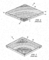
- FIGURE 4 illustrates package warpage for the semiconductor package shown in FIGURE 3 .
- FIGURE 4 illustrates only one-quarter of the package due to symmetry.
- the warpage level is highest in the region 24 near the location of the die 12 and lowest in the region 26 at a corner of the package furthest away from the die 12.
- the dotted lines 28 indicate the gradient change in warpage moving away from the center of the package toward the perimeter of the package.
- FIGURE 4 was obtained from finite element modeling, and shows the displacement contour of the package in FIGURE 3 when cooling down to room temperature for the under fill curing process.
- FIGURE 5 illustrates maximum stress in the semiconductor die 12 for the semiconductor package shown in FIGURE 3 .
- FIGURE 5 illustrates the stress contour on the die 12 obtained by finite element modeling. Only one-quarter of the die 12 was modeled due to symmetry. The maximum stress level is highest in the region 32 near the corner of the die 12 and decreases moving away from the region 34. The dotted lines 34 indicate the gradient change in maximum stress level.
- a semi-conductor package comprising: a substrate board; a semiconductor die attached to a surface of the substrate board ; and a heat spreader, attached to the top surface of the substrate board, the heat spreader including a plate portion integrally formed with a peripheral side wall portion; and a stiffener comprising a stiffening ring, with an I-shaped cross section, having a central opening sized and shaped to fit around said semiconductor die within the package, the stiffening ring consisting of a vertical leg sized and shaped to provide a space between an inner edge of the wall portion of said heat spreader and the vertical leg of the stiffening ring wherein the space permits the installation of passive electrical components.
- a semiconductor package may further comprise a supporting member, the stiffener and supporting member may comprise: a plurality of tie bars extending between and interconnecting an inner ring portion of the stiffener and an outer ring portion of said stiffener.
- the tie bars may be positioned at corners of the inner ring portion and the outer ring portion.
- the space between the inner ring portion and the outer ring portion may be sized to permit installation of passive electrical components within the package.
- the inner ring portion, outer ring portion and tie bars may be integrally formed.
- the heat spreader may be integrally formed and may have a plate portion and a peripheral sidewall portion, an edge of the peripheral sidewall portion may be attached to the surface of the substrate board; and the stiffening ring may be attached to the surface of the substrate board and may be attached to a surface of the plate portion of the heat spreader.
- the stiffener or the stiffener and supporting member may be attached to the surface of the substrate board, and the heat spreader may comprise a heat spreader plate having a surface mounted to a surface of the stiffener or the stiffener and supporting member.
- the substrate board may be an organic substrate printed wire board.
- the substrate board may have a region supporting the mounting of passive electrical components to the surface of the substrate board said region between the stiffening ring and the peripheral sidewall portion of the heat spreader or between the inner ring portion and the outer ring portion.
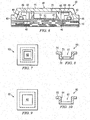
- FIGURE 6 shows a cross-sectional view of a semiconductor package.
- a semiconductor die 12 is attached to a top surface of an organic substrate printed wire board 10 using an under fill adhesive 14.
- One or more passive components 40 may also be attached to the top surface of the organic substrate printed wire board 10. Electrical connection of the die 12 to the organic substrate printed wire board 10 is made through solder bumps 42.
- a heat spreader 44 is attached to the top surface of the organic substrate printed wire board 10 using an adhesive 46 (that may, or may not, be the same as the adhesive 14).
- the heat spreader 44 includes a plate portion 48 integrally formed with a peripheral side wall portion 50. A lower edge of the peripheral side wall portion 50 is mounted to the top surface of the organic substrate printed wire board 10 with the adhesive 46.
- a thermally conductive material 20 (also known in the art as a thermal interface material), which may also comprise an adhesive, is positioned between a top surface of the die 12 and a bottom surface of the plate portion 50 for the heat spreader 44. It will be noted that the package configuration of FIGURE 6 replaces the separately provided stiffener ring 16 of FIGURE 3 at the perimeter of the package with the integrally formed side wall portion 50.
- the package of FIGURE 6 further includes a stiffening ring 60.
- This stiffening ring 60 differs from the ring 16 of FIGURE 3 in terms of both shape and position.
- the ring 60 is positioned close to the die 12 between an outer peripheral edge of the die and an inner edge of the side wall portion 50 of the heat spreader 44.
- the ring 60 is thus provided to support the bottom surface of the plate portion 48 of the heat spreader 44.
- a bottom edge of the ring is mounted to the top surface of the organic substrate printed wire board 10 with the adhesive 46.
- a top edge of the ring is mounted to the bottom surface of the plate portion 48 of the heat spreader 44 with the adhesive 46.
- the stiffening ring 60 can, in an implementation, have a cross-sectional I-shape. This implementation is not explicitly shown in FIGURE 6 , but the ring 60 in this implementation would have a cross-sectional shape similar to the ring 16 as shown in FIGURE 3 . The placement of the ring 60, however, as discussed above, would differ from the placement of the ring 16.
- a central opening 62 in the ring 60 is sized and shaped to comfortably fit the die 12 and adhesive 14.
- the outer perimeter of the ring 60 is sized and shaped to comfortably fit within the inner edge of the side wall portion 50 of the heat spreader 44.
- the stiffening ring 60 can, in an example, have a cross-sectional L-shape. This example is explicitly shown in FIGURES 6 and 10 .
- the L-shape includes a vertical leg 64 and a horizontal leg 66.
- FIGURE 9 shows a plan view of the stiffening ring 60 having a cross-sectional L-shape as shown in FIGURES 6 and 10 .
- a central opening 62 in the ring 60 is sized and shaped to comfortably fit the die 12 and adhesive 14.
- the outer perimeter of the ring 60 is sized and shaped to comfortably fit within the inner edge of the side wall portion 50 of the heat spreader 44. When installed, the cross-sectional L-shape of the stiffening ring 60 will be oriented upside-down.
- This installation orientation is advantageous in that the horizontal leg 66 provides support to the bottom surface of the plate portion 48 of the heat spreader 44 while the vertical leg 64 provides space allowing for the efficient installation of the passive components 40 (for example, surface mount components) to the top surface of the organic substrate printed wire board 10 underneath the horizontal leg 66.
- the passive components 40 for example, surface mount components
- the stiffening ring 60 can, in an example, have a cross-sectional Z-shape. This example is explicitly shown in FIGURE 8 .
- the Z-shape includes a vertical leg 70, a lower horizontal leg 72 and an upper horizontal leg 74.
- FIGURE 7 shows a plan view of the stiffening ring 60 having a cross-sectional Z-shape as shown in FIGURE 8 .
- a central opening 62 in the ring 60 is sized and shaped to comfortably fit the die 12 and adhesive 14.
- the outer perimeter of the ring 60 is sized and shaped to comfortably fit within the inner edge of the side wall portion 50 of the heat spreader 44.
- the cross-sectional Z-shape is advantageous in that the upper horizontal leg 74 provides support to the bottom surface of the plate portion 48 of the heat spreader 44 while the vertical leg 70 and lower horizontal leg 72 provide space allowing for the efficient installation of the passive components 40 (for example, surface mount components) to the top surface of the organic substrate printed wire board 10 underneath the upper horizontal leg 74.
- the passive components 40 for example, surface mount components
- the stiffening ring 60 is preferably positioned as close to the die 12 as possible. In a preferred implementation, the stiffening ring 60 is positioned between the die 12 and any included passive components 40. The stiffening ring 60 may further function as a dam for stopping the spreading of the under fill adhesive 14.
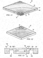
- FIGURE 11 illustrates package warpage for the semiconductor package shown in FIGURE 6 .
- finite element modeling techniques were used to obtain FIGURE 11.
- FIGURE 11 illustrates only one-quarter of the package due to symmetry of the package.
- the warpage level is highest in the region 24 near the location of the die 12 and lowest in the region 26 at a corner of the package furthest away from the die 12.
- the dotted lines 28 indicate the gradient change in warpage moving away from the center of the package toward the perimeter of the package.
- the package warpage in FIGURE 11 is 50% less than that experienced with the package of FIGURE 3 .
- FIGURE 12 illustrates maximum stress in the semiconductor die 12 for the semiconductor package shown in FIGURE 3 .
- FIGURE 12 illustrates only one-quarter of the die 12. The maximum stress level is highest in the region 32 near the corner of the die 12 and decreases moving away from the region 34. The dotted lines 34 indicate the gradient change in maximum stress level. In comparison to FIGURE 5 , the maximum stress in FIGURE 15 is 14% less than that experienced with the package of FIGURE 3 .
- Benefits of the FIGURE 6 implementation which comprises a) a single piece heat spreader; and b) an inner stiffening ring are: improved package rigidity; improved warpage and stress performance during temperature cycling; and maximizing surface area available for surface mount components on the organic substrate.
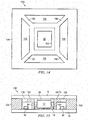
- FIGURE 13 is a cross-sectional illustration of a single piece stiffener and supporting member 100.
- a plan view of the member 100 is shown in FIGURE 14 .
- the member 100 is formed to include an inner ring structure 102 and an outer ring structure 104.
- the inner ring structure 102 has the form of the stiffening ring 60 of FIGURE 6 in the form of the I-shape.
- a central opening 62 is provided in the inner ring structure 102.
- the outer ring structure 104 has the form of the ring 16 of FIGURE 3 (for example, in the I-shape).
- Space 108 in the form of an annulus is provided between the inner ring structure 102 and the outer ring structure 104.
- the outer ring structure 104 is tied to the inner ring structure 102 by a set of tie bars 106. In a preferred implementation, the tie bars 106 are positioned at the corners of the member 100 extending from the inner ring structure 102.
- FIGURE 15 illustrates installation of the single piece stiffener and supporting member in a semiconductor package.
- a semiconductor die 12 is attached to a top surface of the organic substrate printed wire board 10 using an under fill adhesive 14.
- the single piece stiffener and supporting member 100 is attached to the top surface of the organic substrate printed wire board 10 using any suitable adhesive material.
- the inner ring structure 102 surrounds the die 12. An inner edge of the inner ring structure 102 is spaced away from an outer edge of the die 12.
- the central opening 62 provided in the inner ring structure 102 is sized and shaped to comfortably fit the die 12 and adhesive 14.
- the inner ring structure 102 may further function as a dam for stopping the spreading of the under fill adhesive 14.
- the outer ring structure 104 may, as shown, have an outer perimeter edge coincident with an outer perimeter edge of organic substrate printed wire board 10. Space 108 is provided between the inner ring structure 102 and the outer ring structure 104.
- One or more passive components 40 (for example, surface mount components) may be attached to the top surface of the organic substrate printed wire board 10 in the space 108.
- the inner ring structure 102, outer ring structure 104 and tie bars 106 are integrally formed of a same material to form the single integral piece.
- a heat spreader 18 is attached to the top surface of the single piece stiffener and supporting member 100.
- the heat spreader 18 is illustrated to be in the form of a thermally conductive plate.
- the heat spreader 18 may, as shown, have an outer perimeter edge coincident with the outer perimeter edges of the single piece stiffener and supporting member 100 and organic substrate printed wire board 10.
- the spreader 18 is attached to the single piece stiffener and supporting member 100 top surface using any suitable adhesive material.
- a thermally conductive material 20 also known in the art as a thermal interface material, which may also comprise an adhesive, is positioned between a top surface of the die 12 and a bottom surface of the heat spreader 18.
- an upper horizontal leg 66 or 74 provides support to the bottom surface of the heat spreader 18 while the vertical leg 64 or 70 provides room allowing for the efficient installation of the passive components 40 (for example, surface mount components) to the top surface of the organic substrate printed wire board 10 underneath the upper horizontal leg 66 or 74 in the space 108.
- the tie bars 106 extend from the upper horizontal leg 66 or 74 to the outer ring structure 104 in a manner which allows for the installation of the passive components 40 to the top surface of the organic substrate printed wire board 10 underneath the tie bars 106.
Landscapes
- Cooling Or The Like Of Semiconductors Or Solid State Devices (AREA)
Description
- The present invention relates generally to semiconductor packages and, more particularly, to a semiconductor package including supporting stiffening and heat spreading characteristics
- The scope of protection is defined by the claims. The figures show further examples which are not encompassed in the scope of the invention, even if they are named "embodiments" in the corresponding parts of the description.
- Reference is made to
FIGURES 1-3 which illustrate a sequence of process steps for producing a semiconductor package.FIGURE 1 shows an organic substrate printedwire board 10. Asemiconductor die 12 is attached to a top surface of the organic substrate printedwire board 10 using an under filladhesive 14.FIGURE 2 shows astiffener ring 16 that has been attached to the top surface of the organic substrate printedwire board 10. Thering 16 surrounds thedie 12 and has an outer perimeter edge coincident with an outer perimeter edge of the organic substrate printedwire board 10. An inner edge of thering 16 is spaced away from an outer edge of the die 12. Thering 12 is attached to the organic substrate printedwire board 10 top surface using any suitable adhesive material.FIGURE 3 shows aheat spreader 18 that has been attached to the top surface of thering 12. Theheat spreader 18 is illustrated to be in the form of a thermally conductive plate. Theheat spreader 18 may, as shown, have an outer perimeter edge coincident with the outer perimeter edges of thering 16 and organic substrate printedwire board 10. Thespreader 18 is attached to thering 16 top surface using any suitable adhesive material. A thermally conductive material 20 (also known in the art as a thermal interface material), which may also comprise an adhesive, is positioned between a top surface of the die 12 and a bottom surface of theheat spreader 18. - Reference is now made to
FIGURE 4 which illustrates package warpage for the semiconductor package shown inFIGURE 3 .FIGURE 4 illustrates only one-quarter of the package due to symmetry. The warpage level is highest in theregion 24 near the location of the die 12 and lowest in theregion 26 at a corner of the package furthest away from the die 12. Thedotted lines 28 indicate the gradient change in warpage moving away from the center of the package toward the perimeter of the package.FIGURE 4 was obtained from finite element modeling, and shows the displacement contour of the package inFIGURE 3 when cooling down to room temperature for the under fill curing process. - Reference is now made to
FIGURE 5 which illustrates maximum stress in thesemiconductor die 12 for the semiconductor package shown inFIGURE 3 .FIGURE 5 illustrates the stress contour on the die 12 obtained by finite element modeling. Only one-quarter of the die 12 was modeled due to symmetry. The maximum stress level is highest in theregion 32 near the corner of the die 12 and decreases moving away from theregion 34. Thedotted lines 34 indicate the gradient change in maximum stress level. - In some embodiments, there is provided a semi-conductor package comprising: a substrate board; a semiconductor die attached to a surface of the substrate board ; and a heat spreader, attached to the top surface of the substrate board, the heat spreader including a plate portion integrally formed with a peripheral side wall portion; and a stiffener comprising a stiffening ring, with an I-shaped cross section, having a central opening sized and shaped to fit around said semiconductor die within the package, the stiffening ring consisting of a vertical leg sized and shaped to provide a space between an inner edge of the wall portion of said heat spreader and the vertical leg of the stiffening ring wherein the space permits the installation of passive electrical components.
- In some embodiments, a semiconductor package may further comprise a supporting member, the stiffener and supporting member may comprise: a plurality of tie bars extending between and interconnecting an inner ring portion of the stiffener and an outer ring portion of said stiffener.
- In some embodiments, the tie bars may be positioned at corners of the inner ring portion and the outer ring portion.
- In some embodiments, the space between the inner ring portion and the outer ring portion may be sized to permit installation of passive electrical components within the package.
- In some embodiments, the inner ring portion, outer ring portion and tie bars may be integrally formed.
- In some embodiments, the heat spreader may be integrally formed and may have a plate portion and a peripheral sidewall portion, an edge of the peripheral sidewall portion may be attached to the surface of the substrate board; and the stiffening ring may be attached to the surface of the substrate board and may be attached to a surface of the plate portion of the heat spreader.
- In some embodiments, the stiffener or the stiffener and supporting member may be attached to the surface of the substrate board, and the heat spreader may comprise a heat spreader plate having a surface mounted to a surface of the stiffener or the stiffener and supporting member.
- In some embodiments, the substrate board may be an organic substrate printed wire board.
- In some embodiments, the substrate board may have a region supporting the mounting of passive electrical components to the surface of the substrate board said region between the stiffening ring and the peripheral sidewall portion of the heat spreader or between the inner ring portion and the outer ring portion.
- A more complete understanding of the method and apparatus of the present invention may be acquired by reference to the following Detailed Description when taken in conjunction with the accompanying Drawings wherein:
-
FIGURES 1-3 illustrate a sequence of process steps for producing a semiconductor package; -
FIGURE 4 illustrates package warpage for the semiconductor package shown inFIGURE 3 ; -
FIGURE 5 illustrates maximum stress in the semiconductor die for the semiconductor package shown inFIGURE 3 ; -
FIGURE 6 shows a cross-sectional view of a semiconductor package; -
FIGURES 7 and 9 show plan views of an inner stiffener ring for use in the package ofFIGURE 6 ; -
FIGURES 8 and 10 show cross-sectional views of the inner stiffener ring shown inFIGURES 7 and 9 , respectively; -
FIGURE 11 illustrates package warpage for the semiconductor package shown inFIGURE 6 ; -
FIGURE 12 illustrates maximum stress in the semiconductor die for the semiconductor package shown inFIGURE 6 ; -
FIGURE 13 is a cross-sectional illustration of a single piece stiffener and supporting member; -
FIGURE 14 is a plan view of the single piece stiffener and supporting member shown inFIGURE 13 ; and -
FIGURE 15 illustrates installation of the single piece stiffener and supporting member in a semiconductor package. - Reference is now made to
FIGURE 6 which shows a cross-sectional view of a semiconductor package. A semiconductor die 12 is attached to a top surface of an organic substrate printedwire board 10 using an underfill adhesive 14. One or more passive components 40 (for example, surface mount components) may also be attached to the top surface of the organic substrate printedwire board 10. Electrical connection of the die 12 to the organic substrate printedwire board 10 is made through solder bumps 42. Aheat spreader 44 is attached to the top surface of the organic substrate printedwire board 10 using an adhesive 46 (that may, or may not, be the same as the adhesive 14). Theheat spreader 44 includes aplate portion 48 integrally formed with a peripheralside wall portion 50. A lower edge of the peripheralside wall portion 50 is mounted to the top surface of the organic substrate printedwire board 10 with the adhesive 46. A thermally conductive material 20 (also known in the art as a thermal interface material), which may also comprise an adhesive, is positioned between a top surface of thedie 12 and a bottom surface of theplate portion 50 for theheat spreader 44. It will be noted that the package configuration ofFIGURE 6 replaces the separately providedstiffener ring 16 ofFIGURE 3 at the perimeter of the package with the integrally formedside wall portion 50. - The package of
FIGURE 6 further includes astiffening ring 60. Thisstiffening ring 60 differs from thering 16 ofFIGURE 3 in terms of both shape and position. Thering 60 is positioned close to the die 12 between an outer peripheral edge of the die and an inner edge of theside wall portion 50 of theheat spreader 44. Thering 60 is thus provided to support the bottom surface of theplate portion 48 of theheat spreader 44. A bottom edge of the ring is mounted to the top surface of the organic substrate printedwire board 10 with the adhesive 46. A top edge of the ring is mounted to the bottom surface of theplate portion 48 of theheat spreader 44 with the adhesive 46. - The stiffening
ring 60 can, in an implementation, have a cross-sectional I-shape. This implementation is not explicitly shown inFIGURE 6 , but thering 60 in this implementation would have a cross-sectional shape similar to thering 16 as shown inFIGURE 3 . The placement of thering 60, however, as discussed above, would differ from the placement of thering 16. Acentral opening 62 in thering 60 is sized and shaped to comfortably fit the die 12 and adhesive 14. The outer perimeter of thering 60 is sized and shaped to comfortably fit within the inner edge of theside wall portion 50 of theheat spreader 44. - The stiffening
ring 60 can, in an example, have a cross-sectional L-shape. This example is explicitly shown inFIGURES 6 and 10 . The L-shape includes avertical leg 64 and ahorizontal leg 66.FIGURE 9 shows a plan view of thestiffening ring 60 having a cross-sectional L-shape as shown inFIGURES 6 and 10 . Acentral opening 62 in thering 60 is sized and shaped to comfortably fit thedie 12 and adhesive 14. The outer perimeter of thering 60 is sized and shaped to comfortably fit within the inner edge of theside wall portion 50 of theheat spreader 44. When installed, the cross-sectional L-shape of thestiffening ring 60 will be oriented upside-down. This installation orientation is advantageous in that thehorizontal leg 66 provides support to the bottom surface of theplate portion 48 of theheat spreader 44 while thevertical leg 64 provides space allowing for the efficient installation of the passive components 40 (for example, surface mount components) to the top surface of the organic substrate printedwire board 10 underneath thehorizontal leg 66. - The stiffening
ring 60 can, in an example, have a cross-sectional Z-shape. This example is explicitly shown inFIGURE 8 . The Z-shape includes avertical leg 70, a lower horizontal leg 72 and an upperhorizontal leg 74.FIGURE 7 shows a plan view of thestiffening ring 60 having a cross-sectional Z-shape as shown inFIGURE 8 . Acentral opening 62 in thering 60 is sized and shaped to comfortably fit thedie 12 and adhesive 14. The outer perimeter of thering 60 is sized and shaped to comfortably fit within the inner edge of theside wall portion 50 of theheat spreader 44. The cross-sectional Z-shape is advantageous in that the upperhorizontal leg 74 provides support to the bottom surface of theplate portion 48 of theheat spreader 44 while thevertical leg 70 and lower horizontal leg 72 provide space allowing for the efficient installation of the passive components 40 (for example, surface mount components) to the top surface of the organic substrate printedwire board 10 underneath the upperhorizontal leg 74. - The stiffening
ring 60 is preferably positioned as close to the die 12 as possible. In a preferred implementation, the stiffeningring 60 is positioned between the die 12 and any includedpassive components 40. The stiffeningring 60 may further function as a dam for stopping the spreading of theunder fill adhesive 14. - Reference is now made to
FIGURE 11 which illustrates package warpage for the semiconductor package shown inFIGURE 6 . Again, finite element modeling techniques were used to obtainFIGURE 11. FIGURE 11 illustrates only one-quarter of the package due to symmetry of the package. The warpage level is highest in theregion 24 near the location of thedie 12 and lowest in theregion 26 at a corner of the package furthest away from thedie 12. The dottedlines 28 indicate the gradient change in warpage moving away from the center of the package toward the perimeter of the package. In comparison toFIGURE 4 , the package warpage inFIGURE 11 is 50% less than that experienced with the package ofFIGURE 3 . - Reference is now made to
FIGURE 12 which illustrates maximum stress in the semiconductor die 12 for the semiconductor package shown inFIGURE 3 .FIGURE 12 illustrates only one-quarter of thedie 12. The maximum stress level is highest in theregion 32 near the corner of thedie 12 and decreases moving away from theregion 34. The dottedlines 34 indicate the gradient change in maximum stress level. In comparison toFIGURE 5 , the maximum stress inFIGURE 15 is 14% less than that experienced with the package ofFIGURE 3 . - Benefits of the
FIGURE 6 implementation which comprises a) a single piece heat spreader; and b) an inner stiffening ring are: improved package rigidity; improved warpage and stress performance during temperature cycling; and maximizing surface area available for surface mount components on the organic substrate. - Reference is now made to
FIGURE 13 which is a cross-sectional illustration of a single piece stiffener and supportingmember 100. A plan view of themember 100 is shown inFIGURE 14 . Themember 100 is formed to include aninner ring structure 102 and anouter ring structure 104. Theinner ring structure 102 has the form of thestiffening ring 60 ofFIGURE 6 in the form of the I-shape. Acentral opening 62 is provided in theinner ring structure 102. Theouter ring structure 104 has the form of thering 16 ofFIGURE 3 (for example, in the I-shape).Space 108 in the form of an annulus is provided between theinner ring structure 102 and theouter ring structure 104. Theouter ring structure 104 is tied to theinner ring structure 102 by a set of tie bars 106. In a preferred implementation, the tie bars 106 are positioned at the corners of themember 100 extending from theinner ring structure 102. - Reference is now made to
FIGURE 15 which illustrates installation of the single piece stiffener and supporting member in a semiconductor package. A semiconductor die 12 is attached to a top surface of the organic substrate printedwire board 10 using an underfill adhesive 14. The single piece stiffener and supportingmember 100 is attached to the top surface of the organic substrate printedwire board 10 using any suitable adhesive material. Theinner ring structure 102 surrounds thedie 12. An inner edge of theinner ring structure 102 is spaced away from an outer edge of thedie 12. Thecentral opening 62 provided in theinner ring structure 102 is sized and shaped to comfortably fit thedie 12 and adhesive 14. Theinner ring structure 102 may further function as a dam for stopping the spreading of theunder fill adhesive 14. - The
outer ring structure 104 may, as shown, have an outer perimeter edge coincident with an outer perimeter edge of organic substrate printedwire board 10.Space 108 is provided between theinner ring structure 102 and theouter ring structure 104. One or more passive components 40 (for example, surface mount components) may be attached to the top surface of the organic substrate printedwire board 10 in thespace 108. Theinner ring structure 102,outer ring structure 104 and tiebars 106 are integrally formed of a same material to form the single integral piece. - A
heat spreader 18 is attached to the top surface of the single piece stiffener and supportingmember 100. Theheat spreader 18 is illustrated to be in the form of a thermally conductive plate. Theheat spreader 18 may, as shown, have an outer perimeter edge coincident with the outer perimeter edges of the single piece stiffener and supportingmember 100 and organic substrate printedwire board 10. Thespreader 18 is attached to the single piece stiffener and supportingmember 100 top surface using any suitable adhesive material. A thermally conductive material 20 (also known in the art as a thermal interface material), which may also comprise an adhesive, is positioned between a top surface of thedie 12 and a bottom surface of theheat spreader 18. - In some examples, an upper
horizontal leg heat spreader 18 while thevertical leg wire board 10 underneath the upperhorizontal leg space 108. The tie bars 106 extend from the upperhorizontal leg outer ring structure 104 in a manner which allows for the installation of thepassive components 40 to the top surface of the organic substrate printedwire board 10 underneath the tie bars 106.
Claims (10)
- A semi-conductor package comprising:a substrate board (10);a semiconductor die (12) attached to a surface of the substrate board (10);a heat spreader (18), attached to the top surface of the substrate board, the heat spreader including a plate portion integrally formed with a peripheral side wall portion; anda stiffener comprising a stiffening ring (60), with an I-shaped cross section, having a central opening (62) sized and shaped to fit around said semiconductor die (12) within the package (50), the stiffening ring consisting of a vertical leg sized and shaped to provide a space between an inner edge of the peripheral side wall portion of said heat spreader (18) and the vertical leg of the stiffening ring (60) wherein the space permits the installation of passive electrical components.
- A semiconductor package as claimed in claim 1, further comprising a supporting member, the stiffener and supporting member comprising:
a plurality of tie bars (106) extending between and interconnecting an inner ring portion (102) of the stiffener and an outer ring portion (104) of said stiffener. - A semiconductor package as claimed in claim 2, wherein the plurality of tie bars (106) are positioned at corners of the inner ring portion (102) and the outer ring portion (104).
- A semiconductor package as claimed in claim 2 or 3, wherein the space between the inner ring portion (102) and the outer ring portion (104) is sized to permit installation of passive electrical components within the package.
- A semiconductor package as claimed in any of claims 2 to 4, wherein the inner ring portion (102), outer ring portion (104) and tie bars (106) are integrally formed.
- A semiconductor package as claimed in any preceding claim, wherein said heat spreader (18) is integrally formed and has the plate portion and the peripheral sidewall portion, an edge of the peripheral sidewall portion being attached to the surface of the substrate board (10); and the stiffening ring (60) is attached to the surface of the substrate board (10) and attached to a surface of the plate portion of the heat spreader (18).
- A semiconductor package as claimed in any of claims 2 to 5, wherein the stiffener or the stiffener and supporting member (100) is attached to the surface of the substrate board (10), and the heat spreader (18) comprises a heat spreader plate having a surface mounted to a surface of the stiffener or the stiffener and supporting member (100).
- A package as claimed in claims 6 or 7, comprising a thermal interface material positioned between a surface of the semiconductor die (12) and the surface of the plate or plate portion of the heat spreader (18).
- A package as claimed in claims 5, 6 or 7, wherein the substrate board (10) is an organic substrate printed wire board.
- A package as claimed in claim 6 or 7, or any claim appended thereto, wherein the substrate board (10) has a region supporting the mounting of passive electrical components to the surface of the substrate board (10) said region between the stiffening ring (60) and the peripheral sidewall portion of the heat spreader (18) or between the inner ring portion (102) and the outer ring portion (104).
Applications Claiming Priority (2)
| Application Number | Priority Date | Filing Date | Title |
|---|---|---|---|
| US12/507,049 US8013438B2 (en) | 2009-07-21 | 2009-07-21 | Semiconductor package with a stiffening member supporting a thermal heat spreader |
| EP10170318.9A EP2278615B1 (en) | 2009-07-21 | 2010-07-21 | Semiconductor package with a stiffening member supporting a thermal heat spreader |
Related Parent Applications (2)
| Application Number | Title | Priority Date | Filing Date |
|---|---|---|---|
| EP10170318.9A Division EP2278615B1 (en) | 2009-07-21 | 2010-07-21 | Semiconductor package with a stiffening member supporting a thermal heat spreader |
| EP10170318.9A Division-Into EP2278615B1 (en) | 2009-07-21 | 2010-07-21 | Semiconductor package with a stiffening member supporting a thermal heat spreader |
Publications (2)
| Publication Number | Publication Date |
|---|---|
| EP3349245A1 EP3349245A1 (en) | 2018-07-18 |
| EP3349245B1 true EP3349245B1 (en) | 2021-03-24 |
Family
ID=42985658
Family Applications (2)
| Application Number | Title | Priority Date | Filing Date |
|---|---|---|---|
| EP18159488.8A Active EP3349245B1 (en) | 2009-07-21 | 2010-07-21 | Semiconductor package with a stiffening member supporting a thermal heat spreader |
| EP10170318.9A Active EP2278615B1 (en) | 2009-07-21 | 2010-07-21 | Semiconductor package with a stiffening member supporting a thermal heat spreader |
Family Applications After (1)
| Application Number | Title | Priority Date | Filing Date |
|---|---|---|---|
| EP10170318.9A Active EP2278615B1 (en) | 2009-07-21 | 2010-07-21 | Semiconductor package with a stiffening member supporting a thermal heat spreader |
Country Status (2)
| Country | Link |
|---|---|
| US (1) | US8013438B2 (en) |
| EP (2) | EP3349245B1 (en) |
Families Citing this family (29)
| Publication number | Priority date | Publication date | Assignee | Title |
|---|---|---|---|---|
| US8390112B2 (en) * | 2008-09-30 | 2013-03-05 | Intel Corporation | Underfill process and materials for singulated heat spreader stiffener for thin core panel processing |
| US9202769B2 (en) * | 2009-11-25 | 2015-12-01 | Stats Chippac, Ltd. | Semiconductor device and method of forming thermal lid for balancing warpage and thermal management |
| US8034661B2 (en) | 2009-11-25 | 2011-10-11 | Stats Chippac, Ltd. | Semiconductor device and method of forming compliant stress relief buffer around large array WLCSP |
| US10115654B2 (en) * | 2010-06-18 | 2018-10-30 | Palo Alto Research Center Incorporated | Buried thermally conductive layers for heat extraction and shielding |
| US8976529B2 (en) * | 2011-01-14 | 2015-03-10 | Taiwan Semiconductor Manufacturing Company, Ltd. | Lid design for reliability enhancement in flip chip package |
| KR20140115668A (en) | 2013-03-21 | 2014-10-01 | 삼성전자주식회사 | Semiconductor package having a heat slug and a passive device |
| US9076754B2 (en) | 2013-08-02 | 2015-07-07 | Taiwan Semiconductor Manufacturing Company, Ltd. | 3DIC packages with heat sinks attached to heat dissipating rings |
| US9082743B2 (en) | 2013-08-02 | 2015-07-14 | Taiwan Semiconductor Manufacturing Company, Ltd. | 3DIC packages with heat dissipation structures |
| US9583415B2 (en) * | 2013-08-02 | 2017-02-28 | Taiwan Semiconductor Manufacturing Company, Ltd. | Packages with thermal interface material on the sidewalls of stacked dies |
| US9275876B2 (en) * | 2013-09-30 | 2016-03-01 | Qualcomm Incorporated | Stiffener with embedded passive components |
| JP6421050B2 (en) * | 2015-02-09 | 2018-11-07 | 株式会社ジェイデバイス | Semiconductor device |
| US9570373B1 (en) * | 2015-12-09 | 2017-02-14 | International Business Machines Corporation | Near-chip compliant layer for reducing perimeter stress during assembly process |
| US9799610B2 (en) * | 2015-12-18 | 2017-10-24 | Intel Corporation | Plurality of stiffeners with thickness variation |
| US10157860B2 (en) * | 2016-12-28 | 2018-12-18 | Intel Corporation | Component stiffener architectures for microelectronic package structures |
| US11676873B2 (en) * | 2017-06-30 | 2023-06-13 | Intel Corporation | Semiconductor package having sealant bridge |
| US10957611B2 (en) * | 2017-08-01 | 2021-03-23 | Mediatek Inc. | Semiconductor package including lid structure with opening and recess |
| US11076510B2 (en) * | 2018-08-13 | 2021-07-27 | Facebook Technologies, Llc | Heat management device and method of manufacture |
| CN109755197A (en) * | 2019-01-14 | 2019-05-14 | 苏州通富超威半导体有限公司 | Encapsulating structure and forming method thereof |
| CN110416097B (en) * | 2019-06-12 | 2021-05-11 | 苏州通富超威半导体有限公司 | Packaging structure and packaging method for preventing indium metal from overflowing |
| US11948855B1 (en) | 2019-09-27 | 2024-04-02 | Rockwell Collins, Inc. | Integrated circuit (IC) package with cantilever multi-chip module (MCM) heat spreader |
| CN111403349A (en) * | 2020-03-04 | 2020-07-10 | 苏州通富超威半导体有限公司 | Passive element protection structure and chip packaging assembly |
| US11721602B2 (en) * | 2021-05-06 | 2023-08-08 | Taiwan Semiconductor Manufacturing Company, Ltd. | Semiconductor package with stiffener structure |
| US11929293B2 (en) * | 2021-08-19 | 2024-03-12 | Taiwan Semiconductor Manufacturing Company, Ltd. | Semiconductor package with lid structure |
| KR20230100054A (en) * | 2021-12-28 | 2023-07-05 | 삼성전자주식회사 | Semiconductor package including stiffener |
| US20240071857A1 (en) * | 2022-08-31 | 2024-02-29 | Taiwan Semiconductor Manufacturing Company, Ltd. | Semiconductor device |
| US12532741B2 (en) * | 2022-11-11 | 2026-01-20 | Amkor Technology Singapore Holding Pte. Ltd. | Semiconductor devices and methods of manufacturing semiconductor devices |
| US20250006572A1 (en) * | 2023-06-29 | 2025-01-02 | Taiwan Semiconductor Manufacturing Company Limited | Package structure including ring structure and methods of forming the same |
| US20250046674A1 (en) * | 2023-08-03 | 2025-02-06 | Apple Inc. | Recess Island Lid Design for TIM Delamination Risk Mitigation |
| US20250079246A1 (en) * | 2023-09-05 | 2025-03-06 | Taiwan Semiconductor Manufacturing Company, Ltd. | Semiconductor package with stiffener structure |
Family Cites Families (12)
| Publication number | Priority date | Publication date | Assignee | Title |
|---|---|---|---|---|
| JPH0786471A (en) * | 1993-09-20 | 1995-03-31 | Hitachi Ltd | Semiconductor module |
| US5923538A (en) * | 1994-10-17 | 1999-07-13 | Lsi Logic Corporation | Support member for mounting a microelectronic circuit package |
| EP0742682B1 (en) * | 1995-05-12 | 2005-02-23 | STMicroelectronics, Inc. | Low-profile socketed integrated circuit packaging system |
| US6011304A (en) * | 1997-05-05 | 2000-01-04 | Lsi Logic Corporation | Stiffener ring attachment with holes and removable snap-in heat sink or heat spreader/lid |
| US6008536A (en) * | 1997-06-23 | 1999-12-28 | Lsi Logic Corporation | Grid array device package including advanced heat transfer mechanisms |
| US6552267B2 (en) * | 2001-08-13 | 2003-04-22 | Taiwan Semiconductor Manufacturing Co., Ltd. | Microelectronic assembly with stiffening member |
| US6876553B2 (en) * | 2002-03-21 | 2005-04-05 | Broadcom Corporation | Enhanced die-up ball grid array package with two substrates |
| US7482686B2 (en) * | 2004-06-21 | 2009-01-27 | Braodcom Corporation | Multipiece apparatus for thermal and electromagnetic interference (EMI) shielding enhancement in die-up array packages and method of making the same |
| US7449775B1 (en) * | 2006-05-22 | 2008-11-11 | Sun Microsystems, Inc. | Integrated thermal solution for electronic packages with materials having mismatched coefficient of thermal expansion |
| US20080099910A1 (en) * | 2006-08-31 | 2008-05-01 | Ati Technologies Inc. | Flip-Chip Semiconductor Package with Encapsulant Retaining Structure and Strip |
| KR100802393B1 (en) * | 2007-02-15 | 2008-02-13 | 삼성전기주식회사 | Package board and its manufacturing method |
| US20080284047A1 (en) * | 2007-05-15 | 2008-11-20 | Eric Tosaya | Chip Package with Stiffener Ring |
-
2009
- 2009-07-21 US US12/507,049 patent/US8013438B2/en active Active
-
2010
- 2010-07-21 EP EP18159488.8A patent/EP3349245B1/en active Active
- 2010-07-21 EP EP10170318.9A patent/EP2278615B1/en active Active
Non-Patent Citations (1)
| Title |
|---|
| None * |
Also Published As
| Publication number | Publication date |
|---|---|
| EP2278615A2 (en) | 2011-01-26 |
| US20110018125A1 (en) | 2011-01-27 |
| EP3349245A1 (en) | 2018-07-18 |
| EP2278615B1 (en) | 2018-04-18 |
| US8013438B2 (en) | 2011-09-06 |
| EP2278615A3 (en) | 2011-06-15 |
Similar Documents
| Publication | Publication Date | Title |
|---|---|---|
| US8013438B2 (en) | Semiconductor package with a stiffening member supporting a thermal heat spreader | |
| KR101919248B1 (en) | Semiconductor device package with warpage control structure | |
| EP2487710B1 (en) | Semiconductor device manufacturing method | |
| EP2311084B1 (en) | Flip chip overmold package | |
| US20140167243A1 (en) | Semiconductor packages using a chip constraint means | |
| US9287194B2 (en) | Packaging devices and methods for semiconductor devices | |
| US9041192B2 (en) | Hybrid thermal interface material for IC packages with integrated heat spreader | |
| US20090127700A1 (en) | Thermal conductor lids for area array packaged multi-chip modules and methods to dissipate heat from multi-chip modules | |
| US10840165B2 (en) | Electronics package with improved thermal performance | |
| US8207620B2 (en) | Flip-chip semiconductor package and chip carrier for preventing corner delamination | |
| JP2013513942A5 (en) | ||
| US9142523B2 (en) | Semiconductor device and manufacturing method thereof | |
| EP3792969B1 (en) | Semiconductor package having liquid-cooling lid | |
| US11587887B2 (en) | Semiconductor device and manufacturing method thereof | |
| CN113380725A (en) | Chip packaging structure and packaging method | |
| US20030089976A1 (en) | Heat sink with collapse structure and semiconductor package with heat sink | |
| US7485496B2 (en) | Semiconductor device package with a heat sink and method for fabricating the same | |
| US10964627B2 (en) | Integrated electronic device having a dissipative package, in particular dual side cooling package | |
| US7863730B2 (en) | Array-molded package heat spreader and fabrication method therefor | |
| TW201448128A (en) | Semiconductor package structure | |
| CN104282635B (en) | Semiconductor module with interlocking connection | |
| US8786075B1 (en) | Electrical circuit with component-accommodating lid | |
| US20070262444A1 (en) | Semiconductor device and chip structure thereof | |
| KR100940760B1 (en) | Semiconductor package | |
| US11948855B1 (en) | Integrated circuit (IC) package with cantilever multi-chip module (MCM) heat spreader |
Legal Events
| Date | Code | Title | Description |
|---|---|---|---|
| PUAI | Public reference made under article 153(3) epc to a published international application that has entered the european phase |
Free format text: ORIGINAL CODE: 0009012 |
|
| STAA | Information on the status of an ep patent application or granted ep patent |
Free format text: STATUS: THE APPLICATION HAS BEEN PUBLISHED |
|
| AC | Divisional application: reference to earlier application |
Ref document number: 2278615 Country of ref document: EP Kind code of ref document: P |
|
| AK | Designated contracting states |
Kind code of ref document: A1 Designated state(s): AL AT BE BG CH CY CZ DE DK EE ES FI FR GB GR HR HU IE IS IT LI LT LU LV MC MK MT NL NO PL PT RO SE SI SK SM TR |
|
| STAA | Information on the status of an ep patent application or granted ep patent |
Free format text: STATUS: REQUEST FOR EXAMINATION WAS MADE |
|
| 17P | Request for examination filed |
Effective date: 20190109 |
|
| RBV | Designated contracting states (corrected) |
Designated state(s): AL AT BE BG CH CY CZ DE DK EE ES FI FR GB GR HR HU IE IS IT LI LT LU LV MC MK MT NL NO PL PT RO SE SI SK SM TR |
|
| STAA | Information on the status of an ep patent application or granted ep patent |
Free format text: STATUS: EXAMINATION IS IN PROGRESS |
|
| 17Q | First examination report despatched |
Effective date: 20190305 |
|
| GRAP | Despatch of communication of intention to grant a patent |
Free format text: ORIGINAL CODE: EPIDOSNIGR1 |
|
| STAA | Information on the status of an ep patent application or granted ep patent |
Free format text: STATUS: GRANT OF PATENT IS INTENDED |
|
| INTG | Intention to grant announced |
Effective date: 20200512 |
|
| GRAJ | Information related to disapproval of communication of intention to grant by the applicant or resumption of examination proceedings by the epo deleted |
Free format text: ORIGINAL CODE: EPIDOSDIGR1 |
|
| STAA | Information on the status of an ep patent application or granted ep patent |
Free format text: STATUS: EXAMINATION IS IN PROGRESS |
|
| GRAS | Grant fee paid |
Free format text: ORIGINAL CODE: EPIDOSNIGR3 |
|
| STAA | Information on the status of an ep patent application or granted ep patent |
Free format text: STATUS: GRANT OF PATENT IS INTENDED |
|
| GRAP | Despatch of communication of intention to grant a patent |
Free format text: ORIGINAL CODE: EPIDOSNIGR1 |
|
| INTC | Intention to grant announced (deleted) | ||
| INTG | Intention to grant announced |
Effective date: 20201007 |
|
| GRAA | (expected) grant |
Free format text: ORIGINAL CODE: 0009210 |
|
| STAA | Information on the status of an ep patent application or granted ep patent |
Free format text: STATUS: THE PATENT HAS BEEN GRANTED |
|
| AC | Divisional application: reference to earlier application |
Ref document number: 2278615 Country of ref document: EP Kind code of ref document: P |
|
| AK | Designated contracting states |
Kind code of ref document: B1 Designated state(s): AL AT BE BG CH CY CZ DE DK EE ES FI FR GB GR HR HU IE IS IT LI LT LU LV MC MK MT NL NO PL PT RO SE SI SK SM TR |
|
| REG | Reference to a national code |
Ref country code: GB Ref legal event code: FG4D |
|
| REG | Reference to a national code |
Ref country code: CH Ref legal event code: EP |
|
| REG | Reference to a national code |
Ref country code: DE Ref legal event code: R096 Ref document number: 602010066669 Country of ref document: DE |
|
| REG | Reference to a national code |
Ref country code: IE Ref legal event code: FG4D |
|
| REG | Reference to a national code |
Ref country code: AT Ref legal event code: REF Ref document number: 1375356 Country of ref document: AT Kind code of ref document: T Effective date: 20210415 |
|
| REG | Reference to a national code |
Ref country code: LT Ref legal event code: MG9D |
|
| PG25 | Lapsed in a contracting state [announced via postgrant information from national office to epo] |
Ref country code: NO Free format text: LAPSE BECAUSE OF FAILURE TO SUBMIT A TRANSLATION OF THE DESCRIPTION OR TO PAY THE FEE WITHIN THE PRESCRIBED TIME-LIMIT Effective date: 20210624 Ref country code: GR Free format text: LAPSE BECAUSE OF FAILURE TO SUBMIT A TRANSLATION OF THE DESCRIPTION OR TO PAY THE FEE WITHIN THE PRESCRIBED TIME-LIMIT Effective date: 20210625 Ref country code: HR Free format text: LAPSE BECAUSE OF FAILURE TO SUBMIT A TRANSLATION OF THE DESCRIPTION OR TO PAY THE FEE WITHIN THE PRESCRIBED TIME-LIMIT Effective date: 20210324 Ref country code: FI Free format text: LAPSE BECAUSE OF FAILURE TO SUBMIT A TRANSLATION OF THE DESCRIPTION OR TO PAY THE FEE WITHIN THE PRESCRIBED TIME-LIMIT Effective date: 20210324 Ref country code: BG Free format text: LAPSE BECAUSE OF FAILURE TO SUBMIT A TRANSLATION OF THE DESCRIPTION OR TO PAY THE FEE WITHIN THE PRESCRIBED TIME-LIMIT Effective date: 20210624 |
|
| PG25 | Lapsed in a contracting state [announced via postgrant information from national office to epo] |
Ref country code: LV Free format text: LAPSE BECAUSE OF FAILURE TO SUBMIT A TRANSLATION OF THE DESCRIPTION OR TO PAY THE FEE WITHIN THE PRESCRIBED TIME-LIMIT Effective date: 20210324 Ref country code: SE Free format text: LAPSE BECAUSE OF FAILURE TO SUBMIT A TRANSLATION OF THE DESCRIPTION OR TO PAY THE FEE WITHIN THE PRESCRIBED TIME-LIMIT Effective date: 20210324 |
|
| REG | Reference to a national code |
Ref country code: NL Ref legal event code: MP Effective date: 20210324 |
|
| REG | Reference to a national code |
Ref country code: AT Ref legal event code: MK05 Ref document number: 1375356 Country of ref document: AT Kind code of ref document: T Effective date: 20210324 |
|
| PG25 | Lapsed in a contracting state [announced via postgrant information from national office to epo] |
Ref country code: NL Free format text: LAPSE BECAUSE OF FAILURE TO SUBMIT A TRANSLATION OF THE DESCRIPTION OR TO PAY THE FEE WITHIN THE PRESCRIBED TIME-LIMIT Effective date: 20210324 |
|
| PG25 | Lapsed in a contracting state [announced via postgrant information from national office to epo] |
Ref country code: AT Free format text: LAPSE BECAUSE OF FAILURE TO SUBMIT A TRANSLATION OF THE DESCRIPTION OR TO PAY THE FEE WITHIN THE PRESCRIBED TIME-LIMIT Effective date: 20210324 Ref country code: SM Free format text: LAPSE BECAUSE OF FAILURE TO SUBMIT A TRANSLATION OF THE DESCRIPTION OR TO PAY THE FEE WITHIN THE PRESCRIBED TIME-LIMIT Effective date: 20210324 Ref country code: EE Free format text: LAPSE BECAUSE OF FAILURE TO SUBMIT A TRANSLATION OF THE DESCRIPTION OR TO PAY THE FEE WITHIN THE PRESCRIBED TIME-LIMIT Effective date: 20210324 Ref country code: CZ Free format text: LAPSE BECAUSE OF FAILURE TO SUBMIT A TRANSLATION OF THE DESCRIPTION OR TO PAY THE FEE WITHIN THE PRESCRIBED TIME-LIMIT Effective date: 20210324 Ref country code: LT Free format text: LAPSE BECAUSE OF FAILURE TO SUBMIT A TRANSLATION OF THE DESCRIPTION OR TO PAY THE FEE WITHIN THE PRESCRIBED TIME-LIMIT Effective date: 20210324 |
|
| PG25 | Lapsed in a contracting state [announced via postgrant information from national office to epo] |
Ref country code: IS Free format text: LAPSE BECAUSE OF FAILURE TO SUBMIT A TRANSLATION OF THE DESCRIPTION OR TO PAY THE FEE WITHIN THE PRESCRIBED TIME-LIMIT Effective date: 20210724 Ref country code: PT Free format text: LAPSE BECAUSE OF FAILURE TO SUBMIT A TRANSLATION OF THE DESCRIPTION OR TO PAY THE FEE WITHIN THE PRESCRIBED TIME-LIMIT Effective date: 20210726 Ref country code: PL Free format text: LAPSE BECAUSE OF FAILURE TO SUBMIT A TRANSLATION OF THE DESCRIPTION OR TO PAY THE FEE WITHIN THE PRESCRIBED TIME-LIMIT Effective date: 20210324 Ref country code: RO Free format text: LAPSE BECAUSE OF FAILURE TO SUBMIT A TRANSLATION OF THE DESCRIPTION OR TO PAY THE FEE WITHIN THE PRESCRIBED TIME-LIMIT Effective date: 20210324 Ref country code: SK Free format text: LAPSE BECAUSE OF FAILURE TO SUBMIT A TRANSLATION OF THE DESCRIPTION OR TO PAY THE FEE WITHIN THE PRESCRIBED TIME-LIMIT Effective date: 20210324 |
|
| REG | Reference to a national code |
Ref country code: DE Ref legal event code: R097 Ref document number: 602010066669 Country of ref document: DE |
|
| PG25 | Lapsed in a contracting state [announced via postgrant information from national office to epo] |
Ref country code: ES Free format text: LAPSE BECAUSE OF FAILURE TO SUBMIT A TRANSLATION OF THE DESCRIPTION OR TO PAY THE FEE WITHIN THE PRESCRIBED TIME-LIMIT Effective date: 20210324 Ref country code: AL Free format text: LAPSE BECAUSE OF FAILURE TO SUBMIT A TRANSLATION OF THE DESCRIPTION OR TO PAY THE FEE WITHIN THE PRESCRIBED TIME-LIMIT Effective date: 20210324 Ref country code: DK Free format text: LAPSE BECAUSE OF FAILURE TO SUBMIT A TRANSLATION OF THE DESCRIPTION OR TO PAY THE FEE WITHIN THE PRESCRIBED TIME-LIMIT Effective date: 20210324 |
|
| PLBE | No opposition filed within time limit |
Free format text: ORIGINAL CODE: 0009261 |
|
| STAA | Information on the status of an ep patent application or granted ep patent |
Free format text: STATUS: NO OPPOSITION FILED WITHIN TIME LIMIT |
|
| PG25 | Lapsed in a contracting state [announced via postgrant information from national office to epo] |
Ref country code: SI Free format text: LAPSE BECAUSE OF FAILURE TO SUBMIT A TRANSLATION OF THE DESCRIPTION OR TO PAY THE FEE WITHIN THE PRESCRIBED TIME-LIMIT Effective date: 20210324 |
|
| REG | Reference to a national code |
Ref country code: CH Ref legal event code: PL |
|
| 26N | No opposition filed |
Effective date: 20220104 |
|
| GBPC | Gb: european patent ceased through non-payment of renewal fee |
Effective date: 20210721 |
|
| PG25 | Lapsed in a contracting state [announced via postgrant information from national office to epo] |
Ref country code: MC Free format text: LAPSE BECAUSE OF FAILURE TO SUBMIT A TRANSLATION OF THE DESCRIPTION OR TO PAY THE FEE WITHIN THE PRESCRIBED TIME-LIMIT Effective date: 20210324 |
|
| REG | Reference to a national code |
Ref country code: BE Ref legal event code: MM Effective date: 20210731 |
|
| PG25 | Lapsed in a contracting state [announced via postgrant information from national office to epo] |
Ref country code: LI Free format text: LAPSE BECAUSE OF NON-PAYMENT OF DUE FEES Effective date: 20210731 Ref country code: GB Free format text: LAPSE BECAUSE OF NON-PAYMENT OF DUE FEES Effective date: 20210721 Ref country code: CH Free format text: LAPSE BECAUSE OF NON-PAYMENT OF DUE FEES Effective date: 20210731 |
|
| PG25 | Lapsed in a contracting state [announced via postgrant information from national office to epo] |
Ref country code: IS Free format text: LAPSE BECAUSE OF FAILURE TO SUBMIT A TRANSLATION OF THE DESCRIPTION OR TO PAY THE FEE WITHIN THE PRESCRIBED TIME-LIMIT Effective date: 20210724 Ref country code: LU Free format text: LAPSE BECAUSE OF NON-PAYMENT OF DUE FEES Effective date: 20210721 Ref country code: FR Free format text: LAPSE BECAUSE OF NON-PAYMENT OF DUE FEES Effective date: 20210731 |
|
| PG25 | Lapsed in a contracting state [announced via postgrant information from national office to epo] |
Ref country code: IE Free format text: LAPSE BECAUSE OF NON-PAYMENT OF DUE FEES Effective date: 20210721 Ref country code: BE Free format text: LAPSE BECAUSE OF NON-PAYMENT OF DUE FEES Effective date: 20210731 |
|
| PG25 | Lapsed in a contracting state [announced via postgrant information from national office to epo] |
Ref country code: IT Free format text: LAPSE BECAUSE OF FAILURE TO SUBMIT A TRANSLATION OF THE DESCRIPTION OR TO PAY THE FEE WITHIN THE PRESCRIBED TIME-LIMIT Effective date: 20210324 |
|
| PG25 | Lapsed in a contracting state [announced via postgrant information from national office to epo] |
Ref country code: HU Free format text: LAPSE BECAUSE OF FAILURE TO SUBMIT A TRANSLATION OF THE DESCRIPTION OR TO PAY THE FEE WITHIN THE PRESCRIBED TIME-LIMIT; INVALID AB INITIO Effective date: 20100721 Ref country code: CY Free format text: LAPSE BECAUSE OF FAILURE TO SUBMIT A TRANSLATION OF THE DESCRIPTION OR TO PAY THE FEE WITHIN THE PRESCRIBED TIME-LIMIT Effective date: 20210324 |
|
| PG25 | Lapsed in a contracting state [announced via postgrant information from national office to epo] |
Ref country code: MK Free format text: LAPSE BECAUSE OF FAILURE TO SUBMIT A TRANSLATION OF THE DESCRIPTION OR TO PAY THE FEE WITHIN THE PRESCRIBED TIME-LIMIT Effective date: 20210324 |
|
| PG25 | Lapsed in a contracting state [announced via postgrant information from national office to epo] |
Ref country code: TR Free format text: LAPSE BECAUSE OF FAILURE TO SUBMIT A TRANSLATION OF THE DESCRIPTION OR TO PAY THE FEE WITHIN THE PRESCRIBED TIME-LIMIT Effective date: 20210324 |
|
| REG | Reference to a national code |
Ref country code: DE Ref legal event code: R081 Ref document number: 602010066669 Country of ref document: DE Owner name: STMICROELECTRONICS INTERNATIONAL N.V., PLAN-LE, CH Free format text: FORMER OWNER: STMICROELECTRONICS ASIA PACIFIC PTE LTD., SINGAPORE, SG |
|
| PG25 | Lapsed in a contracting state [announced via postgrant information from national office to epo] |
Ref country code: MT Free format text: LAPSE BECAUSE OF FAILURE TO SUBMIT A TRANSLATION OF THE DESCRIPTION OR TO PAY THE FEE WITHIN THE PRESCRIBED TIME-LIMIT Effective date: 20210324 |
|
| PGFP | Annual fee paid to national office [announced via postgrant information from national office to epo] |
Ref country code: DE Payment date: 20250620 Year of fee payment: 16 |
|
| REG | Reference to a national code |
Ref country code: DE Ref legal event code: R079 Ref document number: 602010066669 Country of ref document: DE Free format text: PREVIOUS MAIN CLASS: H01L0023160000 Ipc: H10W0076400000 |
|
| REG | Reference to a national code |
Ref country code: DE Ref legal event code: R082 Ref document number: 602010066669 Country of ref document: DE Representative=s name: WESTPHAL, MUSSGNUG & PARTNER PATENTANWAELTE MI, DE |