EP3348490A1 - Sticker having ic tag, and mounting method thereof - Google Patents
Sticker having ic tag, and mounting method thereof Download PDFInfo
- Publication number
- EP3348490A1 EP3348490A1 EP16843662.4A EP16843662A EP3348490A1 EP 3348490 A1 EP3348490 A1 EP 3348490A1 EP 16843662 A EP16843662 A EP 16843662A EP 3348490 A1 EP3348490 A1 EP 3348490A1
- Authority
- EP
- European Patent Office
- Prior art keywords
- tag
- sticker
- disconnection detection
- antenna
- recited
- Prior art date
- Legal status (The legal status is an assumption and is not a legal conclusion. Google has not performed a legal analysis and makes no representation as to the accuracy of the status listed.)
- Granted
Links
Images






Classifications
-
- G—PHYSICS
- G06—COMPUTING OR CALCULATING; COUNTING
- G06K—GRAPHICAL DATA READING; PRESENTATION OF DATA; RECORD CARRIERS; HANDLING RECORD CARRIERS
- G06K19/00—Record carriers for use with machines and with at least a part designed to carry digital markings
- G06K19/06—Record carriers for use with machines and with at least a part designed to carry digital markings characterised by the kind of the digital marking, e.g. shape, nature, code
- G06K19/067—Record carriers with conductive marks, printed circuits or semiconductor circuit elements, e.g. credit or identity cards also with resonating or responding marks without active components
- G06K19/07—Record carriers with conductive marks, printed circuits or semiconductor circuit elements, e.g. credit or identity cards also with resonating or responding marks without active components with integrated circuit chips
- G06K19/077—Constructional details, e.g. mounting of circuits in the carrier
- G06K19/07749—Constructional details, e.g. mounting of circuits in the carrier the record carrier being capable of non-contact communication, e.g. constructional details of the antenna of a non-contact smart card
- G06K19/07798—Constructional details, e.g. mounting of circuits in the carrier the record carrier being capable of non-contact communication, e.g. constructional details of the antenna of a non-contact smart card part of the antenna or the integrated circuit being adapted for rupturing or breaking, e.g. record carriers functioning as sealing devices for detecting not-authenticated opening of containers
-
- B—PERFORMING OPERATIONS; TRANSPORTING
- B65—CONVEYING; PACKING; STORING; HANDLING THIN OR FILAMENTARY MATERIAL
- B65B—MACHINES, APPARATUS OR DEVICES FOR, OR METHODS OF, PACKAGING ARTICLES OR MATERIALS; UNPACKING
- B65B57/00—Automatic control, checking, warning, or safety devices
-
- B—PERFORMING OPERATIONS; TRANSPORTING
- B65—CONVEYING; PACKING; STORING; HANDLING THIN OR FILAMENTARY MATERIAL
- B65D—CONTAINERS FOR STORAGE OR TRANSPORT OF ARTICLES OR MATERIALS, e.g. BAGS, BARRELS, BOTTLES, BOXES, CANS, CARTONS, CRATES, DRUMS, JARS, TANKS, HOPPERS, FORWARDING CONTAINERS; ACCESSORIES, CLOSURES, OR FITTINGS THEREFOR; PACKAGING ELEMENTS; PACKAGES
- B65D55/00—Accessories for container closures not otherwise provided for
- B65D55/02—Locking devices; Means for discouraging or indicating unauthorised opening or removal of closure
- B65D55/06—Deformable or tearable wires, strings or strips; Use of seals
-
- G—PHYSICS
- G06—COMPUTING OR CALCULATING; COUNTING
- G06K—GRAPHICAL DATA READING; PRESENTATION OF DATA; RECORD CARRIERS; HANDLING RECORD CARRIERS
- G06K19/00—Record carriers for use with machines and with at least a part designed to carry digital markings
- G06K19/06—Record carriers for use with machines and with at least a part designed to carry digital markings characterised by the kind of the digital marking, e.g. shape, nature, code
- G06K19/067—Record carriers with conductive marks, printed circuits or semiconductor circuit elements, e.g. credit or identity cards also with resonating or responding marks without active components
- G06K19/07—Record carriers with conductive marks, printed circuits or semiconductor circuit elements, e.g. credit or identity cards also with resonating or responding marks without active components with integrated circuit chips
- G06K19/073—Special arrangements for circuits, e.g. for protecting identification code in memory
- G06K19/07309—Means for preventing undesired reading or writing from or onto record carriers
- G06K19/07372—Means for preventing undesired reading or writing from or onto record carriers by detecting tampering with the circuit
-
- G—PHYSICS
- G06—COMPUTING OR CALCULATING; COUNTING
- G06K—GRAPHICAL DATA READING; PRESENTATION OF DATA; RECORD CARRIERS; HANDLING RECORD CARRIERS
- G06K19/00—Record carriers for use with machines and with at least a part designed to carry digital markings
- G06K19/06—Record carriers for use with machines and with at least a part designed to carry digital markings characterised by the kind of the digital marking, e.g. shape, nature, code
- G06K19/067—Record carriers with conductive marks, printed circuits or semiconductor circuit elements, e.g. credit or identity cards also with resonating or responding marks without active components
- G06K19/07—Record carriers with conductive marks, printed circuits or semiconductor circuit elements, e.g. credit or identity cards also with resonating or responding marks without active components with integrated circuit chips
- G06K19/077—Constructional details, e.g. mounting of circuits in the carrier
- G06K19/07749—Constructional details, e.g. mounting of circuits in the carrier the record carrier being capable of non-contact communication, e.g. constructional details of the antenna of a non-contact smart card
- G06K19/07758—Constructional details, e.g. mounting of circuits in the carrier the record carrier being capable of non-contact communication, e.g. constructional details of the antenna of a non-contact smart card arrangements for adhering the record carrier to further objects or living beings, functioning as an identification tag
-
- G—PHYSICS
- G06—COMPUTING OR CALCULATING; COUNTING
- G06K—GRAPHICAL DATA READING; PRESENTATION OF DATA; RECORD CARRIERS; HANDLING RECORD CARRIERS
- G06K19/00—Record carriers for use with machines and with at least a part designed to carry digital markings
- G06K19/06—Record carriers for use with machines and with at least a part designed to carry digital markings characterised by the kind of the digital marking, e.g. shape, nature, code
- G06K19/067—Record carriers with conductive marks, printed circuits or semiconductor circuit elements, e.g. credit or identity cards also with resonating or responding marks without active components
- G06K19/07—Record carriers with conductive marks, printed circuits or semiconductor circuit elements, e.g. credit or identity cards also with resonating or responding marks without active components with integrated circuit chips
- G06K19/077—Constructional details, e.g. mounting of circuits in the carrier
- G06K19/07749—Constructional details, e.g. mounting of circuits in the carrier the record carrier being capable of non-contact communication, e.g. constructional details of the antenna of a non-contact smart card
- G06K19/07758—Constructional details, e.g. mounting of circuits in the carrier the record carrier being capable of non-contact communication, e.g. constructional details of the antenna of a non-contact smart card arrangements for adhering the record carrier to further objects or living beings, functioning as an identification tag
- G06K19/0776—Constructional details, e.g. mounting of circuits in the carrier the record carrier being capable of non-contact communication, e.g. constructional details of the antenna of a non-contact smart card arrangements for adhering the record carrier to further objects or living beings, functioning as an identification tag the adhering arrangement being a layer of adhesive, so that the record carrier can function as a sticker
-
- G—PHYSICS
- G06—COMPUTING OR CALCULATING; COUNTING
- G06K—GRAPHICAL DATA READING; PRESENTATION OF DATA; RECORD CARRIERS; HANDLING RECORD CARRIERS
- G06K19/00—Record carriers for use with machines and with at least a part designed to carry digital markings
- G06K19/06—Record carriers for use with machines and with at least a part designed to carry digital markings characterised by the kind of the digital marking, e.g. shape, nature, code
- G06K19/067—Record carriers with conductive marks, printed circuits or semiconductor circuit elements, e.g. credit or identity cards also with resonating or responding marks without active components
- G06K19/07—Record carriers with conductive marks, printed circuits or semiconductor circuit elements, e.g. credit or identity cards also with resonating or responding marks without active components with integrated circuit chips
- G06K19/077—Constructional details, e.g. mounting of circuits in the carrier
- G06K19/07749—Constructional details, e.g. mounting of circuits in the carrier the record carrier being capable of non-contact communication, e.g. constructional details of the antenna of a non-contact smart card
- G06K19/07773—Antenna details
- G06K19/07786—Antenna details the antenna being of the HF type, such as a dipole
Definitions
- the present disclosure relates to a sticker with IC tag and the installation method thereof, and more specifically to a sticker with IC tag and the installation method thereof that may maintain the communication function of the IC tag and may detect the opening of a cover of a covered container such as a wine bottle when the cover is open.
- an RFID tag used for goods management, logistics management, and true and false management, an RFID tag is known for communicating with a reader in a contactless manner so as to transfer information between the reader and the tag itself.
- An RFID tag is composed of an RFIC chip for processing wireless signals, and an antenna for transmitting and receiving the wireless signals. Specified information is transmitted and received between the antenna of the RFID tag and the antenna of the reader as high frequency signals through a magnetic field or electric wave.
- the IC tag should be destroyed when the wine bottle is opened.
- Patent Document 1 discloses the following sticker with IC tag and the adhering method thereof: that is, the antenna is installed as stretching across both a metal cover and a container body, the antenna is destroyed when the cover is opened, the opening of the metal cover is detected through the condition of the antenna being destroyed.
- the sticker with IC tag in Patent Document 1 adopts the following structure: namely, a brittle processing for cutting off a slit (or loop circuit) for impedance matching adjustment of the antenna is carried out.
- Patent Documents
- Patent Document 1 WO2006/016559
- the sticker with IC tag of Patent Document 1 may detect the opening of a cover of a wine bottle by destroying an antenna containing an impedance adjustment circuit during the opening, communication cannot be continued after disconnection.
- the IC tag cannot communicate, the information recorded in the IC tag (e.g., individual number) cannot be read, thus goods management or authenticity management cannot be performed after the opening.
- the present invention is accomplished in view of the above-mentioned problem, and its purpose is to provide a sticker with IC tag and the installation method thereof.
- the sticker with IC tag may detect the opening of a covered containing during the opening and may communicate even after the opening so that the information recorded in the IC tag may be read.
- the present disclosure provides a sticker with IC tag comprising: an antenna portion; and an IC chip bonded with the antenna portion and having a function of communicating through the antenna portion.
- the sticker with IC tag is installed on a covered container, characterized in that the sticker with IC tag further comprises a disconnection detection portion which is constituted by a ring conductor.
- the disconnection detection portion is installed so as to stretch across both a cover of the covered container and a container body.
- the IC chip is connected to the disconnection detection portion and has a function of detecting the on and off of the disconnection detection portion.
- an installation method of an sticker with IC tag involved in the present disclosure installs the sticker with IC tag to a covered container.
- the sticker with IC tag comprises: an antenna portion; and an IC chip bonded with the antenna portion and having a function of communicating through the antenna portion.
- the installation method of the sticker with IC tag is characterized in that the sticker with IC tag further comprises a disconnection detection portion which is constituted by a ring conductor.
- the IC chip is connected to the disconnection detection portion and has a function of detecting the on and off of the disconnection detection portion.
- the IC tag identifies the opening (disconnection) of the covered container by merely cutting off the disconnection detection portion, communication with a reader can be performed even if the disconnection detection portion is cut off so that the reader can be used to read individual identification numbers such as the UID (User Identifier), EPC (Electric Product Code), etc. of the IC tag even after the opening.
- UID User Identifier
- EPC Electronic Product Code
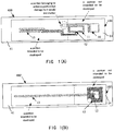
- Figure 1 is a top view showing the structure of a sticker with IC tag involved in the first embodiment of the present disclosure.
- Figure 1(A) shows a sticker with IC tag 400 in UHF band.
- Figure 1(B) shows a sticker with IC tag 400' in HF band.
- the sticker with IC tag 400 in UHF band comprises an IC tag insert 100, and a sheet-shaped tag paper 41 being a support for the sticker with IC tag 400.
- the IC tag insert 100 comprises: a radiation element 10 being an antenna; an impedance adjustment circuit 11, which adjusts the impedance matching of the antenna characteristics; an IC chip 12, an end of which is coupled to the impedance adjustment circuit 11; a disconnection detection circuit 13, which is coupled to the other end of the IC chip 12 and is constituted of a ring conductor; and a substrate 14, which is sheet-shaped and becomes a support for the radiation element 10, the impedance adjustment circuit 11, and the disconnection detection circuit 13.
- the radiation element 10 and the impedance adjustment circuit 11 form the antenna portion, which is used for communicating with an antenna of a reader (not illustrated).
- the portion on the left of the dashed line of the IC tag insert 100 in Figure 1(A) is a portion to be destroyed when opening a covered container 600 such as a wine bottle that has a sticker with IC tag adhered, and comprises a disconnection detection circuit 13.
- a portion on the right of the dashed line is a portion that is not intended to be destroyed when opening the covered container 600, and comprises a radiation element 10, an impedance adjustment circuit 11, and an IC chip 12.
- the radiation element 10 may also have a portion to which even a damage during opening would not matter. More specifically, the radiation element 10 is not intended to be destroyed. However, as long as the impedance adjustment circuit 11 is not cut off, communication may still be performed even through the best performance cannot be achieved. Therefore, it can be said that, even if the above portion surrounded by the circular dashed block is cut off in a scope that is not close to the impedance adjustment circuit 11, it would not matter.
- the sticker with IC tag 400' in HF band comprises an IC tag insert 100', and a sheet-shaped tag paper 41 being a support for the sticker with IC tag 400'.
- the IC tag insert 100' comprises: a loop circuit for antenna 15; an IC chip 12, an end of which is coupled to the loop circuit for antenna 15; a disconnection detection circuit 13, which is coupled to the other end of the IC chip 12 and is constituted of a ring conductor; and a substrate 14, which is sheet-shaped and becomes a support for the loop circuit for antenna 15 and the disconnection detection circuit 13.
- the loop circuit for antenna 15 forms the antenna portion, which is used for communicating with an antenna of a reader (not illustrated).
- portion on the left of the dashed line of the IC tag insert 100' in Figure 1(B) is a portion to be destroyed when opening a covered container 600, and comprises a disconnection detection circuit 13.
- a portion on the right of the dashed line is a portion that is not intended to be destroyed when opening the covered container 600, and comprises a loop circuit for antenna 15 and an IC chip 12.
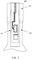
- FIG. 2 is a brief top view illustrating the adhereing method of a sticker with IC tag 400 involved in the present embodiment.
- the covered container 600 comprises a cover portion 610 and a container body 620.
- the covered container 600 is assumed to be a bottle with a metal cover that accommodates liquid such as vintage wine.
- the material of the cover portion 610 is assumed to be conductive materials such as aluminum.
- the sticker with IC tag 400 in UHF band is adhered to the covered container 600 so that the disconnection detection circuit 13 stretches across both the cover 610 and the container body 620.
- installation is made such that the impedance adjustment circuit 11 and the portion of the radiation element 10 that is close to the impedance adjustment circuit 11 do not stretch across both the cover portion 610 and the container body 620.
- the impedance adjustment circuit 11 and the portion of the radiation element 10 that is close to the impedance adjustment circuit 11 are installed on one side of the container body 620.
- the material of the cover portion 610 is not a conductive material but a non-conductive material such as plastic
- the impedance adjustment circuit 11 and the portion of the radiation element 10 that is close to the impedance adjustment circuit 11 may also be installed on one side of the cover portion 610.
- Figure 2 shows an adhering method of the sticker with IC tag 400 in UHF band.
- the sticker with IC tag 400' in HF band also has the following structure, that is, the disconnection detection circuit 13 stretching across both the cover 610 and the container body 620.
- FIG. 3 is a brief structural view of an IC chip 12 involved in the present embodiment.
- the IC chip 12 comprises: a communication functional portion, which is connected to the impedance adjustment circuit 11 (UHF band) or the loop circuit for antenna 15 (HF band) and has a function of communicating with a reader (now shown); and a disconnection detection functional portion, which is connected to the disconnection detection circuit 13 and has a function of detecting on and off of the disconnection detection circuit 13.
- the IC chip 12 utilizes UCODE G2iL+ produced by NXP Semiconductors Corporation, but is not limited to this.
- IC chips such as UCODE G2iM+ produced by NXP Semiconductors Corporation, NF4 by EM Microelectronic Corporation, etc. that detect disconnections using the resistance of the disconnection detection circuit other than antenna terminals may also be utilized.
- the sticker with IC tag of the present embodiment which has the above structures, comprises a disconnection detection circuit 13 that is installed in a manner that stretches across both the cover portion 610 and the container body 620.
- the IC chip 12 is connected to the disconnection detection circuit 13 and has a function of detecting on and off of the disconnection detection circuit 13.
- the impedance adjustment circuit 11 (UHF band) and the portion of the radiation element 10 that is close to the impedance adjustment circuit 11 , or the loop circuit for antenna 15 (HF band) are installed in a manner that do not stretch across both the cover portion 610 and the container body 620. Therefore, the disconnection detection circuit 13 may be reliably destroyed when opening the covered container 600, while the antenna portion is not destroyed but can continue communication.
- the opening status after opening the covered container may be identified, and a reader may be used to read individual numbers of the IC tag such as UID, EPC, etc. so that goods management, logistics management, and authenticity determination may be performed.
- Figure 4 is a conceptual diagram illustrating in detail the structure of the antenna portion of the sticker with IC tag involved in the present embodiment.
- the structure of Figure 4(A) corresponds to that of Figure 1(A) .
- the antenna portion is constituted by a radiation element 10 and an impedance adjustment circuit 11.
- the impedance adjustment circuit 11 is a loop-type impedance adjustment circuit, and is in electrical connection with the radiation element 10.
- the antenna portion is constituted by a radiation element 10 and an impedance adjustment circuit 11.
- the impedance adjustment circuit 11 is a loop-type impedance adjustment circuit, and is in electrical and physical connection with the radiation element 10.
- the antenna portion is constituted by an impedance adjustment circuit 11', which may also be a slot-type impedance adjustment circuit.
- the antenna portion may comprise radiation electrode 10 only but does not have an impedance adjustment circuit 11, where the radiation electrode 10 is directly connected to the IC chip 12.
- Figure 5(A) is a top view of the structure of the sticker with IC tag 400 in UHF band involved in the first embodiment.
- Figure 5(B) is a brief sectional view of the sticker with IC tag 400 in UHF band that is sectioned along the A-A line shown in Figure 5(A) .
- Figure 5(C) is a brief sectional view of the sticker with IC tag 400' in HF band.
- the sticker with IC tag has a structure wherein disconnection assistance machining is performed on the periphery of the disconnection detection circuit 13.
- the sticker with IC tag 400 in UHF band shown in Figure 5(B) comprises a tag paper 41.
- IC tag insert 100 is adhered to the back of the tag paper 41 with an adhesion layer 41 intervening.
- a conductive layer 43 which comprises the radiation element 10, the impedance adjustment circuit 11, and the disconnection detection circuit 13 shown in Figure 1(A) , is formed on one side of the substrate 14.
- An IC chip 12 is disposed on the conductive layer 43.
- An adhesion layer 45 is coated on and covering the remaining portion of the back of the tag paper 41 and on the IC tag insert 100.
- the sticker with IC tag 400' in HF band in Figure 5(C) differs from the sticker with IC tag 400 in UHF band in Figure 5(B) in the structure of the IC tag insert 100'.
- conductor layers 43 and 44 comprising the loop circuit for antenna 15 and the disconnection detection circuit 13 as shown in Figure 1(B) are respectively formed on two sides of the substrate 14, where an IC chip 12 is disposed on the conductor layer 43.
- the substrate 14 can be for example PET film.
- the conductor layers 43, 44 can be for example metal such as aluminum. Further, as desired or needed, trademarks or artistic patterns may also be printed on the surface of the tag paper 41.
- orientation of the IC tag insert 11 in Figures 5(B) and 5(C) is merely an example, an opposite orientation is possible.
- the following embodiments 2 to 4 have similar characteristics.
- a plurality of incisions 16 are formed on the substrate 14 and the tag paper 41 surrounding the disconnection detection circuit 13.
- the plurality of incisions 16 are formed for example from an end of the sticker with IC tag 400 towards the disconnection detection circuit 13. Further, disconnection assistance effects may be achieved even if the incisions 16 do not reach the disconnection detection circuit 13.
- the disconnection detection circuit 13 since the disconnection detection circuit 13 is easier to be disconnected as compared to the antenna portion during the opening, the disconnection detection circuit may be reliably destroyed while protecting the antenna portion.
- Figure 6(A) is a top view of the structure of the sticker with IC tag 400 in UHF band involved in the second embodiment.
- Figure 6(B) is a brief sectional view of the sticker with IC tag 400 in UHF band that is sectioned along the B-B line shown in Figure 6(A) .
- Figure 6(C) is a brief sectional view of the sticker with IC tag 400' in HF band.
- the sticker with IC tag 400 in UHF band shown in Figures 6(A) , 6(B) comprises a tag paper 41.
- IC tag insert 101 is adhered to the back of the tag paper 41 with an adhesion layer 42 intervening.
- a conductive layer 43 which comprises the radiation element 10, the impedance adjustment circuit 11, and the disconnection detection circuit 13 shown in Figure 1(A) , is formed on one side of the substrate 14'.
- An IC chip 12 is disposed on the conductive layer 43.
- An adhesion layer 45 is coated on the remaining portion of the back of the tag paper 41 and on the IC tag insert 101.
- the sticker with IC tag 400' in HF band in Figure 6(C) differs from the sticker with IC tag 400 in UHF band in Figure 6(B) in the structure of the IC tag insert 101'.
- conductor layers 43 and 44 comprising the loop circuit for antenna 15 and the disconnection detection circuit 13 as shown in Figure 1(B) are respectively formed on two sides of the substrate 14', where an IC chip 12 is disposed on the conductor layer 43.
- metal foils or metal ink may also be used as conductor layers 43 and 44.
- the substrate 14' is constituted by brittle materials such as paper, brittle film, etc.
- the IC tag inserts 101, 101' are constituted by a disconnection detection circuit and an antenna portion. To prevent the antenna portion being disconnected during the opening, enhanced machining shall be performed on the periphery of the antenna portion.
- an enhanced layer 46 is formed on the surface of the tag paper 41. Further, although not shown, the enhanced layer 46 may also be formed between the tag paper 41 and the antenna portion, for example between the tag paper 41 and the adhesion layer 42.
- a plurality of incisions may be formed on the substrate 14' and the tag paper 41.
- the second embodiment is similar to the first embodiment in that the disconnection detection circuit may be reliably destroyed during opening while protecting the antenna portion.
- Figure 7(A) is a top view of the structure of the sticker with IC tag 400 involved in the third embodiment.
- Figure 7(B) is a brief sectional view of the sticker with IC tag 400 that is sectioned along the C-C line shown in Figure 7(A) .
- the sticker with IC tag 400 comprises a tag paper 41.
- IC tag insert 102 is adhered to the back of the tag paper 41 with an adhesion layer 42 intervening.
- the IC tag insert 102 comprises a substrate 14' and a brittle layer 17.
- a conductive layer 43 which comprises a radiation element 10 and an impedance adjustment circuit 11, is formed on one side of the substrate 14'.
- a conductive layer 44 comprising a disconnection detection circuit 13 is formed on one side of the brittle layer 17.
- the other side of the substrate 14' is bonded with the other side of the brittle layer 17 so that the two may be easily stripped from each other.
- An IC chip 12 is disposed on the conductive layer 43.
- An adhesion layer 45 is coated on the remaining portion of the back of the tag paper 41 and on the IC tag insert 102.
- the IC tag insert 102 is constituted by a disconnection detection circuit and an antenna portion.
- the conductive layer 43 is disposed in the antenna portion, and the conductive layer 44 is disposed in the disconnection detection circuit.
- the tag paper 41 of the present embodiment may have the following structure: that is, a structure to avoid the strength being conducted on the boundary between the antenna portion and the disconnection detection circuit.
- the tag paper 400 have two breaches 18, which are approximately semi-circular, formed on the boundary between the antenna portion and the disconnection detection circuit.
- the disconnection detection circuit may be reliably destroyed during opening while protecting the antenna portion.
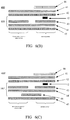
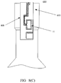
- Figures 8(A) to 8(C) are brief top views illustrating the adhering method of the sticker with IC tag 400 in UHF band involved in the second embodiment.
- Figures 9(A) to 9(C) are brief top views illustrating the adhering method of the sticker with IC tag 400' in HF band involved in the second embodiment.
- the covered container 600 in the present second embodiment is a wine bottle having a cover portion 610 constituted by metal materials such as metal heat shrinkable cap.
- the communication of the IC tag may sometimes be affected by the metal heat shrinkable cap due to the adhering position of the sticker with IC tag 400.
- the impedance adjustment circuit 11 does not coincide with the cover portion 610 at all. Therefore, communication is not affected, which is the ideal status.
- the cover portion 610 is constituted by metal materials, it is necessary to make at least a portion of the impedance adjustment circuit 11 not coincide with the cover portion 610 when installing the sticker with IC tag 400 to the covered container 600.
- the sticker with IC tag in the present embodiment is adhered outside of the metal heat shrinkable cap, but may also be adhered inside.
- the present disclosure is not only applicable to containers with high covers such as wine bottles, instead it is applicable to all containers with container body and cover.
- the shapes of these covered containers comprise for example a covered container 600 with a higher cover portion 610 as shown in Figure 10(A) and 10(C) , and a covered container 600' with a lower cover portion 610' as shown in Figure 10(B) and 10(D) .
- the method for adhering the sticker with IC tag to covered containers with various shapes will be illustrated with reference to Figures 10(A) to 10(D) .
- Figures 10(A) to 10(D) are brief perspective views illustrating the adhering method of the sticker with IC tag 400 involved in the third embodiment. Further, in Figures 10(A) to 10(D) , portions other than the disconnection detection portion 13 and the antenna portion 19 of the sticker with IC tag 400 are omitted in order to simplify explanation.
- the sticker with IC tag 400 is constituted by a higher cover portion 610 and a container body 620.
- the disconnection detection portion 13 is disposed on the side of the container body 620 and the side of the cover portion 610. Since the height of the cover portion 610 is relatively high, the disconnection detection portion 13 does not reach the top surface of the cover portion 610. Further, the antenna portion 19 is disposed on the container body 620 side.
- the sticker with IC tag 400 is constituted by a lower cover portion 610' and a container body 620'.
- the disconnection detection portion 13 is disposed from the side of the container body 620' and the side of the cover portion 610' to the top surface of the cover portion 610' since the height of the cover portion 610 is relatively low.
- the antenna portion 19 is disposed on the container body 620' side.
- the antenna portion 19 when installing the sticker with IC tag 400 to the covered containers 600, 600', the antenna portion 19 is disposed on container body 620, 620' side, but is not limited to this.
- the antenna portion 19 may be disposed on the cover portion 610, 610' side as shown in Figures 10(C) and 10(D) .
Landscapes
- Engineering & Computer Science (AREA)
- Microelectronics & Electronic Packaging (AREA)
- Computer Hardware Design (AREA)
- Physics & Mathematics (AREA)
- General Physics & Mathematics (AREA)
- Theoretical Computer Science (AREA)
- Mechanical Engineering (AREA)
- Computer Security & Cryptography (AREA)
- General Engineering & Computer Science (AREA)
- Computer Networks & Wireless Communication (AREA)
- Details Of Rigid Or Semi-Rigid Containers (AREA)
- Details Of Aerials (AREA)
- Closures For Containers (AREA)
Abstract
Description
- The present disclosure relates to a sticker with IC tag and the installation method thereof, and more specifically to a sticker with IC tag and the installation method thereof that may maintain the communication function of the IC tag and may detect the opening of a cover of a covered container such as a wine bottle when the cover is open.
- In the past, the demand in a worldwide scope for goods management, logistics management, and authenticity determination of goods such as wines is increasing. As an IC tag used for goods management, logistics management, and true and false management, an RFID tag is known for communicating with a reader in a contactless manner so as to transfer information between the reader and the tag itself. An RFID tag is composed of an RFIC chip for processing wireless signals, and an antenna for transmitting and receiving the wireless signals. Specified information is transmitted and received between the antenna of the RFID tag and the antenna of the reader as high frequency signals through a magnetic field or electric wave.
- However, in order to prevent the unlawful opening of the wine bottle or the repeated use of the IC tag, the IC tag should be destroyed when the wine bottle is opened.
- As a technique used to destroy the IC tag when opening the wine bottle as described above, for example, Patent Document 1 discloses the following sticker with IC tag and the adhering method thereof: that is, the antenna is installed as stretching across both a metal cover and a container body, the antenna is destroyed when the cover is opened, the opening of the metal cover is detected through the condition of the antenna being destroyed. In order to easily destroy the antenna easily when opening the cover, the sticker with IC tag in Patent Document 1 adopts the following structure: namely, a brittle processing for cutting off a slit (or loop circuit) for impedance matching adjustment of the antenna is carried out.
- Patent Document 1:
WO2006/016559 - However, while the sticker with IC tag of Patent Document 1 may detect the opening of a cover of a wine bottle by destroying an antenna containing an impedance adjustment circuit during the opening, communication cannot be continued after disconnection. On the other hand, there is a possibility of inability of communication under the circumstance that the IC tag has a malfunction. Therefore, it is uncertain whether the inability of communication is caused by the opening during normal use, or by the malfunction of the IC tag.
- In addition, if the IC tag cannot communicate, the information recorded in the IC tag (e.g., individual number) cannot be read, thus goods management or authenticity management cannot be performed after the opening.
- The present invention is accomplished in view of the above-mentioned problem, and its purpose is to provide a sticker with IC tag and the installation method thereof. The sticker with IC tag may detect the opening of a covered containing during the opening and may communicate even after the opening so that the information recorded in the IC tag may be read.
- To solve the above-mentioned technical problem, the present disclosure provides a sticker with IC tag comprising: an antenna portion; and an IC chip bonded with the antenna portion and having a function of communicating through the antenna portion. The sticker with IC tag is installed on a covered container, characterized in that the sticker with IC tag further comprises a disconnection detection portion which is constituted by a ring conductor. The disconnection detection portion is installed so as to stretch across both a cover of the covered container and a container body. The IC chip is connected to the disconnection detection portion and has a function of detecting the on and off of the disconnection detection portion.
- In addition, to solve the above-mentioned technical problem, an installation method of an sticker with IC tag involved in the present disclosure installs the sticker with IC tag to a covered container. The sticker with IC tag comprises: an antenna portion; and an IC chip bonded with the antenna portion and having a function of communicating through the antenna portion. The installation method of the sticker with IC tag is characterized in that the sticker with IC tag further comprises a disconnection detection portion which is constituted by a ring conductor. The IC chip is connected to the disconnection detection portion and has a function of detecting the on and off of the disconnection detection portion. When installing the sticker with IC tag to the covered container, the disconnection detection portion is installed so as to stretch across both a cover of the covered container and a container body.
- According to the present disclosure, the following effects are achieved: since the IC tag identifies the opening (disconnection) of the covered container by merely cutting off the disconnection detection portion, communication with a reader can be performed even if the disconnection detection portion is cut off so that the reader can be used to read individual identification numbers such as the UID (User Identifier), EPC (Electric Product Code), etc. of the IC tag even after the opening.
-
-
Figure 1(A) is a top view showing the structure of a sticker with IC tag in UHF band involved in the first embodiment of the present disclosure.Figure 1(B) is a top view showing the structure of a sticker with IC tag in HF band. -
Figure 2 is a brief top view illustrating the adhering method of a sticker with IC tag involved in the first embodiment of the present disclosure. -
Figure 3 is a brief structural view of a sticker with IC tag involved in the first embodiment of the present disclosure. -
Figures 4(A) to 4(D) are conceptual diagrams illustrating in detail the structure of the antenna portion of the sticker with IC tag involved in the first embodiment of the present disclosure. -
Figure 5(A) is a top view of the structure of the sticker with IC tag in UHF band involved in the first embodiment of the present disclosure.Figure 5(B) is a brief sectional view of the sticker with IC tag in UHF band that is sectioned along the A-A line shown inFigure 5(A) .Figure 5(C) is a brief sectional view of the sticker with IC tag in HF band. -
Figure 6(A) is a top view of the structure of the sticker with IC tag in UHF band involved in the second embodiment of the present disclosure.Figure 6(B) is a brief sectional view of the sticker with IC tag in UHF band that is sectioned along the B-B line shown inFigure 6(A) .Figure 6(C) is a brief sectional view of the sticker with IC tag in HF band. -
Figure 7(A) is a top view of the structure of the sticker with IC tag involved in the third embodiment of the present disclosure.Figure 7(B) is a brief sectional view of the sticker with IC tag that is sectioned along the C-C line shown inFigure 7(A) . -
Figures 8(A) to 8(C) are brief top views illustrating the adhering method of the sticker with IC tag in UHF band involved in the second embodiment of the present disclosure. -
Figures 9(A) to 9(C) are brief top views illustrating the adhering method of the sticker with IC tag in HF band involved in the second embodiment of the present disclosure. -
Figures 10(A) to 10(D) are brief perspective views illustrating the adhering method of the sticker with IC tag involved in the third embodiment of the present disclosure. - In the following descriptions, the first embodiment of the present disclosure will be explained with reference to
Figures 1 to 4 . -
Figure 1 is a top view showing the structure of a sticker with IC tag involved in the first embodiment of the present disclosure.Figure 1(A) shows a sticker withIC tag 400 in UHF band.Figure 1(B) shows a sticker with IC tag 400' in HF band. - As shown in
Figure 1(A) , the sticker withIC tag 400 in UHF band comprises anIC tag insert 100, and a sheet-shaped tag paper 41 being a support for the sticker withIC tag 400. The IC tag insert 100 comprises: aradiation element 10 being an antenna; animpedance adjustment circuit 11, which adjusts the impedance matching of the antenna characteristics; anIC chip 12, an end of which is coupled to theimpedance adjustment circuit 11; adisconnection detection circuit 13, which is coupled to the other end of theIC chip 12 and is constituted of a ring conductor; and asubstrate 14, which is sheet-shaped and becomes a support for theradiation element 10, theimpedance adjustment circuit 11, and thedisconnection detection circuit 13. In addition, theradiation element 10 and theimpedance adjustment circuit 11 form the antenna portion, which is used for communicating with an antenna of a reader (not illustrated). - In addition, the portion on the left of the dashed line of the IC tag insert 100 in
Figure 1(A) is a portion to be destroyed when opening a coveredcontainer 600 such as a wine bottle that has a sticker with IC tag adhered, and comprises adisconnection detection circuit 13. A portion on the right of the dashed line is a portion that is not intended to be destroyed when opening the coveredcontainer 600, and comprises aradiation element 10, animpedance adjustment circuit 11, and anIC chip 12. - In addition, as shown by the portion surrounded by a circular dashed block in
Figure 1(A) , theradiation element 10 may also have a portion to which even a damage during opening would not matter. More specifically, theradiation element 10 is not intended to be destroyed. However, as long as theimpedance adjustment circuit 11 is not cut off, communication may still be performed even through the best performance cannot be achieved. Therefore, it can be said that, even if the above portion surrounded by the circular dashed block is cut off in a scope that is not close to theimpedance adjustment circuit 11, it would not matter. - As shown in
Figure 1(B) , the sticker with IC tag 400' in HF band comprises an IC tag insert 100', and a sheet-shaped tag paper 41 being a support for the sticker with IC tag 400'. The IC tag insert 100' comprises: a loop circuit forantenna 15; anIC chip 12, an end of which is coupled to the loop circuit forantenna 15; adisconnection detection circuit 13, which is coupled to the other end of theIC chip 12 and is constituted of a ring conductor; and asubstrate 14, which is sheet-shaped and becomes a support for the loop circuit forantenna 15 and thedisconnection detection circuit 13. In addition, the loop circuit forantenna 15 forms the antenna portion, which is used for communicating with an antenna of a reader (not illustrated). - Further, the portion on the left of the dashed line of the IC tag insert 100' in
Figure 1(B) is a portion to be destroyed when opening a coveredcontainer 600, and comprises adisconnection detection circuit 13. A portion on the right of the dashed line is a portion that is not intended to be destroyed when opening the coveredcontainer 600, and comprises a loop circuit forantenna 15 and anIC chip 12. - Next, the adhering method of the sticker with IC tag of the present disclosure is described.
-
Figure 2 is a brief top view illustrating the adhereing method of a sticker withIC tag 400 involved in the present embodiment. The coveredcontainer 600 comprises acover portion 610 and acontainer body 620. In the present embodiment, the coveredcontainer 600 is assumed to be a bottle with a metal cover that accommodates liquid such as vintage wine. In addition, the material of thecover portion 610 is assumed to be conductive materials such as aluminum. - As shown in
Figure 2 , the sticker withIC tag 400 in UHF band is adhered to the coveredcontainer 600 so that thedisconnection detection circuit 13 stretches across both thecover 610 and thecontainer body 620. - In the present embodiment, installation is made such that the
impedance adjustment circuit 11 and the portion of theradiation element 10 that is close to theimpedance adjustment circuit 11 do not stretch across both thecover portion 610 and thecontainer body 620. Theimpedance adjustment circuit 11 and the portion of theradiation element 10 that is close to theimpedance adjustment circuit 11 are installed on one side of thecontainer body 620. However, in the case that for example the material of thecover portion 610 is not a conductive material but a non-conductive material such as plastic, theimpedance adjustment circuit 11 and the portion of theradiation element 10 that is close to theimpedance adjustment circuit 11 may also be installed on one side of thecover portion 610. - Further,
Figure 2 shows an adhering method of the sticker withIC tag 400 in UHF band. In addition, although not shown, the sticker with IC tag 400' in HF band also has the following structure, that is, thedisconnection detection circuit 13 stretching across both thecover 610 and thecontainer body 620. - Next, the brief structure of the IC chip of the present embodiment is described.
-
Figure 3 is a brief structural view of anIC chip 12 involved in the present embodiment. TheIC chip 12 comprises: a communication functional portion, which is connected to the impedance adjustment circuit 11 (UHF band) or the loop circuit for antenna 15 (HF band) and has a function of communicating with a reader (now shown); and a disconnection detection functional portion, which is connected to thedisconnection detection circuit 13 and has a function of detecting on and off of thedisconnection detection circuit 13. - In addition, in the present embodiment, the
IC chip 12 utilizes UCODE G2iL+ produced by NXP Semiconductors Corporation, but is not limited to this. IC chips such as UCODE G2iM+ produced by NXP Semiconductors Corporation, NF4 by EM Microelectronic Corporation, etc. that detect disconnections using the resistance of the disconnection detection circuit other than antenna terminals may also be utilized. - The sticker with IC tag of the present embodiment, which has the above structures, comprises a
disconnection detection circuit 13 that is installed in a manner that stretches across both thecover portion 610 and thecontainer body 620. TheIC chip 12 is connected to thedisconnection detection circuit 13 and has a function of detecting on and off of thedisconnection detection circuit 13. The impedance adjustment circuit 11 (UHF band) and the portion of theradiation element 10 that is close to theimpedance adjustment circuit 11 , or the loop circuit for antenna 15 (HF band) are installed in a manner that do not stretch across both thecover portion 610 and thecontainer body 620. Therefore, thedisconnection detection circuit 13 may be reliably destroyed when opening the coveredcontainer 600, while the antenna portion is not destroyed but can continue communication. Thus, the opening status after opening the covered container may be identified, and a reader may be used to read individual numbers of the IC tag such as UID, EPC, etc. so that goods management, logistics management, and authenticity determination may be performed. - Next, the structure of the antenna portion of the sticker with IC tag involved in the present embodiment is described in detail.
-
Figure 4 is a conceptual diagram illustrating in detail the structure of the antenna portion of the sticker with IC tag involved in the present embodiment. The structure ofFigure 4(A) corresponds to that ofFigure 1(A) . As shown inFigure 4(A) , the antenna portion is constituted by aradiation element 10 and animpedance adjustment circuit 11. Theimpedance adjustment circuit 11 is a loop-type impedance adjustment circuit, and is in electrical connection with theradiation element 10. - Further, as shown in
Figure 4(B) , the antenna portion is constituted by aradiation element 10 and animpedance adjustment circuit 11. Theimpedance adjustment circuit 11 is a loop-type impedance adjustment circuit, and is in electrical and physical connection with theradiation element 10. - Further, as shown in
Figure 4(C) , the antenna portion is constituted by an impedance adjustment circuit 11', which may also be a slot-type impedance adjustment circuit. - Further, as shown in
Figure 4(D) , the antenna portion may compriseradiation electrode 10 only but does not have animpedance adjustment circuit 11, where theradiation electrode 10 is directly connected to theIC chip 12. - In the following description, the first through third embodiments of the present disclosure will be explained with reference to
Figures 5 to 6 . -
Figure 5(A) is a top view of the structure of the sticker withIC tag 400 in UHF band involved in the first embodiment.Figure 5(B) is a brief sectional view of the sticker withIC tag 400 in UHF band that is sectioned along the A-A line shown inFigure 5(A) .Figure 5(C) is a brief sectional view of the sticker with IC tag 400' in HF band. - When opening the covered container, it is required to make the
disconnection detection circuit 13 easy to be disconnected. Therefore, the sticker with IC tag has a structure wherein disconnection assistance machining is performed on the periphery of thedisconnection detection circuit 13. - The sticker with
IC tag 400 in UHF band shown inFigure 5(B) comprises atag paper 41.IC tag insert 100 is adhered to the back of thetag paper 41 with anadhesion layer 41 intervening. In theIC tag insert 100, aconductive layer 43, which comprises theradiation element 10, theimpedance adjustment circuit 11, and thedisconnection detection circuit 13 shown inFigure 1(A) , is formed on one side of thesubstrate 14. AnIC chip 12 is disposed on theconductive layer 43. Anadhesion layer 45 is coated on and covering the remaining portion of the back of thetag paper 41 and on theIC tag insert 100. - The sticker with IC tag 400' in HF band in
Figure 5(C) differs from the sticker withIC tag 400 in UHF band inFigure 5(B) in the structure of the IC tag insert 100'. In the IC tag insert 100', conductor layers 43 and 44 comprising the loop circuit forantenna 15 and thedisconnection detection circuit 13 as shown inFigure 1(B) are respectively formed on two sides of thesubstrate 14, where anIC chip 12 is disposed on theconductor layer 43. - Further, in the present embodiment, the
substrate 14 can be for example PET film. The conductor layers 43, 44 can be for example metal such as aluminum. Further, as desired or needed, trademarks or artistic patterns may also be printed on the surface of thetag paper 41. - Further, the orientation of the
IC tag insert 11 inFigures 5(B) and5(C) is merely an example, an opposite orientation is possible. The following embodiments 2 to 4 have similar characteristics. - In the present embodiment, as an example of the disconnection assistance machining, as shown in
Figure 5(A) , a plurality ofincisions 16 are formed on thesubstrate 14 and thetag paper 41 surrounding thedisconnection detection circuit 13. The plurality ofincisions 16 are formed for example from an end of the sticker withIC tag 400 towards thedisconnection detection circuit 13. Further, disconnection assistance effects may be achieved even if theincisions 16 do not reach thedisconnection detection circuit 13. - According to the present first embodiment, since the
disconnection detection circuit 13 is easier to be disconnected as compared to the antenna portion during the opening, the disconnection detection circuit may be reliably destroyed while protecting the antenna portion. -
Figure 6(A) is a top view of the structure of the sticker withIC tag 400 in UHF band involved in the second embodiment.Figure 6(B) is a brief sectional view of the sticker withIC tag 400 in UHF band that is sectioned along the B-B line shown inFigure 6(A) .Figure 6(C) is a brief sectional view of the sticker with IC tag 400' in HF band. - The sticker with
IC tag 400 in UHF band shown inFigures 6(A) ,6(B) comprises atag paper 41.IC tag insert 101 is adhered to the back of thetag paper 41 with anadhesion layer 42 intervening. In theIC tag insert 101, aconductive layer 43, which comprises theradiation element 10, theimpedance adjustment circuit 11, and thedisconnection detection circuit 13 shown inFigure 1(A) , is formed on one side of the substrate 14'. AnIC chip 12 is disposed on theconductive layer 43. Anadhesion layer 45 is coated on the remaining portion of the back of thetag paper 41 and on theIC tag insert 101. - The sticker with IC tag 400' in HF band in
Figure 6(C) differs from the sticker withIC tag 400 in UHF band inFigure 6(B) in the structure of the IC tag insert 101'. In the IC tag insert 101', conductor layers 43 and 44 comprising the loop circuit forantenna 15 and thedisconnection detection circuit 13 as shown inFigure 1(B) are respectively formed on two sides of the substrate 14', where anIC chip 12 is disposed on theconductor layer 43. - Further, metal foils or metal ink, for example, may also be used as conductor layers 43 and 44.
- In the present embodiment, as another example of disconnection assistance machining, the substrate 14' is constituted by brittle materials such as paper, brittle film, etc.
- Further, as shown in
Figures 6(A) to 6(C) , in the present embodiment, the IC tag inserts 101, 101' are constituted by a disconnection detection circuit and an antenna portion. To prevent the antenna portion being disconnected during the opening, enhanced machining shall be performed on the periphery of the antenna portion. - As an example of the enhanced machining, for example as shown in
Figures 6(B) and 6(C) , for the antenna portion of the IC tag inserts 101, 101', anenhanced layer 46 is formed on the surface of thetag paper 41. Further, although not shown, the enhancedlayer 46 may also be formed between thetag paper 41 and the antenna portion, for example between thetag paper 41 and theadhesion layer 42. - Further, in the present second embodiment, similarly as in the first embodiment, a plurality of incisions may be formed on the substrate 14' and the
tag paper 41. - The second embodiment is similar to the first embodiment in that the disconnection detection circuit may be reliably destroyed during opening while protecting the antenna portion.
-
Figure 7(A) is a top view of the structure of the sticker withIC tag 400 involved in the third embodiment.Figure 7(B) is a brief sectional view of the sticker withIC tag 400 that is sectioned along the C-C line shown inFigure 7(A) . - As shown in
Figure 7(B) , the sticker withIC tag 400 comprises atag paper 41.IC tag insert 102 is adhered to the back of thetag paper 41 with anadhesion layer 42 intervening. TheIC tag insert 102 comprises a substrate 14' and abrittle layer 17. Aconductive layer 43, which comprises aradiation element 10 and animpedance adjustment circuit 11, is formed on one side of the substrate 14'. Aconductive layer 44 comprising adisconnection detection circuit 13 is formed on one side of thebrittle layer 17. The other side of the substrate 14' is bonded with the other side of thebrittle layer 17 so that the two may be easily stripped from each other. AnIC chip 12 is disposed on theconductive layer 43. Anadhesion layer 45 is coated on the remaining portion of the back of thetag paper 41 and on theIC tag insert 102. - Further, as shown in
Figure 7(A) and 7(B) , in the present embodiment, theIC tag insert 102 is constituted by a disconnection detection circuit and an antenna portion. Theconductive layer 43 is disposed in the antenna portion, and theconductive layer 44 is disposed in the disconnection detection circuit. - In the present embodiment, when opening a covered container, if it is intended to strip off the
tag paper 41 from the side of the disconnection detection circuit (left side shown inFigure 7(B) ), the substrate 14' is separated from thebrittle layer 17, and thedisconnection detection circuit 13 is destroyed at the first place. - However, if stripping continues, strength will be conducted to the antenna portion so that the antenna portion would possibly be destroyed. As an enhanced machining for addressing the above issue, as shown in
Figure 7(A) , thetag paper 41 of the present embodiment may have the following structure: that is, a structure to avoid the strength being conducted on the boundary between the antenna portion and the disconnection detection circuit. As an example of the structure, thetag paper 400 have twobreaches 18, which are approximately semi-circular, formed on the boundary between the antenna portion and the disconnection detection circuit. - According to the above structure, the disconnection detection circuit may be reliably destroyed during opening while protecting the antenna portion.
- In the following description, the second embodiment of the present disclosure will be explained with reference to
Figures 8 to 9 . -
Figures 8(A) to 8(C) are brief top views illustrating the adhering method of the sticker withIC tag 400 in UHF band involved in the second embodiment.Figures 9(A) to 9(C) are brief top views illustrating the adhering method of the sticker with IC tag 400' in HF band involved in the second embodiment. - The covered
container 600 in the present second embodiment is a wine bottle having acover portion 610 constituted by metal materials such as metal heat shrinkable cap. In this case, the communication of the IC tag may sometimes be affected by the metal heat shrinkable cap due to the adhering position of the sticker withIC tag 400. - First, if the sticker with
IC tag 400 is installed to the coveredcontainer 600 as shown inFigure 8(A) , theimpedance adjustment circuit 11 does not coincide with thecover portion 610 at all. Therefore, communication is not affected, which is the ideal status. - Next, if the sticker with
IC tag 400 is installed to the coveredcontainer 600 as shown inFigure 8(B) , a portion of theimpedance adjustment circuit 11 coincides with thecover portion 610. In this case, communication may still be continued, which is also fine. - Then, if the sticker with
IC tag 400 is installed to the coveredcontainer 600 as shown inFigure 8(C) , theimpedance adjustment circuit 11 is completely shielded by thecover portion 610. Therefore, communication cannot be performed. - Therefore, in case that the
cover portion 610 is constituted by metal materials, it is necessary to make at least a portion of theimpedance adjustment circuit 11 not coincide with thecover portion 610 when installing the sticker withIC tag 400 to the coveredcontainer 600. - Further, for reasons similar to the above, when installing the sticker with IC tag 400' in HF band to the covered
container 600 as shown inFigures 9(A) to 9(C) , it is necessary to make at least a portion of the loop circuit forantenna 15 not coincide with thecover portion 610. - Further, the sticker with IC tag in the present embodiment is adhered outside of the metal heat shrinkable cap, but may also be adhered inside.
- The present disclosure is not only applicable to containers with high covers such as wine bottles, instead it is applicable to all containers with container body and cover. The shapes of these covered containers comprise for example a covered
container 600 with ahigher cover portion 610 as shown inFigure 10(A) and10(C) , and a covered container 600' with a lower cover portion 610' as shown inFigure 10(B) and10(D) . In the following description, the method for adhering the sticker with IC tag to covered containers with various shapes will be illustrated with reference toFigures 10(A) to 10(D) . -
Figures 10(A) to 10(D) are brief perspective views illustrating the adhering method of the sticker withIC tag 400 involved in the third embodiment. Further, inFigures 10(A) to 10(D) , portions other than thedisconnection detection portion 13 and theantenna portion 19 of the sticker withIC tag 400 are omitted in order to simplify explanation. - First, as shown in
Figure 10(A) , the sticker withIC tag 400 is constituted by ahigher cover portion 610 and acontainer body 620. When installing the sticker withIC tag 400 to the coveredcontainer 600, thedisconnection detection portion 13 is disposed on the side of thecontainer body 620 and the side of thecover portion 610. Since the height of thecover portion 610 is relatively high, thedisconnection detection portion 13 does not reach the top surface of thecover portion 610. Further, theantenna portion 19 is disposed on thecontainer body 620 side. - Next, as shown in
Figure 10(B) , the sticker withIC tag 400 is constituted by a lower cover portion 610' and acontainer body 620'. When installing the sticker withIC tag 400 to the covered container 600', thedisconnection detection portion 13 is disposed from the side of thecontainer body 620' and the side of the cover portion 610' to the top surface of the cover portion 610' since the height of thecover portion 610 is relatively low. Further, theantenna portion 19 is disposed on thecontainer body 620' side. - Further, in
Figures 10(A) and 10(B) , when installing the sticker withIC tag 400 to the coveredcontainers 600, 600', theantenna portion 19 is disposed oncontainer body antenna portion 19 may be disposed on thecover portion 610, 610' side as shown inFigures 10(C) and 10(D) . - The embodiments and varied embodiments of the present disclosure are illustrated above. However, various omissions, replacements, and modifications may be made within the scope of the idea of the present disclosure.
-
- 10 Radiation element (Antenna)
- 11, 11' Impedance adjustment circuit
- 12 IC chip
- 13 Disconnection detection circuit (Disconnection detection portion)
- 14, 14' Substrate
- 15 Loop circuit for antenna
- 16 Incision
- 17 Brittle layer
- 18 Breach
- 19 Antenna portion
- 41 Tag paper (Tag portion)
- 42, 45 Adhesion layer
- 43, 44 Conductor layer
- 46 Enhanced layer
- 100, 100', 101, 101', 102 IC Tag insert
- 400, 400' sticker with IC tag
- 600, 600' Covered container
- 610, 610' Cover portion
- 620, 620' Container body
Claims (14)
- A sticker with IC tag comprising: an antenna portion; and an IC chip coupled to the antenna portion and having a function of communicating through the antenna portion, the sticker with IC tag being installed on a covered container, characterized in that,
the sticker with IC tag further comprises a disconnection detection portion, which is constituted by a ring conductor, the disconnection detection portion being installed so as to stretch across both a cover portion and a container body,
the IC chip being connected to the disconnection detection portion and having a function of detecting on and off of the disconnection detection portion. - The sticker with IC tag as recited in claim 1, wherein,
disconnection assistance machining is performed on the periphery of the disconnection detection portion so that the disconnection detection portion becomes easy to be disconnected when opening the covered container. - The sticker with IC tag as recited in claim 2, wherein,
the sticker with IC tag further comprises:a substrate, being sheet-shaped and being a support for the antenna portion and the disconnection detection portion; anda tag portion, being sheet-shaped and being a support for the sticker with IC tag,wherein as the disconnection assistance machining, a plurality of incisions are formed on the substrate at periphery of the disconnection detection portion and on the tag portion. - The sticker with IC tag as recited in claim 2, wherein,
the sticker with IC tag further comprises:a substrate, being sheet-shaped and being a support for the antenna portion and the disconnection detection portion; anda tag portion, being sheet-shaped and being a support for the sticker with IC tag,wherein as the disconnection assistance machining, the substrate at periphery of the disconnection detection portion being constituted by brittle materials. - The sticker with IC tag as recited in any of claims 1 to 4, wherein,
enhanced machining is performed on the periphery of the antenna portion so that the antenna portion is not easily disconnected. - The sticker with IC tag as recited in claim 5, wherein,
as the enhanced machining, the tag portion has the following structure, that is, a structure to avoid strength being conducted on the boundary between the antenna portion and the disconnection detection portion. - The sticker with IC tag as recited in claim 5, wherein,
as the enhanced machining, an enhanced layer is formed in the area of the antenna portion that is on the surface of the tag portion or between the tag portion and the antenna portion. - An installation method for a sticker with IC tag, to install the sticker with IC tag to a covered container, the sticker with IC tag comprising: an antenna portion; and an IC chip coupled to the antenna portion and having a function of communicating through the antenna portion, the installation method for the sticker with IC tag is characterized in that,
the sticker with IC tag further comprises a disconnection detection portion, which is constituted by a ring conductor,
the IC chip being connected to the disconnection detection portion and having a function of detecting on and off of the disconnection detection portion,
when installing the sticker with IC tag to the covered container, the disconnection detection portion is installed so as to stretch across both a cover portion and a container body. - The installation method for the sticker with IC tag as recited in claim 8, wherein,
when installing the sticker with IC tag to the covered container, the disconnection detection portion is disposed on the side of the container body and the side of the cover portion. - The installation method for the sticker with IC tag as recited in claim 8, wherein,
when installing the sticker with IC tag to the covered container, the disconnection detection portion is disposed from the side of the container body and the side of the cover portion to the top surface of the cover portion. - The installation method for the sticker with IC tag as recited in any of claims 8 to 10, wherein the antenna portion is disposed on the container body side.
- The installation method for the sticker with IC tag as recited in any of claims 8 to 10, wherein the antenna portion is disposed on the cover portion side.
- The installation method for the sticker with IC tag as recited in claim 8, wherein,
the antenna portion comprises an impedance adjustment circuit or a loop circuit for antenna, wherein the impedance adjustment circuit being used for impedance matching of the antenna characteristics,
the cover portion being a metal heat shrinkable cap,
the sticker with IC tag being installed so that at least a portion of the impedance adjustment circuit or at least a portion of the loop circuit for antenna does not coincide with the metal heat shrinkable cap. - A covered container having a sticker with IC tag as recited in any of claims 1 to 7 installed thereon.
Applications Claiming Priority (2)
| Application Number | Priority Date | Filing Date | Title |
|---|---|---|---|
| CN201510566380.XA CN106503778A (en) | 2015-09-08 | 2015-09-08 | Band IC tag paster and its installation method |
| PCT/CN2016/098404 WO2017041724A1 (en) | 2015-09-08 | 2016-09-08 | Sticker having ic tag, and mounting method thereof |
Publications (3)
| Publication Number | Publication Date |
|---|---|
| EP3348490A1 true EP3348490A1 (en) | 2018-07-18 |
| EP3348490A4 EP3348490A4 (en) | 2019-03-27 |
| EP3348490B1 EP3348490B1 (en) | 2022-11-23 |
Family
ID=58240563
Family Applications (1)
| Application Number | Title | Priority Date | Filing Date |
|---|---|---|---|
| EP16843662.4A Active EP3348490B1 (en) | 2015-09-08 | 2016-09-08 | Sticker having ic tag, and mounting method thereof |
Country Status (5)
| Country | Link |
|---|---|
| US (1) | US10489699B2 (en) |
| EP (1) | EP3348490B1 (en) |
| JP (1) | JP6973379B2 (en) |
| CN (2) | CN106503778A (en) |
| WO (1) | WO2017041724A1 (en) |
Cited By (4)
| Publication number | Priority date | Publication date | Assignee | Title |
|---|---|---|---|---|
| WO2020179924A1 (en) * | 2019-03-07 | 2020-09-10 | Otsuka Pharmaceutical Co., Ltd. | Methods and apparatus for activation of a wearable patch |
| FR3106425A1 (en) * | 2020-01-20 | 2021-07-23 | Safran Aircraft Engines | Radio frequency label comprising a means of destruction and associated method |
| EP4220482A1 (en) * | 2019-11-16 | 2023-08-02 | Avery Dennison Retail Information Services LLC | Rfid and packaging substrate systems and methods |
| US12383181B2 (en) | 2019-01-24 | 2025-08-12 | Otsuka Pharmaceutical Co, Ltd. | Elastic wearable sensor |
Families Citing this family (16)
| Publication number | Priority date | Publication date | Assignee | Title |
|---|---|---|---|---|
| JP7183791B2 (en) * | 2017-10-04 | 2022-12-06 | 東レ株式会社 | Packaging material and method for manufacturing packaging material |
| JP2019078611A (en) * | 2017-10-24 | 2019-05-23 | 川崎重工業株式会社 | Fastening member looseness detection tag |
| JP2020101978A (en) * | 2018-12-21 | 2020-07-02 | トッパン・フォームズ株式会社 | Looseness detection label and looseness detection method using the same |
| JP2020101979A (en) * | 2018-12-21 | 2020-07-02 | トッパン・フォームズ株式会社 | RFID label and state detection method using the same |
| JP7221099B2 (en) * | 2019-03-19 | 2023-02-13 | トッパン・フォームズ株式会社 | Looseness detection label |
| JP7412220B2 (en) * | 2019-03-19 | 2024-01-12 | Toppanエッジ株式会社 | Looseness detection label and looseness detection structure |
| JP7212561B2 (en) * | 2019-03-19 | 2023-01-25 | トッパン・フォームズ株式会社 | Looseness detection label |
| JP7212562B2 (en) * | 2019-03-19 | 2023-01-25 | トッパン・フォームズ株式会社 | Looseness detection label |
| WO2020189474A1 (en) * | 2019-03-19 | 2020-09-24 | トッパン・フォームズ株式会社 | Looseness detection label and looseness detection structure |
| JP2021002196A (en) * | 2019-06-21 | 2021-01-07 | 凸版印刷株式会社 | Ic tag label and easy-peel container |
| JP2021111252A (en) * | 2020-01-15 | 2021-08-02 | 大日本印刷株式会社 | Anti-theft tag label |
| JP7470526B2 (en) * | 2020-02-19 | 2024-04-18 | 大王製紙株式会社 | RFID tag and antenna |
| JP7475914B2 (en) * | 2020-03-24 | 2024-04-30 | サトーホールディングス株式会社 | RFID label and method for manufacturing the same |
| JP2022000677A (en) * | 2020-06-19 | 2022-01-04 | 凸版印刷株式会社 | Sealing sticker with ic tag and container |
| US12124905B1 (en) * | 2021-12-17 | 2024-10-22 | Wells Fargo Bank, N.A. | Transaction instrument with features for destruction and disposal |
| JP7605269B1 (en) | 2023-09-27 | 2024-12-24 | いすゞ自動車株式会社 | Detection System |
Family Cites Families (47)
| Publication number | Priority date | Publication date | Assignee | Title |
|---|---|---|---|---|
| US5126749A (en) | 1989-08-25 | 1992-06-30 | Kaltner George W | Individually fed multiloop antennas for electronic security systems |
| CA2125786C (en) * | 1991-12-19 | 2007-07-31 | Ake Gustafson | Security sealing device |
| DE19720747C2 (en) * | 1996-05-24 | 2003-04-10 | Sokymat Identifikations Kompon | Security element containing a transponder |
| JP3911900B2 (en) * | 1999-04-05 | 2007-05-09 | 株式会社日立製作所 | IC seal |
| DE10012204A1 (en) | 2000-03-13 | 2001-09-20 | Siemens Ag | Electronic postage stamp for identifying postal articles |
| JP4590161B2 (en) | 2001-05-21 | 2010-12-01 | スコット・ラボラトリーズ・インコーポレイテッド | RF-ID label for medical container |
| ITMI20022121A1 (en) | 2002-10-04 | 2004-04-05 | Fidereveuropa | ELECTRONIC PAPER WITH AT LEAST ONE ADHESIVE SURFACE. |
| ATE530998T1 (en) * | 2003-07-07 | 2011-11-15 | Avery Dennison Corp | RFID DEVICE WITH CHANGEABLE CHARACTERISTICS |
| CN1898686A (en) | 2003-12-24 | 2007-01-17 | 新加坡科技物资管理私人有限公司 | Rfid sealing label |
| US7098794B2 (en) * | 2004-04-30 | 2006-08-29 | Kimberly-Clark Worldwide, Inc. | Deactivating a data tag for user privacy or tamper-evident packaging |
| JP3105286U (en) | 2004-05-17 | 2004-10-28 | 富士光電株式会社 | Structure of a container having a feature that a wireless IC tag is destroyed during use |
| CN101001792B (en) * | 2004-08-09 | 2011-03-30 | 凸版印刷株式会社 | Seal with IC label and its installation method |
| US20060145870A1 (en) | 2004-10-19 | 2006-07-06 | Coveley Michael E | Container including a tamper-resistant seal and to a radio frequency identification seal |
| JP2006123917A (en) | 2004-10-26 | 2006-05-18 | Mitsubishi Materials Corp | Sealing structure, opening discrimination method, and tag |
| JP4562491B2 (en) * | 2004-10-26 | 2010-10-13 | 京セラ株式会社 | Transmission control device |
| JP2006184082A (en) | 2004-12-27 | 2006-07-13 | Hitachi Ltd | Sealing method and sealing confirmation system for radioactive material storage container |
| US20060152364A1 (en) * | 2004-12-30 | 2006-07-13 | Walton Charles A | RFID with field changeable identification |
| JP4453582B2 (en) * | 2005-03-16 | 2010-04-21 | 富士通株式会社 | RFID tag |
| US20060214789A1 (en) * | 2005-03-24 | 2006-09-28 | Joshua Posamentier | Tamper detection with RFID tag |
| JP4815891B2 (en) * | 2005-06-22 | 2011-11-16 | 株式会社日立製作所 | Wireless IC tag and antenna manufacturing method |
| JP4826195B2 (en) | 2005-09-30 | 2011-11-30 | 大日本印刷株式会社 | RFID tag |
| JP2007122466A (en) * | 2005-10-28 | 2007-05-17 | Fujitsu Ltd | RFID tag |
| US7388506B2 (en) | 2006-02-07 | 2008-06-17 | Rexam Healthcare Packaging Inc. | Closure and package with induction seal and RFID tag |
| US7410103B2 (en) * | 2006-03-13 | 2008-08-12 | Andreas Rolf Nagel | System, method and device to detect product tampering |
| JP2008143589A (en) | 2006-12-13 | 2008-06-26 | Dainippon Printing Co Ltd | Packaging package with IC tag |
| JP2009001326A (en) * | 2007-06-25 | 2009-01-08 | Nec Corp | Cap |
| US7898422B2 (en) | 2007-10-18 | 2011-03-01 | Wine Father LLC | Tamper-resistant microchip assembly |
| WO2009050662A1 (en) | 2007-10-19 | 2009-04-23 | Petratec International Ltd. | Rfid tag especially for use near conductive objects |
| JP2009150915A (en) * | 2007-10-19 | 2009-07-09 | Imai Toshiki | Sealing sticker |
| EP2301857B1 (en) | 2008-06-20 | 2012-08-29 | Toyo Seikan Kaisha, Ltd. | Resin overcap provided with ic tag |
| JP5639606B2 (en) | 2012-02-27 | 2014-12-10 | 三智商事株式会社 | Wireless IC tag |
| CN202529311U (en) | 2012-04-05 | 2012-11-14 | 四川省宜宾五粮液集团有限公司 | Anti-counterfeiting structure of bottle cover |
| CN104411597B (en) | 2012-06-25 | 2016-08-17 | 东洋制罐集团控股株式会社 | There is the clad vessel lid of IC tag |
| JP6303261B2 (en) | 2012-12-12 | 2018-04-04 | 東洋製罐株式会社 | Overcap and container with overcap |
| JP6265203B2 (en) * | 2013-02-19 | 2018-01-24 | 凸版印刷株式会社 | container |
| JP6163807B2 (en) * | 2013-03-21 | 2017-07-19 | 凸版印刷株式会社 | Manufacturing method of sealing key |
| CN203673507U (en) | 2014-01-09 | 2014-06-25 | 四川谦泰仁投资管理有限公司 | RFID electronic label used for container bottle |
| ES2940932T3 (en) | 2014-01-30 | 2023-05-12 | Americo Coelho Relvas Sucessores S A | Metal screw cap for bottle |
| US20150266634A1 (en) | 2014-03-19 | 2015-09-24 | Fang-Lin YANG | Bottle cap and container with bottle cap |
| FR3021439B1 (en) * | 2014-05-21 | 2018-02-02 | Wisekey Semiconductors | ANTI-COUNTERFEIT LABEL THAT PRESERVES FUNCTIONALITY AFTER USE |
| US20160023812A1 (en) | 2014-07-24 | 2016-01-28 | Christopher Raymond Kikel | Reusable Sealing Bottle Cap Assembly |
| CN204161800U (en) * | 2014-09-26 | 2015-02-18 | 上海金皮宝制药有限公司 | The false proof ointment of the embedded RFID label tag of bottle cap |
| US9495851B1 (en) * | 2014-11-25 | 2016-11-15 | Amazon Technologies, Inc. | Tag-based product monitoring and evaluation |
| US10035631B2 (en) | 2014-12-05 | 2018-07-31 | Integrated Liner Technologies, Inc. | Tagged products and tracking thereof using customizable data points |
| US9471817B1 (en) * | 2015-07-09 | 2016-10-18 | Raed H. AlHazme | Action-triggered radio-frequency identification tag |
| CN106503779A (en) * | 2015-09-08 | 2017-03-15 | 凸版印刷株式会社 | Band IC tag paster |
| US10071916B2 (en) | 2015-10-15 | 2018-09-11 | Three Sevens Llc | Bottle cap with integrated frequency transmitter |
-
2015
- 2015-09-08 CN CN201510566380.XA patent/CN106503778A/en active Pending
-
2016
- 2016-09-08 WO PCT/CN2016/098404 patent/WO2017041724A1/en not_active Ceased
- 2016-09-08 CN CN201680041550.5A patent/CN107848677B/en active Active
- 2016-09-08 JP JP2018509539A patent/JP6973379B2/en active Active
- 2016-09-08 EP EP16843662.4A patent/EP3348490B1/en active Active
-
2018
- 2018-03-07 US US15/914,607 patent/US10489699B2/en active Active
Cited By (5)
| Publication number | Priority date | Publication date | Assignee | Title |
|---|---|---|---|---|
| US12383181B2 (en) | 2019-01-24 | 2025-08-12 | Otsuka Pharmaceutical Co, Ltd. | Elastic wearable sensor |
| WO2020179924A1 (en) * | 2019-03-07 | 2020-09-10 | Otsuka Pharmaceutical Co., Ltd. | Methods and apparatus for activation of a wearable patch |
| EP4220482A1 (en) * | 2019-11-16 | 2023-08-02 | Avery Dennison Retail Information Services LLC | Rfid and packaging substrate systems and methods |
| US11966804B2 (en) | 2019-11-16 | 2024-04-23 | Avery Dennison Retail Information Services Llc | RFID and packaging substrate systems and methods |
| FR3106425A1 (en) * | 2020-01-20 | 2021-07-23 | Safran Aircraft Engines | Radio frequency label comprising a means of destruction and associated method |
Also Published As
| Publication number | Publication date |
|---|---|
| JP6973379B2 (en) | 2021-11-24 |
| CN106503778A (en) | 2017-03-15 |
| EP3348490A4 (en) | 2019-03-27 |
| CN107848677B (en) | 2020-08-07 |
| WO2017041724A1 (en) | 2017-03-16 |
| US20180197065A1 (en) | 2018-07-12 |
| EP3348490B1 (en) | 2022-11-23 |
| JP2018529119A (en) | 2018-10-04 |
| CN107848677A (en) | 2018-03-27 |
| US10489699B2 (en) | 2019-11-26 |
Similar Documents
| Publication | Publication Date | Title |
|---|---|---|
| US10489699B2 (en) | Sticker with IC tag and installation method thereof | |
| US10878304B2 (en) | Sticker with IC tag | |
| EP2960834B1 (en) | Container | |
| US7277017B2 (en) | RFID tag | |
| US20140239074A1 (en) | Method of designing & manufacturing an anti-counterfeiting rfid tag, the anti-counterfeiting rfid tag and the anti-counterfeiting package | |
| US10586143B2 (en) | Metal cap with RFID tag and container comprising same | |
| US8480000B2 (en) | Packing bag with radio frequency identification function and manufacturing method thereof | |
| US8991709B2 (en) | Tamper-proof RFID label | |
| US20120318874A1 (en) | Transponder label and production method for a transponder label | |
| CN100385457C (en) | RFID tags | |
| AU2010214781A1 (en) | A radio frequency identification tag with tamper detection capability | |
| GB2521857A (en) | UHF RFID tag for bottles wines spirits has radio tamper evident means | |
| EP3238142B1 (en) | Using reactive coupling of a printed rfid chip on a strap to allow the printed material to be over-laminated with a barrier film against oxygen and moisture ingress | |
| JP6040784B2 (en) | Non-contact IC label and article with non-contact IC label | |
| TWI865661B (en) | Smart consumables/identifier label, antenna for smart consumables/identifier label and container with the label and antenna | |
| KR101198212B1 (en) | Rfid tag having self-destructing function | |
| WO2007069802A1 (en) | Radio frequency identification tag for the metal product with high thermal resistance and the fabricating method thereof | |
| US9038918B2 (en) | Antenna for RFID device and method for making the same |
Legal Events
| Date | Code | Title | Description |
|---|---|---|---|
| STAA | Information on the status of an ep patent application or granted ep patent |
Free format text: STATUS: THE INTERNATIONAL PUBLICATION HAS BEEN MADE |
|
| PUAI | Public reference made under article 153(3) epc to a published international application that has entered the european phase |
Free format text: ORIGINAL CODE: 0009012 |
|
| STAA | Information on the status of an ep patent application or granted ep patent |
Free format text: STATUS: REQUEST FOR EXAMINATION WAS MADE |
|
| 17P | Request for examination filed |
Effective date: 20180220 |
|
| AK | Designated contracting states |
Kind code of ref document: A1 Designated state(s): AL AT BE BG CH CY CZ DE DK EE ES FI FR GB GR HR HU IE IS IT LI LT LU LV MC MK MT NL NO PL PT RO RS SE SI SK SM TR |
|
| AX | Request for extension of the european patent |
Extension state: BA ME |
|
| DAV | Request for validation of the european patent (deleted) | ||
| DAX | Request for extension of the european patent (deleted) | ||
| A4 | Supplementary search report drawn up and despatched |
Effective date: 20190225 |
|
| RIC1 | Information provided on ipc code assigned before grant |
Ipc: G06K 19/077 20060101ALI20190219BHEP Ipc: B65D 55/06 20060101AFI20190219BHEP Ipc: B65B 57/00 20060101ALI20190219BHEP |
|
| STAA | Information on the status of an ep patent application or granted ep patent |
Free format text: STATUS: EXAMINATION IS IN PROGRESS |
|
| 17Q | First examination report despatched |
Effective date: 20210607 |
|
| GRAP | Despatch of communication of intention to grant a patent |
Free format text: ORIGINAL CODE: EPIDOSNIGR1 |
|
| STAA | Information on the status of an ep patent application or granted ep patent |
Free format text: STATUS: GRANT OF PATENT IS INTENDED |
|
| INTG | Intention to grant announced |
Effective date: 20220912 |
|
| GRAS | Grant fee paid |
Free format text: ORIGINAL CODE: EPIDOSNIGR3 |
|
| GRAA | (expected) grant |
Free format text: ORIGINAL CODE: 0009210 |
|
| STAA | Information on the status of an ep patent application or granted ep patent |
Free format text: STATUS: THE PATENT HAS BEEN GRANTED |
|
| AK | Designated contracting states |
Kind code of ref document: B1 Designated state(s): AL AT BE BG CH CY CZ DE DK EE ES FI FR GB GR HR HU IE IS IT LI LT LU LV MC MK MT NL NO PL PT RO RS SE SI SK SM TR |
|
| REG | Reference to a national code |
Ref country code: GB Ref legal event code: FG4D |
|
| REG | Reference to a national code |
Ref country code: CH Ref legal event code: EP |
|
| REG | Reference to a national code |
Ref country code: AT Ref legal event code: REF Ref document number: 1533023 Country of ref document: AT Kind code of ref document: T Effective date: 20221215 Ref country code: DE Ref legal event code: R096 Ref document number: 602016076520 Country of ref document: DE |
|
| REG | Reference to a national code |
Ref country code: IE Ref legal event code: FG4D |
|
| REG | Reference to a national code |
Ref country code: LT Ref legal event code: MG9D |
|
| REG | Reference to a national code |
Ref country code: NL Ref legal event code: MP Effective date: 20221123 |
|
| REG | Reference to a national code |
Ref country code: AT Ref legal event code: MK05 Ref document number: 1533023 Country of ref document: AT Kind code of ref document: T Effective date: 20221123 |
|
| PG25 | Lapsed in a contracting state [announced via postgrant information from national office to epo] |
Ref country code: SE Free format text: LAPSE BECAUSE OF FAILURE TO SUBMIT A TRANSLATION OF THE DESCRIPTION OR TO PAY THE FEE WITHIN THE PRESCRIBED TIME-LIMIT Effective date: 20221123 Ref country code: PT Free format text: LAPSE BECAUSE OF FAILURE TO SUBMIT A TRANSLATION OF THE DESCRIPTION OR TO PAY THE FEE WITHIN THE PRESCRIBED TIME-LIMIT Effective date: 20230323 Ref country code: NO Free format text: LAPSE BECAUSE OF FAILURE TO SUBMIT A TRANSLATION OF THE DESCRIPTION OR TO PAY THE FEE WITHIN THE PRESCRIBED TIME-LIMIT Effective date: 20230223 Ref country code: LT Free format text: LAPSE BECAUSE OF FAILURE TO SUBMIT A TRANSLATION OF THE DESCRIPTION OR TO PAY THE FEE WITHIN THE PRESCRIBED TIME-LIMIT Effective date: 20221123 Ref country code: FI Free format text: LAPSE BECAUSE OF FAILURE TO SUBMIT A TRANSLATION OF THE DESCRIPTION OR TO PAY THE FEE WITHIN THE PRESCRIBED TIME-LIMIT Effective date: 20221123 Ref country code: ES Free format text: LAPSE BECAUSE OF FAILURE TO SUBMIT A TRANSLATION OF THE DESCRIPTION OR TO PAY THE FEE WITHIN THE PRESCRIBED TIME-LIMIT Effective date: 20221123 Ref country code: AT Free format text: LAPSE BECAUSE OF FAILURE TO SUBMIT A TRANSLATION OF THE DESCRIPTION OR TO PAY THE FEE WITHIN THE PRESCRIBED TIME-LIMIT Effective date: 20221123 |
|
| PG25 | Lapsed in a contracting state [announced via postgrant information from national office to epo] |
Ref country code: RS Free format text: LAPSE BECAUSE OF FAILURE TO SUBMIT A TRANSLATION OF THE DESCRIPTION OR TO PAY THE FEE WITHIN THE PRESCRIBED TIME-LIMIT Effective date: 20221123 Ref country code: PL Free format text: LAPSE BECAUSE OF FAILURE TO SUBMIT A TRANSLATION OF THE DESCRIPTION OR TO PAY THE FEE WITHIN THE PRESCRIBED TIME-LIMIT Effective date: 20221123 Ref country code: LV Free format text: LAPSE BECAUSE OF FAILURE TO SUBMIT A TRANSLATION OF THE DESCRIPTION OR TO PAY THE FEE WITHIN THE PRESCRIBED TIME-LIMIT Effective date: 20221123 Ref country code: IS Free format text: LAPSE BECAUSE OF FAILURE TO SUBMIT A TRANSLATION OF THE DESCRIPTION OR TO PAY THE FEE WITHIN THE PRESCRIBED TIME-LIMIT Effective date: 20230323 Ref country code: HR Free format text: LAPSE BECAUSE OF FAILURE TO SUBMIT A TRANSLATION OF THE DESCRIPTION OR TO PAY THE FEE WITHIN THE PRESCRIBED TIME-LIMIT Effective date: 20221123 Ref country code: GR Free format text: LAPSE BECAUSE OF FAILURE TO SUBMIT A TRANSLATION OF THE DESCRIPTION OR TO PAY THE FEE WITHIN THE PRESCRIBED TIME-LIMIT Effective date: 20230224 |
|
| PG25 | Lapsed in a contracting state [announced via postgrant information from national office to epo] |
Ref country code: NL Free format text: LAPSE BECAUSE OF FAILURE TO SUBMIT A TRANSLATION OF THE DESCRIPTION OR TO PAY THE FEE WITHIN THE PRESCRIBED TIME-LIMIT Effective date: 20221123 |
|
| P01 | Opt-out of the competence of the unified patent court (upc) registered |
Effective date: 20230530 |
|
| PG25 | Lapsed in a contracting state [announced via postgrant information from national office to epo] |
Ref country code: SM Free format text: LAPSE BECAUSE OF FAILURE TO SUBMIT A TRANSLATION OF THE DESCRIPTION OR TO PAY THE FEE WITHIN THE PRESCRIBED TIME-LIMIT Effective date: 20221123 Ref country code: RO Free format text: LAPSE BECAUSE OF FAILURE TO SUBMIT A TRANSLATION OF THE DESCRIPTION OR TO PAY THE FEE WITHIN THE PRESCRIBED TIME-LIMIT Effective date: 20221123 Ref country code: EE Free format text: LAPSE BECAUSE OF FAILURE TO SUBMIT A TRANSLATION OF THE DESCRIPTION OR TO PAY THE FEE WITHIN THE PRESCRIBED TIME-LIMIT Effective date: 20221123 Ref country code: DK Free format text: LAPSE BECAUSE OF FAILURE TO SUBMIT A TRANSLATION OF THE DESCRIPTION OR TO PAY THE FEE WITHIN THE PRESCRIBED TIME-LIMIT Effective date: 20221123 Ref country code: CZ Free format text: LAPSE BECAUSE OF FAILURE TO SUBMIT A TRANSLATION OF THE DESCRIPTION OR TO PAY THE FEE WITHIN THE PRESCRIBED TIME-LIMIT Effective date: 20221123 |
|
| REG | Reference to a national code |
Ref country code: DE Ref legal event code: R097 Ref document number: 602016076520 Country of ref document: DE |
|
| PG25 | Lapsed in a contracting state [announced via postgrant information from national office to epo] |
Ref country code: SK Free format text: LAPSE BECAUSE OF FAILURE TO SUBMIT A TRANSLATION OF THE DESCRIPTION OR TO PAY THE FEE WITHIN THE PRESCRIBED TIME-LIMIT Effective date: 20221123 Ref country code: AL Free format text: LAPSE BECAUSE OF FAILURE TO SUBMIT A TRANSLATION OF THE DESCRIPTION OR TO PAY THE FEE WITHIN THE PRESCRIBED TIME-LIMIT Effective date: 20221123 |
|
| PLBE | No opposition filed within time limit |
Free format text: ORIGINAL CODE: 0009261 |
|
| STAA | Information on the status of an ep patent application or granted ep patent |
Free format text: STATUS: NO OPPOSITION FILED WITHIN TIME LIMIT |
|
| 26N | No opposition filed |
Effective date: 20230824 |
|
| PG25 | Lapsed in a contracting state [announced via postgrant information from national office to epo] |
Ref country code: SI Free format text: LAPSE BECAUSE OF FAILURE TO SUBMIT A TRANSLATION OF THE DESCRIPTION OR TO PAY THE FEE WITHIN THE PRESCRIBED TIME-LIMIT Effective date: 20221123 |
|
| REG | Reference to a national code |
Ref country code: CH Ref legal event code: PL |
|
| PG25 | Lapsed in a contracting state [announced via postgrant information from national office to epo] |
Ref country code: LU Free format text: LAPSE BECAUSE OF NON-PAYMENT OF DUE FEES Effective date: 20230908 |
|
| REG | Reference to a national code |
Ref country code: BE Ref legal event code: MM Effective date: 20230930 |
|
| GBPC | Gb: european patent ceased through non-payment of renewal fee |
Effective date: 20230908 |
|
| PG25 | Lapsed in a contracting state [announced via postgrant information from national office to epo] |
Ref country code: LU Free format text: LAPSE BECAUSE OF NON-PAYMENT OF DUE FEES Effective date: 20230908 Ref country code: IT Free format text: LAPSE BECAUSE OF FAILURE TO SUBMIT A TRANSLATION OF THE DESCRIPTION OR TO PAY THE FEE WITHIN THE PRESCRIBED TIME-LIMIT Effective date: 20221123 Ref country code: MC Free format text: LAPSE BECAUSE OF FAILURE TO SUBMIT A TRANSLATION OF THE DESCRIPTION OR TO PAY THE FEE WITHIN THE PRESCRIBED TIME-LIMIT Effective date: 20221123 |
|
| REG | Reference to a national code |
Ref country code: IE Ref legal event code: MM4A |
|
| PG25 | Lapsed in a contracting state [announced via postgrant information from national office to epo] |
Ref country code: IE Free format text: LAPSE BECAUSE OF NON-PAYMENT OF DUE FEES Effective date: 20230908 |
|
| PG25 | Lapsed in a contracting state [announced via postgrant information from national office to epo] |
Ref country code: GB Free format text: LAPSE BECAUSE OF NON-PAYMENT OF DUE FEES Effective date: 20230908 |
|
| PG25 | Lapsed in a contracting state [announced via postgrant information from national office to epo] |
Ref country code: CH Free format text: LAPSE BECAUSE OF NON-PAYMENT OF DUE FEES Effective date: 20230930 |
|
| PG25 | Lapsed in a contracting state [announced via postgrant information from national office to epo] |
Ref country code: IE Free format text: LAPSE BECAUSE OF NON-PAYMENT OF DUE FEES Effective date: 20230908 Ref country code: GB Free format text: LAPSE BECAUSE OF NON-PAYMENT OF DUE FEES Effective date: 20230908 Ref country code: CH Free format text: LAPSE BECAUSE OF NON-PAYMENT OF DUE FEES Effective date: 20230930 |
|
| PG25 | Lapsed in a contracting state [announced via postgrant information from national office to epo] |
Ref country code: BE Free format text: LAPSE BECAUSE OF NON-PAYMENT OF DUE FEES Effective date: 20230930 |
|
| PG25 | Lapsed in a contracting state [announced via postgrant information from national office to epo] |
Ref country code: BG Free format text: LAPSE BECAUSE OF FAILURE TO SUBMIT A TRANSLATION OF THE DESCRIPTION OR TO PAY THE FEE WITHIN THE PRESCRIBED TIME-LIMIT Effective date: 20221123 |
|
| PG25 | Lapsed in a contracting state [announced via postgrant information from national office to epo] |
Ref country code: BG Free format text: LAPSE BECAUSE OF FAILURE TO SUBMIT A TRANSLATION OF THE DESCRIPTION OR TO PAY THE FEE WITHIN THE PRESCRIBED TIME-LIMIT Effective date: 20221123 |
|
| PG25 | Lapsed in a contracting state [announced via postgrant information from national office to epo] |
Ref country code: CY Free format text: LAPSE BECAUSE OF FAILURE TO SUBMIT A TRANSLATION OF THE DESCRIPTION OR TO PAY THE FEE WITHIN THE PRESCRIBED TIME-LIMIT; INVALID AB INITIO Effective date: 20160908 |
|
| PG25 | Lapsed in a contracting state [announced via postgrant information from national office to epo] |
Ref country code: HU Free format text: LAPSE BECAUSE OF FAILURE TO SUBMIT A TRANSLATION OF THE DESCRIPTION OR TO PAY THE FEE WITHIN THE PRESCRIBED TIME-LIMIT; INVALID AB INITIO Effective date: 20160908 |
|
| PGFP | Annual fee paid to national office [announced via postgrant information from national office to epo] |
Ref country code: DE Payment date: 20250730 Year of fee payment: 10 |
|
| PGFP | Annual fee paid to national office [announced via postgrant information from national office to epo] |
Ref country code: FR Payment date: 20250808 Year of fee payment: 10 |
|
| PG25 | Lapsed in a contracting state [announced via postgrant information from national office to epo] |
Ref country code: TR Free format text: LAPSE BECAUSE OF FAILURE TO SUBMIT A TRANSLATION OF THE DESCRIPTION OR TO PAY THE FEE WITHIN THE PRESCRIBED TIME-LIMIT Effective date: 20221123 |