EP3346809A1 - Electronic circuit module and method for testing electronic circuit module - Google Patents
Electronic circuit module and method for testing electronic circuit module Download PDFInfo
- Publication number
- EP3346809A1 EP3346809A1 EP17759438.9A EP17759438A EP3346809A1 EP 3346809 A1 EP3346809 A1 EP 3346809A1 EP 17759438 A EP17759438 A EP 17759438A EP 3346809 A1 EP3346809 A1 EP 3346809A1
- Authority
- EP
- European Patent Office
- Prior art keywords
- test
- layer
- circuit module
- layer substrate
- electric circuit
- Prior art date
- Legal status (The legal status is an assumption and is not a legal conclusion. Google has not performed a legal analysis and makes no representation as to the accuracy of the status listed.)
- Withdrawn
Links
Images








Classifications
-
- H—ELECTRICITY
- H10—SEMICONDUCTOR DEVICES; ELECTRIC SOLID-STATE DEVICES NOT OTHERWISE PROVIDED FOR
- H10W—GENERIC PACKAGES, INTERCONNECTIONS, CONNECTORS OR OTHER CONSTRUCTIONAL DETAILS OF DEVICES COVERED BY CLASS H10
- H10W70/00—Package substrates; Interposers; Redistribution layers [RDL]
- H10W70/60—Insulating or insulated package substrates; Interposers; Redistribution layers
-
- H—ELECTRICITY
- H05—ELECTRIC TECHNIQUES NOT OTHERWISE PROVIDED FOR
- H05K—PRINTED CIRCUITS; CASINGS OR CONSTRUCTIONAL DETAILS OF ELECTRIC APPARATUS; MANUFACTURE OF ASSEMBLAGES OF ELECTRICAL COMPONENTS
- H05K1/00—Printed circuits
- H05K1/02—Details
- H05K1/11—Printed elements for providing electric connections to or between printed circuits
-
- H—ELECTRICITY
- H05—ELECTRIC TECHNIQUES NOT OTHERWISE PROVIDED FOR
- H05K—PRINTED CIRCUITS; CASINGS OR CONSTRUCTIONAL DETAILS OF ELECTRIC APPARATUS; MANUFACTURE OF ASSEMBLAGES OF ELECTRICAL COMPONENTS
- H05K3/00—Apparatus or processes for manufacturing printed circuits
- H05K3/46—Manufacturing multilayer circuits
-
- H—ELECTRICITY
- H10—SEMICONDUCTOR DEVICES; ELECTRIC SOLID-STATE DEVICES NOT OTHERWISE PROVIDED FOR
- H10P—GENERIC PROCESSES OR APPARATUS FOR THE MANUFACTURE OR TREATMENT OF DEVICES COVERED BY CLASS H10
- H10P74/00—Testing or measuring during manufacture or treatment of wafers, substrates or devices
- H10P74/27—Structural arrangements therefor
-
- H—ELECTRICITY
- H10—SEMICONDUCTOR DEVICES; ELECTRIC SOLID-STATE DEVICES NOT OTHERWISE PROVIDED FOR
- H10W—GENERIC PACKAGES, INTERCONNECTIONS, CONNECTORS OR OTHER CONSTRUCTIONAL DETAILS OF DEVICES COVERED BY CLASS H10
- H10W72/00—Interconnections or connectors in packages
-
- H—ELECTRICITY
- H10—SEMICONDUCTOR DEVICES; ELECTRIC SOLID-STATE DEVICES NOT OTHERWISE PROVIDED FOR
- H10W—GENERIC PACKAGES, INTERCONNECTIONS, CONNECTORS OR OTHER CONSTRUCTIONAL DETAILS OF DEVICES COVERED BY CLASS H10
- H10W90/00—Package configurations
-
- H—ELECTRICITY
- H10—SEMICONDUCTOR DEVICES; ELECTRIC SOLID-STATE DEVICES NOT OTHERWISE PROVIDED FOR
- H10W—GENERIC PACKAGES, INTERCONNECTIONS, CONNECTORS OR OTHER CONSTRUCTIONAL DETAILS OF DEVICES COVERED BY CLASS H10
- H10W70/00—Package substrates; Interposers; Redistribution layers [RDL]
- H10W70/60—Insulating or insulated package substrates; Interposers; Redistribution layers
- H10W70/611—Insulating or insulated package substrates; Interposers; Redistribution layers for connecting multiple chips together
-
- H—ELECTRICITY
- H10—SEMICONDUCTOR DEVICES; ELECTRIC SOLID-STATE DEVICES NOT OTHERWISE PROVIDED FOR
- H10W—GENERIC PACKAGES, INTERCONNECTIONS, CONNECTORS OR OTHER CONSTRUCTIONAL DETAILS OF DEVICES COVERED BY CLASS H10
- H10W70/00—Package substrates; Interposers; Redistribution layers [RDL]
- H10W70/60—Insulating or insulated package substrates; Interposers; Redistribution layers
- H10W70/62—Insulating or insulated package substrates; Interposers; Redistribution layers characterised by their interconnections
- H10W70/63—Vias, e.g. via plugs
- H10W70/635—Through-vias
-
- H—ELECTRICITY
- H10—SEMICONDUCTOR DEVICES; ELECTRIC SOLID-STATE DEVICES NOT OTHERWISE PROVIDED FOR
- H10W—GENERIC PACKAGES, INTERCONNECTIONS, CONNECTORS OR OTHER CONSTRUCTIONAL DETAILS OF DEVICES COVERED BY CLASS H10
- H10W70/00—Package substrates; Interposers; Redistribution layers [RDL]
- H10W70/60—Insulating or insulated package substrates; Interposers; Redistribution layers
- H10W70/67—Insulating or insulated package substrates; Interposers; Redistribution layers characterised by their insulating layers or insulating parts
- H10W70/68—Shapes or dispositions thereof
- H10W70/685—Shapes or dispositions thereof comprising multiple insulating layers
-
- H—ELECTRICITY
- H10—SEMICONDUCTOR DEVICES; ELECTRIC SOLID-STATE DEVICES NOT OTHERWISE PROVIDED FOR
- H10W—GENERIC PACKAGES, INTERCONNECTIONS, CONNECTORS OR OTHER CONSTRUCTIONAL DETAILS OF DEVICES COVERED BY CLASS H10
- H10W74/00—Encapsulations, e.g. protective coatings
Definitions
- the present invention relates to an electric circuit module, and, in particular, relates to an electric circuit module that includes a test-use electrode, and relates to a test method of the electric circuit module.
- test-use electrode is included for identifying an electric part that causes an error at the time of error analysis.
- test probes cannot be directly in contact with the electric parts.
- a plurality of test-use electrodes, which are connected to the electric parts through via-holes, are included in the bottom layer of a multi-layer substrate on which the electric parts are mounted. Conductivity checks, etc., are performed by causing the test probes to be in contact with the test-use electrodes.
- multi-layer printed wiring board 900 in order to execute a continuity check between circuits of layers before placing electronic components or an input/output functional test between the circuits of the layers after placing the electric components, copper foils 904 of predetermined portions of one surface or both surfaces of a substrate 301 are removed by etching, an insulating layer 902 exposed at the portions is removed by dissolving it in alkaline water solution to expose lands 906, 908, and 909 of an inner layer circuit. Further, check lands 916, 917, and 918 for checking electrical connections between the circuits of the layers or for testing functions are formed at the lands 906, 908, and 909, respectively.
- the check lands for checking electrical connection between the circuits of the layers or for testing functions can be formed by using the lands of the inner layer circuit.
- Patent Document 1 Japanese Unexamined Patent Application Publication No. H07-007272
- an area that is used for exposing the check lands 916, 917, and 918 is required in a top layer and a bottom layer of a substrate 901. Further, when some parts of the electric circuits including a wiring pattern, etc., are provided in the top layer and the bottom layer, it is necessary to avoid the area in which those parts are provided to expose the check lands 916, 917, and 918. Therefore, it becomes necessary to make an area of the substrate 901 larger than the conventional area. As a result, there is a problem that it is difficult to make the size of the electric circuit module smaller.
- the present invention provides an electric circuit module that includes a test-use electrode in an inner layer of a multi-layer substrate and whose size is easy to be made smaller, and provides a test method of the electric circuit module in which preliminary work for performing error analysis becomes easy.
- an electric circuit module includes a multi-layer substrate, and a plurality of electric parts mounted on a top layer of the multi-layer substrate, and has the features that a plurality of land electrodes that are necessary for normal operations are provided in a bottom layer of the multi-layer substrate, that test-use electrodes connected to the electric parts are provided in an inner layer of the multi-layer substrate, that the test-use electrodes are not connected to the land electrodes, and that the test-use electrodes are provided at a position at which the test-use electrodes overlap the land electrodes in a plan view.
- the above-described electric circuit module includes the test-use electrodes used for an error analysis at a position, in an inner layer of the multi-layer substrate, at which the test-use electrodes overlap the land electrodes in a plan view. Therefore, it is not necessary for the electric circuit module to have an area that is used for exposing the test-use electrodes in the bottom layer of the multi-layer substrate. As a result, it is not necessary to increase an area of the bottom layer of the multi-layer substrate, and thus, it becomes possible to reduce the size of the electric circuit module.
- the electric circuit module has the features that the test-use electrodes are formed by non-penetrating via-holes made of conductive material.
- the test-use electrodes are formed by non-penetrating via holes, the test-use electrodes have a thickness in the thickness direction of the multi-layer substrate, and have a thickness in the lateral direction of the multi-layer substrate. As a result, even when the accuracy of the grinding amount of an insulating layer of the multi-layer substrate is low, the test-use electrodes can be still exposed easily.
- the above-described electric circuit module has the features that at least one of the test-use electrodes is a first test-use electrode whose lower end surface is provided at one layer above the bottom layer of the multi-layer substrate, and that no wiring pattern is provided in the bottom layer of the multi-layer substrate.
- the lower end surface of the first test-use electrode is provided at one layer above the bottom layer of the multi-layer substrate, when exposing the test-use electrode used for an error analysis, it is only necessary to grind the insulating layer of the bottom layer of the multi-layer substrate. Further, because of the fact that no wiring pattern is provided in the bottom layer of the multi-layer substrate, no wiring pattern will be cut.
- At least one of the test-use electrodes is a second test-use electrode that is provided in the vicinity of the side end portion of the multi-layer substrate, and no wiring pattern is provided at least at a position, of the side end portion of the multi-layer substrate, in the vicinity of the second test-use electrode.
- the second test-use electrode is provided in the vicinity of the side end portion of the multi-layer substrate, when exposing the test-use electrode used for an error analysis, it is only necessary to grind the side end portion of the multi-layer substrate. Further, because of the fact that no wiring pattern is provided at least at a position, of the side end portion of the multi-layer substrate, in the vicinity of the second test-use electrode, no wiring pattern will be cut.
- the non-penetrating via holes are stacked via holes that are formed in a straight line in a direction perpendicular to the top layer of the multi-layer substrate.
- the above-described electric circuit module has the features that part pads for the electric parts are provided in the top layer of the multi-layer substrate, and that connection lands of the non-penetrating via holes on the top layer are used in common with the part pads.
- the above-described electric circuit module has the features that the electric parts are sealed with resin.
- a first test method of an electric circuit module is a test method of an electric circuit module that includes a multi-layer substrate and a plurality of electric parts mounted on a top layer of the multi-layer substrate, wherein a plurality of land electrodes necessary for ordinary operations are provided in a bottom layer of the multi-layer substrate, and test-use electrodes connected to the electric parts are provided in an inner layer of the multi-layer substrate.
- the method includes providing the test-use electrodes at a position at which the test-use electrodes overlaps the land electrodes in a plan view, causing at least one of the test-use electrode to be a first test-use electrode whose lower end surface is provided at one layer above the bottom layer of the multi-layer substrate, not connecting the first test-use electrode to the land electrode, not providing a wiring pattern in the bottom layer of the multi-layer substrate, and exposing the first test-use electrode by grinding the bottom layer of the multi-layer substrate at the time of analysis.
- a second test method of an electric circuit module is a test method of an electric circuit module that includes a multi-layer substrate and a plurality of electric parts mounted on a top layer of the multi-layer substrate, wherein a plurality of land electrodes necessary for ordinary operations are provided in a bottom layer of the multi-layer substrate, and test-use electrodes connected to the electric parts are provided in an inner layer of the multi-layer substrate.
- the method includes providing the test-use electrodes at a position at which the test-use electrodes overlaps the land electrodes in a plan view, causing at least one of the test-use electrode to be a second test-use electrode provided in the vicinity of the side end portion of the multi-layer substrate, not connecting the second test-use electrode to the land electrode, not providing a wiring pattern at least at a position, of the side end portion of the multi-layer substrate, in the vicinity of the second test-use electrode, and exposing the second test-use electrode by grinding the side end portion of the multi-layer substrate at the time of analysis.
- the second test-use electrode is provided in the vicinity of the side end portion of the multi-layer substrate, when exposing the test-use electrode used for an error analysis, it is only necessary to grind the side end portion of the multi-layer substrate. Further, because of the fact that no wiring pattern is provided at least at a position, of the side end portion of the multi-layer substrate, in the vicinity of the second test-use electrode, no wiring pattern will be cut. Therefore, preliminary work for performing error analysis becomes easier.
- An electric circuit module includes the test-use electrodes used for an error analysis at a position, in an inner layer of the multi-layer substrate, at which the test-use electrodes overlap the land electrodes in a plan view. Therefore, it is not necessary for the electric circuit module to have an area that is used for exposing the test-use electrodes in the bottom layer of the multi-layer substrate. As a result, it is not necessary to increase an area of the bottom layer of the multi-layer substrate, and thus, it becomes possible to reduce the size of the electric circuit module.
- the lower end surface of the first test-use electrode is provided at one layer above the bottom layer of the multi-layer substrate, when exposing the test-use electrode used for an error analysis, it is only necessary to grind the insulating layer of the bottom layer of the multi-layer substrate. Further, because of the fact that no wiring pattern is provided in the bottom layer of the multi-layer substrate, no wiring pattern will be cut. Therefore, preliminary work for performing error analysis becomes easier.
- the second test-use electrode is provided in the vicinity of the side end portion of the multi-layer substrate, when exposing the test-use electrode used for an error analysis, it is only necessary to grind the side end portion of the multi-layer substrate. Further, because of the fact that no wiring pattern is provided at least at a position, of the side end portion of the multi-layer substrate, in the vicinity of the second test-use electrode, no wiring pattern will be cut. Therefore, preliminary work for performing error analysis becomes easier.
- An electric circuit module according to an embodiment of the present invention is, for example, a small electric circuit module that includes a high-frequency circuit used for a wireless LAN (Local Area Network), Bluetooth (registered trademark), etc., and that is mounted on an electric device such as a smart-phone.
- the use of the electric circuit module according to an embodiment of the present invention is not limited to an embodiment described below, and various modifications may be made.
- Fig. 1 is a perspective view illustrating an appearance of the electric circuit module 100.
- Fig. 2 is a plan view of the electric circuit module 100 viewed from the top.
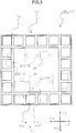
- Fig. 3 is a plan view of the electric circuit module 100 viewed from the bottom.
- Fig. 4 is a sectional view of the electric circuit module 100 viewed from an A-A line illustrated in Fig. 2 .
- Fig. 5 is a partially enlarged schematic drawing of the electric circuit module 100. It should be noted that Fig. 5 illustrates a state before an electric part 31 is sealed with resin.
- the electric circuit module 100 includes a rectangular multi-layer substrate 10 and a plurality of electric parts 31 that are mounted on the top layer 10a of the multi-layer substrate 10.
- the multi-layer substrate 10 is a multi-layer substrate with six layers including the top layer 10a, the bottom layer 10b, and four inner layers 10c.
- a wiring pattern 17 is formed in the top layer 10a and the inner layers 10c of the multi-layer substrate 10.
- An electric circuit 30 is formed by the wiring pattern 17 and a plurality of electric parts 31.
- the plurality of the electric parts 31 are sealed with sealing resin 35 that covers substantially all areas of the multi-layer substrate.
- the sealing resin 35 is made of thermosetting molding material in which the principal component is an epoxy resin and a silica filler, or the like, is added.
- the sealing resin 35 is used for protecting the electric parts 31 on the multi-layer substrate 10 from heat and moisture environments.
- a plurality of land electrodes 11 necessary for the normal operations are provided in the bottom layer 10b of the multi-layer substrate 10.
- the land electrodes 11 include a plurality of first land electrodes 11a and a single second land electrode 11b.
- the plurality of the first land electrodes 11a are used as, for example, a power supply terminal for supplying power to the electric circuit 30, an input terminal, an output terminal, and the like, of the electric circuit 30.
- the first land electrodes 11 are provided along the circumference of a surface of the bottom layer 10b of the multi-layer substrate 10.
- the second land electrode 11b is formed in the center of the bottom layer 10b of the multi-layer substrate 10.
- the second land electrode 11b has an area greater than the first land electrode 11a.
- the second land electrode 11b is used as a ground terminal of the electric circuit 30. It should be noted that the second land electrode 11b is formed by a single large land pattern. However, the second land electrode 11b may be formed by arranging a plurality of small land patterns.
- the plurality of the land electrodes 11, which are provided in the bottom layer 10b of the multi-layer substrate 10, are attached to an electric device such as a smart-phone in which the electric circuit module 100 is included, and thus, the electric circuit 30 is electrically connected to a circuit inside the electric device.
- the electric circuit module 100 includes test-use electrodes 13 that are used for identifying an electric part 31 that is a cause of an error when analyzing the error.
- the test-use electrodes 13 are provided in the multi-layer substrate on which the electric parts 31 are mounted.
- the test-use electrodes 13 are provided in the inner layers 10c of the multi-layer substrate 10. It should be noted that there are multiple test-use electrodes 13 included in the electric circuit module 100. Further, as it is not necessary to provide a test-use electrode that is used for checking the land electrodes 11 themselves for analyzing an error, the test-use electrodes 13 and the land electrodes 11 are not connected.
- test-use electrodes 13 are connected to the electric parts 31 that are error analysis targets, or to a point in the middle of the wiring pattern 17 that connects a plurality of the electric parts 31.
- a test-use electrode 13 is formed by a non-penetrating via hole 20 that is made of conductive material. Further, a connection land 20a of the non-penetrating via hole 20, which is formed in the top layer 10a of the multi-layer substrate 10, is connected to an electric part 31.
- the non-penetrating via hole 20 is not a via hole in which the layers in the multi-layer substrate are connected from the top layer 10a to the bottom layer 10b, but is a via hole which is formed from the top layer 10a or the bottom layer 10b to the inner layers 10c. In the electric circuit module 100, the non-penetrating via hole 20 is formed from the top layer 10a to the inner layers 10c.
- At least one of the plurality of the test-use electrodes 13 is a first test-use electrode 13a.
- a lower end surface of the first test-use electrode 13a is provided at one layer above the bottom layer 10b of the multi-layer substrate 10. Therefore, the test-use electrode 13 does not exist in an insulating layer 10d between the bottom layer 10b and a layer one layer above. Further, no wiring pattern 17 is provided in the bottom layer 10b of the multi-layer substrate 10.
- At least one of the plurality of the test-use electrode 13 is a second test-use electrode 13b.
- the second test-use electrode 13b is provided in the vicinity of a side end portion 10e of the multi-layer substrate 10. Further, no wiring pattern 17 is provided at least at a position, of the side end portion 10e of the multi-layer substrate 10, in the vicinity of the second test-use electrode 13b.
- a lower end surface 14 of the second test-use electrode 13b in the electric circuit module 100 is provided at one layer below the top layer 10a of the multi-layer substrate 10.
- the length of the second test-use electrode 13b is a length of a single layer of the insulating layer 10d.
- the non-penetrating via hole 20, which forms the test-use electrodes 13 is a stacked via hole 21 that is formed in a straight line in a direction perpendicular to the top layer 10a of the multi-layer substrate 10 (in a downward direction).
- the stacked via hole 21 is a via hole in which all of the vias formed in the inner layers 10c of the multi-layer substrate 10 are at the same position in a plan view.
- test-use electrodes 13 are formed in substantially a cylinder shape by extending from a connection land 20a in the top layer 10a toward the right downward direction (-Z direction). Therefore, as illustrated in Fig. 2 or Fig. 3 , when viewed from the top direction or the bottom direction in a plan view, the non-penetrating via holes 20 (i.e., the test-use electrodes 13) are formed in a circular shape.
- the stacked via holes 21 are used as the non-penetrating via holes 20 that form the test-use electrodes 13 in the electric circuit module 100.
- staggered vias whose upper and lower vias are not at the same position in a plan view, may also be used as the non-penetrating via holes 20.
- the stacked via holes 21 are formed, not by forming the stacked via holes 21 after the layers of the multi-layer substrate 10 have been layered, but by layering the layers, in which the via hole has already been formed, in the vertical direction.
- a resin is filled in an opening in the top layer 10a of the non-penetrating via hole 20, metal plating is applied to the resin, and the connection land 20a, which does not have a hole in the center, is formed on the top layer 10a of the multi-layer substrate 10. Further, a part pad 15 for the electric part 31 is provided in the top layer 10a, and the electric part 31 is attached to the part pad 15 via soldering, or the like.
- connection land 20a which is provided in the top layer 10a of the non-penetrating via hole 20, is used in common with the part pad 15.
- a pad on via 23 of the non-penetrating via hole 20 is formed in the top layer 10a of the multi-layer substrate 10. It is possible to improve the wiring space efficiency in the top layer 10a by forming the pad on via 23 in the top layer 10a of the multi-layer substrate 10.
- the wiring pattern 17, which is used for connecting the plurality of the electric parts 31 to each other or which is used for connecting the plurality of the electric parts 31 to the land electrodes 11, is provided in the top layer 10a and the inner layers 10c of the multi-layer substrate 10, but is not provided in the bottom layer 10b of the multi-layer substrate 10 as described above. Therefore, in the bottom layer 10b of the multi-layer substrate 10, nothing is formed other than the plurality of the land electrodes 11 (the first land electrodes 11a and the second land electrode 11b). Further, the test-use electrodes 13 are provided at positions at which the test-use electrodes 13 overlap the land electrodes 11 in a plan view.
- test-use electrodes 13, which are provided on the left side and the right side of the electric part 31 that is arranged on the right side in Fig. 4 are provided at positions at which the test-use electrodes 13 overlap the second land electrode 11b in a plan view. Further, the test-use electrodes 13, which are provided on the left side and the right side of the electric part 31 that is arranged on the left side in Fig. 4 , are provided at positions at which the test-use electrodes 13 overlap the first land electrode 11a or the second land electrode 11b in a plan view.
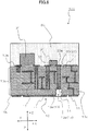
- Fig. 6 is a sectional view illustrating the first test method of the electric circuit module 100 viewed from A-A line in Fig. 2 .
- At least one of the test-use electrodes 13 is a first test-use electrode 13a.
- a ground part 19 is formed right under the first test-use electrode 13a, which is connected to the electric part 31, in the multi-layer substrate 10.
- the ground part 19 right under the first test-use electrode 13a is a drilled hole 19a.
- the drilled hole 19a can be formed by drilling the land electrode 11 and the insulating layer 10d that are formed on the bottom layer 10b.
- the first test method of the electric circuit module is a test method in which the first test-use electrode 13a is exposed by drilling the bottom layer 10b of the multi-layer substrate 10 at the time of analysis.
- a drill may be used for forming the drilled hole 19a, or, a laser beam may be applied to the bottom layer 10b of the multi-layer substrate 10 from the lower side (-Z side).
- a lower end surface 14 of the first test-use electrode 13a is exposed by forming the drilled hole 19a in the multi-layer substrate 10.
- the lower end surface 14 of the first test-use electrode 13a is provided at one layer above the bottom layer 10b of the multi-layer substrate 10, in order to expose the lower end surface 14, it is only necessary to drill a layer amount of the insulating layer 10d above the bottom layer 10b, and thus, preliminary work for performing analysis becomes easier.
- the lower end surface 14 of the first test-use electrode 13a is provided at one layer above the bottom layer 10b of the multi-layer substrate 10.
- the lower end surface 14 may be provided at a layer (position) other than the above-described layer (position).
- the first test-use electrode 13a is formed as the non-penetrating via hole 20 that has a thickness in the thickness direction of the multi-layer substrate 10, regardless of which layer the lower end surface 14 of the first test-use electrode 13a is provided in, and regardless of the drilling depth accuracy when drilling the insulating layer 10d of the multi-layer substrate 10, it is easy to expose the first test-use electrode 13a.
- the drilled hole 19a in the multi-layer substrate 10 After forming the drilled hole 19a in the multi-layer substrate 10, it is possible to perform checking, of the electric part 31 on the right side, for an error analysis by causing a probe for checking to be in contact with the lower end surface 14 of the first test-use electrode 13a.
- the same descriptions can be applied to first electrodes 13a for testing that are formed for other electric parts 31.
- the probe for checking is caused to be in contact with the lower end surface 14 of the first test-use electrode 13a through the drilled hole 19a formed in the bottom layer 10b of the multi-layer substrate 10, even if the electric part 31 is sealed with the sealing resin 35, it is not necessary to grind the sealing resin 35 in order to expose the first test-use electrode 13a.
- Fig. 7 is a sectional view illustrating the second test method of the electric circuit module 100 viewed from A-A line in Fig. 2 .
- the test-use electrodes 13 is a second test-use electrode 13b.
- a ground part 19 (drilled hole 19a) is formed right beside (right on the left side of) the test-use electrode 13 (i.e., the second test-use electrode 13b), which is connected to the left side of the electric part 31, in the multi-layer substrate 10.
- the second test method of the electric circuit module is a test method in which the second test-use electrode 13b is exposed by drilling the side end portion 10e of the multi-layer substrate 10 at the time of analysis.
- a side end portion surface of the second test-use electrode 13b is exposed by forming the drilled hole 19a in the multi-layer substrate 10.
- the second test-use electrode 13b is provided in the vicinity of the side end portion 10e of the multi-layer substrate 10. Therefore, it is only necessary to drill the insulating layer 10d of the side end portion 10e in the multi-layer substrate 10, and thus, preliminary work for performing analysis becomes easier.
- FIG. 8 is a sectional view of the electric circuit module 110 in the second test method (first modified example) viewed from A-A line in Fig. 2 .
- Fig. 9 is a partially enlarged schematic drawing of the electric circuit module 110 in the second test method (first modified example). It should be noted that Fig. 1 through Fig. 3 are common for the electric circuit module 100 and for the electric circuit module 110.
- the only difference between the electric circuit module 110 and the above-described electric circuit module 100 is that the length of the second test-use electrode 13c of the electric circuit module 110 is different from the length of the second test-use electrode 13b of the electric circuit module 100.
- the electric circuit module 110 is the same as the electric circuit module 100 other than the above difference. Therefore, the descriptions of the parts of the electric circuit module 110 that are the same as the electric circuit module 100 will be omitted.
- the second test-use electrode 13c is formed for the electric part 31 on the left side in Fig. 8 .
- the second test-use electrode 13c is provided in the vicinity of the side end portion 10e of the multi-layer substrate 10, and no wiring pattern 17 is provided at least at a position, of the side end portion 10e of the multi-layer substrate 10, in the vicinity of the second test-use electrode 13c.
- a lower end surface 14 of the second test-use electrode 13c in the electric circuit module 110 is provided at three layers below the top layer 10a of the multi-layer substrate 10.
- the length of the second test-use electrode 13c is a length of three layers of the insulating layer 10d. It should be noted that the length of the second test-use electrode 13c is not limited to the three layers amount as long as it has a length of multiple layers.
- a ground part 19 (drilled hole 19a) is formed right beside (right on the left side of) the test-use electrode 13 (i.e., the second test-use electrode 13c), which is connected to the left side of the electric part 31, in the side end portion 10e of the multi-layer substrate 10.
- the length of the second test-use electrode 13b is only an amount of one layer of the insulating layer 10d, and thus, it is very difficult to form the drilled hole 19a when the size of the electric circuit module 100 is small.
- the length of the second test-use electrode 13c is a length of multiple layers of the insulating layer 10d (length of three layers in Fig. 8 ), and thus, it is easier to form the drilled hole 19a even when the size of the electric circuit module 110 is small.
- the drilled hole 19a can be formed in the insulating layer 10d of the side end portion 10e in the multi-layer substrate 10 by using a drill, or the like. Further, in order to form the drilled hole 19a, laser light may be applied to the multi-layer substrate 10 from the left side (-X side).
- the second test-use electrode 13c has a length of an amount of multiple layers of the insulating layers 10d, and, by appropriately setting the length of the second test-use electrode 13c, it is possible to form a stub circuit such as an open stub and a short stub. As a result, by using the stub circuit, it becomes possible to form a filter circuit such as an impedance matching circuit and a trap circuit in the electric circuit 30.
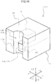
- FIG. 10 is a partially enlarged schematic drawing of the electric circuit module 110 in the second test method (second modified example).
- Fig. 11 is a partially enlarged schematic drawing of the electric circuit module 110 in the second test method (third modified example).
- the structure of the electric circuit module of the second test method (second modified example and third modified example) is the same as the structure of the electric circuit module 110 of the second test method (first modified example). Therefore, the descriptions of the structure of the electric circuit module 110 will be omitted.
- the second test method (second modified example) of the electric circuit module is a test method in which the ground part 19 is formed throughout the multi-layer substrate 10 and the sealing resin 35 of the electric circuit module 110.
- the above-described ground part 19 in the second test method (second modified example) is a partial ground part 19b.
- the partial ground part 19b is formed, for example, in a semicircle shape in a plan view by grinding the side end portion 10e of the multi-layer substrate 10 on the side on which the electric part 31 exists and by drilling a surface on the left side (a surface on -X side) of the sealing resin 35.
- the partial ground part 19b it is possible to expose the non-penetrating via hole 20 for testing the electric part 31 (i.e., the second test-use electrode 13c).
- the partial ground part 19b is not limited to be a semicircle shape in a plan view, and may be a rectangular shape in a plan view.
- the partial ground part 19b may be formed by using a file having a semicircle shape or a rectangular shape.
- the second test method (second modified example) of the electric circuit module even in the case where the size of the electric circuit module 110 is small, because of the fact that the partial ground part 19b is formed throughout (from the top to the bottom of) the outline of the left side (-X side) of the electric circuit module 110, compared with the second test method (first modified example) of the electric circuit module, it is easier to form the ground part 19 regardless of the position of the second test-use electrode 13c in the up-and-down direction.
- the second test method (third modified example) of the electric circuit module is a test method in which the ground part 19 is formed throughout the left side surface of the multi-layer substrate 10 and the sealing resin 35 of the electric circuit module 110.
- the above-described ground part 19 in the second test method (third modified example) is a total ground part 19c.
- the total ground part 19c is formed by grinding the entire surface on the left side (surface in -X side) of the side end portion 10e of the multi-layer substrate 10 and the sealing resin 35, and by having the left side surface of the multi-layer substrate 10 and the sealing resin 35 ground.
- the total ground part 19b it is possible to expose the non-penetrating via hole 20 for testing the electric part 31 (i.e., the second test-use electrode 13c).
- the total ground part 19c may be formed by using a file having a planar shape, or the like.
- the second test method (third modified example) of the electric circuit module even in the case where the size of the electric circuit module 110 is very small, because of the fact that the total ground part 19c is formed throughout the outline surface of the electric circuit module 110 on -X side, compared with the second test method (first modified example and second modified example) of the electric circuit module, it is further easier to form the ground part 19 regardless of the position of the second test-use electrode 13c in the Z direction and in the Y direction.
- the above-described electric circuit module includes the test-use electrodes used for an error analysis at a position, in an inner layer of the multi-layer substrate, at which the test-use electrodes overlap the land electrodes in a plan view. Therefore, it is not necessary for the electric circuit module to have an area that is used for exposing the test-use electrodes in the bottom layer of the multi-layer substrate. As a result, it is not necessary to increase an area of the bottom layer 10b of the multi-layer substrate 10, and thus, it becomes possible to reduce the size of the electric circuit module 100.
- the test-use electrodes 13 are formed by non-penetrating via holes 20, the test-use electrodes 13 have a thickness in the thickness direction of the multi-layer substrate 10, and have a thickness in the lateral direction of the multi-layer substrate 10. As a result, even when the accuracy of the grinding amount of the insulating layer 10d of the multi-layer substrate 10 is low, the test-use electrodes 13 can be still exposed easily.
- the lower end surface 14 of the first test-use electrode 13a is provided at one layer above the bottom layer 10b of the multi-layer substrate 10
- no wiring pattern 17 will be cut.
- the second test-use electrode 13b is provided in the vicinity of the side end portion 10e of the multi-layer substrate 10, when exposing the test-use electrode 13 used for an error analysis, it is only necessary to grind the side end portion 10e of the multi-layer substrate 10. Further, because of the fact that no wiring pattern 17 is provided at least at a position, of the side end portion 10e of the multi-layer substrate 10, in the vicinity of the second test-use electrode 13b, no wiring pattern 17 will be cut.
- the impact on the performance of the electric circuit module 100 can be reduced.
- connection lands 20a of the non-penetrating via holes 20 are used in common with the part pads 15 in the top layer 10a.
- sealing resin 35 Even though the electric parts 31 are sealed with sealing resin 35, it is not necessary to grind the sealing resin 35 in order to expose the test-use electrode 13.
- the lower end surface 14 of the first test-use electrode 13a is provided at one layer above the bottom layer 10b of the multi-layer substrate 10
- no wiring pattern 17 is provided in the bottom layer 10b of the multi-layer substrate 10, no wiring pattern 17 will be cut. Therefore, preliminary work for performing error analysis becomes easier.
- the second test-use electrode 13b is provided in the vicinity of the side end portion 10e of the multi-layer substrate 10 in the vicinity of the test-use electrode 13 used for an error analysis. Further, because of the fact that no wiring pattern 17 is provided at least at a position, of the side end portion 10e of the multi-layer substrate 10, in the vicinity of the second test-use electrode 13b, no wiring pattern 17 will be cut. Therefore, preliminary work for performing error analysis becomes easier.
- test-use electrodes used for an error analysis are provided at a position, in an inner layer of the multi-layer substrate, at which the test-use electrodes overlap the land electrodes in a plan view, it is not necessary to have an area that is used for exposing the test-use electrodes in the bottom layer of the multi-layer substrate. As a result, it is not necessary to increase an area of the bottom layer of the multi-layer substrate, and thus, it becomes possible to reduce the size of the electric circuit module.
- the first test method of the electric circuit module because of the fact that the lower end surface of the first test-use electrode is provided at one layer above the bottom layer of the multi-layer substrate, it is only necessary to grind the insulating layer of the bottom layer of the multi-layer substrate when exposing the test-use electrode used for an error analysis. Further, because of the fact that no wiring pattern is provided in the bottom layer of the multi-layer substrate, no wiring pattern will be cut. Therefore, preliminary work for performing error analysis becomes easier. Further, in the second test method of the electric circuit module, because of the fact that the second test-use electrode is provided in the vicinity of the side end portion of the multi-layer substrate, it is only necessary to grind the side end portion of the multi-layer substrate when exposing the test-use electrode used for an error analysis. Further, because of the fact that no wiring pattern is provided at least at a position, of the side end portion of the multi-layer substrate, in the vicinity of the second test-use electrode, no wiring pattern will be cut. Therefore, preliminary work for performing error analysis becomes easier.
Landscapes
- Engineering & Computer Science (AREA)
- Microelectronics & Electronic Packaging (AREA)
- Manufacturing & Machinery (AREA)
- Printing Elements For Providing Electric Connections Between Printed Circuits (AREA)
- Production Of Multi-Layered Print Wiring Board (AREA)
Abstract
Description
- The present invention relates to an electric circuit module, and, in particular, relates to an electric circuit module that includes a test-use electrode, and relates to a test method of the electric circuit module.
- In recent years, electric circuit modules that include a test-use electrode have been developed. The test-use electrode is included for identifying an electric part that causes an error at the time of error analysis. For example, in the case where electric parts are covered with sealing resin, test probes cannot be directly in contact with the electric parts. A plurality of test-use electrodes, which are connected to the electric parts through via-holes, are included in the bottom layer of a multi-layer substrate on which the electric parts are mounted. Conductivity checks, etc., are performed by causing the test probes to be in contact with the test-use electrodes.
- However, as a result of the plurality of the test-use electrodes that must be included in the bottom layer of the multi-layer substrate in addition to a plurality of land electrodes that are necessary for operating the electric circuit module, an area of the multi-layer substrate is inevitably increased, which has caused the size of the electric circuit module to increase. Therefore, an electric circuit module that is not required to include a test-use electrode in the bottom layer of the multi-layer substrate has been developed. As this kind of the electric circuit module, a multi-layer printed
wiring board 900 is disclosed inPatent Document 1. In the following, referring toFig. 12 , the multi-layer printedwiring board 900 will be described. - In the multi-layer printed
wiring board 900, in order to execute a continuity check between circuits of layers before placing electronic components or an input/output functional test between the circuits of the layers after placing the electric components,copper foils 904 of predetermined portions of one surface or both surfaces of a substrate 301 are removed by etching, aninsulating layer 902 exposed at the portions is removed by dissolving it in alkaline water solution to exposelands check lands lands - According to the arrangements described above, the check lands for checking electrical connection between the circuits of the layers or for testing functions can be formed by using the lands of the inner layer circuit.
- [Patent Document 1] Japanese Unexamined Patent Application Publication No.
H07-007272 - However, in the multi-layer printed
wiring board 900, an area that is used for exposing thecheck lands substrate 901. Further, when some parts of the electric circuits including a wiring pattern, etc., are provided in the top layer and the bottom layer, it is necessary to avoid the area in which those parts are provided to expose thecheck lands substrate 901 larger than the conventional area. As a result, there is a problem that it is difficult to make the size of the electric circuit module smaller. - In view of the above-described problem of conventional technologies, the present invention provides an electric circuit module that includes a test-use electrode in an inner layer of a multi-layer substrate and whose size is easy to be made smaller, and provides a test method of the electric circuit module in which preliminary work for performing error analysis becomes easy.
- In order to solve the above-described problem, an electric circuit module according to an embodiment of the present invention includes a multi-layer substrate, and a plurality of electric parts mounted on a top layer of the multi-layer substrate, and has the features that a plurality of land electrodes that are necessary for normal operations are provided in a bottom layer of the multi-layer substrate, that test-use electrodes connected to the electric parts are provided in an inner layer of the multi-layer substrate, that the test-use electrodes are not connected to the land electrodes, and that the test-use electrodes are provided at a position at which the test-use electrodes overlap the land electrodes in a plan view.
- The above-described electric circuit module includes the test-use electrodes used for an error analysis at a position, in an inner layer of the multi-layer substrate, at which the test-use electrodes overlap the land electrodes in a plan view. Therefore, it is not necessary for the electric circuit module to have an area that is used for exposing the test-use electrodes in the bottom layer of the multi-layer substrate. As a result, it is not necessary to increase an area of the bottom layer of the multi-layer substrate, and thus, it becomes possible to reduce the size of the electric circuit module.
- Furthermore, in the above-described arrangement, the electric circuit module has the features that the test-use electrodes are formed by non-penetrating via-holes made of conductive material.
- In the above-described electric circuit module, because the test-use electrodes are formed by non-penetrating via holes, the test-use electrodes have a thickness in the thickness direction of the multi-layer substrate, and have a thickness in the lateral direction of the multi-layer substrate. As a result, even when the accuracy of the grinding amount of an insulating layer of the multi-layer substrate is low, the test-use electrodes can be still exposed easily.
- Further, the above-described electric circuit module has the features that at least one of the test-use electrodes is a first test-use electrode whose lower end surface is provided at one layer above the bottom layer of the multi-layer substrate, and that no wiring pattern is provided in the bottom layer of the multi-layer substrate.
- In the above-described electric circuit module, because of the fact that the lower end surface of the first test-use electrode is provided at one layer above the bottom layer of the multi-layer substrate, when exposing the test-use electrode used for an error analysis, it is only necessary to grind the insulating layer of the bottom layer of the multi-layer substrate. Further, because of the fact that no wiring pattern is provided in the bottom layer of the multi-layer substrate, no wiring pattern will be cut.
- Further, in the above-described case, at least one of the test-use electrodes is a second test-use electrode that is provided in the vicinity of the side end portion of the multi-layer substrate, and no wiring pattern is provided at least at a position, of the side end portion of the multi-layer substrate, in the vicinity of the second test-use electrode.
- In the above-described electric circuit module, because of the fact that the second test-use electrode is provided in the vicinity of the side end portion of the multi-layer substrate, when exposing the test-use electrode used for an error analysis, it is only necessary to grind the side end portion of the multi-layer substrate. Further, because of the fact that no wiring pattern is provided at least at a position, of the side end portion of the multi-layer substrate, in the vicinity of the second test-use electrode, no wiring pattern will be cut.
- Further, in the above-described case, the non-penetrating via holes are stacked via holes that are formed in a straight line in a direction perpendicular to the top layer of the multi-layer substrate.
- In the above-described electric circuit module, it is possible to cause the non-penetrating via holes that form the test-use electrode to have a minimum required length, and thus, the impact on the performance of the electric circuit module can be reduced.
- Further, the above-described electric circuit module has the features that part pads for the electric parts are provided in the top layer of the multi-layer substrate, and that connection lands of the non-penetrating via holes on the top layer are used in common with the part pads.
- In the above-described electric circuit module, it is possible to improve the wiring space efficiency by a pad-on-via in which the connection lands of the non-penetrating via holes in the top layer are used in common with the part pads.
- Further, the above-described electric circuit module has the features that the electric parts are sealed with resin.
- In the above-described electric circuit module, even though the electric parts are sealed with resin, it is not necessary to grind the sealing resin in order to expose the test-use electrode.
- In order to solve the above-described problem, a first test method of an electric circuit module according to an embodiment of the present invention is a test method of an electric circuit module that includes a multi-layer substrate and a plurality of electric parts mounted on a top layer of the multi-layer substrate, wherein a plurality of land electrodes necessary for ordinary operations are provided in a bottom layer of the multi-layer substrate, and test-use electrodes connected to the electric parts are provided in an inner layer of the multi-layer substrate. The method includes providing the test-use electrodes at a position at which the test-use electrodes overlaps the land electrodes in a plan view, causing at least one of the test-use electrode to be a first test-use electrode whose lower end surface is provided at one layer above the bottom layer of the multi-layer substrate, not connecting the first test-use electrode to the land electrode, not providing a wiring pattern in the bottom layer of the multi-layer substrate, and exposing the first test-use electrode by grinding the bottom layer of the multi-layer substrate at the time of analysis.
- In the above-described first test method of the electric circuit module, because of the fact that the lower end surface of the first test-use electrode is provided at one layer above the bottom layer of the multi-layer substrate, when exposing the test-use electrode used for an error analysis, it is only necessary to grind the insulating layer of the bottom layer of the multi-layer substrate. Further, because of the fact that no wiring pattern is provided in the bottom layer of the multi-layer substrate, no wiring pattern will be cut. Therefore, preliminary work for performing error analysis becomes easier.
- In order to solve the above-described problem, a second test method of an electric circuit module according to an embodiment of the present invention is a test method of an electric circuit module that includes a multi-layer substrate and a plurality of electric parts mounted on a top layer of the multi-layer substrate, wherein a plurality of land electrodes necessary for ordinary operations are provided in a bottom layer of the multi-layer substrate, and test-use electrodes connected to the electric parts are provided in an inner layer of the multi-layer substrate. The method includes providing the test-use electrodes at a position at which the test-use electrodes overlaps the land electrodes in a plan view, causing at least one of the test-use electrode to be a second test-use electrode provided in the vicinity of the side end portion of the multi-layer substrate, not connecting the second test-use electrode to the land electrode, not providing a wiring pattern at least at a position, of the side end portion of the multi-layer substrate, in the vicinity of the second test-use electrode, and exposing the second test-use electrode by grinding the side end portion of the multi-layer substrate at the time of analysis.
- In the above-described second test method of the electric circuit module, because of the fact that the second test-use electrode is provided in the vicinity of the side end portion of the multi-layer substrate, when exposing the test-use electrode used for an error analysis, it is only necessary to grind the side end portion of the multi-layer substrate. Further, because of the fact that no wiring pattern is provided at least at a position, of the side end portion of the multi-layer substrate, in the vicinity of the second test-use electrode, no wiring pattern will be cut. Therefore, preliminary work for performing error analysis becomes easier.
- An electric circuit module according to an embodiment of the present invention includes the test-use electrodes used for an error analysis at a position, in an inner layer of the multi-layer substrate, at which the test-use electrodes overlap the land electrodes in a plan view. Therefore, it is not necessary for the electric circuit module to have an area that is used for exposing the test-use electrodes in the bottom layer of the multi-layer substrate. As a result, it is not necessary to increase an area of the bottom layer of the multi-layer substrate, and thus, it becomes possible to reduce the size of the electric circuit module. Further, in the above-described first test method of the electric circuit module, because of the fact that the lower end surface of the first test-use electrode is provided at one layer above the bottom layer of the multi-layer substrate, when exposing the test-use electrode used for an error analysis, it is only necessary to grind the insulating layer of the bottom layer of the multi-layer substrate. Further, because of the fact that no wiring pattern is provided in the bottom layer of the multi-layer substrate, no wiring pattern will be cut. Therefore, preliminary work for performing error analysis becomes easier. Further, in the above-described second test method of the electric circuit module, because of the fact that the second test-use electrode is provided in the vicinity of the side end portion of the multi-layer substrate, when exposing the test-use electrode used for an error analysis, it is only necessary to grind the side end portion of the multi-layer substrate. Further, because of the fact that no wiring pattern is provided at least at a position, of the side end portion of the multi-layer substrate, in the vicinity of the second test-use electrode, no wiring pattern will be cut. Therefore, preliminary work for performing error analysis becomes easier.
-
-
Fig. 1 is a perspective view illustrating an appearance of an electric circuit module according to an embodiment of the present invention. -
Fig. 2 is a plan view of the electric circuit module viewed from the top. -
Fig. 3 is a plan view of the electric circuit module viewed from the bottom. -
Fig. 4 is a sectional view of the electric circuit module. -
Fig. 5 is a partially enlarged schematic drawing of the electric circuit module. -
Fig. 6 is a sectional view illustrating a first test method of the electric circuit module. -
Fig. 7 is a sectional view illustrating a second test method of the electric circuit module. -
Fig. 8 is a sectional view illustrating a first modified example of the second test method. -
Fig. 9 is a partially enlarged schematic drawing illustrating a first modified example of the second test method. -
Fig. 10 is a partially enlarged schematic drawing illustrating a second modified example of the second test method. -
Fig. 11 is a partially enlarged schematic drawing illustrating a third modified example of the second test method. -
Fig. 12 is a sectional view of a multi-layer printed wiring board according to a conventional example. - In the following, referring to the drawings, an electric circuit module and a test method of the electric circuit module according to an embodiment of the present invention will be described. An electric circuit module according to an embodiment of the present invention is, for example, a small electric circuit module that includes a high-frequency circuit used for a wireless LAN (Local Area Network), Bluetooth (registered trademark), etc., and that is mounted on an electric device such as a smart-phone. The use of the electric circuit module according to an embodiment of the present invention is not limited to an embodiment described below, and various modifications may be made. It should be noted that, in the case where "right side", "left side", "upper side", and "lower side" are used in the descriptions for the drawings, they indicate "+X side", "-X side", "+Z side", and "-Z side", respectively, in each of the drawings.
- First, referring to
Fig. 1 through Fig. 5 , a structure of anelectric circuit module 100 according to an embodiment of the present invention will be described.Fig. 1 is a perspective view illustrating an appearance of theelectric circuit module 100.Fig. 2 is a plan view of theelectric circuit module 100 viewed from the top.Fig. 3 is a plan view of theelectric circuit module 100 viewed from the bottom. Further,Fig. 4 is a sectional view of theelectric circuit module 100 viewed from an A-A line illustrated inFig. 2 .Fig. 5 is a partially enlarged schematic drawing of theelectric circuit module 100. It should be noted thatFig. 5 illustrates a state before anelectric part 31 is sealed with resin. - As illustrated in
Fig. 1 andFig. 2 , theelectric circuit module 100 includes a rectangularmulti-layer substrate 10 and a plurality ofelectric parts 31 that are mounted on thetop layer 10a of themulti-layer substrate 10. As illustrated inFig. 4 , themulti-layer substrate 10 is a multi-layer substrate with six layers including thetop layer 10a, the bottom layer 10b, and fourinner layers 10c. Awiring pattern 17 is formed in thetop layer 10a and theinner layers 10c of themulti-layer substrate 10. Anelectric circuit 30 is formed by thewiring pattern 17 and a plurality ofelectric parts 31. - The plurality of the
electric parts 31 are sealed with sealingresin 35 that covers substantially all areas of the multi-layer substrate. The sealingresin 35 is made of thermosetting molding material in which the principal component is an epoxy resin and a silica filler, or the like, is added. The sealingresin 35 is used for protecting theelectric parts 31 on themulti-layer substrate 10 from heat and moisture environments. - As illustrated in
Fig. 3 , a plurality ofland electrodes 11 necessary for the normal operations are provided in the bottom layer 10b of themulti-layer substrate 10. Theland electrodes 11 include a plurality offirst land electrodes 11a and a singlesecond land electrode 11b. The plurality of thefirst land electrodes 11a are used as, for example, a power supply terminal for supplying power to theelectric circuit 30, an input terminal, an output terminal, and the like, of theelectric circuit 30. In theelectric circuit module 100, thefirst land electrodes 11 are provided along the circumference of a surface of the bottom layer 10b of themulti-layer substrate 10. - The
second land electrode 11b is formed in the center of the bottom layer 10b of themulti-layer substrate 10. Thesecond land electrode 11b has an area greater than thefirst land electrode 11a. Thesecond land electrode 11b is used as a ground terminal of theelectric circuit 30. It should be noted that thesecond land electrode 11b is formed by a single large land pattern. However, thesecond land electrode 11b may be formed by arranging a plurality of small land patterns. - The plurality of the
land electrodes 11, which are provided in the bottom layer 10b of themulti-layer substrate 10, are attached to an electric device such as a smart-phone in which theelectric circuit module 100 is included, and thus, theelectric circuit 30 is electrically connected to a circuit inside the electric device. - The
electric circuit module 100 includes test-use electrodes 13 that are used for identifying anelectric part 31 that is a cause of an error when analyzing the error. In case of theelectric circuit module 100, because of the fact that theelectric parts 31 are covered with the sealingresin 35, a test probe cannot be directly in contact with a terminal included in theelectric parts 31. Therefore, it is necessary that the test-use electrodes 13 be provided in the multi-layer substrate on which theelectric parts 31 are mounted. As illustrated inFig. 4 , in theelectric circuit module 100, the test-use electrodes 13 are provided in theinner layers 10c of themulti-layer substrate 10. It should be noted that there are multiple test-use electrodes 13 included in theelectric circuit module 100. Further, as it is not necessary to provide a test-use electrode that is used for checking theland electrodes 11 themselves for analyzing an error, the test-use electrodes 13 and theland electrodes 11 are not connected. - The test-
use electrodes 13 are connected to theelectric parts 31 that are error analysis targets, or to a point in the middle of thewiring pattern 17 that connects a plurality of theelectric parts 31. As illustrated inFig. 4 , a test-use electrode 13 is formed by a non-penetrating viahole 20 that is made of conductive material. Further, aconnection land 20a of the non-penetrating viahole 20, which is formed in thetop layer 10a of themulti-layer substrate 10, is connected to anelectric part 31. - The non-penetrating via
hole 20 is not a via hole in which the layers in the multi-layer substrate are connected from thetop layer 10a to the bottom layer 10b, but is a via hole which is formed from thetop layer 10a or the bottom layer 10b to theinner layers 10c. In theelectric circuit module 100, the non-penetrating viahole 20 is formed from thetop layer 10a to theinner layers 10c. - At least one of the plurality of the test-
use electrodes 13 is a first test-use electrode 13a. A lower end surface of the first test-use electrode 13a is provided at one layer above the bottom layer 10b of themulti-layer substrate 10. Therefore, the test-use electrode 13 does not exist in an insulatinglayer 10d between the bottom layer 10b and a layer one layer above. Further, nowiring pattern 17 is provided in the bottom layer 10b of themulti-layer substrate 10. - Further, at least one of the plurality of the test-
use electrode 13 is a second test-use electrode 13b. The second test-use electrode 13b is provided in the vicinity of aside end portion 10e of themulti-layer substrate 10. Further, nowiring pattern 17 is provided at least at a position, of theside end portion 10e of themulti-layer substrate 10, in the vicinity of the second test-use electrode 13b. It should be noted that alower end surface 14 of the second test-use electrode 13b in theelectric circuit module 100 is provided at one layer below thetop layer 10a of themulti-layer substrate 10. In other words, the length of the second test-use electrode 13b is a length of a single layer of the insulatinglayer 10d. - In the
electric circuit module 100, the non-penetrating viahole 20, which forms the test-use electrodes 13, is a stacked viahole 21 that is formed in a straight line in a direction perpendicular to thetop layer 10a of the multi-layer substrate 10 (in a downward direction). The stacked viahole 21 is a via hole in which all of the vias formed in theinner layers 10c of themulti-layer substrate 10 are at the same position in a plan view. - Therefore, the test-use electrodes 13 (the first test-
use electrode 13a and the second test-use electrode 13b) are formed in substantially a cylinder shape by extending from aconnection land 20a in thetop layer 10a toward the right downward direction (-Z direction). Therefore, as illustrated inFig. 2 orFig. 3 , when viewed from the top direction or the bottom direction in a plan view, the non-penetrating via holes 20 (i.e., the test-use electrodes 13) are formed in a circular shape. - It is possible to cause the length of the non-penetrating via
holes 20, which form the test-use electrodes 13, to be a minimum required length, and thus, the impact on the performance of the electric circuit module can be reduced. - It should be noted that the stacked via
holes 21 are used as the non-penetrating viaholes 20 that form the test-use electrodes 13 in theelectric circuit module 100. However, staggered vias, whose upper and lower vias are not at the same position in a plan view, may also be used as the non-penetrating via holes 20. Further, in theelectric circuit module 100, when forming the stacked viaholes 21 in themulti-layer substrate 10, the stacked viaholes 21 are formed, not by forming the stacked viaholes 21 after the layers of themulti-layer substrate 10 have been layered, but by layering the layers, in which the via hole has already been formed, in the vertical direction. - As illustrated in
Fig. 5 , a resin is filled in an opening in thetop layer 10a of the non-penetrating viahole 20, metal plating is applied to the resin, and theconnection land 20a, which does not have a hole in the center, is formed on thetop layer 10a of themulti-layer substrate 10. Further, apart pad 15 for theelectric part 31 is provided in thetop layer 10a, and theelectric part 31 is attached to thepart pad 15 via soldering, or the like. - In the
electric circuit module 100, theconnection land 20a, which is provided in thetop layer 10a of the non-penetrating viahole 20, is used in common with thepart pad 15. In other words, a pad on via 23 of the non-penetrating viahole 20 is formed in thetop layer 10a of themulti-layer substrate 10. It is possible to improve the wiring space efficiency in thetop layer 10a by forming the pad on via 23 in thetop layer 10a of themulti-layer substrate 10. - Further, as illustrated in
Fig. 4 , thewiring pattern 17, which is used for connecting the plurality of theelectric parts 31 to each other or which is used for connecting the plurality of theelectric parts 31 to theland electrodes 11, is provided in thetop layer 10a and theinner layers 10c of themulti-layer substrate 10, but is not provided in the bottom layer 10b of themulti-layer substrate 10 as described above. Therefore, in the bottom layer 10b of themulti-layer substrate 10, nothing is formed other than the plurality of the land electrodes 11 (thefirst land electrodes 11a and thesecond land electrode 11b). Further, the test-use electrodes 13 are provided at positions at which the test-use electrodes 13 overlap theland electrodes 11 in a plan view. - For example, the test-
use electrodes 13, which are provided on the left side and the right side of theelectric part 31 that is arranged on the right side inFig. 4 , are provided at positions at which the test-use electrodes 13 overlap thesecond land electrode 11b in a plan view. Further, the test-use electrodes 13, which are provided on the left side and the right side of theelectric part 31 that is arranged on the left side inFig. 4 , are provided at positions at which the test-use electrodes 13 overlap thefirst land electrode 11a or thesecond land electrode 11b in a plan view. - Next, referring to
Fig. 6 , a state of theelectric circuit module 100 in a first test method of an electric circuit module according to an embodiment of the present invention, that is, a state of theelectric circuit module 100 at the time of preliminary work for performing error analysis, will be described.Fig. 6 is a sectional view illustrating the first test method of theelectric circuit module 100 viewed from A-A line inFig. 2 . - As illustrated in
Fig. 6 , at least one of the test-use electrodes 13 is a first test-use electrode 13a. In the first test method of the electric circuit module, in case of performing an error analysis of theelectric circuit module 100, for example, in case of performing an error analysis of anelectric part 31 on the right side inFig. 6 , aground part 19 is formed right under the first test-use electrode 13a, which is connected to theelectric part 31, in themulti-layer substrate 10. Theground part 19 right under the first test-use electrode 13a is a drilledhole 19a. The drilledhole 19a can be formed by drilling theland electrode 11 and the insulatinglayer 10d that are formed on the bottom layer 10b. - In other words, the first test method of the electric circuit module is a test method in which the first test-
use electrode 13a is exposed by drilling the bottom layer 10b of themulti-layer substrate 10 at the time of analysis. It should be noted that a drill may be used for forming the drilledhole 19a, or, a laser beam may be applied to the bottom layer 10b of themulti-layer substrate 10 from the lower side (-Z side). - A
lower end surface 14 of the first test-use electrode 13a is exposed by forming the drilledhole 19a in themulti-layer substrate 10. As described above, because of the fact that thelower end surface 14 of the first test-use electrode 13a is provided at one layer above the bottom layer 10b of themulti-layer substrate 10, in order to expose thelower end surface 14, it is only necessary to drill a layer amount of the insulatinglayer 10d above the bottom layer 10b, and thus, preliminary work for performing analysis becomes easier. - It should be noted that, in order to expose the
lower end surface 14 of the test-use electrode 13, not only the bottom layer 10b and the insulatinglayer 10d right under thelower end surface 14 of the first test-use electrode 13a may be drilled, but also all of the bottom layer 10b of themulti-layer substrate 10 and all of a layer amount of the insulatinglayer 10d above the bottom layer 10b may be drilled. - Further, in the
electric circuit module 100, thelower end surface 14 of the first test-use electrode 13a is provided at one layer above the bottom layer 10b of themulti-layer substrate 10. However, thelower end surface 14 may be provided at a layer (position) other than the above-described layer (position). Further, as described above, because of the fact that the first test-use electrode 13a is formed as the non-penetrating viahole 20 that has a thickness in the thickness direction of themulti-layer substrate 10, regardless of which layer thelower end surface 14 of the first test-use electrode 13a is provided in, and regardless of the drilling depth accuracy when drilling the insulatinglayer 10d of themulti-layer substrate 10, it is easy to expose the first test-use electrode 13a. - Further, because of the fact that no
wiring pattern 17 is formed in the bottom layer 10b of themulti-layer substrate 10, nowiring pattern 17 will be cut when forming the ground part 19 (drilledhole 19a) in themulti-layer substrate 10. Therefore, at the time of an error analysis, no impact will be made on the result. - After forming the drilled
hole 19a in themulti-layer substrate 10, it is possible to perform checking, of theelectric part 31 on the right side, for an error analysis by causing a probe for checking to be in contact with thelower end surface 14 of the first test-use electrode 13a. The same descriptions can be applied tofirst electrodes 13a for testing that are formed for otherelectric parts 31. In this way, because of the fact that the probe for checking is caused to be in contact with thelower end surface 14 of the first test-use electrode 13a through the drilledhole 19a formed in the bottom layer 10b of themulti-layer substrate 10, even if theelectric part 31 is sealed with the sealingresin 35, it is not necessary to grind the sealingresin 35 in order to expose the first test-use electrode 13a. - Next, referring to
Fig. 7 , a state of theelectric circuit module 100 in a second test method of an electric circuit module according to an embodiment of the present invention, that is, a state of theelectric circuit module 100 at the time of preliminary work for performing error analysis, will be described.Fig. 7 is a sectional view illustrating the second test method of theelectric circuit module 100 viewed from A-A line inFig. 2 . - As illustrated in
Fig. 7 , at least one of the test-use electrodes 13 is a second test-use electrode 13b. For example, in case of performing an error analysis of anelectric part 31 on the left side inFig. 7 , a ground part 19 (drilledhole 19a) is formed right beside (right on the left side of) the test-use electrode 13 (i.e., the second test-use electrode 13b), which is connected to the left side of theelectric part 31, in themulti-layer substrate 10. In other words, the second test method of the electric circuit module is a test method in which the second test-use electrode 13b is exposed by drilling theside end portion 10e of themulti-layer substrate 10 at the time of analysis. - A side end portion surface of the second test-
use electrode 13b is exposed by forming the drilledhole 19a in themulti-layer substrate 10. As described above, the second test-use electrode 13b is provided in the vicinity of theside end portion 10e of themulti-layer substrate 10. Therefore, it is only necessary to drill the insulatinglayer 10d of theside end portion 10e in themulti-layer substrate 10, and thus, preliminary work for performing analysis becomes easier. - Further, because of the fact that no
wiring pattern 17 is provided at least at a position, of theside end portion 10e of themulti-layer substrate 10, in the vicinity of the second test-use electrode 13b, no wiring pattern will be cut when forming the drilledhole 19a in themulti-layer substrate 10. Therefore, at the time of an error analysis, no impact will be made on the result. - After forming the drilled
hole 19a, which extends to the ground part 19 (drilledhole 19a), in themulti-layer substrate 10, it is possible to perform checking, of theelectric part 31 on the left side inFig. 7 , for an error analysis by causing a probe for checking to be in contact with the left side surface of the second test-use electrode 13b. - Next, referring to
Fig. 8 andFig. 9 , a state of anelectric circuit module 110 in the second test method of anelectric circuit module 110 according to an embodiment of the present invention, that is, a state of theelectric circuit module 110 at the time of preliminary work for performing error analysis, will be described.Fig. 8 is a sectional view of theelectric circuit module 110 in the second test method (first modified example) viewed from A-A line inFig. 2 .Fig. 9 is a partially enlarged schematic drawing of theelectric circuit module 110 in the second test method (first modified example). It should be noted thatFig. 1 through Fig. 3 are common for theelectric circuit module 100 and for theelectric circuit module 110. - The only difference between the
electric circuit module 110 and the above-describedelectric circuit module 100 is that the length of the second test-use electrode 13c of theelectric circuit module 110 is different from the length of the second test-use electrode 13b of theelectric circuit module 100. Theelectric circuit module 110 is the same as theelectric circuit module 100 other than the above difference. Therefore, the descriptions of the parts of theelectric circuit module 110 that are the same as theelectric circuit module 100 will be omitted. - As illustrated in
Fig. 8 andFig. 9 , in theelectric circuit module 110, the second test-use electrode 13c is formed for theelectric part 31 on the left side inFig. 8 . The second test-use electrode 13c is provided in the vicinity of theside end portion 10e of themulti-layer substrate 10, and nowiring pattern 17 is provided at least at a position, of theside end portion 10e of themulti-layer substrate 10, in the vicinity of the second test-use electrode 13c. As illustrated inFig. 8 , alower end surface 14 of the second test-use electrode 13c in theelectric circuit module 110 is provided at three layers below thetop layer 10a of themulti-layer substrate 10. In other words, the length of the second test-use electrode 13c is a length of three layers of the insulatinglayer 10d. It should be noted that the length of the second test-use electrode 13c is not limited to the three layers amount as long as it has a length of multiple layers. - In case of performing an error analysis of an
electric part 31 of theelectric circuit module 110 on the left side inFig. 8 , similar to the case of theelectric circuit module 100, as illustrated inFig. 8 andFig. 9 , a ground part 19 (drilledhole 19a) is formed right beside (right on the left side of) the test-use electrode 13 (i.e., the second test-use electrode 13c), which is connected to the left side of theelectric part 31, in theside end portion 10e of themulti-layer substrate 10. - In case of the
electric circuit module 100, the length of the second test-use electrode 13b is only an amount of one layer of the insulatinglayer 10d, and thus, it is very difficult to form the drilledhole 19a when the size of theelectric circuit module 100 is small. In case of theelectric circuit module 110, however, the length of the second test-use electrode 13c is a length of multiple layers of the insulatinglayer 10d (length of three layers inFig. 8 ), and thus, it is easier to form the drilledhole 19a even when the size of theelectric circuit module 110 is small. - The drilled
hole 19a can be formed in the insulatinglayer 10d of theside end portion 10e in themulti-layer substrate 10 by using a drill, or the like. Further, in order to form the drilledhole 19a, laser light may be applied to themulti-layer substrate 10 from the left side (-X side). - It should be noted that the second test-
use electrode 13c has a length of an amount of multiple layers of the insulatinglayers 10d, and, by appropriately setting the length of the second test-use electrode 13c, it is possible to form a stub circuit such as an open stub and a short stub. As a result, by using the stub circuit, it becomes possible to form a filter circuit such as an impedance matching circuit and a trap circuit in theelectric circuit 30. - Next, referring to
Fig. 10 andFig. 11 , a state of anelectric circuit module 110 in the second test method (second modified example, third modified example) of anelectric circuit module 110 according to an embodiment of the present invention, that is, a state of theelectric circuit module 110 at the time of preliminary work for performing error analysis, will be described.Fig. 10 is a partially enlarged schematic drawing of theelectric circuit module 110 in the second test method (second modified example).Fig. 11 is a partially enlarged schematic drawing of theelectric circuit module 110 in the second test method (third modified example). - The structure of the electric circuit module of the second test method (second modified example and third modified example) is the same as the structure of the
electric circuit module 110 of the second test method (first modified example). Therefore, the descriptions of the structure of theelectric circuit module 110 will be omitted. - As illustrated in
Fig. 10 , the second test method (second modified example) of the electric circuit module is a test method in which theground part 19 is formed throughout themulti-layer substrate 10 and the sealingresin 35 of theelectric circuit module 110. The above-describedground part 19 in the second test method (second modified example) is apartial ground part 19b. - The
partial ground part 19b is formed, for example, in a semicircle shape in a plan view by grinding theside end portion 10e of themulti-layer substrate 10 on the side on which theelectric part 31 exists and by drilling a surface on the left side (a surface on -X side) of the sealingresin 35. By forming thepartial ground part 19b, it is possible to expose the non-penetrating viahole 20 for testing the electric part 31 (i.e., the second test-use electrode 13c).
It should be noted that thepartial ground part 19b is not limited to be a semicircle shape in a plan view, and may be a rectangular shape in a plan view. Thepartial ground part 19b may be formed by using a file having a semicircle shape or a rectangular shape. - In the second test method (second modified example) of the electric circuit module, even in the case where the size of the
electric circuit module 110 is small, because of the fact that thepartial ground part 19b is formed throughout (from the top to the bottom of) the outline of the left side (-X side) of theelectric circuit module 110, compared with the second test method (first modified example) of the electric circuit module, it is easier to form theground part 19 regardless of the position of the second test-use electrode 13c in the up-and-down direction. - As illustrated in
Fig. 11 , the second test method (third modified example) of the electric circuit module is a test method in which theground part 19 is formed throughout the left side surface of themulti-layer substrate 10 and the sealingresin 35 of theelectric circuit module 110. The above-describedground part 19 in the second test method (third modified example) is atotal ground part 19c. - The
total ground part 19c is formed by grinding the entire surface on the left side (surface in -X side) of theside end portion 10e of themulti-layer substrate 10 and the sealingresin 35, and by having the left side surface of themulti-layer substrate 10 and the sealingresin 35 ground. By forming thetotal ground part 19b, it is possible to expose the non-penetrating viahole 20 for testing the electric part 31 (i.e., the second test-use electrode 13c). Thetotal ground part 19c may be formed by using a file having a planar shape, or the like. - In the second test method (third modified example) of the electric circuit module, even in the case where the size of the
electric circuit module 110 is very small, because of the fact that thetotal ground part 19c is formed throughout the outline surface of theelectric circuit module 110 on -X side, compared with the second test method (first modified example and second modified example) of the electric circuit module, it is further easier to form theground part 19 regardless of the position of the second test-use electrode 13c in the Z direction and in the Y direction. - In the following, effects according to an embodiment of the present invention will be described.
- The above-described electric circuit module includes the test-use electrodes used for an error analysis at a position, in an inner layer of the multi-layer substrate, at which the test-use electrodes overlap the land electrodes in a plan view. Therefore, it is not necessary for the electric circuit module to have an area that is used for exposing the test-use electrodes in the bottom layer of the multi-layer substrate. As a result, it is not necessary to increase an area of the bottom layer 10b of the
multi-layer substrate 10, and thus, it becomes possible to reduce the size of theelectric circuit module 100. - Further, because of the fact that the test-
use electrodes 13 are formed by non-penetrating viaholes 20, the test-use electrodes 13 have a thickness in the thickness direction of themulti-layer substrate 10, and have a thickness in the lateral direction of themulti-layer substrate 10. As a result, even when the accuracy of the grinding amount of the insulatinglayer 10d of themulti-layer substrate 10 is low, the test-use electrodes 13 can be still exposed easily. - Further, because of the fact that the
lower end surface 14 of the first test-use electrode 13a is provided at one layer above the bottom layer 10b of themulti-layer substrate 10, when exposing the test-use electrode 13 used for an error analysis, it is only necessary to grind the insulatinglayer 10d of the bottom layer 10b of themulti-layer substrate 10. Further, because of the fact that no wiring pattern is provided in the bottom layer 10b of themulti-layer substrate 10, nowiring pattern 17 will be cut. - Further, because of the fact that the second test-
use electrode 13b is provided in the vicinity of theside end portion 10e of themulti-layer substrate 10, when exposing the test-use electrode 13 used for an error analysis, it is only necessary to grind theside end portion 10e of themulti-layer substrate 10. Further, because of the fact that nowiring pattern 17 is provided at least at a position, of theside end portion 10e of themulti-layer substrate 10, in the vicinity of the second test-use electrode 13b, nowiring pattern 17 will be cut. - Further, as it is possible to cause the length of the non-penetrating via
holes 20, which form the test-use electrodes 13, to be a minimum required length, the impact on the performance of theelectric circuit module 100 can be reduced. - Further, it is possible to improve the wiring space efficiency by using a pad-on-via 23 in which the connection lands 20a of the non-penetrating via
holes 20 are used in common with thepart pads 15 in thetop layer 10a. - Further, even though the
electric parts 31 are sealed with sealingresin 35, it is not necessary to grind the sealingresin 35 in order to expose the test-use electrode 13. - Further, in the first test method of the electric circuit module, because of the fact that the
lower end surface 14 of the first test-use electrode 13a is provided at one layer above the bottom layer 10b of themulti-layer substrate 10, it is only necessary to grind the insulatinglayer 10d of the bottom layer 10b of themulti-layer substrate 10 when exposing the test-use electrode 13 used for an error analysis. Further, because of the fact that nowiring pattern 17 is provided in the bottom layer 10b of themulti-layer substrate 10, nowiring pattern 17 will be cut. Therefore, preliminary work for performing error analysis becomes easier. - Further, in the second test method of the electric circuit module, because of the fact that the second test-
use electrode 13b is provided in the vicinity of theside end portion 10e of themulti-layer substrate 10, it is only necessary to grind theside end portion 10e of themulti-layer substrate 10 when exposing the test-use electrode 13 used for an error analysis. Further, because of the fact that nowiring pattern 17 is provided at least at a position, of theside end portion 10e of themulti-layer substrate 10, in the vicinity of the second test-use electrode 13b, nowiring pattern 17 will be cut. Therefore, preliminary work for performing error analysis becomes easier. - As described above, in an electric circuit module according to an embodiment of the present invention, because of the fact that the test-use electrodes used for an error analysis are provided at a position, in an inner layer of the multi-layer substrate, at which the test-use electrodes overlap the land electrodes in a plan view, it is not necessary to have an area that is used for exposing the test-use electrodes in the bottom layer of the multi-layer substrate. As a result, it is not necessary to increase an area of the bottom layer of the multi-layer substrate, and thus, it becomes possible to reduce the size of the electric circuit module. Further, in the first test method of the electric circuit module, because of the fact that the lower end surface of the first test-use electrode is provided at one layer above the bottom layer of the multi-layer substrate, it is only necessary to grind the insulating layer of the bottom layer of the multi-layer substrate when exposing the test-use electrode used for an error analysis. Further, because of the fact that no wiring pattern is provided in the bottom layer of the multi-layer substrate, no wiring pattern will be cut. Therefore, preliminary work for performing error analysis becomes easier. Further, in the second test method of the electric circuit module, because of the fact that the second test-use electrode is provided in the vicinity of the side end portion of the multi-layer substrate, it is only necessary to grind the side end portion of the multi-layer substrate when exposing the test-use electrode used for an error analysis. Further, because of the fact that no wiring pattern is provided at least at a position, of the side end portion of the multi-layer substrate, in the vicinity of the second test-use electrode, no wiring pattern will be cut. Therefore, preliminary work for performing error analysis becomes easier.
- An embodiment of the present invention is not limited to the above-described embodiments. Various modifications may be possible without departing from the subject matter of the present invention.
-
- 10
- multi-layer substrate
- 10a
- top layer
- 10b
- bottom layer
- 10c
- inner layer
- 10d
- insulating layer
- 10e
- side end portion
- 11
- land electrode
- 11a
- first land electrode
- 11b
- second land electrode
- 13
- test-use electrode
- 13a
- first test-use electrode
- 13b
- second test-use electrode
- 14
- lower end surface
- 15
- part pad
- 17
- wiring pattern
- 19
- ground part
- 19a
- grilled hole
- 19b
- partial ground part
- 19c
- total ground part
- 20
- non-penetrating via hole
- 20a
- connection land
- 21
- stacked via hole
- 23
- pad on via
- 30
- electric circuit
- 31
- electric part
- 35
- sealing resin
- 100
- electric circuit module
- 110
- electric circuit module
Claims (9)
- An electric circuit module comprising:a multi-layer substrate; anda plurality of electric parts mounted on a top layer of the multi-layer substrate, whereina plurality of land electrodes that are necessary for normal operations are provided in a bottom layer of the multi-layer substrate,test-use electrodes connected to the electric parts are provided in an inner layer of the multi-layer substrate,the test-use electrodes are not connected to the land electrodes, andthe test-use electrodes are provided at a position at which the test-use electrodes overlap the land electrodes in a plan view.
- The electric circuit module according to claim 1, wherein the test-use electrodes are formed by non-penetrating via holes made of conductive material.
- The electric circuit module according to claim 2, wherein at least one of the test-use electrodes is a first test-use electrode whose lower end surface is provided at one layer above the bottom layer of the multi-layer substrate, and no wiring pattern is provided in the bottom layer of the multi-layer substrate.
- The electric circuit module according to claim 2, wherein at least one of the test-use electrodes is a second test-use electrode that is provided in the vicinity of the side end portion of the multi-layer substrate, and no wiring pattern is provided at least at a position, of the side end portion of the multi-layer substrate, in the vicinity of the second test-use electrode.
- The electric circuit module according to any one of claims 2 to 4, wherein the non-penetrating via holes are stacked via holes that are formed in a straight line in a direction perpendicular to the top layer of the multi-layer substrate.
- The electric circuit module according to any one of claims 2 to 5, wherein part pads for the electric parts are provided in the top layer of the multi-layer substrate, and connection lands of the non-penetrating via holes in the top layer are used in common with the part pads.
- The electric circuit module according to any one of claims 1 to 6, wherein the electric parts are sealed with resin.
- A test method of an electric circuit module that includes a multi-layer substrate and a plurality of electric parts that are mounted on a top layer of the multi-layer substrate, a plurality of land electrodes necessary for normal operations being provided in a bottom layer of the multi-layer substrate, and test-use electrodes that are connected to the electric parts being provided in an inner layer of the multi-layer substrate, the test method comprising:providing the test-use electrodes at a position at which the test-use electrodes overlap the land electrodes in a plan view;causing at least one of the test-use electrodes to be a first test-use electrode whose lower end surface is provided at one layer above the bottom layer of the multi-layer substrate;not connecting the first test-use electrode to the land electrodes;not providing a wiring pattern in the bottom layer of the multi-layer substrate; andexposing the first test-use electrode by grinding the bottom layer of the multi-layer substrate at the time of analysis.
- A test method of an electric circuit module that includes a multi-layer substrate and a plurality of electric parts that are mounted on a top layer of the multi-layer substrate, a plurality of land electrodes necessary for normal operations being provided in a bottom layer of the multi-layer substrate, and test-use electrodes that are connected to the electric parts being provided in an inner layer of the multi-layer substrate, the test method comprising:providing the test-use electrodes at a position at which the test-use electrodes overlap the land electrodes in a plan view;causing at least one of the test-use electrodes to be a second test-use electrode that is provided in the vicinity of a side end portion of the multi-layer substrate;not connecting the second test-use electrode to the land electrodes;not providing a wiring pattern at least at a position, of the side end portion of the multi-layer substrate, in the vicinity of the second test-use electrode; andexposing the second test-use electrode by grinding the side end portion of the multi-layer substrate at the time of analysis.
Applications Claiming Priority (3)
| Application Number | Priority Date | Filing Date | Title |
|---|---|---|---|
| JP2016042057 | 2016-03-04 | ||
| JP2016140007 | 2016-07-15 | ||
| PCT/JP2017/001475 WO2017149966A1 (en) | 2016-03-04 | 2017-01-18 | Electronic circuit module and method for testing electronic circuit module |
Publications (2)
| Publication Number | Publication Date |
|---|---|
| EP3346809A1 true EP3346809A1 (en) | 2018-07-11 |
| EP3346809A4 EP3346809A4 (en) | 2018-11-21 |
Family
ID=59743783
Family Applications (1)
| Application Number | Title | Priority Date | Filing Date |
|---|---|---|---|
| EP17759438.9A Withdrawn EP3346809A4 (en) | 2016-03-04 | 2017-01-18 | Electronic circuit module and method for testing electronic circuit module |
Country Status (5)
| Country | Link |
|---|---|
| US (1) | US20180218956A1 (en) |
| EP (1) | EP3346809A4 (en) |
| JP (1) | JPWO2017149966A1 (en) |
| CN (1) | CN108029206A (en) |
| WO (1) | WO2017149966A1 (en) |
Families Citing this family (1)
| Publication number | Priority date | Publication date | Assignee | Title |
|---|---|---|---|---|
| JP7571637B2 (en) * | 2021-03-17 | 2024-10-23 | 株式会社大真空 | Thermostatic oven type piezoelectric oscillator |
Family Cites Families (11)
| Publication number | Priority date | Publication date | Assignee | Title |
|---|---|---|---|---|
| JP3190111B2 (en) * | 1992-04-23 | 2001-07-23 | ティーディーケイ株式会社 | Multilayer wiring board and dielectric layer material |
| JPH077272A (en) | 1993-06-15 | 1995-01-10 | Cmk Corp | Multilayer printed wiring board |
| JP3154594B2 (en) * | 1993-07-13 | 2001-04-09 | 日本特殊陶業株式会社 | Multilayer wiring board with built-in capacitor and method of manufacturing the same |
| JP3232002B2 (en) * | 1996-07-29 | 2001-11-26 | 京セラ株式会社 | Wiring board |
| JP2002232146A (en) * | 2001-02-01 | 2002-08-16 | Murata Mfg Co Ltd | Composition for via hole conductor, multilayer ceramic substrate and its producing method |
| JP3971627B2 (en) * | 2002-02-26 | 2007-09-05 | 三菱電機株式会社 | Method for evaluating characteristics of intermediate layer circuits |
| JP4611010B2 (en) * | 2004-12-10 | 2011-01-12 | 日立ビアメカニクス株式会社 | Multilayer circuit board manufacturing method |
| JP2008218925A (en) * | 2007-03-07 | 2008-09-18 | Fujitsu Ltd | Wiring board, wiring board manufacturing method and inspection method |
| JP2010056272A (en) * | 2008-08-28 | 2010-03-11 | Murata Mfg Co Ltd | Method of manufacturing ceramic substrate |
| JP5321833B2 (en) * | 2009-09-28 | 2013-10-23 | 株式会社村田製作所 | Manufacturing method of component-embedded substrate |
| JP2016086109A (en) * | 2014-10-28 | 2016-05-19 | 株式会社リコー | Print wiring board, method for manufacturing print wiring board, and method for inspecting print wiring board |
-
2017
- 2017-01-18 JP JP2018502564A patent/JPWO2017149966A1/en not_active Withdrawn
- 2017-01-18 CN CN201780003159.0A patent/CN108029206A/en active Pending
- 2017-01-18 EP EP17759438.9A patent/EP3346809A4/en not_active Withdrawn
- 2017-01-18 WO PCT/JP2017/001475 patent/WO2017149966A1/en not_active Ceased
-
2018
- 2018-03-27 US US15/936,829 patent/US20180218956A1/en not_active Abandoned
Also Published As
| Publication number | Publication date |
|---|---|
| US20180218956A1 (en) | 2018-08-02 |
| CN108029206A (en) | 2018-05-11 |
| JPWO2017149966A1 (en) | 2018-07-19 |
| EP3346809A4 (en) | 2018-11-21 |
| WO2017149966A1 (en) | 2017-09-08 |
Similar Documents
| Publication | Publication Date | Title |
|---|---|---|
| US8431834B2 (en) | Method for assuring counterbore depth of vias on printed circuit boards and printed circuit boards made accordingly | |
| CN1842248B (en) | Device and method for offset grid decoupling of ball grid array | |
| JP7018015B2 (en) | Circuit board structure and equipment interface board | |
| US8264249B2 (en) | Vertical probe card | |
| CN101098584A (en) | Printed circuit board and manufacturing method thereof | |
| WO2010096456A1 (en) | Electrical isolating structure for conductors in a substrate | |
| US9538636B1 (en) | Blind via edge castellation | |
| US9693459B2 (en) | Circuit board assembly and method of manufacturing same | |
| KR20130084033A (en) | Pcb using for semiconductor module | |
| KR20190099728A (en) | Printed circuit board | |
| US9977074B2 (en) | Semiconductor device, semiconductor apparatus and method for manufacturing semiconductor device | |
| KR101555403B1 (en) | Wiring board | |
| US20100276188A1 (en) | Method and apparatus for improving power gain and loss for interconect configurations | |
| KR20150095473A (en) | Electronic components embedded substrate and manufacturing method thereof | |
| US8981237B2 (en) | Wiring board for electronic parts inspecting device and its manufacturing method | |
| US20180218956A1 (en) | Electric circuit module and test method of electric circuit module | |
| JP2012198190A5 (en) | ||
| US20240357730A1 (en) | Printed circuit board and method of producing thereof | |
| US9101058B2 (en) | IC package and assembly | |
| EP2428105A1 (en) | Method and apparatus for improving power and loss for interconect configurations | |
| CN223597735U (en) | Adapter plate and test equipment | |
| US6950315B2 (en) | High frequency module mounting structure in which solder is prevented from peeling | |
| US7709745B2 (en) | Circuit board with plating bar | |
| JP4147436B2 (en) | Method and apparatus for connecting substrates with heat sink | |
| CN108811302A (en) | Printed circuit board |
Legal Events
| Date | Code | Title | Description |
|---|---|---|---|
| PUAI | Public reference made under article 153(3) epc to a published international application that has entered the european phase |
Free format text: ORIGINAL CODE: 0009012 |
|
| 17P | Request for examination filed |
Effective date: 20180406 |
|
| AK | Designated contracting states |
Kind code of ref document: A1 Designated state(s): AL AT BE BG CH CY CZ DE DK EE ES FI FR GB GR HR HU IE IS IT LI LT LU LV MC MK MT NL NO PL PT RO RS SE SI SK SM TR |
|
| AX | Request for extension of the european patent |
Extension state: BA ME |
|
| A4 | Supplementary search report drawn up and despatched |
Effective date: 20181019 |
|
| RIC1 | Information provided on ipc code assigned before grant |
Ipc: H01L 23/12 20060101ALI20181015BHEP Ipc: H01L 21/66 20060101ALI20181015BHEP Ipc: H05K 3/46 20060101AFI20181015BHEP Ipc: H01L 25/00 20060101ALI20181015BHEP Ipc: H05K 1/11 20060101ALI20181015BHEP Ipc: H01L 23/00 20060101ALI20181015BHEP |
|
| STAA | Information on the status of an ep patent application or granted ep patent |
Free format text: STATUS: THE APPLICATION HAS BEEN WITHDRAWN |
|
| 18W | Application withdrawn |
Effective date: 20181122 |