EP3346501A1 - Organic light emitting display device having a connecting clad electrode - Google Patents
Organic light emitting display device having a connecting clad electrode Download PDFInfo
- Publication number
- EP3346501A1 EP3346501A1 EP17209655.4A EP17209655A EP3346501A1 EP 3346501 A1 EP3346501 A1 EP 3346501A1 EP 17209655 A EP17209655 A EP 17209655A EP 3346501 A1 EP3346501 A1 EP 3346501A1
- Authority
- EP
- European Patent Office
- Prior art keywords
- electrode
- organic light
- display device
- connection electrode
- emitting display
- Prior art date
- Legal status (The legal status is an assumption and is not a legal conclusion. Google has not performed a legal analysis and makes no representation as to the accuracy of the status listed.)
- Granted
Links
Images



Classifications
-
- H—ELECTRICITY
- H10—SEMICONDUCTOR DEVICES; ELECTRIC SOLID-STATE DEVICES NOT OTHERWISE PROVIDED FOR
- H10K—ORGANIC ELECTRIC SOLID-STATE DEVICES
- H10K59/00—Integrated devices, or assemblies of multiple devices, comprising at least one organic light-emitting element covered by group H10K50/00
- H10K59/10—OLED displays
- H10K59/12—Active-matrix OLED [AMOLED] displays
- H10K59/121—Active-matrix OLED [AMOLED] displays characterised by the geometry or disposition of pixel elements
-
- H—ELECTRICITY
- H10—SEMICONDUCTOR DEVICES; ELECTRIC SOLID-STATE DEVICES NOT OTHERWISE PROVIDED FOR
- H10K—ORGANIC ELECTRIC SOLID-STATE DEVICES
- H10K71/00—Manufacture or treatment specially adapted for the organic devices covered by this subclass
-
- H—ELECTRICITY
- H10—SEMICONDUCTOR DEVICES; ELECTRIC SOLID-STATE DEVICES NOT OTHERWISE PROVIDED FOR
- H10K—ORGANIC ELECTRIC SOLID-STATE DEVICES
- H10K50/00—Organic light-emitting devices
- H10K50/80—Constructional details
- H10K50/805—Electrodes
- H10K50/82—Cathodes
- H10K50/824—Cathodes combined with auxiliary electrodes
-
- H—ELECTRICITY
- H10—SEMICONDUCTOR DEVICES; ELECTRIC SOLID-STATE DEVICES NOT OTHERWISE PROVIDED FOR
- H10K—ORGANIC ELECTRIC SOLID-STATE DEVICES
- H10K50/00—Organic light-emitting devices
- H10K50/80—Constructional details
- H10K50/805—Electrodes
- H10K50/82—Cathodes
- H10K50/828—Transparent cathodes, e.g. comprising thin metal layers
-
- H—ELECTRICITY
- H10—SEMICONDUCTOR DEVICES; ELECTRIC SOLID-STATE DEVICES NOT OTHERWISE PROVIDED FOR
- H10K—ORGANIC ELECTRIC SOLID-STATE DEVICES
- H10K59/00—Integrated devices, or assemblies of multiple devices, comprising at least one organic light-emitting element covered by group H10K50/00
- H10K59/10—OLED displays
- H10K59/12—Active-matrix OLED [AMOLED] displays
- H10K59/121—Active-matrix OLED [AMOLED] displays characterised by the geometry or disposition of pixel elements
- H10K59/1213—Active-matrix OLED [AMOLED] displays characterised by the geometry or disposition of pixel elements the pixel elements being TFTs
-
- H—ELECTRICITY
- H10—SEMICONDUCTOR DEVICES; ELECTRIC SOLID-STATE DEVICES NOT OTHERWISE PROVIDED FOR
- H10K—ORGANIC ELECTRIC SOLID-STATE DEVICES
- H10K59/00—Integrated devices, or assemblies of multiple devices, comprising at least one organic light-emitting element covered by group H10K50/00
- H10K59/10—OLED displays
- H10K59/12—Active-matrix OLED [AMOLED] displays
- H10K59/121—Active-matrix OLED [AMOLED] displays characterised by the geometry or disposition of pixel elements
- H10K59/1216—Active-matrix OLED [AMOLED] displays characterised by the geometry or disposition of pixel elements the pixel elements being capacitors
-
- H—ELECTRICITY
- H10—SEMICONDUCTOR DEVICES; ELECTRIC SOLID-STATE DEVICES NOT OTHERWISE PROVIDED FOR
- H10K—ORGANIC ELECTRIC SOLID-STATE DEVICES
- H10K59/00—Integrated devices, or assemblies of multiple devices, comprising at least one organic light-emitting element covered by group H10K50/00
- H10K59/10—OLED displays
- H10K59/12—Active-matrix OLED [AMOLED] displays
- H10K59/122—Pixel-defining structures or layers, e.g. banks
-
- H—ELECTRICITY
- H10—SEMICONDUCTOR DEVICES; ELECTRIC SOLID-STATE DEVICES NOT OTHERWISE PROVIDED FOR
- H10K—ORGANIC ELECTRIC SOLID-STATE DEVICES
- H10K59/00—Integrated devices, or assemblies of multiple devices, comprising at least one organic light-emitting element covered by group H10K50/00
- H10K59/10—OLED displays
- H10K59/12—Active-matrix OLED [AMOLED] displays
- H10K59/123—Connection of the pixel electrodes to the thin film transistors [TFT]
-
- H—ELECTRICITY
- H10—SEMICONDUCTOR DEVICES; ELECTRIC SOLID-STATE DEVICES NOT OTHERWISE PROVIDED FOR
- H10K—ORGANIC ELECTRIC SOLID-STATE DEVICES
- H10K59/00—Integrated devices, or assemblies of multiple devices, comprising at least one organic light-emitting element covered by group H10K50/00
- H10K59/10—OLED displays
- H10K59/12—Active-matrix OLED [AMOLED] displays
- H10K59/124—Insulating layers formed between TFT elements and OLED elements
-
- H—ELECTRICITY
- H10—SEMICONDUCTOR DEVICES; ELECTRIC SOLID-STATE DEVICES NOT OTHERWISE PROVIDED FOR
- H10K—ORGANIC ELECTRIC SOLID-STATE DEVICES
- H10K59/00—Integrated devices, or assemblies of multiple devices, comprising at least one organic light-emitting element covered by group H10K50/00
- H10K59/10—OLED displays
- H10K59/12—Active-matrix OLED [AMOLED] displays
- H10K59/131—Interconnections, e.g. wiring lines or terminals
-
- H—ELECTRICITY
- H10—SEMICONDUCTOR DEVICES; ELECTRIC SOLID-STATE DEVICES NOT OTHERWISE PROVIDED FOR
- H10K—ORGANIC ELECTRIC SOLID-STATE DEVICES
- H10K59/00—Integrated devices, or assemblies of multiple devices, comprising at least one organic light-emitting element covered by group H10K50/00
- H10K59/10—OLED displays
- H10K59/12—Active-matrix OLED [AMOLED] displays
- H10K59/131—Interconnections, e.g. wiring lines or terminals
- H10K59/1315—Interconnections, e.g. wiring lines or terminals comprising structures specially adapted for lowering the resistance
-
- H—ELECTRICITY
- H10—SEMICONDUCTOR DEVICES; ELECTRIC SOLID-STATE DEVICES NOT OTHERWISE PROVIDED FOR
- H10K—ORGANIC ELECTRIC SOLID-STATE DEVICES
- H10K59/00—Integrated devices, or assemblies of multiple devices, comprising at least one organic light-emitting element covered by group H10K50/00
- H10K59/30—Devices specially adapted for multicolour light emission
- H10K59/38—Devices specially adapted for multicolour light emission comprising colour filters or colour changing media [CCM]
-
- H—ELECTRICITY
- H10—SEMICONDUCTOR DEVICES; ELECTRIC SOLID-STATE DEVICES NOT OTHERWISE PROVIDED FOR
- H10K—ORGANIC ELECTRIC SOLID-STATE DEVICES
- H10K59/00—Integrated devices, or assemblies of multiple devices, comprising at least one organic light-emitting element covered by group H10K50/00
- H10K59/80—Constructional details
- H10K59/805—Electrodes
- H10K59/8051—Anodes
- H10K59/80518—Reflective anodes, e.g. ITO combined with thick metallic layers
-
- H—ELECTRICITY
- H10—SEMICONDUCTOR DEVICES; ELECTRIC SOLID-STATE DEVICES NOT OTHERWISE PROVIDED FOR
- H10K—ORGANIC ELECTRIC SOLID-STATE DEVICES
- H10K59/00—Integrated devices, or assemblies of multiple devices, comprising at least one organic light-emitting element covered by group H10K50/00
- H10K59/80—Constructional details
- H10K59/805—Electrodes
- H10K59/8052—Cathodes
-
- H—ELECTRICITY
- H10—SEMICONDUCTOR DEVICES; ELECTRIC SOLID-STATE DEVICES NOT OTHERWISE PROVIDED FOR
- H10K—ORGANIC ELECTRIC SOLID-STATE DEVICES
- H10K59/00—Integrated devices, or assemblies of multiple devices, comprising at least one organic light-emitting element covered by group H10K50/00
- H10K59/80—Constructional details
- H10K59/8791—Arrangements for improving contrast, e.g. preventing reflection of ambient light
- H10K59/8792—Arrangements for improving contrast, e.g. preventing reflection of ambient light comprising light absorbing layers, e.g. black layers
-
- H—ELECTRICITY
- H10—SEMICONDUCTOR DEVICES; ELECTRIC SOLID-STATE DEVICES NOT OTHERWISE PROVIDED FOR
- H10K—ORGANIC ELECTRIC SOLID-STATE DEVICES
- H10K77/00—Constructional details of devices covered by this subclass and not covered by groups H10K10/80, H10K30/80, H10K50/80 or H10K59/80
- H10K77/10—Substrates, e.g. flexible substrates
-
- H—ELECTRICITY
- H10—SEMICONDUCTOR DEVICES; ELECTRIC SOLID-STATE DEVICES NOT OTHERWISE PROVIDED FOR
- H10D—INORGANIC ELECTRIC SEMICONDUCTOR DEVICES
- H10D86/00—Integrated devices formed in or on insulating or conducting substrates, e.g. formed in silicon-on-insulator [SOI] substrates or on stainless steel or glass substrates
- H10D86/40—Integrated devices formed in or on insulating or conducting substrates, e.g. formed in silicon-on-insulator [SOI] substrates or on stainless steel or glass substrates characterised by multiple TFTs
-
- H—ELECTRICITY
- H10—SEMICONDUCTOR DEVICES; ELECTRIC SOLID-STATE DEVICES NOT OTHERWISE PROVIDED FOR
- H10D—INORGANIC ELECTRIC SEMICONDUCTOR DEVICES
- H10D86/00—Integrated devices formed in or on insulating or conducting substrates, e.g. formed in silicon-on-insulator [SOI] substrates or on stainless steel or glass substrates
- H10D86/40—Integrated devices formed in or on insulating or conducting substrates, e.g. formed in silicon-on-insulator [SOI] substrates or on stainless steel or glass substrates characterised by multiple TFTs
- H10D86/60—Integrated devices formed in or on insulating or conducting substrates, e.g. formed in silicon-on-insulator [SOI] substrates or on stainless steel or glass substrates characterised by multiple TFTs wherein the TFTs are in active matrices
-
- H—ELECTRICITY
- H10—SEMICONDUCTOR DEVICES; ELECTRIC SOLID-STATE DEVICES NOT OTHERWISE PROVIDED FOR
- H10K—ORGANIC ELECTRIC SOLID-STATE DEVICES
- H10K2102/00—Constructional details relating to the organic devices covered by this subclass
- H10K2102/10—Transparent electrodes, e.g. using graphene
- H10K2102/101—Transparent electrodes, e.g. using graphene comprising transparent conductive oxides [TCO]
-
- H—ELECTRICITY
- H10—SEMICONDUCTOR DEVICES; ELECTRIC SOLID-STATE DEVICES NOT OTHERWISE PROVIDED FOR
- H10K—ORGANIC ELECTRIC SOLID-STATE DEVICES
- H10K2102/00—Constructional details relating to the organic devices covered by this subclass
- H10K2102/301—Details of OLEDs
- H10K2102/302—Details of OLEDs of OLED structures
- H10K2102/3023—Direction of light emission
- H10K2102/3026—Top emission
-
- H—ELECTRICITY
- H10—SEMICONDUCTOR DEVICES; ELECTRIC SOLID-STATE DEVICES NOT OTHERWISE PROVIDED FOR
- H10K—ORGANIC ELECTRIC SOLID-STATE DEVICES
- H10K2102/00—Constructional details relating to the organic devices covered by this subclass
- H10K2102/301—Details of OLEDs
- H10K2102/351—Thickness
-
- H—ELECTRICITY
- H10—SEMICONDUCTOR DEVICES; ELECTRIC SOLID-STATE DEVICES NOT OTHERWISE PROVIDED FOR
- H10K—ORGANIC ELECTRIC SOLID-STATE DEVICES
- H10K59/00—Integrated devices, or assemblies of multiple devices, comprising at least one organic light-emitting element covered by group H10K50/00
- H10K59/80—Constructional details
- H10K59/87—Passivation; Containers; Encapsulations
- H10K59/871—Self-supporting sealing arrangements
- H10K59/8723—Vertical spacers, e.g. arranged between the sealing arrangement and the OLED
-
- H—ELECTRICITY
- H10—SEMICONDUCTOR DEVICES; ELECTRIC SOLID-STATE DEVICES NOT OTHERWISE PROVIDED FOR
- H10K—ORGANIC ELECTRIC SOLID-STATE DEVICES
- H10K71/00—Manufacture or treatment specially adapted for the organic devices covered by this subclass
- H10K71/861—Repairing
Definitions
- the present invention relates to an organic light-emitting display device in which a thin film transistor and a light-emitting structure are connected by a connecting clad electrode.
- an electronic appliance such as a monitor, a TV, a laptop computer, and a digital camera
- a display device to realize an image.
- the display device may include a liquid crystal display device and an organic light-emitting display device.
- the organic light-emitting display device may be a transparent display device.
- each pixel area of the organic light-emitting display device may include an emission area and a transparent area.
- a light-emitting structure and a circuit for controlling the light-emitting structure may be disposed in the emission area.
- the external light may transmit the transparent area.
- the emission area may display various color for realizing an image.
- a blue light-emitting structure for displaying a blue color a red light-emitting structure for displaying a red color
- a green light-emitting structure for displaying a green color a white light-emitting structure for display a white color are disposed in the emission area.
- Each of the light-emitting structure may include a lower emission electrode, an organic light-emitting layer and an upper emission electrode, which area sequentially stacked.
- a defect of some light-emitting structures may occur due to a particle generated in a process of forming the organic light-emitting display device.
- the process of forming the organic light-emitting display device may include a repair process in order to minimize decrease of an image quality caused by defective light-emitting structures.
- the repair process of the organic light-emitting display device may include a step of electrically disconnecting the lower emission electrode which is shortcircuited with the upper emission electrode by the particles from corresponding circuit.
- the step of electrically disconnecting the lower emission electrode of the light-emitting structure which has a defect from the corresponding circuit may include a laser cutting process.
- the repair process of the organic light-emitting display device may include a step of cutting a portion of the lower emission electrode using the laser.
- the repair cutting region of the lower emission electrode cut by the repair process may overlap with the transparent area of the lower substrate.
- the lower emission electrode of the organic light-emitting display device includes a reflective layer
- the area of the transparent area may be reduced due to the repair cutting region.
- the repair cutting region may be disposed in the light-emitting area of the lower substrate to prevent reducing the area of the transparent, but the opening of the emission area may be reduced.
- the luminous efficacy may be decreased and the element adjacent to the repair cutting area may be damaged by the repair process.
- embodiments of the present disclosure are directed to an organic light-emitting display device having a connecting clad electrode that substantially obviates one or more of the problems due to limitations and disadvantages of the related art
- An aspect of the present disclosure is to provide an organic light-emitting display device capable of preventing decreasing of the area of the transparent by a repair cutting region.
- Another aspect of the present disclosure is to provide an organic light-emitting display device which may increase a transmissivity of a transparent area without reducing an opening of a light-emitting area.
- an organic light-emitting display device comprises a lower substrate.
- the lower substrate includes an emission area and a transparent area.
- a thin film transistor is disposed on the emission area of the lower substrate.
- a light-emitting structure is disposed on the thin film transistor.
- the light-emitting structure includes a lower emission electrode, an organic light-emitting layer and an upper emission electrode, which are sequentially stacked.
- the light-emitting structure is electrically connected to the thin film transistor by a connecting clad electrode.
- the connecting clad electrode has the transmissivity higher than the lower emission electrode.
- the connecting clad electrode includes a repair cutting region overlapping with the transparent area of the lower substrate.
- the connecting clad electrode may include a conductive oxide such as ITO.
- the lower emission electrode may include a reflective layer.
- a lower over-coat layer may be disposed between the thin film transistor and the connecting clad electrode, the lower over-coat layer including a lower penetrating hole.
- An upper over-coat layer may be disposed between the connecting clad electrode and the light-emitting structure, the upper over-coat layer including an upper penetrating hole spaced apart from the lower penetrating hole.
- a first connection electrode may be disposed between the thin film transistor and the connecting clad electrode.
- the first connection electrode may be connected to the thin film transistor.
- the connecting clad electrode may further include a first clad region covering the first connection electrode.
- the first connection electrode may be disposed between the lower over-coat layer and the upper over-coat layer, the first connection electrode connected to the thin film transistor through the lower penetrating hole.
- the first connection electrode may be extended along the connecting clad electrode on the emission area of the lower substrate.
- a second connection electrode may be disposed between the lower over-coat layer and the connecting clad electrode.
- the second connection electrode may be spaced apart from the first connection electrode.
- the second connection electrode may include a region overlapping with the upper penetrating hole.
- the connecting clad electrode may further include a second clad region covering the second connection electrode.
- the repair cutting region may be disposed between the first clad region and the second clad region.
- a structure of the second connection electrode may be the same as a structure of the first connection electrode.
- the second connection electrode may be extended along the connecting clad electrode on the emission area of the lower substrate.
- the connecting clad electrode may have a transmissivity higher than the first connection electrode, the second connection electrode and the lower emission electrode.
- An auxiliary electrode may be disposed between the lower over-coat layer and the upper over-coat layer; and an auxiliary clad electrode may cover the auxiliary electrode, the auxiliary clad electrode spaced apart from the first connection electrode, the second connection electrode and the connecting clad electrode, wherein the connecting clad electrode includes a material same as the auxiliary clad electrode.
- a structure of the first connection electrode and a structure of the second connection electrode may be the same as a structure of the auxiliary electrode.
- an organic light-emitting display device comprises a lower substrate.
- the lower substrate includes an emission area and a transparent area.
- a thin film transistor is disposed on the emission area of the lower substrate.
- a lower over-coat layer is disposed on the thin film transistor.
- the lower over-coat layer includes a lower penetrating hole exposing a portion of the thin film transistor.
- a first connection electrode is disposed on the lower over-coat layer. The first connection electrode is connected to the thin film transistor through the lower penetrating hole.
- a second connection electrode is disposed on the lower over-coat layer. The second connection electrode is spaced apart from the first connection electrode.
- An upper over-coat layer is disposed on the first connection electrode and the second connection electrode. The upper over-coat layer may cover the first connection electrode and the second connection electrode.
- the upper over-coat layer includes an upper penetrating hole overlapping with the second connection electrode.
- a light-emitting structure is disposed on the upper over-coat layer.
- the light-emitting structure includes a lower emission electrode connected to the second connection electrode through the upper penetrating hole.
- a connecting clad electrode is disposed between the lower over-coat layer and the upper over-coat layer.
- the connecting clad electrode is connected between the first connection electrode and the second connection electrode.
- the connecting clad electrode includes a repair cutting region overlapping with the transparent area of the lower substrate.
- the connecting clad electrode may have a transmissivity higher than the first connection electrode, the second connection electrode and the lower emission electrode.
- An auxiliary electrode may be disposed between the lower over-coat layer and the upper over-coat layer.
- An auxiliary clad electrode may cover the auxiliary electrode, the auxiliary clad electrode spaced apart from the first connection electrode, the second connection electrode and the connecting clad electrode.
- the connecting clad electrode may include a material same as the auxiliary clad electrode.
- a structure of the first connection electrode and a structure of the second connection electrode may be the same as a structure of the auxiliary electrode.
- first element when referred to as being "on" a second element, although the first element may be disposed on the second element so as to come into contact with the second element, a third element may be interposed between the first element and the second element.
- first and second may be used to distinguish any one element with another element.
- first element and the second element may be arbitrary named according to the convenience of those skilled in the art without departing the technical sprit of the present invention.
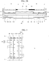
- FIG. 1 is a view schematically showing a lay-out of an organic light-emitting display device according to an embodiment of the present invention.
- FIG. 2A is a cross-section view schematically the organic light-emitting display device according to the embodiment of the present invention.
- FIG. 2B is a view taken along I-I' of FIG. 1
- the organic light-emitting display device may comprise a lower substrate 100, an auxiliary electrode 410, light-emitting structure 500 and a connecting clad electrode 650.
- the lower substrate 100 may support the light-emitting structure 500.
- the lower substrate 100 may include an insulating material.
- the lower substrate 100 may include glass or plastic.
- the lower substrate 100 may include pixel areas. Each of the pixel areas may include an emission area EA and a transparent area TA.
- the emission area EA may display a color for realizing an image.
- a plurality of the light-emitting structures 500 may be disposed in the light-emitting area EA.
- a blue light-emitting structure for displaying a blue color a red light-emitting structure for displaying a red color
- the transparent area TA may be transparent.
- a gate line GL, data lines DL1-DL4, a sensing line SL, a reference voltage supply line Vref and a power supply line VDD may be disposed on the lower substrate 100.
- the gate line GL may extend in a direction.
- the data lines DL1-DL4 may intersect the gate line GL.
- the data lines DL1-DL4 may transmit a data signal to the light-emitting structure 500 disposed in the emission area EA.
- the organic light-emitting display device may include four data lines DL1-DL4.
- the sensing line SL may be parallel with the gate line SL.
- the reference voltage supply line Vref and the power supply line VDD may be parallel with the data lines DL1-DL4.
- the gate line GL, the data lines DL1-DL4, the sensing line SL, the reference voltage supply line Vref and the power supply line VDD may define a sub emission area in the emission area EA.
- a circuit for controlling one of the light-emitting structures 500 may be disposed in each of the sub emission area.
- each of the emission areas EA may include four sub emission areas separated by the gate line GL, the data lines DL1-DL4, the sensing line SL, the reference voltage supply line Vref and the power supply line VDD.
- a selective thin film transistor TR1, a driving thin film transistor TR2, a sensing thin film transistor TR3 and a storage capacitor Cst may be disposed in each sub emission area.
- the selective thin film transistor TR1 may turn on/off the driving thin film transistor according to a gate signal applied by the gate line GL.
- the driving thin film transistor TR2 may supply a driving current to corresponding light-emitting structure 500 according to a signal of the selective thin film transistor TR1 and a data signal applied by corresponding data line DL1-DL4.
- the degree of deterioration of each driving thin film transistor TR2 and/or each light-emitting structure 500 may be detected by corresponding sensing thin film transistor TR3.
- the storage capacitor Cst may maintain the signal of the selective thin film transistor TR1 applied to the driving thin film transistor TR2 for a certain period of time.
- the driving thin film transistor TR2 may includes a semiconductor pattern 210, a gate insulating layer 220, a gate electrode 230, an interlayer insulating layer 240, a source electrode 250 and a drain electrode 260, as shown in FIG. 2A .
- the semiconductor pattern 210 may be disposed on the lower substrate 100.
- the semiconductor pattern 210 may include a semiconductor material.
- the semiconductor pattern 210 may include amorphous silicon or polycrystalline silicon.
- the semiconductor pattern 210 may include an oxide semiconductor material.
- the semiconductor pattern 210 may include IGZO.
- the semiconductor pattern 210 may include a source region, a drain region and a channel region.
- the channel region may be disposed between the source region and the drain region.
- Conductivity of the channel region may be lower than conductivities of the source region and the drain region.
- the source region and the drain region may include a conductive impurity.
- the organic light-emitting display device is described that the semiconductor pattern 210 of each thin film transistor TR1, TR2 and TR3 is in direct contact with the lower substrate 100.
- the organic light-emitting display device may further include a buffer layer disposed between the lower substrate 100 and the thin film transistors TR1, TR2 and TR3.
- the buffer layer may be extended beyond the semiconductor pattern 210.
- the buffer layer may cover the entire surface of the lower substrate 100.
- the buffer layer may include an insulating material.
- the buffer layer may include silicon oxide.
- the gate insulating layer 220 may be disposed on the semiconductor pattern 210.
- the gate insulating layer 220 may include an insulating material.
- the gate insulating layer 220 may include silicon oxide and/or silicon nitride.
- the gate insulating layer 220 may have a multi-layer structure.
- the gate insulating layer 220 may include a high-K material.
- the gate insulating layer 220 may include hafnium oxide (HfO) or titanium oxide (TiO).
- the gate electrode 230 may be disposed on the gate insulating layer 220.
- the gate electrode 230 may overlap the channel region of the semiconductor pattern 210.
- the gate electrode 230 may be insulated from the semiconductor pattern 210 by the gate insulating layer 220.
- the gate insulating layer 220 may include a side surface vertically align with a side surface of the gate electrode 230.
- the side surface of the gate insulating layer 220 may be continuously with the side surface of the gate electrode 230.
- the gate electrode 230 may include a conductive material.
- the gate electrode 230 may include a metal, such as aluminum (Al), chrome (Cr), cupper (Cu), titanium (Ti), molybdenum (Mo) and tungsten (W).
- the gate electrode 230 may have a multi-layer structure.
- the gate line GL which is shown in FIG. 1 may include a material same as the gate electrode 230.
- the gate electrode 230 may be disposed on a layer same as the gate line GL.
- a structure of the gate line GL may be the same as a structure of the gate electrode 230.
- the interlayer insulating layer 240 may be disposed on the semiconductor pattern 210 and the gate electrode 230.
- the interlayer insulating layer 240 may be extended beyond the semiconductor pattern 210.
- the interlayer insulating layer 240 may be in direct contact with the buffer layer in the outside of the semiconductor pattern 210.
- the interlayer insulating layer 240 may include an insulating material.
- the interlayer insulating layer 240 may include silicon oxide.
- the source electrode 250 and the drain electrode 260 may be disposed on the interlayer insulating layer 240.
- the source electrode 250 may be electrically connected to the source region of the semiconductor pattern 210.
- the drain electrode 260 may be electrically connected to the drain region of the semiconductor pattern 210.
- the interlayer insulating layer 240 may include a first interlayer contact hole 241h exposing the source region of the semiconductor pattern 210 and a second interlayer contact hole 242h exposing the drain region of the semiconductor pattern 210.
- the drain electrode 260 may be spaced apart from the source electrode 250.
- the source electrode 250 and the drain electrode 260 may include a conductive material.
- the source electrode 250 and the drain electrode 260 may include metal, such as aluminum (Al), chrome (Cr), cupper (Cu), titanium (Ti), molybdenum (Mo) and tungsten (W).
- the drain electrode 260 may include a material same as the source electrode 250.
- the source electrode 250 may have a multi-layer structure.
- a structure of the drain electrode 260 may be the same as a structure of the source electrode 250.
- the drain electrode 260 may have a multi-layer structure.
- the data lines DL1-DL4, the reference voltage supply line Vref and the power supply line VDD which are shown in FIG. 1 may include a material same as the source electrode 250 and the drain electrode 260.
- the data lines DL1-DL4, the reference voltage supply line Vref and the power supply line VDD may be disposed on a layer same as the source electrode 250 and the drain electrode 260.
- the data lines DL1-DL4, the reference voltage supply line Vref and the power supply line VDD may be disposed on the interlayer insulating layer 240.
- Structures of the data lines DL1-DL4, the reference voltage supply line Vref and the power supply line VDD may be the same as the structure of the source electrode 250 and the structure of the drain electrode 260.
- the data lines DL1-DL4 and the power supply line VDD may have a multi-layer structure.
- each of the thin film transistors TR1, TR2 and TR3 includes the interlayer insulating layer 240 between gate electrode 230 and source/drain electrode 250 and 260.
- each of the thin film transistors TR1, TR2 and TR3 may include a gate insulating layer 220 between the gate electrode 230 and the source/drain electrodes 250 and 260.
- the storage capacitor Cst may be spaced apart from the thin film transistors TR1, TR2 and TR3, as shown in FIG. 2A .
- the storage capacitor Cst may be electrically connected to the thin film transistors TR1, TR2 and TR3.
- the storage capacitor Cst may include a lower capacitor electrode 310, a capacitor insulating layer 320 and an upper capacitor electrode 330, which are sequentially stacked.
- the lower capacitor electrode 310 and the upper capacitor electrode 330 may include a conductive material.
- the lower capacitor electrode 310 may include a material same as the gate electrode 230.
- a structure of the lower capacitor electrode 310 may be the same as the structure of the gate electrode 230.
- the upper capacitor electrode 330 may include a material same as the source electrode 250 and the drain electrode 260.
- a structure of the upper capacitor electrode 330 may be the same as the structure of the source electrode 250 and the structure of the drain electrode 260.
- the upper capacitor electrode 330 may be connected to the drain electrode 260 of the driving thin film transistor TR2.
- the upper capacitor electrode 330 may have a multi-layer structure.
- the capacitor insulating layer 320 may include an insulating material.
- the capacitor insulating layer 320 may include silicon oxide.
- the capacitor insulating layer 320 may include a material same as the interlayer insulating layer 240.
- the capacitor insulating layer 320 may be continuously with the interlayer insulating layer 240.
- the organic light-emitting display device may further include a lower insulating layer 301 between the lower substrate 100 and the storage capacitor Cst.
- a side surface of the lower insulating layer 301 may be continuously with a side surface of the lower capacitor electrode 310.
- the lower insulating layer 301 may include a material same as the gate insulating layer 220.
- a dummy pattern WL may be disposed on the lower substrate 100.
- the dummy pattern WL may extend along a direction parallel with the data lines DL1-DL4.
- the dummy pattern WL may extend between the emission area EA and the transparent area TA.
- the dummy pattern WL may include a region overlapping with the transparent area TA of the lower substrate 100.
- the dummy pattern WL may include a conductive material.
- the dummy pattern WL may include a material same as one of conductive layers of the thin film transistors TR1, TR2 and TR3.
- the dummy pattern WL may include a material same as the source electrode 250 and the drain electrode 260.
- the dummy pattern WL may include a material same as the data lines DL1-DL4.
- the organic light-emitting display device may further include a lower passivation layer 130 on the thin film transistors TR1, TR2 and TR3, the storage capacitor Cst and the dummy pattern WL.
- the lower passivation layer 130 may prevent the thin film transistors TR1, TR2 and TR3 from the external moisture and the hydrogen.
- the thin film transistors TR1, TR2 and TR3, the storage capacitor Cst and the dummy pattern WL may be covered by the lower passivation layer 130.
- the lower passivation layer 130 may include an insulating material.
- the lower passivation layer 130 may include silicon oxide and/or silicon nitride.
- the auxiliary electrode 410 may be disposed on the lower passivation layer 130.
- the auxiliary electrode 410 may be disposed in the emission area EA.
- the auxiliary electrode 410 may be disposed on the thin film transistors TR1, TR2 and TR3.
- the auxiliary electrode 410 may include a conductive material.
- the auxiliary electrode 410 may include a metal, such as copper (Cu), molybdenum (Mo), titanium (Ti), aluminum (Al) and tungsten (W).
- the auxiliary electrode 410 may have a multi-layer structure.
- the auxiliary electrode 410 may include a lower auxiliary electrode 411 and an upper auxiliary electrode 412 disposed on the lower auxiliary electrode 411.
- the organic light-emitting display device may further include an auxiliary clad electrode 450 on the auxiliary electrode 410.
- the auxiliary clad electrode 450 may prevent the auxiliary electrode 410 from being damaged by the subsequent process.
- the auxiliary electrode 410 may be covered by the auxiliary clad electrode 450.
- the auxiliary clad electrode 450 may include a conductive material.
- the auxiliary clad electrode 450 may include a material having low reactivity.
- the auxiliary clad electrode 450 may include a material having high transmissivity.
- the auxiliary clad electrode 450 may include a conductive oxide, such as ITO or IZO.
- the organic light-emitting display device may further include a lower over-coat layer 140 between the lower passivation layer 130 and the auxiliary electrode 410.
- the lower over-coat layer 140 may remove the thickness difference due to the thin film transistors TR1, TR2 and TR3 and the storage capacitor Cst.
- an upper surface of the lower over-coat layer 140 opposite to the lower substrate 100 may be flat surface.
- the upper surface of the lower over-coat layer 140 may be parallel with a surface of the lower substrate 100.
- the lower over-coat layer 140 may include an insulating material.
- the lower over-coat layer 140 may include an organic insulating material.
- the light-emitting structure 500 may generate the light realizing a specific color.
- the light-emitting structure 500 may be disposed in the emission area EA.
- the light-emitting structure 500 may be disposed on the auxiliary electrode 410.
- the light-emitting structure 500 may include a lower emission electrode 510, an organic light-emitting layer 520, and an upper emission electrode 530, which are sequentially stacked.
- the organic light-emitting display device may further include an upper over-coat layer 150 between the auxiliary electrode 410 and the light-emitting structure 500.
- the upper over-coat layer 150 may remove the thickness difference due to the auxiliary electrode 410.
- an upper surface of the upper over-coat layer 150 facing the light-emitting structure 500 may be a flat surface.
- the upper surface of the upper over-coat layer 150 may be parallel with the upper surface of the lower over-coat layer 140.
- the upper over-coat layer 150 may included an insulating material.
- the upper over-coat layer 150 may include an organic insulating material.
- the upper over-coat layer 150 may include a material different from the lower over-coat layer 140.
- the lower emission electrode 510 may include a conductive material.
- the lower emission electrode 510 may include a material having high reflective.
- the lower emission electrode 510 may include a reflective layer having a metal, such as aluminum (Al) and silver (Ag).
- the lower emission electrode 510 may have a multi-layer structure.
- the lower emission electrode 510 may have a structure in which a reflective layer including a material with high reflective is disposed between transparent electrodes including conductive oxide, such as ITO.
- the organic light-emitting layer 520 may generate light having luminance corresponding to a voltage difference between the lower emission electrode 510 and the upper emission electrode 530.
- the organic light-emitting layer 520 may include an emission material layer (EML) having an organic emission material.
- EML emission material layer
- the organic light-emitting layer 520 may have a multi-layer structure in order to increase luminous efficacy.
- the organic light-emitting layer 520 may further include at least one of a hole injection layer (HIL), a hole transport layer (HTL), an electron transport layer (ETL), and an electron injection layer (EIL).
- HIL hole injection layer
- HTL hole transport layer
- ETL electron transport layer
- EIL electron injection layer
- the upper emission electrode 530 may include a conductive material.
- the upper emission electrode 530 may include a material different from the lower emission electrode 510.
- the upper emission electrode 530 may be a transparent electrode.
- the light generated by the organic light-emitting layer 520 may be emitted through the upper emission electrode 530.
- the connecting clad electrode 650 may connect the lower emission electrode 510 of the light-emitting structure 500 to corresponding driving thin film transistor TR2.
- the light-emitting structure 500 may be controlled by corresponding thin film transistors TR1, TR2 and TR3.
- the connecting clad electrode 650 may be disposed between the lower over-coat layer 140 and the upper over-coat layer 150.
- the lower passivation layer 130 may include an electrode contact hole 131h exposing a portion of the upper capacitor electrode 330 which is connected to the drain electrode 260 of corresponding driving thin film transistor TR2.
- the lower over-coat layer 140 may include a lower contact hole 141h overlapping with the electrode contact hole 131h.
- the upper over-coat layer 150 may include an upper contact hole 151h exposing a portion of the connecting clad electrode 650.
- the upper contact hole 151h may be spaced apart from the lower contact hole 141h.
- the connecting clad electrode 650 may include a first clad region 651 including a portion overlapping with the lower contact hole 151h, a second clad region 652 including a portion overlapping with the upper contact hole 151h and a repair cutting region 653 between the first clad region 651 and the second clad region 652, as shown in FIG. 2B .
- the repair cutting region 653 may overlap with the transparent area TA of the lower substrate 100.
- the repair cutting region 653 may be disposed in a laser cutting area where the laser is irradiated in the repair process.
- the connecting clad electrode 650 may include a conductive material. Transmissivity of the connecting clad electrode 650 may be higher than transmissivity of the lower emitting electrode 510.
- the connecting clad electrode 650 may include a conductive oxide.
- the connecting clad electrode 650 may include a material same as the auxiliary clad electrode 450.
- the connecting clad electrode 650 may include ITO or IZO.
- the connecting clad electrode 650 connecting the lower emission electrode 510 to corresponding driving thin film transistor TR2 may include the repair cutting region 653.
- the luminous efficacy of the light-emitting structure 500 may not be influenced by the transmissivity of the repair cutting region 653. That is, in the organic light-emitting display device according to the embodiment of the present invention, since the connecting clad electrode 650 including the repair cutting region 653 has higher transmissivity than the lower emission electrode 510, the reduction of the area of the transparent area TA due to the repair cutting region 653 may be prevented without losing the luminous efficacy.
- the organic light-emitting display device may further include a first connection electrode 610 electrically connecting the connecting clad electrode 650 to the drain electrode 260 of corresponding driving thin film transistor TR2.
- the first connection electrode 610 may be disposed between the lower over-coat layer 140 and the upper over-coat layer 150.
- the connecting clad electrode 650 may extend onto the first connection electrode 610.
- the first connection electrode 610 may be covered by the first clad region 651 of the connecting clad electrode 650.
- the first connection electrode 610 may be extended along the electrode contact hole 131h and the lower contact hole 141h.
- the first connection electrode 610 may be connected to the upper capacitor electrode 330 through the electrode contact hole 131h and the lower contact hole 141h.
- the first connection electrode 610 may include a conductive material. Conductivity of the first connection electrode 610 may be higher than conductivity of the connecting clad electrode 650.
- the first connection electrode 610 may include a metal, such as copper (Cu), molybdenum (Mo), titanium (Ti), aluminum (Al) and tungsten (W). Transmissivity of the first connection electrode 610 may be lower than transmissivity of the connecting clad electrode 650.
- a structure of the first connection electrode 610 may be the same as the structure of the auxiliary electrode 410.
- the first connection electrode 610 may have a multi-layer structure.
- the first connection electrode 610 may include a first lower connection electrode 611 and a first upper connection electrode 612 disposed on the first lower connection electrode 611.
- the first lower connection electrode 611 may include a material same as the lower auxiliary electrode 411.
- the first upper connection electrode 612 may include a material same as the upper auxiliary electrode 412.
- the first connection electrode 610 may be disposed on the emission area EA of the lower substrate 100.
- the first connection electrode 610 may be extended along the connecting clad electrode 650 on the emission area EA of the lower substrate 100.
- the resistance between the light-emitting structure 500 and corresponding driving thin film transistor TR2 which are electrically connected by the connecting clad electrode 650 may be reduced.
- the organic light-emitting display device may further include a second connection electrode 620 between the lower over-coat layer 140 and the second clad region 652 of the connecting clad electrode 650.
- the second connection electrode 620 may include a portion overlapping with the upper contact hole 151h of the upper over-coat layer 150.
- the second clad region 652 of the connecting clad electrode 650 may cover the second connection electrode 620.
- the second connection electrode 620 may include a conductive material. Conductivity of the second connection electrode 652 may be higher than the conductivity of the connecting clad electrode 650.
- the second connection electrode 620 may include a metal, such as copper (Cu), molybdenum (Mo), titanium (Ti), aluminum (Al) and tungsten (W).
- the conductivity of the second connection electrode 620 may be the same as the conductivity of the first connection electrode 610.
- Transmissivity of the second connection electrode 620 may be lower than the transmissivity of the connecting clad electrode 650.
- the transmissivity of the second connection electrode 620 may be the same as the transmissivity of the first connection electrode 610.
- a structure of the second connection electrode 620 may be the same as the structure of the first connection electrode 610.
- the second connection electrode 620 may have a multi-layer structure.
- the structure of the second connection electrode 620 may be the same as the structure of the auxiliary electrode 410.
- the second connection electrode 620 may include a second lower connection electrode 621 and a second upper connection electrode 622 disposed on the second lower connection electrode 621.
- the second lower connection electrode 621 may include a material same as the first lower connection electrode 611.
- the second upper connection electrode 622 may include a material same as the first upper connection electrode 612.
- the second connection electrode 620 may be disposed in the emission area EA of the lower substrate 100.
- the second connection electrode 620 may be extended along the connecting clad electrode 650 on the emission area EA of the lower substrate 100.
- the organic light-emitting display device may further include a bank insulating layer 160 in order to insulate adjacent light-emitting structures 500.
- the bank insulating layer 160 may cover an edge of the lower emission electrode 510 of each light-emitting structure 500.
- the organic light-emitting layer 520 and the upper emission electrode 530 may be stacked on a portion of the lower emitting electrode 510 exposed by the bank insulating layer 160.
- the bank insulating layer 160 may include an insulating material.
- the bank insulating layer 160 may include an organic insulating material, such as benzocyclobutene (BCB), poly-imide or photo-acryl.
- the lower over-coat layer 140 and the upper over-coat layer 150 may include a material different from the bank insulating layer 160.
- the organic light-emitting layer 520 and the upper emission electrode 530 may be extended onto the bank insulating layer 160.
- the upper emission electrode 530 may be connected to the auxiliary electrode 410, as shown in FIG. 2A .
- the luminance unevenness due to the voltage drop of the upper emission electrode 530 may be prevented.
- the organic light-emitting display device may further include a partition 700 in order to provide a space for electrically connecting the upper emission electrode 530 to the auxiliary electrode 410.
- a portion of the organic light-emitting layer 520 may separated from another portion of the organic light-emitting layer 520 by the partition 700.
- the upper emission electrode 530 may be electrically connected to the auxiliary electrode 410 through the space between the separated portions of the organic light-emitting layer 520 separated by the partition 700.
- a vertical distance of the partition 700 may be larger than a vertical thickness of the bank insulating layer 160.
- the partition 700 may include a lower partition 710 and an upper partition 720 disposed on the lower partition 710.
- the lower partition 710 and the upper partition 720 may include an insulating material.
- the lower partition 710 may include a material same as the bank insulating layer 160.
- the upper partition 720 may include a material different from the lower partition 710.
- the upper partition 720 may include silicon oxide and/or silicon nitride.
- the organic light-emitting display device may further include an intermediate electrode 550 between the auxiliary electrode 410 and the bank insulating layer 160.
- the intermediate electrode 550 may be connected to the auxiliary electrode 410.
- the upper over-coat layer 150 may include a penetrating hole 152h exposing a portion of the auxiliary electrode 410.
- the partition 700 may overlap with the intermediate electrode 550.
- the organic light-emitting layer 520 may expose a portion of the intermediate electrode 550 by the partition 700.
- the bank insulating layer 160 may cover an edge of the intermediate electrode 550.
- the partition 700 may be disposed in an opening of the bank insulating layer 160.
- the upper emitting electrode 530 may be contact with the portion of the intermediate electrode 550 which is not covered by the organic light-emitting layer 520 due to the partition 700.
- the upper emission electrode 530 may be electrically connected to the auxiliary electrode 410 through the intermediate electrode 550.
- the intermediate electrode 550 may include a conductive material.
- the intermediate electrode 550 may include a material same as the lower emission electrode 510.
- the intermediate electrode 550 may have a multi-layer structure.
- a structure of the intermediate electrode 550 may be the same as the structure of the lower emission electrode 510.
- the organic light-emitting display device may further include an upper substrate 800 opposite the lower substrate 100.
- the upper substrate 800 may overlap with the emission area EA and the transparent area TA of the lower substrate 100.
- the upper substrate 800 may be disposed on the light-emitting structure 500.
- the upper substrate 800 may include an insulating material.
- the upper substrate 800 may include a transparent material.
- the upper substrate 800 may include glass or plastic.
- the light-emitting structure 500 of each sub emission area may display the same color.
- the light-emitting structure 500 of each sub emission area may include a white organic light-emitting layer 520.
- the organic light-emitting display device according to the embodiment of the present invention may further include a black matrix 810 and a color filter 820 on the upper substrate 800.
- the sub emission areas in which the light-emitting structure 500 realizing the same color are disposed may display different colors.
- the organic light-emitting display device may further include a filler 900 filling a space between the lower substrate 100 and the upper substrate 800.
- the filler 900 may prevent the light-emitting structure 500 from being damaged by the external impact.
- the filler 900 may extend between the light-emitting structure 500 and the color filter 820, and between the upper emitting electrode 530 and the black matrix 810.
- the organic light-emitting display device is described that the light-emitting structure 500 is in direct contact with the filler 900.
- the organic light-emitting display device may further include an upper passivation layer between the light-emitting structure 500 and the filter 900.
- the upper passivation layer may prevent the external moisture from permeating into the light-emitting structure 500.
- the upper passivation layer may have a multi-layer structure.
- the upper passivation layer may have a structure in which an inorganic layer including an inorganic material and a organic layer including an organic material are stacked.
- the connecting clad electrode 650 which does not affect the luminous efficiency of the structure may include a repair cutting region 653 overlapping with the transparent area TA of the lower substrate 100, and the connecting clad electrode 650 may have higher transmissivity than the lower emitting electrode 510, so that, regardless of the area of the emission area EA and the luminous efficiency of the light-emitting structure 500, the reduction in the area of the transmissivity area TA due to the repair cutting region 653 may be prevented.
- the transparency of the transparent area TA may be improved without losing the aperture ratio and the luminescent efficiency of the emission area EA.
- the organic light-emitting display device is described that the first connection electrode 610 and the second connection electrode 620 are extended along the connecting clad electrode 650 on the emission area EA.
- the first clad region 651 and the second clad region 652 extending onto the emission area EA from the repair cutting region 653 of the connecting clad electrode 650 overlapping with the transparent area TA may not overlap with the first connection electrode 610 or the second connection electrode 620, as shown in FIG. 3 .
- the reduction of the area of the transparent area TA by the repair cutting region 653 may be effectively prevented.
- the organic light-emitting display device is described that the connecting clad electrode 650 of each sub emission area is connected to corresponding storage capacitor Cst under the lower emission electrode 510 of adjacent sub emission area.
- the connecting clad electrodes 650 may be arranged in various ways.
- points at which the connecting clad electrodes 650 including the repair cutting region 653 located in the same direction are connected to the storage capacitor Cst may be disposed adjacent to each other, as shown in FIG. 4 .
- the degree of freedom for arrangement of signal lines and/or voltage supply lines may be improved.
- the organic light-emitting display device is described that the circuits of four sub emission area disposed in the single emission area is arranged parallel with the data lines DL1-DL4.
- the circuits of sub emission areas may be arranged in various ways.
- the circuits of each sub emission area may be arranged in a quad type.
- the aperture ratio of the emission area and the area of the transparent area may be maximized.
- the organic light-emitting display device may include a repair cutting region consist of a conductive layer having higher transmissivity than a lower emission electrode.
- a repair cutting region consist of a conductive layer having higher transmissivity than a lower emission electrode.
Landscapes
- Engineering & Computer Science (AREA)
- Microelectronics & Electronic Packaging (AREA)
- Physics & Mathematics (AREA)
- Geometry (AREA)
- Optics & Photonics (AREA)
- Manufacturing & Machinery (AREA)
- Electroluminescent Light Sources (AREA)
- Devices For Indicating Variable Information By Combining Individual Elements (AREA)
Abstract
Description
- This application claims the priority benefit of Korean Patent Application No.
10-2016-0184361, filed on December 30, 2016 - The present invention relates to an organic light-emitting display device in which a thin film transistor and a light-emitting structure are connected by a connecting clad electrode.
- Generally, an electronic appliance, such as a monitor, a TV, a laptop computer, and a digital camera, include a display device to realize an image. For example, the display device may include a liquid crystal display device and an organic light-emitting display device.
- The organic light-emitting display device may be a transparent display device. For example, each pixel area of the organic light-emitting display device may include an emission area and a transparent area. A light-emitting structure and a circuit for controlling the light-emitting structure may be disposed in the emission area. The external light may transmit the transparent area.
- The emission area may display various color for realizing an image. For example, a blue light-emitting structure for displaying a blue color, a red light-emitting structure for displaying a red color, a green light-emitting structure for displaying a green color and a white light-emitting structure for display a white color are disposed in the emission area. Each of the light-emitting structure may include a lower emission electrode, an organic light-emitting layer and an upper emission electrode, which area sequentially stacked.
- A defect of some light-emitting structures may occur due to a particle generated in a process of forming the organic light-emitting display device. The process of forming the organic light-emitting display device may include a repair process in order to minimize decrease of an image quality caused by defective light-emitting structures. For example, the repair process of the organic light-emitting display device may include a step of electrically disconnecting the lower emission electrode which is shortcircuited with the upper emission electrode by the particles from corresponding circuit.
- The step of electrically disconnecting the lower emission electrode of the light-emitting structure which has a defect from the corresponding circuit may include a laser cutting process. For example, the repair process of the organic light-emitting display device may include a step of cutting a portion of the lower emission electrode using the laser. For the convenience of the process, the repair cutting region of the lower emission electrode cut by the repair process may overlap with the transparent area of the lower substrate.
- However, since the lower emission electrode of the organic light-emitting display device includes a reflective layer, the area of the transparent area may be reduced due to the repair cutting region. Also, in the organic light-emitting display device, the repair cutting region may be disposed in the light-emitting area of the lower substrate to prevent reducing the area of the transparent, but the opening of the emission area may be reduced. Thus, in the organic light-emitting display device, the luminous efficacy may be decreased and the element adjacent to the repair cutting area may be damaged by the repair process.
- Accordingly, embodiments of the present disclosure are directed to an organic light-emitting display device having a connecting clad electrode that substantially obviates one or more of the problems due to limitations and disadvantages of the related art
- An aspect of the present disclosure is to provide an organic light-emitting display device capable of preventing decreasing of the area of the transparent by a repair cutting region.
- Another aspect of the present disclosure is to provide an organic light-emitting display device which may increase a transmissivity of a transparent area without reducing an opening of a light-emitting area.
- Additional features and aspects will be set forth in the description that follows, and in part will be apparent from the description, or may be learned by practice of the inventive concepts provided herein. Other features and aspects of the inventive concepts may be realized and attained by the structure particularly pointed out in the written description, or derivable therefrom, and the claims hereof as well as the appended drawings.
- To achieve these and other aspects of the inventive concepts, as embodied and broadly described, an organic light-emitting display device according to claim 1 is provided. Further embodiments are described in the dependent claims. In an aspect, an organic light-emitting display device comprises a lower substrate. The lower substrate includes an emission area and a transparent area. A thin film transistor is disposed on the emission area of the lower substrate. A light-emitting structure is disposed on the thin film transistor. The light-emitting structure includes a lower emission electrode, an organic light-emitting layer and an upper emission electrode, which are sequentially stacked. The light-emitting structure is electrically connected to the thin film transistor by a connecting clad electrode. The connecting clad electrode has the transmissivity higher than the lower emission electrode. The connecting clad electrode includes a repair cutting region overlapping with the transparent area of the lower substrate.
- The connecting clad electrode may include a conductive oxide such as ITO.
- The lower emission electrode may include a reflective layer.
- A lower over-coat layer may be disposed between the thin film transistor and the connecting clad electrode, the lower over-coat layer including a lower penetrating hole. An upper over-coat layer may be disposed between the connecting clad electrode and the light-emitting structure, the upper over-coat layer including an upper penetrating hole spaced apart from the lower penetrating hole.
- A first connection electrode may be disposed between the thin film transistor and the connecting clad electrode. The first connection electrode may be connected to the thin film transistor. The connecting clad electrode may further include a first clad region covering the first connection electrode.
- The first connection electrode may be disposed between the lower over-coat layer and the upper over-coat layer, the first connection electrode connected to the thin film transistor through the lower penetrating hole.
- The first connection electrode may be extended along the connecting clad electrode on the emission area of the lower substrate.
- A second connection electrode may be disposed between the lower over-coat layer and the connecting clad electrode. The second connection electrode may be spaced apart from the first connection electrode. The second connection electrode may include a region overlapping with the upper penetrating hole. The connecting clad electrode may further include a second clad region covering the second connection electrode. The repair cutting region may be disposed between the first clad region and the second clad region.
- A structure of the second connection electrode may be the same as a structure of the first connection electrode.
- The second connection electrode may be extended along the connecting clad electrode on the emission area of the lower substrate.
- The connecting clad electrode may have a transmissivity higher than the first connection electrode, the second connection electrode and the lower emission electrode.
- An auxiliary electrode may be disposed between the lower over-coat layer and the upper over-coat layer; and an auxiliary clad electrode may cover the auxiliary electrode, the auxiliary clad electrode spaced apart from the first connection electrode, the second connection electrode and the connecting clad electrode, wherein the connecting clad electrode includes a material same as the auxiliary clad electrode.
- A structure of the first connection electrode and a structure of the second connection electrode may be the same as a structure of the auxiliary electrode.
- In another aspect, an organic light-emitting display device comprises a lower substrate. The lower substrate includes an emission area and a transparent area. A thin film transistor is disposed on the emission area of the lower substrate. A lower over-coat layer is disposed on the thin film transistor. The lower over-coat layer includes a lower penetrating hole exposing a portion of the thin film transistor. A first connection electrode is disposed on the lower over-coat layer. The first connection electrode is connected to the thin film transistor through the lower penetrating hole. A second connection electrode is disposed on the lower over-coat layer. The second connection electrode is spaced apart from the first connection electrode. An upper over-coat layer is disposed on the first connection electrode and the second connection electrode. The upper over-coat layer may cover the first connection electrode and the second connection electrode. The upper over-coat layer includes an upper penetrating hole overlapping with the second connection electrode. A light-emitting structure is disposed on the upper over-coat layer. The light-emitting structure includes a lower emission electrode connected to the second connection electrode through the upper penetrating hole. A connecting clad electrode is disposed between the lower over-coat layer and the upper over-coat layer. The connecting clad electrode is connected between the first connection electrode and the second connection electrode. The connecting clad electrode includes a repair cutting region overlapping with the transparent area of the lower substrate.
- The connecting clad electrode may have a transmissivity higher than the first connection electrode, the second connection electrode and the lower emission electrode.
- An auxiliary electrode may be disposed between the lower over-coat layer and the upper over-coat layer. An auxiliary clad electrode may cover the auxiliary electrode, the auxiliary clad electrode spaced apart from the first connection electrode, the second connection electrode and the connecting clad electrode. The connecting clad electrode may include a material same as the auxiliary clad electrode.
- A structure of the first connection electrode and a structure of the second connection electrode may be the same as a structure of the auxiliary electrode.
- It is to be understood that both the foregoing general description and the following detailed description are exemplary and explanatory and are intended to provide further explanation of the inventive concepts as claimed.
- The accompanying drawings, which are included to provide a further understanding of the disclosure and are incorporated and constitute a part of this application, illustrate embodiments of the disclosure and together with the description serve to explain various principles. In the drawings:
-
FIG. 1 is a view schematically showing a lay-out of an organic light-emitting display device according to an embodiment of the present invention; -
FIG. 2A is a cross-section view schematically showing the organic light-emitting display device according to the embodiment of the present invention; -
FIG. 2B is a view taken along I-I' ofFIG. 1 -
FIGs. 3 to 5 are respectively various examples of an organic light-emitting display device according to another embodiment of the present invention. - Hereinafter, details related to the above objects, technical configurations, and operational effects of the embodiments of the present invention will be clearly understood by the following detailed description with reference to the drawings, which illustrate some embodiments of the present invention. Here, the embodiments of the present invention are provided in order to allow the technical sprit of the present invention to be satisfactorily transferred to those skilled in the art, and thus the present invention may be embodied in other forms and is not limited to the embodiments described below.
- In addition, the same or extremely similar elements may be designated by the same reference numerals throughout the specification, and in the drawings, the lengths and thickness of layers and regions may be exaggerated for convenience. It will be understood that, when a first element is referred to as being "on" a second element, although the first element may be disposed on the second element so as to come into contact with the second element, a third element may be interposed between the first element and the second element.
- Here, terms such as, for example, "first" and "second" may be used to distinguish any one element with another element. However, the first element and the second element may be arbitrary named according to the convenience of those skilled in the art without departing the technical sprit of the present invention.
- The terms used in the specification of the present invention are merely used in order to describe particular embodiments, and are not intended to limit the scope of the present invention. For example, an element described in the singular form is intended to include a plurality of elements unless the context clearly indicates otherwise. In addition, in the specification of the present invention, it will be further understood that the terms "comprises" and "includes" specify the presence of stated features, integers, steps, operations, elements, components, and/or combinations thereof, but do not preclude the presence or addition of one or more other features, integers, steps, operations, elements, components, and/or combinations.
- Unless otherwise defined, all terms (including technical and scientific terms) used herein have the same meaning as commonly understood by one of ordinary skill in the art to which example embodiments belong. It will be further understood that terms, such as those defined in commonly used dictionaries, should be interpreted as having a meaning that is consistent with their meaning in the context of the relevant art and should not be interpreted in an idealized or overly formal sense unless expressly so defined herein.
-
FIG. 1 is a view schematically showing a lay-out of an organic light-emitting display device according to an embodiment of the present invention.FIG. 2A is a cross-section view schematically the organic light-emitting display device according to the embodiment of the present invention.FIG. 2B is a view taken along I-I' ofFIG. 1 - Referring to
FIGs. 1, 2A and2B , the organic light-emitting display device according to the embodiment of the present invention may comprise alower substrate 100, anauxiliary electrode 410, light-emittingstructure 500 and a connectingclad electrode 650. - The
lower substrate 100 may support the light-emittingstructure 500. Thelower substrate 100 may include an insulating material. For example, thelower substrate 100 may include glass or plastic. - The
lower substrate 100 may include pixel areas. Each of the pixel areas may include an emission area EA and a transparent area TA. The emission area EA may display a color for realizing an image. A plurality of the light-emittingstructures 500 may be disposed in the light-emitting area EA. For example, a blue light-emitting structure for displaying a blue color, a red light-emitting structure for displaying a red color, a green light-emitting structure for displaying a green color and a white light-emitting structure for display a white color may be disposed in the emission area EA. The transparent area TA may be transparent. - As shown in
FIG. 1 , a gate line GL, data lines DL1-DL4, a sensing line SL, a reference voltage supply line Vref and a power supply line VDD may be disposed on thelower substrate 100. The gate line GL may extend in a direction. The data lines DL1-DL4 may intersect the gate line GL. The data lines DL1-DL4 may transmit a data signal to the light-emittingstructure 500 disposed in the emission area EA. For example, the organic light-emitting display device according to the embodiment of the present invention may include four data lines DL1-DL4. The sensing line SL may be parallel with the gate line SL. The reference voltage supply line Vref and the power supply line VDD may be parallel with the data lines DL1-DL4. - The gate line GL, the data lines DL1-DL4, the sensing line SL, the reference voltage supply line Vref and the power supply line VDD may define a sub emission area in the emission area EA. For example, a circuit for controlling one of the light-emitting
structures 500 may be disposed in each of the sub emission area. In the organic light-emitting display device according to the embodiment of the present invention, each of the emission areas EA may include four sub emission areas separated by the gate line GL, the data lines DL1-DL4, the sensing line SL, the reference voltage supply line Vref and the power supply line VDD. For example, a selective thin film transistor TR1, a driving thin film transistor TR2, a sensing thin film transistor TR3 and a storage capacitor Cst may be disposed in each sub emission area. - The selective thin film transistor TR1 may turn on/off the driving thin film transistor according to a gate signal applied by the gate line GL. The driving thin film transistor TR2 may supply a driving current to corresponding light-emitting
structure 500 according to a signal of the selective thin film transistor TR1 and a data signal applied by corresponding data line DL1-DL4. The degree of deterioration of each driving thin film transistor TR2 and/or each light-emittingstructure 500 may be detected by corresponding sensing thin film transistor TR3. The storage capacitor Cst may maintain the signal of the selective thin film transistor TR1 applied to the driving thin film transistor TR2 for a certain period of time. - Structures of the selective thin film transistor TR1 and the sensing thin film transistor TR3 may be the same as a structure of the driving thin film transistor TR2. For example, the driving thin film transistor TR2 may includes a semiconductor pattern 210, a gate insulating layer 220, a
gate electrode 230, an interlayer insulating layer 240, a source electrode 250 and a drain electrode 260, as shown inFIG. 2A . - The semiconductor pattern 210 may be disposed on the
lower substrate 100. The semiconductor pattern 210 may include a semiconductor material. For example, the semiconductor pattern 210 may include amorphous silicon or polycrystalline silicon. The semiconductor pattern 210 may include an oxide semiconductor material. For example, the semiconductor pattern 210 may include IGZO. - The semiconductor pattern 210 may include a source region, a drain region and a channel region. The channel region may be disposed between the source region and the drain region. Conductivity of the channel region may be lower than conductivities of the source region and the drain region. For example, the source region and the drain region may include a conductive impurity.
- The organic light-emitting display device according to the embodiment of the present invention is described that the semiconductor pattern 210 of each thin film transistor TR1, TR2 and TR3 is in direct contact with the
lower substrate 100. However, the organic light-emitting display device according to another embodiment of the present invention may further include a buffer layer disposed between thelower substrate 100 and the thin film transistors TR1, TR2 and TR3. The buffer layer may be extended beyond the semiconductor pattern 210. For example, the buffer layer may cover the entire surface of thelower substrate 100. The buffer layer may include an insulating material. For example, the buffer layer may include silicon oxide. - The gate insulating layer 220 may be disposed on the semiconductor pattern 210. The gate insulating layer 220 may include an insulating material. For example, the gate insulating layer 220 may include silicon oxide and/or silicon nitride. The gate insulating layer 220 may have a multi-layer structure. The gate insulating layer 220 may include a high-K material. For example, the gate insulating layer 220 may include hafnium oxide (HfO) or titanium oxide (TiO).
- The
gate electrode 230 may be disposed on the gate insulating layer 220. Thegate electrode 230 may overlap the channel region of the semiconductor pattern 210. Thegate electrode 230 may be insulated from the semiconductor pattern 210 by the gate insulating layer 220. For example, the gate insulating layer 220 may include a side surface vertically align with a side surface of thegate electrode 230. The side surface of the gate insulating layer 220 may be continuously with the side surface of thegate electrode 230. - The
gate electrode 230 may include a conductive material. For example, thegate electrode 230 may include a metal, such as aluminum (Al), chrome (Cr), cupper (Cu), titanium (Ti), molybdenum (Mo) and tungsten (W). Thegate electrode 230 may have a multi-layer structure. The gate line GL which is shown inFIG. 1 may include a material same as thegate electrode 230. Thegate electrode 230 may be disposed on a layer same as the gate line GL. For example, a structure of the gate line GL may be the same as a structure of thegate electrode 230. - The interlayer insulating layer 240 may be disposed on the semiconductor pattern 210 and the
gate electrode 230. The interlayer insulating layer 240 may be extended beyond the semiconductor pattern 210. For example, the interlayer insulating layer 240 may be in direct contact with the buffer layer in the outside of the semiconductor pattern 210. The interlayer insulating layer 240 may include an insulating material. For example, the interlayer insulating layer 240 may include silicon oxide. - The source electrode 250 and the drain electrode 260 may be disposed on the interlayer insulating layer 240. The source electrode 250 may be electrically connected to the source region of the semiconductor pattern 210. The drain electrode 260 may be electrically connected to the drain region of the semiconductor pattern 210. For example, the interlayer insulating layer 240 may include a first
interlayer contact hole 241h exposing the source region of the semiconductor pattern 210 and a secondinterlayer contact hole 242h exposing the drain region of the semiconductor pattern 210. The drain electrode 260 may be spaced apart from the source electrode 250. - The source electrode 250 and the drain electrode 260 may include a conductive material. For example, the source electrode 250 and the drain electrode 260 may include metal, such as aluminum (Al), chrome (Cr), cupper (Cu), titanium (Ti), molybdenum (Mo) and tungsten (W). The drain electrode 260 may include a material same as the source electrode 250. The source electrode 250 may have a multi-layer structure. A structure of the drain electrode 260 may be the same as a structure of the source electrode 250. For example, the drain electrode 260 may have a multi-layer structure.
- The data lines DL1-DL4, the reference voltage supply line Vref and the power supply line VDD which are shown in
FIG. 1 may include a material same as the source electrode 250 and the drain electrode 260. The data lines DL1-DL4, the reference voltage supply line Vref and the power supply line VDD may be disposed on a layer same as the source electrode 250 and the drain electrode 260. For example, the data lines DL1-DL4, the reference voltage supply line Vref and the power supply line VDD may be disposed on the interlayer insulating layer 240. Structures of the data lines DL1-DL4, the reference voltage supply line Vref and the power supply line VDD may be the same as the structure of the source electrode 250 and the structure of the drain electrode 260. For example, the data lines DL1-DL4 and the power supply line VDD may have a multi-layer structure. - The organic light-emitting display device according to the embodiment of the present invention is described that each of the thin film transistors TR1, TR2 and TR3 includes the interlayer insulating layer 240 between
gate electrode 230 and source/drain electrode 250 and 260. However, in the organic light-emitting display device according to another embodiment of the present invention, each of the thin film transistors TR1, TR2 and TR3 may include a gate insulating layer 220 between thegate electrode 230 and the source/drain electrodes 250 and 260. - The storage capacitor Cst may be spaced apart from the thin film transistors TR1, TR2 and TR3, as shown in
FIG. 2A . The storage capacitor Cst may be electrically connected to the thin film transistors TR1, TR2 and TR3. For example, the storage capacitor Cst may include alower capacitor electrode 310, acapacitor insulating layer 320 and anupper capacitor electrode 330, which are sequentially stacked. - The
lower capacitor electrode 310 and theupper capacitor electrode 330 may include a conductive material. For example, thelower capacitor electrode 310 may include a material same as thegate electrode 230. A structure of thelower capacitor electrode 310 may be the same as the structure of thegate electrode 230. Theupper capacitor electrode 330 may include a material same as the source electrode 250 and the drain electrode 260. A structure of theupper capacitor electrode 330 may be the same as the structure of the source electrode 250 and the structure of the drain electrode 260. For example, theupper capacitor electrode 330 may be connected to the drain electrode 260 of the driving thin film transistor TR2. Theupper capacitor electrode 330 may have a multi-layer structure. - The
capacitor insulating layer 320 may include an insulating material. For example, thecapacitor insulating layer 320 may include silicon oxide. Thecapacitor insulating layer 320 may include a material same as the interlayer insulating layer 240. For example, thecapacitor insulating layer 320 may be continuously with the interlayer insulating layer 240. - As shown in
FIGs. 2A and2B , the organic light-emitting display device according to the embodiment of the present invention may further include a lower insulatinglayer 301 between thelower substrate 100 and the storage capacitor Cst. A side surface of the lower insulatinglayer 301 may be continuously with a side surface of thelower capacitor electrode 310. For example, the lower insulatinglayer 301 may include a material same as the gate insulating layer 220. - As shown in
FIG. 1 , a dummy pattern WL may be disposed on thelower substrate 100. For example, the dummy pattern WL may extend along a direction parallel with the data lines DL1-DL4. The dummy pattern WL may extend between the emission area EA and the transparent area TA. For example, the dummy pattern WL may include a region overlapping with the transparent area TA of thelower substrate 100. - The dummy pattern WL may include a conductive material. The dummy pattern WL may include a material same as one of conductive layers of the thin film transistors TR1, TR2 and TR3. For example, the dummy pattern WL may include a material same as the source electrode 250 and the drain electrode 260. The dummy pattern WL may include a material same as the data lines DL1-DL4.
- As shown in
FIGS 2A and2B , the organic light-emitting display device according to the embodiment of the present invention may further include alower passivation layer 130 on the thin film transistors TR1, TR2 and TR3, the storage capacitor Cst and the dummy pattern WL. Thelower passivation layer 130 may prevent the thin film transistors TR1, TR2 and TR3 from the external moisture and the hydrogen. The thin film transistors TR1, TR2 and TR3, the storage capacitor Cst and the dummy pattern WL may be covered by thelower passivation layer 130. Thelower passivation layer 130 may include an insulating material. For example, thelower passivation layer 130 may include silicon oxide and/or silicon nitride. - As shown in
FIG. 2A , theauxiliary electrode 410 may be disposed on thelower passivation layer 130. Theauxiliary electrode 410 may be disposed in the emission area EA. For example, theauxiliary electrode 410 may be disposed on the thin film transistors TR1, TR2 and TR3. Theauxiliary electrode 410 may include a conductive material. For example, theauxiliary electrode 410 may include a metal, such as copper (Cu), molybdenum (Mo), titanium (Ti), aluminum (Al) and tungsten (W). Theauxiliary electrode 410 may have a multi-layer structure. For example, theauxiliary electrode 410 may include a lowerauxiliary electrode 411 and an upperauxiliary electrode 412 disposed on the lowerauxiliary electrode 411. - As shown in
FIG. 2A , the organic light-emitting display device according to the embodiment of the present invention may further include an auxiliaryclad electrode 450 on theauxiliary electrode 410. The auxiliaryclad electrode 450 may prevent theauxiliary electrode 410 from being damaged by the subsequent process. For example, theauxiliary electrode 410 may be covered by the auxiliaryclad electrode 450. The auxiliaryclad electrode 450 may include a conductive material. The auxiliaryclad electrode 450 may include a material having low reactivity. The auxiliaryclad electrode 450 may include a material having high transmissivity. For example, the auxiliaryclad electrode 450 may include a conductive oxide, such as ITO or IZO. - As shown in
FIGs. 2A and2B , the organic light-emitting display device according to the embodiment of the present invention may further include a lowerover-coat layer 140 between thelower passivation layer 130 and theauxiliary electrode 410. The lowerover-coat layer 140 may remove the thickness difference due to the thin film transistors TR1, TR2 and TR3 and the storage capacitor Cst. For example, an upper surface of the lowerover-coat layer 140 opposite to thelower substrate 100 may be flat surface. The upper surface of the lowerover-coat layer 140 may be parallel with a surface of thelower substrate 100. The lowerover-coat layer 140 may include an insulating material. For example, the lowerover-coat layer 140 may include an organic insulating material. - The light-emitting
structure 500 may generate the light realizing a specific color. The light-emittingstructure 500 may be disposed in the emission area EA. For example, the light-emittingstructure 500 may be disposed on theauxiliary electrode 410. The light-emittingstructure 500 may include alower emission electrode 510, an organic light-emittinglayer 520, and anupper emission electrode 530, which are sequentially stacked. - The organic light-emitting display device according to the embodiment of the present invention may further include an upper
over-coat layer 150 between theauxiliary electrode 410 and the light-emittingstructure 500. The upperover-coat layer 150 may remove the thickness difference due to theauxiliary electrode 410. For example, an upper surface of the upperover-coat layer 150 facing the light-emittingstructure 500 may be a flat surface. The upper surface of the upperover-coat layer 150 may be parallel with the upper surface of the lowerover-coat layer 140. The upperover-coat layer 150 may included an insulating material. For example, the upperover-coat layer 150 may include an organic insulating material. The upperover-coat layer 150 may include a material different from the lowerover-coat layer 140. - The
lower emission electrode 510 may include a conductive material. Thelower emission electrode 510 may include a material having high reflective. For example, thelower emission electrode 510 may include a reflective layer having a metal, such as aluminum (Al) and silver (Ag). Thelower emission electrode 510 may have a multi-layer structure. For example, thelower emission electrode 510 may have a structure in which a reflective layer including a material with high reflective is disposed between transparent electrodes including conductive oxide, such as ITO. - The organic light-emitting
layer 520 may generate light having luminance corresponding to a voltage difference between thelower emission electrode 510 and theupper emission electrode 530. For example, the organic light-emittinglayer 520 may include an emission material layer (EML) having an organic emission material. The organic light-emittinglayer 520 may have a multi-layer structure in order to increase luminous efficacy. For example, the organic light-emittinglayer 520 may further include at least one of a hole injection layer (HIL), a hole transport layer (HTL), an electron transport layer (ETL), and an electron injection layer (EIL). - The
upper emission electrode 530 may include a conductive material. Theupper emission electrode 530 may include a material different from thelower emission electrode 510. For example, theupper emission electrode 530 may be a transparent electrode. Thus, in the organic light-emitting display device according to the embodiment of the present invention, the light generated by the organic light-emittinglayer 520 may be emitted through theupper emission electrode 530. - As shown in
FIG. 2B , the connectingclad electrode 650 may connect thelower emission electrode 510 of the light-emittingstructure 500 to corresponding driving thin film transistor TR2. Thus, in the organic light-emitting display device according to the embodiment of the present invention, the light-emittingstructure 500 may be controlled by corresponding thin film transistors TR1, TR2 and TR3. - The connecting
clad electrode 650 may be disposed between the lowerover-coat layer 140 and the upperover-coat layer 150. For example, thelower passivation layer 130 may include anelectrode contact hole 131h exposing a portion of theupper capacitor electrode 330 which is connected to the drain electrode 260 of corresponding driving thin film transistor TR2. The lowerover-coat layer 140 may include alower contact hole 141h overlapping with theelectrode contact hole 131h. The upperover-coat layer 150 may include anupper contact hole 151h exposing a portion of the connectingclad electrode 650. - The
upper contact hole 151h may be spaced apart from thelower contact hole 141h. For example, the connectingclad electrode 650 may include a firstclad region 651 including a portion overlapping with thelower contact hole 151h, a secondclad region 652 including a portion overlapping with theupper contact hole 151h and arepair cutting region 653 between the firstclad region 651 and the secondclad region 652, as shown inFIG. 2B . Therepair cutting region 653 may overlap with the transparent area TA of thelower substrate 100. For example, therepair cutting region 653 may be disposed in a laser cutting area where the laser is irradiated in the repair process. - The connecting
clad electrode 650 may include a conductive material. Transmissivity of the connectingclad electrode 650 may be higher than transmissivity of the lower emittingelectrode 510. For example, the connectingclad electrode 650 may include a conductive oxide. The connectingclad electrode 650 may include a material same as the auxiliaryclad electrode 450. For example, the connectingclad electrode 650 may include ITO or IZO. - In the organic light-emitting display device according to the embodiment of the present invention, the connecting
clad electrode 650 connecting thelower emission electrode 510 to corresponding driving thin film transistor TR2 may include therepair cutting region 653. Thus, in the organic light-emitting display device according to the embodiment of the present invention, the luminous efficacy of the light-emittingstructure 500 may not be influenced by the transmissivity of therepair cutting region 653. That is, in the organic light-emitting display device according to the embodiment of the present invention, since the connectingclad electrode 650 including therepair cutting region 653 has higher transmissivity than thelower emission electrode 510, the reduction of the area of the transparent area TA due to therepair cutting region 653 may be prevented without losing the luminous efficacy. - As shown in
FIG. 2B , the organic light-emitting display device according to the embodiment of the present invention may further include afirst connection electrode 610 electrically connecting the connectingclad electrode 650 to the drain electrode 260 of corresponding driving thin film transistor TR2. Thefirst connection electrode 610 may be disposed between the lowerover-coat layer 140 and the upperover-coat layer 150. For example, the connectingclad electrode 650 may extend onto thefirst connection electrode 610. Thefirst connection electrode 610 may be covered by the firstclad region 651 of the connectingclad electrode 650. - The
first connection electrode 610 may be extended along theelectrode contact hole 131h and thelower contact hole 141h. For example, thefirst connection electrode 610 may be connected to theupper capacitor electrode 330 through theelectrode contact hole 131h and thelower contact hole 141h. - The
first connection electrode 610 may include a conductive material. Conductivity of thefirst connection electrode 610 may be higher than conductivity of the connectingclad electrode 650. For example, thefirst connection electrode 610 may include a metal, such as copper (Cu), molybdenum (Mo), titanium (Ti), aluminum (Al) and tungsten (W). Transmissivity of thefirst connection electrode 610 may be lower than transmissivity of the connectingclad electrode 650. A structure of thefirst connection electrode 610 may be the same as the structure of theauxiliary electrode 410. For example, thefirst connection electrode 610 may have a multi-layer structure. Thefirst connection electrode 610 may include a firstlower connection electrode 611 and a firstupper connection electrode 612 disposed on the firstlower connection electrode 611. For example, the firstlower connection electrode 611 may include a material same as the lowerauxiliary electrode 411. For example, the firstupper connection electrode 612 may include a material same as the upperauxiliary electrode 412. - The
first connection electrode 610 may be disposed on the emission area EA of thelower substrate 100. For example, thefirst connection electrode 610 may be extended along the connectingclad electrode 650 on the emission area EA of thelower substrate 100. Thus, in the organic light-emitting display device according to the embodiment of the present invention, the resistance between the light-emittingstructure 500 and corresponding driving thin film transistor TR2 which are electrically connected by the connectingclad electrode 650 may be reduced. - As shown in
FIG. 2B , the organic light-emitting display device according to the embodiment of the present invention may further include asecond connection electrode 620 between the lowerover-coat layer 140 and the secondclad region 652 of the connectingclad electrode 650. For example, thesecond connection electrode 620 may include a portion overlapping with theupper contact hole 151h of the upperover-coat layer 150. The secondclad region 652 of the connectingclad electrode 650 may cover thesecond connection electrode 620. - The
second connection electrode 620 may include a conductive material. Conductivity of thesecond connection electrode 652 may be higher than the conductivity of the connectingclad electrode 650. For example, thesecond connection electrode 620 may include a metal, such as copper (Cu), molybdenum (Mo), titanium (Ti), aluminum (Al) and tungsten (W). The conductivity of thesecond connection electrode 620 may be the same as the conductivity of thefirst connection electrode 610. Transmissivity of thesecond connection electrode 620 may be lower than the transmissivity of the connectingclad electrode 650. For example, the transmissivity of thesecond connection electrode 620 may be the same as the transmissivity of thefirst connection electrode 610. A structure of thesecond connection electrode 620 may be the same as the structure of thefirst connection electrode 610. For example, thesecond connection electrode 620 may have a multi-layer structure. The structure of thesecond connection electrode 620 may be the same as the structure of theauxiliary electrode 410. Thesecond connection electrode 620 may include a secondlower connection electrode 621 and a secondupper connection electrode 622 disposed on the secondlower connection electrode 621. For example, the secondlower connection electrode 621 may include a material same as the firstlower connection electrode 611. For example, the secondupper connection electrode 622 may include a material same as the firstupper connection electrode 612. - The
second connection electrode 620 may be disposed in the emission area EA of thelower substrate 100. For example, thesecond connection electrode 620 may be extended along the connectingclad electrode 650 on the emission area EA of thelower substrate 100. Thus, in the organic light-emitting display device according to the embodiment of the present invention, the resistance between the light-emittingstructure 500 and corresponding driving thin film transistor TR2 which are electrically connected by the connectingclad electrode 650 may be reduced. - As shown in
FIGs. 2A and2B , the organic light-emitting display device according to the embodiment of the present invention may further include abank insulating layer 160 in order to insulate adjacent light-emittingstructures 500. For example, thebank insulating layer 160 may cover an edge of thelower emission electrode 510 of each light-emittingstructure 500. The organic light-emittinglayer 520 and theupper emission electrode 530 may be stacked on a portion of the lower emittingelectrode 510 exposed by thebank insulating layer 160. Thebank insulating layer 160 may include an insulating material. For example, thebank insulating layer 160 may include an organic insulating material, such as benzocyclobutene (BCB), poly-imide or photo-acryl. The lowerover-coat layer 140 and the upperover-coat layer 150 may include a material different from thebank insulating layer 160. - The organic light-emitting
layer 520 and theupper emission electrode 530 may be extended onto thebank insulating layer 160. Theupper emission electrode 530 may be connected to theauxiliary electrode 410, as shown inFIG. 2A . Thus, in the organic light-emitting display device according to the embodiment of the present invention, the luminance unevenness due to the voltage drop of theupper emission electrode 530 may be prevented. - As shown in
FIG. 2A , the organic light-emitting display device according to the embodiment of the present invention may further include apartition 700 in order to provide a space for electrically connecting theupper emission electrode 530 to theauxiliary electrode 410. For example, a portion of the organic light-emittinglayer 520 may separated from another portion of the organic light-emittinglayer 520 by thepartition 700. Theupper emission electrode 530 may be electrically connected to theauxiliary electrode 410 through the space between the separated portions of the organic light-emittinglayer 520 separated by thepartition 700. A vertical distance of thepartition 700 may be larger than a vertical thickness of thebank insulating layer 160. For example, thepartition 700 may include alower partition 710 and anupper partition 720 disposed on thelower partition 710. Thelower partition 710 and theupper partition 720 may include an insulating material. For example, thelower partition 710 may include a material same as thebank insulating layer 160. Theupper partition 720 may include a material different from thelower partition 710. For example, theupper partition 720 may include silicon oxide and/or silicon nitride. - As shown in
FIG. 2A , the organic light-emitting display device according to the embodiment of the present invention may further include anintermediate electrode 550 between theauxiliary electrode 410 and thebank insulating layer 160. Theintermediate electrode 550 may be connected to theauxiliary electrode 410. For example, the upperover-coat layer 150 may include a penetratinghole 152h exposing a portion of theauxiliary electrode 410. Thepartition 700 may overlap with theintermediate electrode 550. For example, the organic light-emittinglayer 520 may expose a portion of theintermediate electrode 550 by thepartition 700. Thebank insulating layer 160 may cover an edge of theintermediate electrode 550. Thepartition 700 may be disposed in an opening of thebank insulating layer 160. The upper emittingelectrode 530 may be contact with the portion of theintermediate electrode 550 which is not covered by the organic light-emittinglayer 520 due to thepartition 700. Theupper emission electrode 530 may be electrically connected to theauxiliary electrode 410 through theintermediate electrode 550. - The
intermediate electrode 550 may include a conductive material. For example, theintermediate electrode 550 may include a material same as thelower emission electrode 510. Theintermediate electrode 550 may have a multi-layer structure. For example, a structure of theintermediate electrode 550 may be the same as the structure of thelower emission electrode 510. - The organic light-emitting display device according to the embodiment of the present invention may further include an
upper substrate 800 opposite thelower substrate 100. Theupper substrate 800 may overlap with the emission area EA and the transparent area TA of thelower substrate 100. For example, theupper substrate 800 may be disposed on the light-emittingstructure 500. Theupper substrate 800 may include an insulating material. Theupper substrate 800 may include a transparent material. For example, theupper substrate 800 may include glass or plastic. - In the organic light-emitting display device according to the embodiment of the present invention, the light-emitting
structure 500 of each sub emission area may display the same color. For example, the light-emittingstructure 500 of each sub emission area may include a white organic light-emittinglayer 520. The organic light-emitting display device according to the embodiment of the present invention may further include ablack matrix 810 and acolor filter 820 on theupper substrate 800. Thus, in the organic light-emitting display device according to the embodiment of the present invention, the sub emission areas in which the light-emittingstructure 500 realizing the same color are disposed may display different colors. - The organic light-emitting display device according to the embodiment of the present invention may further include a
filler 900 filling a space between thelower substrate 100 and theupper substrate 800. Thefiller 900 may prevent the light-emittingstructure 500 from being damaged by the external impact. For example, thefiller 900 may extend between the light-emittingstructure 500 and thecolor filter 820, and between the upper emittingelectrode 530 and theblack matrix 810. - The organic light-emitting display device according to the embodiment of the present invention is described that the light-emitting
structure 500 is in direct contact with thefiller 900. However, the organic light-emitting display device according to another embodiment of the present invention may further include an upper passivation layer between the light-emittingstructure 500 and thefilter 900. The upper passivation layer may prevent the external moisture from permeating into the light-emittingstructure 500. The upper passivation layer may have a multi-layer structure. For example, the upper passivation layer may have a structure in which an inorganic layer including an inorganic material and a organic layer including an organic material are stacked. - Accordingly, in the organic light-emitting display device according to the embodiment of the present invention, the connecting
clad electrode 650 which does not affect the luminous efficiency of the structure may include arepair cutting region 653 overlapping with the transparent area TA of thelower substrate 100, and the connectingclad electrode 650 may have higher transmissivity than the lower emittingelectrode 510, so that, regardless of the area of the emission area EA and the luminous efficiency of the light-emittingstructure 500, the reduction in the area of the transmissivity area TA due to therepair cutting region 653 may be prevented. Thus, in the organic light-emitting display device according to the embodiment of the present invention, the transparency of the transparent area TA may be improved without losing the aperture ratio and the luminescent efficiency of the emission area EA. - The organic light-emitting display device according to the embodiment of the present invention is described that the
first connection electrode 610 and thesecond connection electrode 620 are extended along the connectingclad electrode 650 on the emission area EA. However, in the organic light-emitting display device according to another embodiment of the present invention, the firstclad region 651 and the secondclad region 652 extending onto the emission area EA from therepair cutting region 653 of the connectingclad electrode 650 overlapping with the transparent area TA may not overlap with thefirst connection electrode 610 or thesecond connection electrode 620, as shown inFIG. 3 . Thus, in the organic light-emitting display device according to another embodiment of the present invention, the reduction of the area of the transparent area TA by therepair cutting region 653 may be effectively prevented. - The organic light-emitting display device according to the embodiment of the present invention is described that the connecting
clad electrode 650 of each sub emission area is connected to corresponding storage capacitor Cst under thelower emission electrode 510 of adjacent sub emission area. However, in the organic light-emitting display device according to another embodiment of the present invention, the connectingclad electrodes 650 may be arranged in various ways. For example, in the organic light-emitting display device according to another embodiment of the present invention, points at which the connectingclad electrodes 650 including therepair cutting region 653 located in the same direction are connected to the storage capacitor Cst may be disposed adjacent to each other, as shown inFIG. 4 . Thus, in the organic light-emitting display device according to another embodiment of the present invention, the degree of freedom for arrangement of signal lines and/or voltage supply lines may be improved. - The organic light-emitting display device according to the embodiment of the present invention is described that the circuits of four sub emission area disposed in the single emission area is arranged parallel with the data lines DL1-DL4. However, in the organic light-emitting display device according to another embodiment of the present invention, the circuits of sub emission areas may be arranged in various ways. For example, in the organic light-emitting display device according to another embodiment of the present invention, the circuits of each sub emission area may be arranged in a quad type. Thus, in the organic light-emitting display device according to another embodiment of the present invention, the aperture ratio of the emission area and the area of the transparent area may be maximized.
- In the result, the organic light-emitting display device according to the embodiments of the present invention may include a repair cutting region consist of a conductive layer having higher transmissivity than a lower emission electrode. Thus, in the organic light-emitting display device according to the embodiments of the present invention, the reduction of the area of a transparent area by the repair cutting region may be prevented. Thereby, in the organic light-emitting display device according to the embodiments of the present invention, the transparency of the transparent area may be increased without losing the aperture ratio of an emission area.
- It will be apparent to those skilled in the art that various modifications and variations can be made in the display device of the present disclosure without departing from the technical scope of the disclosure. Thus, it is intended that the present disclosure cover the modifications and variations of this disclosure provided they come within the scope of the appended claims.
Claims (14)
- An organic light-emitting display device, comprising:a lower substrate (100) including an emission area (EA) and a transparent area (TA);a thin film transistor (TR2) on the emission area of the lower substrate (100);a light-emitting structure (500) on the thin film transistor, the light-emitting structure including a lower emission electrode (510), an organic light-emitting layer (520) and an upper emission electrode (530), which are sequentially stacked; anda connecting clad electrode (650) connected between the thin film transistor (TR2) and the light-emitting structure (500), the connecting clad electrode having a transmissivity higher than the lower emission electrode (510),wherein the connecting clad electrode (650) includes a repair cutting region (653) overlapping with the transparent area (TA) of the lower substrate (100).
- The organic light-emitting display device according to claim 1, wherein the connecting clad electrode (650) includes a conductive oxide.
- The organic light-emitting display device according to claim 2, wherein the connecting clad electrode (650) includes ITO.
- The organic light-emitting display device according to any one of claims 1 to 3, wherein the lower emission electrode (510) includes a reflective layer.
- The organic light-emitting display device according to any one of claims 1 to 4, further comprising:a lower over-coat layer (140) between the thin film transistor (TR2) and the connecting clad electrode (650), the lower over-coat layer including a lower penetrating hole (141h);an upper over-coat layer (150) between the connecting clad electrode (650) and the light-emitting structure (500), the upper over-coat layer including an upper penetrating hole (151h) spaced apart from the lower penetrating hole (141h); anda first connection electrode (610) between the lower over-coat layer (140) and the upper over-coat layer (150), the first connection electrode connected to the thin film transistor (TD2) through the lower penetrating hole (141h),wherein the connecting clad electrode (650) further includes a first clad region (651) covering the first connection electrode (610).
- The organic light-emitting display device according to claim 5, wherein the first connection electrode (610) is extended along the connecting clad electrode (650) on the emission area (EA) of the lower substrate (100).
- The organic light-emitting display device according to claim 5 or 6, further comprising a second connection electrode (620) between the lower over-coat layer (140) and the connecting clad electrode (650), the second connection electrode (620) spaced apart from the first connection electrode (610) and including a region overlapping with the upper penetrating hole (151h),
wherein the connecting clad electrode (650) further includes a second clad region (652) covering the second connection electrode (620). - The organic light-emitting display device according to claim 7, wherein the repair cutting region (653) is disposed between the first clad region (651) and the second clad region (652).
- The organic light-emitting display device according to claim 7 or 8, wherein a structure of the second connection electrode (620) is the same as a structure of the first connection electrode (610).
- The organic light-emitting display device according to any one of claims 7 to 9, wherein the second connection electrode (620) is extended along the connecting clad electrode (650) on the emission area (EA) of the lower substrate (100).
- The organic light-emitting display device of claim 1, further comprising:a lower over-coat layer (140) on the thin film transistor (TR2), the lower over-coat layer (140) including a lower penetrating hole (141h) exposing a portion of the thin film transistor (TR2);a first connection electrode (610) on the lower over-coat layer (140), the first connection electrode (610) connected to the thin film transistor (TR2) through the lower penetrating hole (141h);a second connection electrode (620) on the lower over-coat layer (140), the second connection electrode (620) spaced apart from the first connection electrode (610);an upper over-coat layer (150) covering the first connection electrode (610) and the second connection electrode (620), the upper over-coat layer (150) including an upper penetrating hole (151h) overlapping with the second connection electrode (620);wherein the light-emitting structure (500) is on the upper over-coat layer (150), and the lower emission electrode (510) of the light-emitting structure (500) is connected to the second connection electrode (620) through the upper penetrating hole (151h); andwherein the connecting clad electrode (650) is between the lower over-coat layer (140) and the upper over-coat layer (150), and the connecting clad electrode (650) is connected between the first connection electrode (610) and the second connection electrode (620).
- The organic light-emitting display device according to claim 11, wherein the connecting clad electrode (650) has a transmissivity higher than the first connection electrode (610), the second connection electrode (620) and the lower emission electrode (510).
- The organic light-emitting display device according to claim 11, further comprising:an auxiliary electrode (410) between the lower over-coat layer (140) and the upper over-coat layer (150); andan auxiliary clad electrode (450) covering the auxiliary electrode (410), the auxiliary clad electrode (450) spaced apart from the first connection electrode (610), the second connection electrode (620) and the connecting clad electrode (650),wherein the connecting clad electrode (650) includes a material same as the auxiliary clad electrode (450).
- The organic light-emitting display device according to claim 13, wherein a structure of the first connection electrode (610) and a structure of the second connection electrode (620) is the same as a structure of the auxiliary electrode (450).
Applications Claiming Priority (1)
| Application Number | Priority Date | Filing Date | Title |
|---|---|---|---|
| KR1020160184361A KR102666207B1 (en) | 2016-12-30 | 2016-12-30 | Oragnic Light Emitting Display device having a connecting clad electrode |
Publications (2)
| Publication Number | Publication Date |
|---|---|
| EP3346501A1 true EP3346501A1 (en) | 2018-07-11 |
| EP3346501B1 EP3346501B1 (en) | 2019-12-18 |
Family
ID=60781921
Family Applications (1)
| Application Number | Title | Priority Date | Filing Date |
|---|---|---|---|
| EP17209655.4A Active EP3346501B1 (en) | 2016-12-30 | 2017-12-21 | Organic light emitting display device having a connecting clad electrode |
Country Status (6)
| Country | Link |
|---|---|
| US (1) | US10361391B2 (en) |
| EP (1) | EP3346501B1 (en) |
| JP (1) | JP6571750B2 (en) |
| KR (3) | KR102666207B1 (en) |
| CN (1) | CN108269831B (en) |
| TW (1) | TWI660502B (en) |
Cited By (3)
| Publication number | Priority date | Publication date | Assignee | Title |
|---|---|---|---|---|
| EP4016633A1 (en) * | 2020-12-17 | 2022-06-22 | LG Display Co., Ltd. | Transparent display device |
| EP4016632A1 (en) * | 2020-12-16 | 2022-06-22 | LG Display Co., Ltd. | Transparent display device |
| CN116347920A (en) * | 2021-12-23 | 2023-06-27 | 乐金显示有限公司 | display device |
Families Citing this family (21)
| Publication number | Priority date | Publication date | Assignee | Title |
|---|---|---|---|---|
| CN109285860B (en) * | 2017-07-21 | 2025-02-07 | 京东方科技集团股份有限公司 | Electroluminescent display panel, display device and image display method thereof |
| CN109004015B (en) * | 2018-08-10 | 2020-08-04 | 京东方科技集团股份有限公司 | A cover plate and its manufacturing method, a display panel and a display device |
| CN109166897A (en) * | 2018-09-03 | 2019-01-08 | 京东方科技集团股份有限公司 | Transparent display panel, preparation method and display device |
| KR102553231B1 (en) * | 2018-11-27 | 2023-07-11 | 삼성디스플레이 주식회사 | Display device and fabricating method thereof |
| CN109698224B (en) * | 2019-02-21 | 2021-04-13 | 京东方科技集团股份有限公司 | Display substrate, method for manufacturing the same, and display panel |
| KR102823760B1 (en) * | 2019-09-11 | 2025-06-20 | 엘지디스플레이 주식회사 | Organic light emitting diode display device |
| KR102891289B1 (en) * | 2019-09-17 | 2025-11-25 | 엘지디스플레이 주식회사 | Organic Light Emitting Diode Display Device |
| KR102936405B1 (en) * | 2019-12-09 | 2026-03-06 | 엘지디스플레이 주식회사 | Transparent Display Device |
| KR102951422B1 (en) | 2019-12-18 | 2026-04-10 | 삼성디스플레이 주식회사 | Display panel and display apparatus including the same |
| CN111834400B (en) * | 2020-02-26 | 2021-10-12 | 昆山国显光电有限公司 | Display panel, manufacturing method thereof and display device |
| WO2021227063A1 (en) * | 2020-05-15 | 2021-11-18 | 京东方科技集团股份有限公司 | Display panel and electronic apparatus |
| EP4012775A4 (en) * | 2020-05-15 | 2022-10-12 | BOE Technology Group Co., Ltd. | Pixel drive circuit, display panel, and electronic device |
| KR102899311B1 (en) * | 2020-11-23 | 2025-12-11 | 엘지디스플레이 주식회사 | Transparent display device |
| KR102956443B1 (en) * | 2020-11-30 | 2026-04-23 | 엘지디스플레이 주식회사 | Display apparatus |
| KR102839630B1 (en) * | 2020-12-30 | 2025-07-28 | 엘지디스플레이 주식회사 | Display device |
| CN115700051A (en) * | 2021-05-31 | 2023-02-03 | 京东方科技集团股份有限公司 | Light emitting substrate and display device |
| GB2614008A (en) | 2021-05-31 | 2023-06-21 | Boe Technology Group Co Ltd | Light-emitting substrate and display apparatus |
| CN115768194A (en) * | 2021-09-03 | 2023-03-07 | 乐金显示有限公司 | Electroluminescence display device |
| WO2023142012A1 (en) * | 2022-01-29 | 2023-08-03 | 京东方科技集团股份有限公司 | Display panel and manufacturing method therefor, and display device |
| CN116322124A (en) * | 2023-01-05 | 2023-06-23 | 合肥鑫晟光电科技有限公司 | A transparent display panel and display device |
| KR20250105008A (en) * | 2023-12-29 | 2025-07-08 | 엘지디스플레이 주식회사 | Transparent display apparatus |
Citations (3)
| Publication number | Priority date | Publication date | Assignee | Title |
|---|---|---|---|---|
| US20130234624A1 (en) * | 2012-03-12 | 2013-09-12 | Sony Corporation | Display panel, display unit, and electronic apparatus |
| CN102760750B (en) * | 2012-07-27 | 2014-12-17 | 南京中电熊猫液晶显示科技有限公司 | Organic light emitting diode (OLED) metal oxide and preparation method thereof |
| US20160380038A1 (en) * | 2015-06-29 | 2016-12-29 | Samsung Display Co., Ltd. | Organic light-emitting display device |
Family Cites Families (8)
| Publication number | Priority date | Publication date | Assignee | Title |
|---|---|---|---|---|
| KR100712883B1 (en) * | 2004-12-30 | 2007-05-02 | 엘지.필립스 엘시디 주식회사 | Vertical alignment mode LCD |
| US8232940B2 (en) | 2006-04-26 | 2012-07-31 | Sharp Kabushiki Kaisha | Organic electroluminescent display device and production method thereof |
| KR101482162B1 (en) * | 2008-08-26 | 2015-01-15 | 엘지디스플레이 주식회사 | Organic light emitting diode display device and manufacturing method thereof |
| KR101048595B1 (en) * | 2008-11-26 | 2011-07-12 | 한국광기술원 | Light emitting diode having light reflecting structure and manufacturing method thereof |
| KR101084195B1 (en) | 2010-02-19 | 2011-11-17 | 삼성모바일디스플레이주식회사 | Organic light emitting display |
| KR101548304B1 (en) * | 2013-04-23 | 2015-08-28 | 엘지디스플레이 주식회사 | Organic Light Emitting Diode Display Device and Method for Manufacturing The Same |
| KR101581368B1 (en) | 2013-05-22 | 2015-12-31 | 삼성디스플레이 주식회사 | Organic light emitting display and method of repairing the same |
| KR102107008B1 (en) * | 2013-12-16 | 2020-05-29 | 삼성디스플레이 주식회사 | Organic Light Emitting Display device and Fabrication Method for the same |
-
2016
- 2016-12-30 KR KR1020160184361A patent/KR102666207B1/en active Active
-
2017
- 2017-12-21 EP EP17209655.4A patent/EP3346501B1/en active Active
- 2017-12-22 CN CN201711404501.6A patent/CN108269831B/en active Active
- 2017-12-25 JP JP2017247197A patent/JP6571750B2/en active Active
- 2017-12-28 US US15/856,313 patent/US10361391B2/en active Active
- 2017-12-29 TW TW106146568A patent/TWI660502B/en active
-
2024
- 2024-04-29 KR KR1020240056938A patent/KR102804705B1/en active Active
-
2025
- 2025-04-29 KR KR1020250056409A patent/KR102916621B1/en active Active
Patent Citations (3)
| Publication number | Priority date | Publication date | Assignee | Title |
|---|---|---|---|---|
| US20130234624A1 (en) * | 2012-03-12 | 2013-09-12 | Sony Corporation | Display panel, display unit, and electronic apparatus |
| CN102760750B (en) * | 2012-07-27 | 2014-12-17 | 南京中电熊猫液晶显示科技有限公司 | Organic light emitting diode (OLED) metal oxide and preparation method thereof |
| US20160380038A1 (en) * | 2015-06-29 | 2016-12-29 | Samsung Display Co., Ltd. | Organic light-emitting display device |
Cited By (8)
| Publication number | Priority date | Publication date | Assignee | Title |
|---|---|---|---|---|
| EP4016632A1 (en) * | 2020-12-16 | 2022-06-22 | LG Display Co., Ltd. | Transparent display device |
| TWI820534B (en) * | 2020-12-16 | 2023-11-01 | 南韓商樂金顯示科技股份有限公司 | Transparent display device |
| US12219846B2 (en) | 2020-12-16 | 2025-02-04 | Lg Display Co., Ltd. | Transparent display device |
| EP4016633A1 (en) * | 2020-12-17 | 2022-06-22 | LG Display Co., Ltd. | Transparent display device |
| US12167638B2 (en) | 2020-12-17 | 2024-12-10 | Lg Display Co., Ltd. | Transparent display device |
| CN116347920A (en) * | 2021-12-23 | 2023-06-27 | 乐金显示有限公司 | display device |
| EP4203654A1 (en) * | 2021-12-23 | 2023-06-28 | LG Display Co., Ltd. | Display device |
| TWI839986B (en) * | 2021-12-23 | 2024-04-21 | 南韓商樂金顯示科技股份有限公司 | Display device |
Also Published As
| Publication number | Publication date |
|---|---|
| KR102804705B1 (en) | 2025-05-12 |
| KR20240067853A (en) | 2024-05-17 |
| JP2018110114A (en) | 2018-07-12 |
| TW201839975A (en) | 2018-11-01 |
| KR20180079011A (en) | 2018-07-10 |
| CN108269831B (en) | 2021-11-12 |
| TWI660502B (en) | 2019-05-21 |
| CN108269831A (en) | 2018-07-10 |
| KR102666207B1 (en) | 2024-05-14 |
| US20180190935A1 (en) | 2018-07-05 |
| KR20250068570A (en) | 2025-05-16 |
| KR102916621B1 (en) | 2026-01-23 |
| EP3346501B1 (en) | 2019-12-18 |
| JP6571750B2 (en) | 2019-09-04 |
| US10361391B2 (en) | 2019-07-23 |
Similar Documents
| Publication | Publication Date | Title |
|---|---|---|
| EP3346501B1 (en) | Organic light emitting display device having a connecting clad electrode | |
| US10388905B2 (en) | Display device having an auxiliary electrode | |
| US10937838B2 (en) | Organic light emitting display device | |
| KR102717808B1 (en) | Display device having a plurality of insulating layer disposed between two electrodes | |
| US10720599B2 (en) | Organic light-emitting display device having a partition wall | |
| US10410576B2 (en) | Display device having a light-emitting structure | |
| CN109560210B (en) | Display device with auxiliary electrode | |
| KR102639651B1 (en) | Organic Light Emitting Display device having a dummy pattern for repair process | |
| KR102680244B1 (en) | Organic Light Emitting Display device having an emitting area and a transport area | |
| US10916177B2 (en) | Display apparatus having a unit pixel composed of four sub-pixels | |
| KR102854035B1 (en) | Display apparatus having a driving circuit and a light-emitting device | |
| KR102666208B1 (en) | Display device having an auxiliary electrode | |
| KR102598753B1 (en) | Display device having an oxide semiconductor pattern | |
| KR102735348B1 (en) | Display device having an insulating layer between stacked conductivity layers | |
| US20240324350A1 (en) | Display apparatus | |
| US20240324293A1 (en) | Display apparatus | |
| KR101960390B1 (en) | Display device having a thin film transistor | |
| KR20250175398A (en) | Display apparatus | |
| CN118695711A (en) | Display Devices |
Legal Events
| Date | Code | Title | Description |
|---|---|---|---|
| PUAI | Public reference made under article 153(3) epc to a published international application that has entered the european phase |
Free format text: ORIGINAL CODE: 0009012 |
|
| STAA | Information on the status of an ep patent application or granted ep patent |
Free format text: STATUS: REQUEST FOR EXAMINATION WAS MADE |
|
| 17P | Request for examination filed |
Effective date: 20171221 |
|
| AK | Designated contracting states |
Kind code of ref document: A1 Designated state(s): AL AT BE BG CH CY CZ DE DK EE ES FI FR GB GR HR HU IE IS IT LI LT LU LV MC MK MT NL NO PL PT RO RS SE SI SK SM TR |
|
| AX | Request for extension of the european patent |
Extension state: BA ME |
|
| STAA | Information on the status of an ep patent application or granted ep patent |
Free format text: STATUS: EXAMINATION IS IN PROGRESS |
|
| RBV | Designated contracting states (corrected) |
Designated state(s): AL AT BE BG CH CY CZ DE DK EE ES FI FR GB GR HR HU IE IS IT LI LT LU LV MC MK MT NL NO PL PT RO RS SE SI SK SM TR |
|
| 17Q | First examination report despatched |
Effective date: 20190131 |
|
| GRAP | Despatch of communication of intention to grant a patent |
Free format text: ORIGINAL CODE: EPIDOSNIGR1 |
|
| STAA | Information on the status of an ep patent application or granted ep patent |
Free format text: STATUS: GRANT OF PATENT IS INTENDED |
|
| INTG | Intention to grant announced |
Effective date: 20190710 |
|
| GRAS | Grant fee paid |
Free format text: ORIGINAL CODE: EPIDOSNIGR3 |
|
| GRAA | (expected) grant |
Free format text: ORIGINAL CODE: 0009210 |
|
| STAA | Information on the status of an ep patent application or granted ep patent |
Free format text: STATUS: THE PATENT HAS BEEN GRANTED |
|
| AK | Designated contracting states |
Kind code of ref document: B1 Designated state(s): AL AT BE BG CH CY CZ DE DK EE ES FI FR GB GR HR HU IE IS IT LI LT LU LV MC MK MT NL NO PL PT RO RS SE SI SK SM TR |
|
| REG | Reference to a national code |
Ref country code: CH Ref legal event code: EP |
|
| REG | Reference to a national code |
Ref country code: IE Ref legal event code: FG4D |
|
| REG | Reference to a national code |
Ref country code: DE Ref legal event code: R096 Ref document number: 602017009828 Country of ref document: DE |
|
| REG | Reference to a national code |
Ref country code: AT Ref legal event code: REF Ref document number: 1215545 Country of ref document: AT Kind code of ref document: T Effective date: 20200115 |
|
| REG | Reference to a national code |
Ref country code: NL Ref legal event code: FP |
|
| PG25 | Lapsed in a contracting state [announced via postgrant information from national office to epo] |
Ref country code: FI Free format text: LAPSE BECAUSE OF FAILURE TO SUBMIT A TRANSLATION OF THE DESCRIPTION OR TO PAY THE FEE WITHIN THE PRESCRIBED TIME-LIMIT Effective date: 20191218 Ref country code: BG Free format text: LAPSE BECAUSE OF FAILURE TO SUBMIT A TRANSLATION OF THE DESCRIPTION OR TO PAY THE FEE WITHIN THE PRESCRIBED TIME-LIMIT Effective date: 20200318 Ref country code: SE Free format text: LAPSE BECAUSE OF FAILURE TO SUBMIT A TRANSLATION OF THE DESCRIPTION OR TO PAY THE FEE WITHIN THE PRESCRIBED TIME-LIMIT Effective date: 20191218 Ref country code: LV Free format text: LAPSE BECAUSE OF FAILURE TO SUBMIT A TRANSLATION OF THE DESCRIPTION OR TO PAY THE FEE WITHIN THE PRESCRIBED TIME-LIMIT Effective date: 20191218 Ref country code: LT Free format text: LAPSE BECAUSE OF FAILURE TO SUBMIT A TRANSLATION OF THE DESCRIPTION OR TO PAY THE FEE WITHIN THE PRESCRIBED TIME-LIMIT Effective date: 20191218 Ref country code: NO Free format text: LAPSE BECAUSE OF FAILURE TO SUBMIT A TRANSLATION OF THE DESCRIPTION OR TO PAY THE FEE WITHIN THE PRESCRIBED TIME-LIMIT Effective date: 20200318 Ref country code: GR Free format text: LAPSE BECAUSE OF FAILURE TO SUBMIT A TRANSLATION OF THE DESCRIPTION OR TO PAY THE FEE WITHIN THE PRESCRIBED TIME-LIMIT Effective date: 20200319 |
|
| REG | Reference to a national code |
Ref country code: LT Ref legal event code: MG4D |
|
| PG25 | Lapsed in a contracting state [announced via postgrant information from national office to epo] |
Ref country code: HR Free format text: LAPSE BECAUSE OF FAILURE TO SUBMIT A TRANSLATION OF THE DESCRIPTION OR TO PAY THE FEE WITHIN THE PRESCRIBED TIME-LIMIT Effective date: 20191218 Ref country code: RS Free format text: LAPSE BECAUSE OF FAILURE TO SUBMIT A TRANSLATION OF THE DESCRIPTION OR TO PAY THE FEE WITHIN THE PRESCRIBED TIME-LIMIT Effective date: 20191218 |
|
| PG25 | Lapsed in a contracting state [announced via postgrant information from national office to epo] |
Ref country code: AL Free format text: LAPSE BECAUSE OF FAILURE TO SUBMIT A TRANSLATION OF THE DESCRIPTION OR TO PAY THE FEE WITHIN THE PRESCRIBED TIME-LIMIT Effective date: 20191218 |
|
| PG25 | Lapsed in a contracting state [announced via postgrant information from national office to epo] |
Ref country code: CZ Free format text: LAPSE BECAUSE OF FAILURE TO SUBMIT A TRANSLATION OF THE DESCRIPTION OR TO PAY THE FEE WITHIN THE PRESCRIBED TIME-LIMIT Effective date: 20191218 Ref country code: PT Free format text: LAPSE BECAUSE OF FAILURE TO SUBMIT A TRANSLATION OF THE DESCRIPTION OR TO PAY THE FEE WITHIN THE PRESCRIBED TIME-LIMIT Effective date: 20200513 Ref country code: RO Free format text: LAPSE BECAUSE OF FAILURE TO SUBMIT A TRANSLATION OF THE DESCRIPTION OR TO PAY THE FEE WITHIN THE PRESCRIBED TIME-LIMIT Effective date: 20191218 Ref country code: EE Free format text: LAPSE BECAUSE OF FAILURE TO SUBMIT A TRANSLATION OF THE DESCRIPTION OR TO PAY THE FEE WITHIN THE PRESCRIBED TIME-LIMIT Effective date: 20191218 |
|
| REG | Reference to a national code |
Ref country code: BE Ref legal event code: MM Effective date: 20191231 |
|
| PG25 | Lapsed in a contracting state [announced via postgrant information from national office to epo] |
Ref country code: IS Free format text: LAPSE BECAUSE OF FAILURE TO SUBMIT A TRANSLATION OF THE DESCRIPTION OR TO PAY THE FEE WITHIN THE PRESCRIBED TIME-LIMIT Effective date: 20200418 Ref country code: SK Free format text: LAPSE BECAUSE OF FAILURE TO SUBMIT A TRANSLATION OF THE DESCRIPTION OR TO PAY THE FEE WITHIN THE PRESCRIBED TIME-LIMIT Effective date: 20191218 Ref country code: SM Free format text: LAPSE BECAUSE OF FAILURE TO SUBMIT A TRANSLATION OF THE DESCRIPTION OR TO PAY THE FEE WITHIN THE PRESCRIBED TIME-LIMIT Effective date: 20191218 |
|
| REG | Reference to a national code |
Ref country code: DE Ref legal event code: R097 Ref document number: 602017009828 Country of ref document: DE |
|
| PG25 | Lapsed in a contracting state [announced via postgrant information from national office to epo] |
Ref country code: MC Free format text: LAPSE BECAUSE OF FAILURE TO SUBMIT A TRANSLATION OF THE DESCRIPTION OR TO PAY THE FEE WITHIN THE PRESCRIBED TIME-LIMIT Effective date: 20191218 |
|
| REG | Reference to a national code |
Ref country code: AT Ref legal event code: MK05 Ref document number: 1215545 Country of ref document: AT Kind code of ref document: T Effective date: 20191218 |
|
| PLBE | No opposition filed within time limit |
Free format text: ORIGINAL CODE: 0009261 |
|
| STAA | Information on the status of an ep patent application or granted ep patent |
Free format text: STATUS: NO OPPOSITION FILED WITHIN TIME LIMIT |
|
| PG25 | Lapsed in a contracting state [announced via postgrant information from national office to epo] |
Ref country code: LU Free format text: LAPSE BECAUSE OF NON-PAYMENT OF DUE FEES Effective date: 20191221 Ref country code: IE Free format text: LAPSE BECAUSE OF NON-PAYMENT OF DUE FEES Effective date: 20191221 Ref country code: ES Free format text: LAPSE BECAUSE OF FAILURE TO SUBMIT A TRANSLATION OF THE DESCRIPTION OR TO PAY THE FEE WITHIN THE PRESCRIBED TIME-LIMIT Effective date: 20191218 Ref country code: DK Free format text: LAPSE BECAUSE OF FAILURE TO SUBMIT A TRANSLATION OF THE DESCRIPTION OR TO PAY THE FEE WITHIN THE PRESCRIBED TIME-LIMIT Effective date: 20191218 |
|
| 26N | No opposition filed |
Effective date: 20200921 |
|
| PG25 | Lapsed in a contracting state [announced via postgrant information from national office to epo] |
Ref country code: BE Free format text: LAPSE BECAUSE OF NON-PAYMENT OF DUE FEES Effective date: 20191231 Ref country code: SI Free format text: LAPSE BECAUSE OF FAILURE TO SUBMIT A TRANSLATION OF THE DESCRIPTION OR TO PAY THE FEE WITHIN THE PRESCRIBED TIME-LIMIT Effective date: 20191218 Ref country code: AT Free format text: LAPSE BECAUSE OF FAILURE TO SUBMIT A TRANSLATION OF THE DESCRIPTION OR TO PAY THE FEE WITHIN THE PRESCRIBED TIME-LIMIT Effective date: 20191218 |
|
| PG25 | Lapsed in a contracting state [announced via postgrant information from national office to epo] |
Ref country code: IT Free format text: LAPSE BECAUSE OF FAILURE TO SUBMIT A TRANSLATION OF THE DESCRIPTION OR TO PAY THE FEE WITHIN THE PRESCRIBED TIME-LIMIT Effective date: 20191218 Ref country code: FR Free format text: LAPSE BECAUSE OF NON-PAYMENT OF DUE FEES Effective date: 20200218 |
|
| PG25 | Lapsed in a contracting state [announced via postgrant information from national office to epo] |
Ref country code: PL Free format text: LAPSE BECAUSE OF FAILURE TO SUBMIT A TRANSLATION OF THE DESCRIPTION OR TO PAY THE FEE WITHIN THE PRESCRIBED TIME-LIMIT Effective date: 20191218 |
|
| PG25 | Lapsed in a contracting state [announced via postgrant information from national office to epo] |
Ref country code: CY Free format text: LAPSE BECAUSE OF FAILURE TO SUBMIT A TRANSLATION OF THE DESCRIPTION OR TO PAY THE FEE WITHIN THE PRESCRIBED TIME-LIMIT Effective date: 20191218 |
|
| PG25 | Lapsed in a contracting state [announced via postgrant information from national office to epo] |
Ref country code: MT Free format text: LAPSE BECAUSE OF FAILURE TO SUBMIT A TRANSLATION OF THE DESCRIPTION OR TO PAY THE FEE WITHIN THE PRESCRIBED TIME-LIMIT Effective date: 20191218 Ref country code: HU Free format text: LAPSE BECAUSE OF FAILURE TO SUBMIT A TRANSLATION OF THE DESCRIPTION OR TO PAY THE FEE WITHIN THE PRESCRIBED TIME-LIMIT; INVALID AB INITIO Effective date: 20171221 |
|
| REG | Reference to a national code |
Ref country code: CH Ref legal event code: PL |
|
| PG25 | Lapsed in a contracting state [announced via postgrant information from national office to epo] |
Ref country code: CH Free format text: LAPSE BECAUSE OF NON-PAYMENT OF DUE FEES Effective date: 20201231 Ref country code: LI Free format text: LAPSE BECAUSE OF NON-PAYMENT OF DUE FEES Effective date: 20201231 |
|
| PG25 | Lapsed in a contracting state [announced via postgrant information from national office to epo] |
Ref country code: TR Free format text: LAPSE BECAUSE OF FAILURE TO SUBMIT A TRANSLATION OF THE DESCRIPTION OR TO PAY THE FEE WITHIN THE PRESCRIBED TIME-LIMIT Effective date: 20191218 |
|
| PG25 | Lapsed in a contracting state [announced via postgrant information from national office to epo] |
Ref country code: MK Free format text: LAPSE BECAUSE OF FAILURE TO SUBMIT A TRANSLATION OF THE DESCRIPTION OR TO PAY THE FEE WITHIN THE PRESCRIBED TIME-LIMIT Effective date: 20191218 |
|
| REG | Reference to a national code |
Ref country code: DE Ref legal event code: R079 Ref document number: 602017009828 Country of ref document: DE Free format text: PREVIOUS MAIN CLASS: H01L0027320000 Ipc: H10K0059000000 |
|
| PGFP | Annual fee paid to national office [announced via postgrant information from national office to epo] |
Ref country code: NL Payment date: 20251020 Year of fee payment: 9 |
|
| PGFP | Annual fee paid to national office [announced via postgrant information from national office to epo] |
Ref country code: DE Payment date: 20251020 Year of fee payment: 9 |
|
| PGFP | Annual fee paid to national office [announced via postgrant information from national office to epo] |
Ref country code: GB Payment date: 20251023 Year of fee payment: 9 |