EP3346495A1 - Array substrate, and manufacturing method and display device therefor - Google Patents
Array substrate, and manufacturing method and display device therefor Download PDFInfo
- Publication number
- EP3346495A1 EP3346495A1 EP16818968.6A EP16818968A EP3346495A1 EP 3346495 A1 EP3346495 A1 EP 3346495A1 EP 16818968 A EP16818968 A EP 16818968A EP 3346495 A1 EP3346495 A1 EP 3346495A1
- Authority
- EP
- European Patent Office
- Prior art keywords
- common electrode
- electrode line
- array substrate
- drive circuit
- gate drive
- Prior art date
- Legal status (The legal status is an assumption and is not a legal conclusion. Google has not performed a legal analysis and makes no representation as to the accuracy of the status listed.)
- Granted
Links
Images
Classifications
-
- G—PHYSICS
- G02—OPTICS
- G02F—OPTICAL DEVICES OR ARRANGEMENTS FOR THE CONTROL OF LIGHT BY MODIFICATION OF THE OPTICAL PROPERTIES OF THE MEDIA OF THE ELEMENTS INVOLVED THEREIN; NON-LINEAR OPTICS; FREQUENCY-CHANGING OF LIGHT; OPTICAL LOGIC ELEMENTS; OPTICAL ANALOGUE/DIGITAL CONVERTERS
- G02F1/00—Devices or arrangements for the control of the intensity, colour, phase, polarisation or direction of light arriving from an independent light source, e.g. switching, gating or modulating; Non-linear optics
- G02F1/01—Devices or arrangements for the control of the intensity, colour, phase, polarisation or direction of light arriving from an independent light source, e.g. switching, gating or modulating; Non-linear optics for the control of the intensity, phase, polarisation or colour
- G02F1/13—Devices or arrangements for the control of the intensity, colour, phase, polarisation or direction of light arriving from an independent light source, e.g. switching, gating or modulating; Non-linear optics for the control of the intensity, phase, polarisation or colour based on liquid crystals, e.g. single liquid crystal display cells
- G02F1/133—Constructional arrangements; Operation of liquid crystal cells; Circuit arrangements
- G02F1/1333—Constructional arrangements; Manufacturing methods
- G02F1/1345—Conductors connecting electrodes to cell terminals
- G02F1/13454—Drivers integrated on the active matrix substrate
-
- G—PHYSICS
- G02—OPTICS
- G02F—OPTICAL DEVICES OR ARRANGEMENTS FOR THE CONTROL OF LIGHT BY MODIFICATION OF THE OPTICAL PROPERTIES OF THE MEDIA OF THE ELEMENTS INVOLVED THEREIN; NON-LINEAR OPTICS; FREQUENCY-CHANGING OF LIGHT; OPTICAL LOGIC ELEMENTS; OPTICAL ANALOGUE/DIGITAL CONVERTERS
- G02F1/00—Devices or arrangements for the control of the intensity, colour, phase, polarisation or direction of light arriving from an independent light source, e.g. switching, gating or modulating; Non-linear optics
- G02F1/01—Devices or arrangements for the control of the intensity, colour, phase, polarisation or direction of light arriving from an independent light source, e.g. switching, gating or modulating; Non-linear optics for the control of the intensity, phase, polarisation or colour
- G02F1/13—Devices or arrangements for the control of the intensity, colour, phase, polarisation or direction of light arriving from an independent light source, e.g. switching, gating or modulating; Non-linear optics for the control of the intensity, phase, polarisation or colour based on liquid crystals, e.g. single liquid crystal display cells
- G02F1/133—Constructional arrangements; Operation of liquid crystal cells; Circuit arrangements
- G02F1/1333—Constructional arrangements; Manufacturing methods
- G02F1/1343—Electrodes
- G02F1/134309—Electrodes characterised by their geometrical arrangement
- G02F1/134327—Segmented, e.g. alpha numeric display
-
- G—PHYSICS
- G02—OPTICS
- G02F—OPTICAL DEVICES OR ARRANGEMENTS FOR THE CONTROL OF LIGHT BY MODIFICATION OF THE OPTICAL PROPERTIES OF THE MEDIA OF THE ELEMENTS INVOLVED THEREIN; NON-LINEAR OPTICS; FREQUENCY-CHANGING OF LIGHT; OPTICAL LOGIC ELEMENTS; OPTICAL ANALOGUE/DIGITAL CONVERTERS
- G02F1/00—Devices or arrangements for the control of the intensity, colour, phase, polarisation or direction of light arriving from an independent light source, e.g. switching, gating or modulating; Non-linear optics
- G02F1/01—Devices or arrangements for the control of the intensity, colour, phase, polarisation or direction of light arriving from an independent light source, e.g. switching, gating or modulating; Non-linear optics for the control of the intensity, phase, polarisation or colour
- G02F1/13—Devices or arrangements for the control of the intensity, colour, phase, polarisation or direction of light arriving from an independent light source, e.g. switching, gating or modulating; Non-linear optics for the control of the intensity, phase, polarisation or colour based on liquid crystals, e.g. single liquid crystal display cells
- G02F1/133—Constructional arrangements; Operation of liquid crystal cells; Circuit arrangements
- G02F1/1333—Constructional arrangements; Manufacturing methods
- G02F1/1343—Electrodes
- G02F1/13439—Electrodes characterised by their electrical, optical, physical properties; materials therefor; method of making
-
- G—PHYSICS
- G02—OPTICS
- G02F—OPTICAL DEVICES OR ARRANGEMENTS FOR THE CONTROL OF LIGHT BY MODIFICATION OF THE OPTICAL PROPERTIES OF THE MEDIA OF THE ELEMENTS INVOLVED THEREIN; NON-LINEAR OPTICS; FREQUENCY-CHANGING OF LIGHT; OPTICAL LOGIC ELEMENTS; OPTICAL ANALOGUE/DIGITAL CONVERTERS
- G02F1/00—Devices or arrangements for the control of the intensity, colour, phase, polarisation or direction of light arriving from an independent light source, e.g. switching, gating or modulating; Non-linear optics
- G02F1/01—Devices or arrangements for the control of the intensity, colour, phase, polarisation or direction of light arriving from an independent light source, e.g. switching, gating or modulating; Non-linear optics for the control of the intensity, phase, polarisation or colour
- G02F1/13—Devices or arrangements for the control of the intensity, colour, phase, polarisation or direction of light arriving from an independent light source, e.g. switching, gating or modulating; Non-linear optics for the control of the intensity, phase, polarisation or colour based on liquid crystals, e.g. single liquid crystal display cells
- G02F1/133—Constructional arrangements; Operation of liquid crystal cells; Circuit arrangements
- G02F1/1333—Constructional arrangements; Manufacturing methods
- G02F1/1345—Conductors connecting electrodes to cell terminals
-
- G—PHYSICS
- G02—OPTICS
- G02F—OPTICAL DEVICES OR ARRANGEMENTS FOR THE CONTROL OF LIGHT BY MODIFICATION OF THE OPTICAL PROPERTIES OF THE MEDIA OF THE ELEMENTS INVOLVED THEREIN; NON-LINEAR OPTICS; FREQUENCY-CHANGING OF LIGHT; OPTICAL LOGIC ELEMENTS; OPTICAL ANALOGUE/DIGITAL CONVERTERS
- G02F1/00—Devices or arrangements for the control of the intensity, colour, phase, polarisation or direction of light arriving from an independent light source, e.g. switching, gating or modulating; Non-linear optics
- G02F1/01—Devices or arrangements for the control of the intensity, colour, phase, polarisation or direction of light arriving from an independent light source, e.g. switching, gating or modulating; Non-linear optics for the control of the intensity, phase, polarisation or colour
- G02F1/13—Devices or arrangements for the control of the intensity, colour, phase, polarisation or direction of light arriving from an independent light source, e.g. switching, gating or modulating; Non-linear optics for the control of the intensity, phase, polarisation or colour based on liquid crystals, e.g. single liquid crystal display cells
- G02F1/133—Constructional arrangements; Operation of liquid crystal cells; Circuit arrangements
- G02F1/136—Liquid crystal cells structurally associated with a semi-conducting layer or substrate, e.g. cells forming part of an integrated circuit
- G02F1/1362—Active matrix addressed cells
- G02F1/1368—Active matrix addressed cells in which the switching element is a three-electrode device
-
- G—PHYSICS
- G09—EDUCATION; CRYPTOGRAPHY; DISPLAY; ADVERTISING; SEALS
- G09G—ARRANGEMENTS OR CIRCUITS FOR CONTROL OF INDICATING DEVICES USING STATIC MEANS TO PRESENT VARIABLE INFORMATION
- G09G3/00—Control arrangements or circuits, of interest only in connection with visual indicators other than cathode-ray tubes
- G09G3/20—Control arrangements or circuits, of interest only in connection with visual indicators other than cathode-ray tubes for presentation of an assembly of a number of characters, e.g. a page, by composing the assembly by combination of individual elements arranged in a matrix no fixed position being assigned to or needed to be assigned to the individual characters or partial characters
- G09G3/34—Control arrangements or circuits, of interest only in connection with visual indicators other than cathode-ray tubes for presentation of an assembly of a number of characters, e.g. a page, by composing the assembly by combination of individual elements arranged in a matrix no fixed position being assigned to or needed to be assigned to the individual characters or partial characters by control of light from an independent source
- G09G3/36—Control arrangements or circuits, of interest only in connection with visual indicators other than cathode-ray tubes for presentation of an assembly of a number of characters, e.g. a page, by composing the assembly by combination of individual elements arranged in a matrix no fixed position being assigned to or needed to be assigned to the individual characters or partial characters by control of light from an independent source using liquid crystals
- G09G3/3611—Control of matrices with row and column drivers
- G09G3/3674—Details of drivers for scan electrodes
- G09G3/3677—Details of drivers for scan electrodes suitable for active matrices only
-
- H—ELECTRICITY
- H10—SEMICONDUCTOR DEVICES; ELECTRIC SOLID-STATE DEVICES NOT OTHERWISE PROVIDED FOR
- H10D—INORGANIC ELECTRIC SEMICONDUCTOR DEVICES
- H10D86/00—Integrated devices formed in or on insulating or conducting substrates, e.g. formed in silicon-on-insulator [SOI] substrates or on stainless steel or glass substrates
-
- H—ELECTRICITY
- H10—SEMICONDUCTOR DEVICES; ELECTRIC SOLID-STATE DEVICES NOT OTHERWISE PROVIDED FOR
- H10D—INORGANIC ELECTRIC SEMICONDUCTOR DEVICES
- H10D86/00—Integrated devices formed in or on insulating or conducting substrates, e.g. formed in silicon-on-insulator [SOI] substrates or on stainless steel or glass substrates
- H10D86/40—Integrated devices formed in or on insulating or conducting substrates, e.g. formed in silicon-on-insulator [SOI] substrates or on stainless steel or glass substrates characterised by multiple TFTs
- H10D86/441—Interconnections, e.g. scanning lines
-
- H—ELECTRICITY
- H10—SEMICONDUCTOR DEVICES; ELECTRIC SOLID-STATE DEVICES NOT OTHERWISE PROVIDED FOR
- H10D—INORGANIC ELECTRIC SEMICONDUCTOR DEVICES
- H10D86/00—Integrated devices formed in or on insulating or conducting substrates, e.g. formed in silicon-on-insulator [SOI] substrates or on stainless steel or glass substrates
- H10D86/40—Integrated devices formed in or on insulating or conducting substrates, e.g. formed in silicon-on-insulator [SOI] substrates or on stainless steel or glass substrates characterised by multiple TFTs
- H10D86/60—Integrated devices formed in or on insulating or conducting substrates, e.g. formed in silicon-on-insulator [SOI] substrates or on stainless steel or glass substrates characterised by multiple TFTs wherein the TFTs are in active matrices
-
- G—PHYSICS
- G02—OPTICS
- G02F—OPTICAL DEVICES OR ARRANGEMENTS FOR THE CONTROL OF LIGHT BY MODIFICATION OF THE OPTICAL PROPERTIES OF THE MEDIA OF THE ELEMENTS INVOLVED THEREIN; NON-LINEAR OPTICS; FREQUENCY-CHANGING OF LIGHT; OPTICAL LOGIC ELEMENTS; OPTICAL ANALOGUE/DIGITAL CONVERTERS
- G02F2201/00—Constructional arrangements not provided for in groups G02F1/00 - G02F7/00
- G02F2201/12—Constructional arrangements not provided for in groups G02F1/00 - G02F7/00 electrode
- G02F2201/121—Constructional arrangements not provided for in groups G02F1/00 - G02F7/00 electrode common or background
-
- G—PHYSICS
- G09—EDUCATION; CRYPTOGRAPHY; DISPLAY; ADVERTISING; SEALS
- G09G—ARRANGEMENTS OR CIRCUITS FOR CONTROL OF INDICATING DEVICES USING STATIC MEANS TO PRESENT VARIABLE INFORMATION
- G09G2300/00—Aspects of the constitution of display devices
- G09G2300/04—Structural and physical details of display devices
- G09G2300/0404—Matrix technologies
- G09G2300/0408—Integration of the drivers onto the display substrate
-
- G—PHYSICS
- G09—EDUCATION; CRYPTOGRAPHY; DISPLAY; ADVERTISING; SEALS
- G09G—ARRANGEMENTS OR CIRCUITS FOR CONTROL OF INDICATING DEVICES USING STATIC MEANS TO PRESENT VARIABLE INFORMATION
- G09G2300/00—Aspects of the constitution of display devices
- G09G2300/04—Structural and physical details of display devices
- G09G2300/0421—Structural details of the set of electrodes
- G09G2300/0426—Layout of electrodes and connections
-
- G—PHYSICS
- G09—EDUCATION; CRYPTOGRAPHY; DISPLAY; ADVERTISING; SEALS
- G09G—ARRANGEMENTS OR CIRCUITS FOR CONTROL OF INDICATING DEVICES USING STATIC MEANS TO PRESENT VARIABLE INFORMATION
- G09G2310/00—Command of the display device
- G09G2310/02—Addressing, scanning or driving the display screen or processing steps related thereto
- G09G2310/0264—Details of driving circuits
- G09G2310/0286—Details of a shift registers arranged for use in a driving circuit
Definitions
- the present application relates to the field of display technology, and in particular, relates to an array substrate and a method for manufacturing the same, and a display device including the array substrate.
- a gate drive circuit is generally integrated into an array substrate to form a GOA (Gate On Array) unit for achieving line scanning drive for a display panel.
- GOA Gate On Array
- a gate drive circuit 11 is provided in the periphery of the display panel, the gate drive circuit 11 includes a large number of thin film transistors and lines, and density of the lines are relatively large.
- a common electrode line 12 (Vcom line) is provided near the gate drive circuit 11, and the existing common electrode line 12 is generally designed to be a wide bulk metal, which may lead to a large difference between the density of lines in the gate drive circuit 11 and the line density of the common electrode line 12.
- An object of the present application is to provide an array substrate and a method for manufacturing the same, and a display device including the array substrate, to solve the problem in the prior art that a broken circuit occurs in the thin film transistor of the gate drive circuit due to the nonuniform distribution of the developing solution when the array substrate is manufactured.
- an array substrate includes a substrate, a gate drive circuit and a common electrode line arranged above the substrate, the gate drive circuit and the common electrode line are arranged adjacent to each other, and at least one groove is provided in the common electrode line.
- the groove passes through the common electrode line in a direction perpendicular to the array substrate.
- a plurality of grooves are provided in the common electrode line, and the plurality of grooves extend in a same direction.
- the plurality of grooves pass through the common electrode line in a direction perpendicular to the array substrate, the common electrode line is segmented into a plurality of common electrode line strips by the plurality of grooves, the common electrode line further includes a connection part, and the plurality of common electrode line strips are electrically connected by the connection part at one end of the common electrode line.
- the gate drive circuit includes multiple stages of shift register units which are cascaded, each stage of shift register unit includes a plurality of thin film transistors, and a source and a drain of the thin film transistor and the common electrode line are provided in a same metal layer.
- a method for manufacturing an array substrate includes a gate drive circuit and a common electrode line which are arranged adjacent to each ot her and are arranged above a substrate, wherein the method includes steps of:
- a pattern of a source and a drain of a thin film transistor in the gate drive circuit is also formed while performing the etching process on the metal layer to form the pattern of the common electrode line.
- the groove passes through the common electrode line in a direction perpendicular to the array substrate.
- a plurality of grooves are provided in the common electrode line, and the plurality of grooves extend in a same direction.
- the plurality of grooves pass through the common electrode line in a direction perpendicular to the array substrate, the common electrode line is segmented into a plurality of common electrode line strips by the plurality of grooves, the common electrode line further includes a connection part, and the plurality of common electrode line strips are electrically connected by the connection part at one end of the common electrode line.
- a display device is provided, and the display device includes the above array substrate provided by the application.
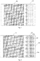
- the application first provides an array substrate, as shown in Fig.2 , and the array substrate includes a substrate 10, and a gate drive circuit 11 and a common electrode line 22 arranged above the substrate 10, wherein the gate drive circuit 11 and the common electrode line 22 are arranged adjacent to each other, and at least one groove 23 is provided in the common electrode line 22.
- the gate drive circuit 11 includes a large number of thin film transistors and connection lines, and these lines have a relatively large density.
- the existing common electrode line is generally designed to be a wide bulk metal, which will lead to a nonuniform distribution of the developing solution. The developing solution will readily spread to the gate drive circuit 11, which will result in a broken circuit in the thin film transistor of the gate drive circuit 11.
- a groove 23 is provided in the common electrode line which is a bulk of a large area.
- the groove 23 not only can consume a part of developing solution, but also can guide flow of the developing solution, so as to improve the distribution uniformity of the developing solution and avoid the phenomenon that local accumulation of the developing solution results in an abnormal broken line from occurring.
- the application can suppress the developing solution to flow from the common electrode line 22 to the gate drive circuit 11, so as to solve the problem that the channel is broken in the thin film transistor of the gate drive circuit 11 due to nonuniform distribution of the developing solution.
- the groove 23 passes through the common electrode line 22 in a thickness direction (i.e. a direction perpendicular to the array subs trate). That is, the groove 23 is formed to be a slit passing through the common electrode line 22 to further increase ability of the groove to guide flow of the developing solution. Moreover, the common electrode line is completely etched so as to make the groove 23 be a slit, which is also easily controlled in the process.
- Arrangement of the groove 23 is not limited in the application, and during a practical production, the groove is arranged such that the developing solution is distributed more uniformly.
- a plurality of grooves 23 are provided in the common electrode line 22, and the plurality of grooves 23 extend in a same direction.
- the plurality of grooves 23 are provided to reduce difference between the line density of the common electrode line 22 and that of the gate drive circuit 11 and increase distribution uniformity of the lines on the overall substrate, and thus the distribution of the developing solution is more uniform, and the production yield is increased.
- the plurality of grooves 23 pass through the common electrode line 22 in a thickness direction, the common electrode line 22 is segmented into a plurality of common electrode line strips 22a by the plurality of grooves 23, the common electrode line 22 further includes a connection part 22b, and the plurality of common electrode line strips 22a are electrically connected by the connection part 22b at one end of the common electrode line 22. That is, the common electrode line 22 in the application may be designed to be a structure like a comb.
- the gate drive circuit 11 shown in Fig. 2 includes multiple stages of shift register units which are cascaded, and each stage of shift register unit includes a plurality of thin film transistors.
- a source and a drain of the thin film transistor and the common electrode line 22 are provided in a same metal layer.
- the plurality of grooves 23 are provided in the common electrode line 22, the developing solution is prevented from flowing to a region of the gate drive circuit 11 in which the thin film transistors are densely distributed, and thus the problem that the channel between the source and the drain is broken in the thin film transistor of the gate drive circuit 11 due to high concentration of the local developing solution.
- the application further provides a method for manufacturing an array substrate, which includes a gat e drive circuit and a common electrode line which are arranged adjacent to each other and are arranged a bove a substrate, wherein the method includes steps of:
- a pattern of a source and a drain of a thin film transistor in the gate drive circuit is also formed while performing the etching process on the metal layer to form the pattern of the common electrode line.
- a mask pattern of the used mask plate corresponds to a metal pattern to be formed.
- a pattern of the common electrode line is improved, and the groove provided in the common electrode line can guide flow of the developing solution in the development process, so as to make the developing solution distribute uniformity on the surface of the metal layer and avoid the phenomenon that local accumulation of the developing solution due to the difference between line densities results in an abnormal broken line from occurring.
- the gate drive circuit and the common electrode line are arranged adjacent to each other, flow of the developing solution from the common electrode line to the gate drive circuit can be suppressed, so as to solve the problem that the channel is broken in the thin film transistor of the gate drive circuit due to nonuniform distribution of the developing solution.
- the groove passes through the common electrode line in a thickness direction, to further increase ability of the groove to guide flow of the developing solution.
- a plurality of grooves are provided in the common electrode line, and the plurality of grooves extend in a same direction.
- the plurality of grooves are provided to reduce difference between the line density of the common electrode line and that of the gate drive circuit and increase distribution uniformity of the lines on the overall substrate, and thus the distribution of the developing solution is more uniform, and the production yield is increased.
- the groove is not limited in the application, and during a practical production, the groove is arranged such that the developing solution is distributed more uniformly.
- the common electrode line may be formed to be a structure like a comb.
- the plurality of grooves 23 pass through the common electrode line 22 in a thickness direction, the common electrode line 22 is segmented into a plurality of common electrode line strips 22a by the plurality of grooves 23, the common electrode line 22 further includes a connection part 22b, and the plurality of common electrode line strips 22a are electrically connected by the connection part 22b at one end of the common electrode line 22.
- the application further provides a display device, which includes the above array substrate provided by the application.
- a display device which includes the above array substrate provided by the application.
Landscapes
- Physics & Mathematics (AREA)
- Nonlinear Science (AREA)
- General Physics & Mathematics (AREA)
- Chemical & Material Sciences (AREA)
- Crystallography & Structural Chemistry (AREA)
- Optics & Photonics (AREA)
- Mathematical Physics (AREA)
- Engineering & Computer Science (AREA)
- Computer Hardware Design (AREA)
- Theoretical Computer Science (AREA)
- Microelectronics & Electronic Packaging (AREA)
- Geometry (AREA)
- Liquid Crystal (AREA)
- Devices For Indicating Variable Information By Combining Individual Elements (AREA)
Abstract
Description
- The present application relates to the field of display technology, and in particular, relates to an array substrate and a method for manufacturing the same, and a display device including the array substrate.
- In a thin film transistor liquid crystal display panel (TFT-LCD), a gate drive circuit is generally integrated into an array substrate to form a GOA (Gate On Array) unit for achieving line scanning drive for a display panel.
- As shown in
Fig. 1 , agate drive circuit 11 is provided in the periphery of the display panel, thegate drive circuit 11 includes a large number of thin film transistors and lines, and density of the lines are relatively large. A common electrode line 12 (Vcom line) is provided near thegate drive circuit 11, and the existingcommon electrode line 12 is generally designed to be a wide bulk metal, which may lead to a large difference between the density of lines in thegate drive circuit 11 and the line density of thecommon electrode line 12. - When a patterning process is performed, the above difference will result in nonuniform local developing solution, the developing solution is not consumed in the region corresponding to the bulk metal, and the unconsumed developing solution will spread into the periphery of large line density, as the arrow in
Fig. 1 shown, which will result in a broken circuit in the thin filmtransistor of thegate drive circuit 11, and cause various display adverse phenomena to occur. - An object of the present application is to provide an array substrate and a method for manufacturing the same, and a display device including the array substrate, to solve the problem in the prior art that a broken circuit occurs in the thin film transistor of the gate drive circuit due to the nonuniform distribution of the developing solution when the array substrate is manufactured.
- To solve the above problem, as an aspect of the application, an array substrate is provided, and the array substrate includes a substrate, a gate drive circuit and a common electrode line arranged above the substrate, the gate drive circuit and the common electrode line are arranged adjacent to each other, and at least one groove is provided in the common electrode line.
- Optionally, the groove passes through the common electrode line in a direction perpendicular to the array substrate.
- Optionally, a plurality of grooves are provided in the common electrode line, and the plurality of grooves extend in a same direction.
- Optionally, the plurality of grooves pass through the common electrode line in a direction perpendicular to the array substrate, the common electrode line is segmented into a plurality of common electrode line strips by the plurality of grooves, the common electrode line further includes a connection part, and the plurality of common electrode line strips are electrically connected by the connection part at one end of the common electrode line.
- Optionally, the gate drive circuit includes multiple stages of shift register units which are cascaded, each stage of shift register unit includes a plurality of thin film transistors, and a source and a drain of the thin film transistor and the common electrode line are provided in a same metal layer.
- As a second aspect of the application, a method for manufacturing an array substrate is provided, and the array substrate includes a gate drive circuit and a common electrode line which are arranged adjacent to each ot her and are arranged above a substrate, wherein the method includes steps of:
- forming a metal layer above the substrate;
- forming a photoresist layer on the metal layer;
- performing exposure and development on the photoresist layer; and
- performing an etching process on the metal layer to form a pattern of the common electrode line such that at least one groove is formed in the common electrode line.
- Optionally, a pattern of a source and a drain of a thin film transistor in the gate drive circuit is also formed while performing the etching process on the metal layer to form the pattern of the common electrode line.
- Optionally, the groove passes through the common electrode line in a direction perpendicular to the array substrate.
- Optionally, a plurality of grooves are provided in the common electrode line, and the plurality of grooves extend in a same direction.
- Optionally, the plurality of grooves pass through the common electrode line in a direction perpendicular to the array substrate, the common electrode line is segmented into a plurality of common electrode line strips by the plurality of grooves, the common electrode line further includes a connection part, and the plurality of common electrode line strips are electrically connected by the connection part at one end of the common electrode line.
- As a third aspect of the application, a display device is provided, and the display device includes the above array substrate provided by the application.
- In the application, by forming the groove in the common electrode line, flow of the developing solution from the common electrode line to the gate drive circuit can be effectively suppressed, so as to solve the problem that the channel is broken in the thin film transistor of the gate drive circuit due to nonuniform distribution of the developing solution.
- The accompanying drawings are provided for further understanding of the present invention and constitute a part of the description. The accompanying drawings, together with the following embodiments, are provided for explaining the present invention rather than limiting the present invention. In the drawings:
-
Fig. 1 is a schematic view of an array substrate in the prior art; -
Figs. 2 is a schematic view of an array substrate according to an embodiment of the application; and -
Fig. 3 is a flow chart illustrating a method for manufacturing the thin film transistor according to an embodiment of the application. - 10-substrate; 11-gate drive circuit; 12, 22-common electrode line; 22a-common electrode line strip; 22b-connection part; 23-groove.
- Embodiments of the present application will be described in detail below with reference to the accompanying drawings . It should be noted that, the embodiments described herein are for the purpose of describing and explaining the present invention, rather than limiting the scope of the present invention.
- The application first provides an array substrate, as shown in
Fig.2 , and the array substrate includes asubstrate 10, and agate drive circuit 11 and acommon electrode line 22 arranged above thesubstrate 10, wherein thegate drive circuit 11 and thecommon electrode line 22 are arranged adjacent to each other, and at least onegroove 23 is provided in thecommon electrode line 22. - As described above, the
gate drive circuit 11 includes a large number of thin film transistors and connection lines, and these lines have a relatively large density. The existing common electrode line is generally designed to be a wide bulk metal, which will lead to a nonuniform distribution of the developing solution. The developing solution will readily spread to thegate drive circuit 11, which will result in a broken circuit in the thin film transistor of thegate drive circuit 11. - Compared to the prior art, in the application, a
groove 23 is provided in the common electrode line which is a bulk of a large area. During a pattering process, thegroove 23 not only can consume a part of developing solution, but also can guide flow of the developing solution, so as to improve the distribution uniformity of the developing solution and avoid the phenomenon that local accumulation of the developing solution results in an abnormal broken line from occurring. - In particular, the application can suppress the developing solution to flow from the
common electrode line 22 to thegate drive circuit 11, so as to solve the problem that the channel is broken in the thin film transistor of thegate drive circuit 11 due to nonuniform distribution of the developing solution. - Optionally, the
groove 23 passes through thecommon electrode line 22 in a thickness direction (i.e. a direction perpendicular to the array subs trate). That is, thegroove 23 is formed to be a slit passing through thecommon electrode line 22 to further increase ability of the groove to guide flow of the developing solution. Moreover, the common electrode line is completely etched so as to make thegroove 23 be a slit, which is also easily controlled in the process. - Arrangement of the
groove 23 is not limited in the application, and during a practical production, the groove is arranged such that the developing solution is distributed more uniformly. - As a preferable embodiment of the application, as shown in
Fig. 2 , a plurality ofgrooves 23 are provided in thecommon electrode line 22, and the plurality ofgrooves 23 extend in a same direction. The plurality ofgrooves 23 are provided to reduce difference between the line density of thecommon electrode line 22 and that of thegate drive circuit 11 and increase distribution uniformity of the lines on the overall substrate, and thus the distribution of the developing solution is more uniform, and the production yield is increased. - Further, the plurality of
grooves 23 pass through thecommon electrode line 22 in a thickness direction, thecommon electrode line 22 is segmented into a plurality of commonelectrode line strips 22a by the plurality ofgrooves 23, thecommon electrode line 22 further includes aconnection part 22b, and the plurality of commonelectrode line strips 22a are electrically connected by theconnection part 22b at one end of thecommon electrode line 22. That is, thecommon electrode line 22 in the application may be designed to be a structure like a comb. - Generally, the
gate drive circuit 11 shown inFig. 2 includes multiple stages of shift register units which are cascaded, and each stage of shift register unit includes a plurality of thin film transistors. In the application, a source and a drain of the thin film transistor and thecommon electrode line 22 are provided in a same metal layer. During forming a pattern of the metal layer, since the plurality ofgrooves 23 are provided in thecommon electrode line 22, the developing solution is prevented from flowing to a region of thegate drive circuit 11 in which the thin film transistors are densely distributed, and thus the problem that the channel between the source and the drain is broken in the thin film transistor of thegate drive circuit 11 due to high concentration of the local developing solution. - As shown in
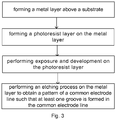
Fig. 3 , the application further provides a method for manufacturing an array substrate, which includes a gat e drive circuit and a common electrode line which are arranged adjacent to each other and are arranged a bove a substrate, wherein the method includes steps of: - forming a metal layer above the substrate;
- forming a photoresist layer on the metal layer;
- performing exposure and development on the photoresist layer; and
- performing an etching process on the metal layer to form a pattern of the common electrode line such that at least one groove is formed in the common electrode line.
- Optionally, a pattern of a source and a drain of a thin film transistor in the gate drive circuit is also formed while performing the etching process on the metal layer to form the pattern of the common electrode line.
- It should be understood that, when performing exposure and development on the photoresist layer, a mask pattern of the used mask plate corresponds to a metal pattern to be formed.
- In the method for manufacturing an array substrate in the application, a pattern of the common electrode line is improved, and the groove provided in the common electrode line can guide flow of the developing solution in the development process, so as to make the developing solution distribute uniformity on the surface of the metal layer and avoid the phenomenon that local accumulation of the developing solution due to the difference between line densities results in an abnormal broken line from occurring.
- In the embodiment of the application, since the gate drive circuit and the common electrode line are arranged adjacent to each other, flow of the developing solution from the common electrode line to the gate drive circuit can be suppressed, so as to solve the problem that the channel is broken in the thin film transistor of the gate drive circuit due to nonuniform distribution of the developing solution.
- Optionally, the groove passes through the common electrode line in a thickness direction, to further increase ability of the groove to guide flow of the developing solution.
- Further, a plurality of grooves are provided in the common electrode line, and the plurality of grooves extend in a same direction. The plurality of grooves are provided to reduce difference between the line density of the common electrode line and that of the gate drive circuit and increase distribution uniformity of the lines on the overall substrate, and thus the distribution of the developing solution is more uniform, and the production yield is increased.
- Arrangement of the groove is not limited in the application, and during a practical production, the groove is arranged such that the developing solution is distributed more uniformly.
- For example, the common electrode line may be formed to be a structure like a comb. As shown in
Fig. 2 , the plurality ofgrooves 23 pass through thecommon electrode line 22 in a thickness direction, thecommon electrode line 22 is segmented into a plurality of common electrode line strips 22a by the plurality ofgrooves 23, thecommon electrode line 22 further includes aconnection part 22b, and the plurality of common electrode line strips 22a are electrically connected by theconnection part 22b at one end of thecommon electrode line 22. - The application further provides a display device, which includes the above array substrate provided by the application. As described above, in the display device provided by the application, since the lines are distributed more uniformly, the developing solution is distributed more uniformly during the manufacturing process, the phenomenon that local accumulation of the developing solution results in an abnormal broken line can be effectively avoided from occurring, and thus a production yield is increased.
- It should be understood that, the above embodiments are only exemplary embodiments for the purpose of explaining the principle of the present application, but the present application is not limited thereto. For a person having ordinary skill in the art, various improvements and modifications may be made without departing from the spirit and essence of the present application. These improvements and modifications also fall within the protection scope of the present application.
Claims (11)
- An array substrate, including a substrate, and a gate drive circuit and a common electrode line arranged above the substrate, wherein the gate drive circuit and the common electrode line are arranged adjacent to each other, and at least one groove is provided in the common electrode line.
- The array substrate of claim 1, wherein the groove passes through the common electrode line in a direction perpendicular to the array substrate.
- The array substrate of claim 1, wherein a plurality of grooves are provided in the common electrode line, and the plurality of grooves extend in a same direction.
- The array substrate of claim 3, wherein the plurality of grooves pass through the common electrode line in a direction perpendicular to the array substrate, the common electrode line is segmented into a plurality of common electrode line strips by the plurality of grooves, the common electrode line further includes a connection part, and the plurality of common electrode line strips are electrically connected by the connection part at one end of the common electrode line.
- The array substrate of any one of claims 1 to 4, wherein the gate drive circuit includes multiple stages of shift register units which are cascaded, each stage of shift register unit includes a plurality of thin film transistors, and a source and a drain of the thin film transistor and the common electrode line are provided in a same metal layer.
- A method for manufacturing an array substrate, which includes a gate drive circuit and a common electrode line which are arranged adjacent to each other and are arranged above a substrate, wherein the method includes steps of:forming a metal layer above the substrate;forming a photoresist layer on the metal layer;performing exposure and development on the photoresist layer; andperforming an etching process on the metal layer to form a pattern of the common electrode line such that at least one groove is formed in the common electrode line.
- The method of claim 6, wherein a pattern of a source and a drain of a thin film transistor in the gate drive circuit is also formed while performing the etching process on the metal layer to form the pattern of the common electrode line.
- The method of claim 6 or 7, wherein the groove passes through the common electrode line in a direction perpendicular to the array substrate.
- The method of claim 6 or 7, wherein a plurality of grooves are provided in the common electrode line, and the plurality of grooves extend in a same direction.
- The method of claim 9, wherein the plurality of grooves pass through the common electrode line in a direction perpendicular to the array substrate, the common electrode line is segmented into a plurality of common electrode line strips by the plurality of grooves, the common electrode line further includes a connection part, and the plurality of common electrode line strips are electrically connected by the connection part at one end of the common electrode line.
- A display device, including the array substrate of any one of claims 1 to 5.
Applications Claiming Priority (2)
| Application Number | Priority Date | Filing Date | Title |
|---|---|---|---|
| CN201510561375.XA CN105261621B (en) | 2015-09-06 | 2015-09-06 | Array base palte and preparation method thereof, display device |
| PCT/CN2016/077320 WO2017036123A1 (en) | 2015-09-06 | 2016-03-25 | Array substrate, and manufacturing method and display device therefor |
Publications (3)
| Publication Number | Publication Date |
|---|---|
| EP3346495A1 true EP3346495A1 (en) | 2018-07-11 |
| EP3346495A4 EP3346495A4 (en) | 2019-04-10 |
| EP3346495B1 EP3346495B1 (en) | 2021-10-27 |
Family
ID=55101231
Family Applications (1)
| Application Number | Title | Priority Date | Filing Date |
|---|---|---|---|
| EP16818968.6A Active EP3346495B1 (en) | 2015-09-06 | 2016-03-25 | Array substrate, and manufacturing method and display device therefor |
Country Status (4)
| Country | Link |
|---|---|
| US (1) | US10809580B2 (en) |
| EP (1) | EP3346495B1 (en) |
| CN (1) | CN105261621B (en) |
| WO (1) | WO2017036123A1 (en) |
Families Citing this family (2)
| Publication number | Priority date | Publication date | Assignee | Title |
|---|---|---|---|---|
| CN105261621B (en) | 2015-09-06 | 2018-01-30 | 京东方科技集团股份有限公司 | Array base palte and preparation method thereof, display device |
| CN111640766B (en) * | 2020-06-22 | 2023-12-12 | 武汉华星光电技术有限公司 | Array substrate and manufacturing method thereof |
Family Cites Families (14)
| Publication number | Priority date | Publication date | Assignee | Title |
|---|---|---|---|---|
| JP4449953B2 (en) * | 2006-07-27 | 2010-04-14 | エプソンイメージングデバイス株式会社 | Liquid crystal display |
| US8035662B2 (en) * | 2006-11-22 | 2011-10-11 | Seiko Epson Corporation | Integrated circuit device and electronic instrument |
| EP2565877A4 (en) * | 2010-04-28 | 2013-07-10 | Sharp Kk | SHIFT REGISTER AND DISPLAY DEVICE |
| KR101242033B1 (en) * | 2010-05-05 | 2013-03-11 | 엘지디스플레이 주식회사 | Array substrate for liquid crystal display device and method of fabricating the same |
| KR101720524B1 (en) * | 2010-06-07 | 2017-03-28 | 엘지디스플레이 주식회사 | Liquid Crystal Display Device and Method for manufacturing the same |
| CN102280436B (en) * | 2010-06-09 | 2014-08-06 | 北京京东方光电科技有限公司 | Thin film metal layer wiring structure and manufacturing method thereof, and array substrate |
| CN102466936B (en) * | 2010-11-04 | 2014-02-19 | 京东方科技集团股份有限公司 | Array substrate, liquid crystal display and manufacturing method of array substrate |
| CN102645803B (en) * | 2011-10-17 | 2014-06-18 | 京东方科技集团股份有限公司 | Pixel unit, array substrate, liquid crystal panel, display device and manufacturing methods thereof |
| US9412799B2 (en) * | 2013-08-26 | 2016-08-09 | Apple Inc. | Display driver circuitry for liquid crystal displays with semiconducting-oxide thin-film transistors |
| CN104090436B (en) * | 2014-06-26 | 2017-03-22 | 京东方科技集团股份有限公司 | Gate line drive circuit of array substrate and display device |
| CN104238214B (en) * | 2014-07-24 | 2017-02-15 | 京东方科技集团股份有限公司 | Array substrate and display panel |
| CN104483768B (en) * | 2015-01-04 | 2017-07-04 | 京东方科技集团股份有限公司 | Display panel and preparation method thereof and display device |
| CN104538412A (en) | 2015-01-26 | 2015-04-22 | 京东方科技集团股份有限公司 | Array substrate and production method thereof and display device |
| CN105261621B (en) | 2015-09-06 | 2018-01-30 | 京东方科技集团股份有限公司 | Array base palte and preparation method thereof, display device |
-
2015
- 2015-09-06 CN CN201510561375.XA patent/CN105261621B/en active Active
-
2016
- 2016-03-25 EP EP16818968.6A patent/EP3346495B1/en active Active
- 2016-03-25 US US15/324,405 patent/US10809580B2/en active Active
- 2016-03-25 WO PCT/CN2016/077320 patent/WO2017036123A1/en not_active Ceased
Also Published As
| Publication number | Publication date |
|---|---|
| CN105261621B (en) | 2018-01-30 |
| CN105261621A (en) | 2016-01-20 |
| WO2017036123A1 (en) | 2017-03-09 |
| US20170199413A1 (en) | 2017-07-13 |
| US10809580B2 (en) | 2020-10-20 |
| EP3346495A4 (en) | 2019-04-10 |
| EP3346495B1 (en) | 2021-10-27 |
Similar Documents
| Publication | Publication Date | Title |
|---|---|---|
| US10001686B2 (en) | Array substrate and fabrication method thereof, and display device | |
| US10539836B2 (en) | Display substrate, method of fabricating the same, and display device | |
| US11467456B2 (en) | Array substrate, display panel and display apparatus | |
| KR20060065978A (en) | Slit mask | |
| US20120092607A1 (en) | Pixel electrode layer structure of tft-lcd, method for manufacturing the same and mask therefor | |
| US9508867B2 (en) | Thin film transistor, array substrate, method of fabricating same, and display device | |
| CN101382728B (en) | Gray scale mask structure | |
| CN105974620A (en) | Method for manufacturing substrate, substrate and display device | |
| US9923040B2 (en) | Array substrate and display device | |
| WO2020248701A1 (en) | Array substrate, display panel and display device | |
| US10608021B2 (en) | TFT substrate manufacturing method and TFT substrate | |
| US10256260B2 (en) | Display substrate, manufacturing method therefor and display device | |
| CN104932159A (en) | Display substrate, manufacturing method of display substrate, driving method and display device | |
| US11398539B2 (en) | Array substrate, display panel and display device | |
| CN104199209A (en) | Mask plate, manufacturing method thereof and manufacturing method of target graph | |
| EP3346495A1 (en) | Array substrate, and manufacturing method and display device therefor | |
| CN102983102B (en) | Array substrate and manufacturing method thereof, as well as display device | |
| US10243007B2 (en) | Array substrate and manufacturing method thereof, display panel and display device | |
| CN105185839B (en) | TFT and its manufacturing method, driving circuit and display device | |
| CN105390505B (en) | Thin-film transistor array base-plate and preparation method thereof | |
| CN106054516A (en) | Mask, array substrate, manufacturing method of array substrate and display device | |
| US10153309B2 (en) | Manufacturing method of display panel | |
| CN104112710A (en) | Manufacturing method of array substrates, array substrates and liquid crystal display device | |
| US9746734B2 (en) | Pixel structure and manufacturing method thereof, display panel and display device | |
| US10692895B2 (en) | Array substrates, display panels, and display apparatuses |
Legal Events
| Date | Code | Title | Description |
|---|---|---|---|
| STAA | Information on the status of an ep patent application or granted ep patent |
Free format text: STATUS: UNKNOWN |
|
| STAA | Information on the status of an ep patent application or granted ep patent |
Free format text: STATUS: THE INTERNATIONAL PUBLICATION HAS BEEN MADE |
|
| PUAI | Public reference made under article 153(3) epc to a published international application that has entered the european phase |
Free format text: ORIGINAL CODE: 0009012 |
|
| STAA | Information on the status of an ep patent application or granted ep patent |
Free format text: STATUS: REQUEST FOR EXAMINATION WAS MADE |
|
| 17P | Request for examination filed |
Effective date: 20170106 |
|
| AK | Designated contracting states |
Kind code of ref document: A1 Designated state(s): AL AT BE BG CH CY CZ DE DK EE ES FI FR GB GR HR HU IE IS IT LI LT LU LV MC MK MT NL NO PL PT RO RS SE SI SK SM TR |
|
| AX | Request for extension of the european patent |
Extension state: BA ME |
|
| DAV | Request for validation of the european patent (deleted) | ||
| DAX | Request for extension of the european patent (deleted) | ||
| A4 | Supplementary search report drawn up and despatched |
Effective date: 20190307 |
|
| RIC1 | Information provided on ipc code assigned before grant |
Ipc: H01L 27/12 20060101AFI20190301BHEP Ipc: G02F 1/1345 20060101ALI20190301BHEP |
|
| GRAP | Despatch of communication of intention to grant a patent |
Free format text: ORIGINAL CODE: EPIDOSNIGR1 |
|
| STAA | Information on the status of an ep patent application or granted ep patent |
Free format text: STATUS: GRANT OF PATENT IS INTENDED |
|
| INTG | Intention to grant announced |
Effective date: 20210511 |
|
| GRAS | Grant fee paid |
Free format text: ORIGINAL CODE: EPIDOSNIGR3 |
|
| GRAA | (expected) grant |
Free format text: ORIGINAL CODE: 0009210 |
|
| STAA | Information on the status of an ep patent application or granted ep patent |
Free format text: STATUS: THE PATENT HAS BEEN GRANTED |
|
| AK | Designated contracting states |
Kind code of ref document: B1 Designated state(s): AL AT BE BG CH CY CZ DE DK EE ES FI FR GB GR HR HU IE IS IT LI LT LU LV MC MK MT NL NO PL PT RO RS SE SI SK SM TR |
|
| REG | Reference to a national code |
Ref country code: GB Ref legal event code: FG4D |
|
| REG | Reference to a national code |
Ref country code: CH Ref legal event code: EP |
|
| REG | Reference to a national code |
Ref country code: AT Ref legal event code: REF Ref document number: 1442610 Country of ref document: AT Kind code of ref document: T Effective date: 20211115 |
|
| REG | Reference to a national code |
Ref country code: DE Ref legal event code: R096 Ref document number: 602016065499 Country of ref document: DE |
|
| REG | Reference to a national code |
Ref country code: IE Ref legal event code: FG4D |
|
| REG | Reference to a national code |
Ref country code: LT Ref legal event code: MG9D |
|
| REG | Reference to a national code |
Ref country code: NL Ref legal event code: MP Effective date: 20211027 |
|
| REG | Reference to a national code |
Ref country code: AT Ref legal event code: MK05 Ref document number: 1442610 Country of ref document: AT Kind code of ref document: T Effective date: 20211027 |
|
| PG25 | Lapsed in a contracting state [announced via postgrant information from national office to epo] |
Ref country code: RS Free format text: LAPSE BECAUSE OF FAILURE TO SUBMIT A TRANSLATION OF THE DESCRIPTION OR TO PAY THE FEE WITHIN THE PRESCRIBED TIME-LIMIT Effective date: 20211027 Ref country code: LT Free format text: LAPSE BECAUSE OF FAILURE TO SUBMIT A TRANSLATION OF THE DESCRIPTION OR TO PAY THE FEE WITHIN THE PRESCRIBED TIME-LIMIT Effective date: 20211027 Ref country code: FI Free format text: LAPSE BECAUSE OF FAILURE TO SUBMIT A TRANSLATION OF THE DESCRIPTION OR TO PAY THE FEE WITHIN THE PRESCRIBED TIME-LIMIT Effective date: 20211027 Ref country code: BG Free format text: LAPSE BECAUSE OF FAILURE TO SUBMIT A TRANSLATION OF THE DESCRIPTION OR TO PAY THE FEE WITHIN THE PRESCRIBED TIME-LIMIT Effective date: 20220127 Ref country code: AT Free format text: LAPSE BECAUSE OF FAILURE TO SUBMIT A TRANSLATION OF THE DESCRIPTION OR TO PAY THE FEE WITHIN THE PRESCRIBED TIME-LIMIT Effective date: 20211027 |
|
| PG25 | Lapsed in a contracting state [announced via postgrant information from national office to epo] |
Ref country code: IS Free format text: LAPSE BECAUSE OF FAILURE TO SUBMIT A TRANSLATION OF THE DESCRIPTION OR TO PAY THE FEE WITHIN THE PRESCRIBED TIME-LIMIT Effective date: 20220227 Ref country code: SE Free format text: LAPSE BECAUSE OF FAILURE TO SUBMIT A TRANSLATION OF THE DESCRIPTION OR TO PAY THE FEE WITHIN THE PRESCRIBED TIME-LIMIT Effective date: 20211027 Ref country code: PT Free format text: LAPSE BECAUSE OF FAILURE TO SUBMIT A TRANSLATION OF THE DESCRIPTION OR TO PAY THE FEE WITHIN THE PRESCRIBED TIME-LIMIT Effective date: 20220228 Ref country code: PL Free format text: LAPSE BECAUSE OF FAILURE TO SUBMIT A TRANSLATION OF THE DESCRIPTION OR TO PAY THE FEE WITHIN THE PRESCRIBED TIME-LIMIT Effective date: 20211027 Ref country code: NO Free format text: LAPSE BECAUSE OF FAILURE TO SUBMIT A TRANSLATION OF THE DESCRIPTION OR TO PAY THE FEE WITHIN THE PRESCRIBED TIME-LIMIT Effective date: 20220127 Ref country code: NL Free format text: LAPSE BECAUSE OF FAILURE TO SUBMIT A TRANSLATION OF THE DESCRIPTION OR TO PAY THE FEE WITHIN THE PRESCRIBED TIME-LIMIT Effective date: 20211027 Ref country code: LV Free format text: LAPSE BECAUSE OF FAILURE TO SUBMIT A TRANSLATION OF THE DESCRIPTION OR TO PAY THE FEE WITHIN THE PRESCRIBED TIME-LIMIT Effective date: 20211027 Ref country code: HR Free format text: LAPSE BECAUSE OF FAILURE TO SUBMIT A TRANSLATION OF THE DESCRIPTION OR TO PAY THE FEE WITHIN THE PRESCRIBED TIME-LIMIT Effective date: 20211027 Ref country code: GR Free format text: LAPSE BECAUSE OF FAILURE TO SUBMIT A TRANSLATION OF THE DESCRIPTION OR TO PAY THE FEE WITHIN THE PRESCRIBED TIME-LIMIT Effective date: 20220128 Ref country code: ES Free format text: LAPSE BECAUSE OF FAILURE TO SUBMIT A TRANSLATION OF THE DESCRIPTION OR TO PAY THE FEE WITHIN THE PRESCRIBED TIME-LIMIT Effective date: 20211027 |
|
| REG | Reference to a national code |
Ref country code: DE Ref legal event code: R097 Ref document number: 602016065499 Country of ref document: DE |
|
| PG25 | Lapsed in a contracting state [announced via postgrant information from national office to epo] |
Ref country code: SM Free format text: LAPSE BECAUSE OF FAILURE TO SUBMIT A TRANSLATION OF THE DESCRIPTION OR TO PAY THE FEE WITHIN THE PRESCRIBED TIME-LIMIT Effective date: 20211027 Ref country code: SK Free format text: LAPSE BECAUSE OF FAILURE TO SUBMIT A TRANSLATION OF THE DESCRIPTION OR TO PAY THE FEE WITHIN THE PRESCRIBED TIME-LIMIT Effective date: 20211027 Ref country code: RO Free format text: LAPSE BECAUSE OF FAILURE TO SUBMIT A TRANSLATION OF THE DESCRIPTION OR TO PAY THE FEE WITHIN THE PRESCRIBED TIME-LIMIT Effective date: 20211027 Ref country code: EE Free format text: LAPSE BECAUSE OF FAILURE TO SUBMIT A TRANSLATION OF THE DESCRIPTION OR TO PAY THE FEE WITHIN THE PRESCRIBED TIME-LIMIT Effective date: 20211027 Ref country code: DK Free format text: LAPSE BECAUSE OF FAILURE TO SUBMIT A TRANSLATION OF THE DESCRIPTION OR TO PAY THE FEE WITHIN THE PRESCRIBED TIME-LIMIT Effective date: 20211027 Ref country code: CZ Free format text: LAPSE BECAUSE OF FAILURE TO SUBMIT A TRANSLATION OF THE DESCRIPTION OR TO PAY THE FEE WITHIN THE PRESCRIBED TIME-LIMIT Effective date: 20211027 |
|
| PLBE | No opposition filed within time limit |
Free format text: ORIGINAL CODE: 0009261 |
|
| STAA | Information on the status of an ep patent application or granted ep patent |
Free format text: STATUS: NO OPPOSITION FILED WITHIN TIME LIMIT |
|
| 26N | No opposition filed |
Effective date: 20220728 |
|
| PG25 | Lapsed in a contracting state [announced via postgrant information from national office to epo] |
Ref country code: MC Free format text: LAPSE BECAUSE OF FAILURE TO SUBMIT A TRANSLATION OF THE DESCRIPTION OR TO PAY THE FEE WITHIN THE PRESCRIBED TIME-LIMIT Effective date: 20211027 Ref country code: AL Free format text: LAPSE BECAUSE OF FAILURE TO SUBMIT A TRANSLATION OF THE DESCRIPTION OR TO PAY THE FEE WITHIN THE PRESCRIBED TIME-LIMIT Effective date: 20211027 |
|
| REG | Reference to a national code |
Ref country code: CH Ref legal event code: PL |
|
| PG25 | Lapsed in a contracting state [announced via postgrant information from national office to epo] |
Ref country code: SI Free format text: LAPSE BECAUSE OF FAILURE TO SUBMIT A TRANSLATION OF THE DESCRIPTION OR TO PAY THE FEE WITHIN THE PRESCRIBED TIME-LIMIT Effective date: 20211027 |
|
| REG | Reference to a national code |
Ref country code: BE Ref legal event code: MM Effective date: 20220331 |
|
| PG25 | Lapsed in a contracting state [announced via postgrant information from national office to epo] |
Ref country code: LU Free format text: LAPSE BECAUSE OF NON-PAYMENT OF DUE FEES Effective date: 20220325 Ref country code: LI Free format text: LAPSE BECAUSE OF NON-PAYMENT OF DUE FEES Effective date: 20220331 Ref country code: IE Free format text: LAPSE BECAUSE OF NON-PAYMENT OF DUE FEES Effective date: 20220325 Ref country code: CH Free format text: LAPSE BECAUSE OF NON-PAYMENT OF DUE FEES Effective date: 20220331 |
|
| PG25 | Lapsed in a contracting state [announced via postgrant information from national office to epo] |
Ref country code: BE Free format text: LAPSE BECAUSE OF NON-PAYMENT OF DUE FEES Effective date: 20220331 |
|
| PG25 | Lapsed in a contracting state [announced via postgrant information from national office to epo] |
Ref country code: IT Free format text: LAPSE BECAUSE OF FAILURE TO SUBMIT A TRANSLATION OF THE DESCRIPTION OR TO PAY THE FEE WITHIN THE PRESCRIBED TIME-LIMIT Effective date: 20211027 |
|
| PG25 | Lapsed in a contracting state [announced via postgrant information from national office to epo] |
Ref country code: HU Free format text: LAPSE BECAUSE OF FAILURE TO SUBMIT A TRANSLATION OF THE DESCRIPTION OR TO PAY THE FEE WITHIN THE PRESCRIBED TIME-LIMIT; INVALID AB INITIO Effective date: 20160325 |
|
| PG25 | Lapsed in a contracting state [announced via postgrant information from national office to epo] |
Ref country code: MK Free format text: LAPSE BECAUSE OF FAILURE TO SUBMIT A TRANSLATION OF THE DESCRIPTION OR TO PAY THE FEE WITHIN THE PRESCRIBED TIME-LIMIT Effective date: 20211027 Ref country code: CY Free format text: LAPSE BECAUSE OF FAILURE TO SUBMIT A TRANSLATION OF THE DESCRIPTION OR TO PAY THE FEE WITHIN THE PRESCRIBED TIME-LIMIT Effective date: 20211027 |
|
| PG25 | Lapsed in a contracting state [announced via postgrant information from national office to epo] |
Ref country code: TR Free format text: LAPSE BECAUSE OF FAILURE TO SUBMIT A TRANSLATION OF THE DESCRIPTION OR TO PAY THE FEE WITHIN THE PRESCRIBED TIME-LIMIT Effective date: 20211027 |
|
| PG25 | Lapsed in a contracting state [announced via postgrant information from national office to epo] |
Ref country code: MT Free format text: LAPSE BECAUSE OF FAILURE TO SUBMIT A TRANSLATION OF THE DESCRIPTION OR TO PAY THE FEE WITHIN THE PRESCRIBED TIME-LIMIT Effective date: 20211027 |
|
| REG | Reference to a national code |
Ref country code: DE Ref legal event code: R079 Ref document number: 602016065499 Country of ref document: DE Free format text: PREVIOUS MAIN CLASS: H01L0027120000 Ipc: H10D0086000000 |
|
| PGFP | Annual fee paid to national office [announced via postgrant information from national office to epo] |
Ref country code: GB Payment date: 20260324 Year of fee payment: 11 |
|
| PGFP | Annual fee paid to national office [announced via postgrant information from national office to epo] |
Ref country code: DE Payment date: 20260319 Year of fee payment: 11 |
|
| PGFP | Annual fee paid to national office [announced via postgrant information from national office to epo] |
Ref country code: FR Payment date: 20260320 Year of fee payment: 11 |