EP3346312A1 - Optical scanning module and optical scanning control device - Google Patents
Optical scanning module and optical scanning control device Download PDFInfo
- Publication number
- EP3346312A1 EP3346312A1 EP16850458.7A EP16850458A EP3346312A1 EP 3346312 A1 EP3346312 A1 EP 3346312A1 EP 16850458 A EP16850458 A EP 16850458A EP 3346312 A1 EP3346312 A1 EP 3346312A1
- Authority
- EP
- European Patent Office
- Prior art keywords
- interconnect
- optical scanner
- sensor
- package
- drive
- Prior art date
- Legal status (The legal status is an assumption and is not a legal conclusion. Google has not performed a legal analysis and makes no representation as to the accuracy of the status listed.)
- Granted
Links
Images






Classifications
-
- B—PERFORMING OPERATIONS; TRANSPORTING
- B81—MICROSTRUCTURAL TECHNOLOGY
- B81B—MICROSTRUCTURAL DEVICES OR SYSTEMS, e.g. MICROMECHANICAL DEVICES
- B81B7/00—Microstructural systems ; Auxiliary parts of microstructural devices or systems
- B81B7/0006—Interconnects
-
- B—PERFORMING OPERATIONS; TRANSPORTING
- B81—MICROSTRUCTURAL TECHNOLOGY
- B81B—MICROSTRUCTURAL DEVICES OR SYSTEMS, e.g. MICROMECHANICAL DEVICES
- B81B7/00—Microstructural systems ; Auxiliary parts of microstructural devices or systems
- B81B7/02—Microstructural systems ; Auxiliary parts of microstructural devices or systems containing distinct electrical or optical devices of particular relevance for their function, e.g. microelectro-mechanical systems [MEMS]
-
- G—PHYSICS
- G02—OPTICS
- G02B—OPTICAL ELEMENTS, SYSTEMS OR APPARATUS
- G02B26/00—Optical devices or arrangements for the control of light using movable or deformable optical elements
- G02B26/08—Optical devices or arrangements for the control of light using movable or deformable optical elements for controlling the direction of light
-
- G—PHYSICS
- G02—OPTICS
- G02B—OPTICAL ELEMENTS, SYSTEMS OR APPARATUS
- G02B26/00—Optical devices or arrangements for the control of light using movable or deformable optical elements
- G02B26/08—Optical devices or arrangements for the control of light using movable or deformable optical elements for controlling the direction of light
- G02B26/0816—Optical devices or arrangements for the control of light using movable or deformable optical elements for controlling the direction of light by means of one or more reflecting elements
- G02B26/0833—Optical devices or arrangements for the control of light using movable or deformable optical elements for controlling the direction of light by means of one or more reflecting elements the reflecting element being a micromechanical device, e.g. a MEMS mirror, DMD
- G02B26/0858—Optical devices or arrangements for the control of light using movable or deformable optical elements for controlling the direction of light by means of one or more reflecting elements the reflecting element being a micromechanical device, e.g. a MEMS mirror, DMD the reflecting means being moved or deformed by piezoelectric means
-
- G—PHYSICS
- G02—OPTICS
- G02B—OPTICAL ELEMENTS, SYSTEMS OR APPARATUS
- G02B26/00—Optical devices or arrangements for the control of light using movable or deformable optical elements
- G02B26/08—Optical devices or arrangements for the control of light using movable or deformable optical elements for controlling the direction of light
- G02B26/10—Scanning systems
-
- G—PHYSICS
- G02—OPTICS
- G02B—OPTICAL ELEMENTS, SYSTEMS OR APPARATUS
- G02B26/00—Optical devices or arrangements for the control of light using movable or deformable optical elements
- G02B26/08—Optical devices or arrangements for the control of light using movable or deformable optical elements for controlling the direction of light
- G02B26/10—Scanning systems
- G02B26/101—Scanning systems with both horizontal and vertical deflecting means, e.g. raster or XY scanners
-
- B—PERFORMING OPERATIONS; TRANSPORTING
- B81—MICROSTRUCTURAL TECHNOLOGY
- B81B—MICROSTRUCTURAL DEVICES OR SYSTEMS, e.g. MICROMECHANICAL DEVICES
- B81B2201/00—Specific applications of microelectromechanical systems
- B81B2201/04—Optical MEMS
- B81B2201/042—Micromirrors, not used as optical switches
-
- B—PERFORMING OPERATIONS; TRANSPORTING
- B81—MICROSTRUCTURAL TECHNOLOGY
- B81B—MICROSTRUCTURAL DEVICES OR SYSTEMS, e.g. MICROMECHANICAL DEVICES
- B81B2207/00—Microstructural systems or auxiliary parts thereof
- B81B2207/07—Interconnects
-
- B—PERFORMING OPERATIONS; TRANSPORTING
- B81—MICROSTRUCTURAL TECHNOLOGY
- B81B—MICROSTRUCTURAL DEVICES OR SYSTEMS, e.g. MICROMECHANICAL DEVICES
- B81B2207/00—Microstructural systems or auxiliary parts thereof
- B81B2207/09—Packages
- B81B2207/091—Arrangements for connecting external electrical signals to mechanical structures inside the package
- B81B2207/098—Arrangements not provided for in groups B81B2207/092 - B81B2207/097
Definitions
- the present invention relates to an optical scanner module and an optical scanner control apparatus.
- an optical scanner module in which an optical scanner apparatus that rotates a mirror around a rotation axis to reflect incident light such as laser light is mounted on a package.
- a displacement sensor that detects an oscillation angle of the mirror under a status that the mirror is driven and oscillated is provided, inclination of the mirror is detected based on a signal output from the displacement sensor, and the mirror is controlled to be driven (see Patent Document 1, for example).
- Patent Document 1 Japanese Laid-open Patent Publication No. 2014-235316
- a sensor interconnect connected to the displacement sensor and a drive interconnect through which a drive signal for oscillating the mirror passes may be drawn in the package in a complicated manner in the above described optical scanner module. Then, depending on a way of drawing the interconnects, cross-talk may be generated between the sensor interconnect and the drive interconnect, and there is a risk that a signal from the sensor interconnect cannot be accurately detected.
- the present invention is made in light of the above problems, and provides an optical scanner module capable of reducing cross-talk generated between a sensor interconnect and a drive interconnect.
- An optical scanner module (400) includes an optical scanner apparatus (30) that scans incident light by oscillating a mirror (310); and a package (410) on which the optical scanner apparatus (30) is mounted, wherein the optical scanner apparatus (30) includes a displacement sensor (391, 395, 396) that detects an oscillation angle of the mirror (310), wherein a sensor interconnect (P S ) connected to the displacement sensor (391, 395, 396) and a drive interconnect (P D ) through which a drive signal for oscillating the mirror (310) passes are respectively drawn from the optical scanner apparatus (30) into the package (410), wherein interconnect layers in which the sensor interconnect (P S ) and the drive interconnect (P D ) are formed are stacked, wherein the sensor interconnect (P S ) and the drive interconnect (P D ) are placed not to overlap in a plan view of the interconnect layers, and wherein a GND interconnect (P G ) is provided between the sensor interconnect (P S ) and the drive interconnect (P D ) that are
- an optical scanner module capable of reducing cross-talk generated between a sensor interconnect and a drive interconnect can be provided.
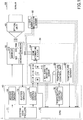
- Fig. 1 is a block diagram illustrating an example of an optical scanner control apparatus of a first embodiment.
- Fig. 2 is a plan view illustrating an example of an optical scanner apparatus that constitutes the optical scanner control apparatus.
- the optical scanner control apparatus 1 includes, as main constituents, a circuit unit 10, a light source unit 20, an optical scanner apparatus 30, an optical unit 40, a screen 50 and a light quantity detection sensor 60.
- the optical scanner control apparatus 1 is, for example, a laser scanning projector.
- the circuit unit 10 is a portion that controls the light source unit 20 and the optical scanner apparatus 30, and may be constituted by, for example, a system controller 11, a CPU (Central Processing Unit) 12, various driving circuits such as a buffer circuit 13, a mirror driving circuit 14, a laser driving circuit 15 and a temperature control circuit 16, and the like.
- a system controller 11 a CPU (Central Processing Unit) 12
- various driving circuits such as a buffer circuit 13, a mirror driving circuit 14, a laser driving circuit 15 and a temperature control circuit 16, and the like.
- the light source unit 20 includes an LD module 21, a temperature control unit 22, a temperature sensor 23 and a beam attenuating filter 24.
- the LD module 21 includes lasers 211R, 211G and 211B each of whose output light quantity is changed in accordance with a current value, a light quantity detection sensor 215 that monitors the latest light quantity of each of the lasers 211R, 211G and 211B, and the like.
- the laser 211R may be a red semiconductor laser and may output light with wavelength ⁇ R (640 nm, for example), for example.
- the laser 211G may be a green semiconductor laser and may output light with wavelength ⁇ G (530 nm, for example), for example.
- the laser 211B may be a blue semiconductor laser and may output light with wavelength ⁇ B (445 nm, for example), for example.
- As the light quantity detection sensor 215, for example, a photodiode or the like may be used.
- the light quantity detection sensor 215 may be placed at an appropriate position at which the light quantity before passing the beam attenuating filter 24 can be detected.
- the temperature control unit 22 may control the lasers 211R, 211G and 211B to be predetermined temperatures, respectively.
- the temperature sensor 23 may detect temperature of each of the lasers 211R, 211G and 211B.
- a Peltier element may be used.
- a thermistor may be used.
- the beam attenuating filter 24 is placed at a preceding stage of a mirror 310, and light (synthesized light) output from the lasers 211R, 211G and 211B is input.
- the beam attenuating filter 24 has a function to adjust brightness on the screen 50.
- an ND (Neutral Density) filter, a liquid crystal device (liquid crystal element), a polarizing filter or the like may be used as the beam attenuating filter 24.
- the beam attenuating filter 24 is, for example, inserted to be inclined with respect to an optical axis of incident light, and light that does not pass (attenuated light) is absorbed or reflected by the beam attenuating filter 24.
- the optical scanner apparatus 30 is, for example, a MEMS (Micro Electro Mechanical System) that drives the mirror 310 by a piezo-electric element.
- the mirror 310 functions as scanning means that forms an image on the screen 50 by reflecting light (synthesized light) output from the lasers 211R, 211G and 211B, and two-dimensionally scanning the incident light in a horizontal direction and in a vertical direction in accordance with an image signal.
- the optical scanner apparatus 30 includes the mirror 310, a mirror support portion 320, torsion beams 330A and 330B, connecting beams 340A and 340B, driving beams 350A and 350B, a movable frame 360, driving beams 370A and 370B and a fixed frame 380.
- the driving beams 350A and 350B respectively include driving sources 351A and 351B.
- the driving beams 370A and 370B respectively include driving sources 371R and 371L.
- the driving beams 350A and 350B and the driving beams 370A and 370B function as actuators that scan laser light by oscillating the mirror 310 in upper-lower or left-right directions.
- the mirror support portion 320 is provided with slits 322 along a circumference of the mirror 310. By providing the slits 322, the mirror support portion 320 can be lightened and stress that is generated when transmitting torsion by the torsion beams 330A and 330B to the mirror 310 can be reduced.
- the mirror 310 is supported at a front surface of the mirror support portion 320, and the mirror support portion 320 is connected to end portions of the torsion beams 330A and 330B that are provided at both sides of the mirror support portion 320.
- the torsion beams 330A and 330B form an oscillating axis, and supports the mirror support portion 320 from both sides in an axial direction by extending in the axial direction.
- the torsion beams 330A and 330B are distorted, the mirror 310 supported by the mirror support portion 320 is oscillated so that reflected light irradiated on the mirror 310 is scanned.
- the torsion beams 330A and 330B are connected to be supported by the connecting beams 340A and 340B, and further connected to the driving beams 350A and 350B, respectively.
- the driving beams 350A and 350B, the connecting beams 340A and 340B, the torsion beams 330A and 330B, the mirror support portion 320 and the mirror 310 are surrounded by the movable frame 360.
- One side of each of the driving beams 350A and 350B is supported by the movable frame 360.
- the other side of the driving beam 350A extends an inner side to be connected to the connecting beams 340A and 340B.
- the other side of the driving beam 350B similarly extends an inner side to be connected to the connecting beams 340A and 340B.
- the driving beams 350A and 350B are provided as a pair in a direction perpendicular to the torsion beams 330A and 330B such that to interpose the mirror 310 and the mirror support portion 320 therebetween.
- the driving sources 351A and 351B are provided at front surfaces of the driving beams 350A and 350B, respectively.
- the driving sources 351A and 351B are piezo-electric elements each having a structure in which a lower electrode, a piezo-electric film (a PZT film or the like) and an upper electrode are stacked in this order on the surfaces of the driving beams 350A and 350B, respectively.
- Each of the driving sources 351A and 351B extends or shrinks in accordance with polar of the drive voltage that is applied to the upper electrode and the lower electrode.
- the driving beam 350A and the driving beam 350B alternately oscillate opposite directions (upper or lower) at left-right sides of the mirror 310.
- the mirror 310 can be oscillated around an axis while having the torsion beams 330A and 330B as an oscillating axis or a rotation axis.
- a direction in which the mirror 310 is oscillated around the axis of the torsion beams 330A and 330B is referred to as a "horizontal direction".
- a resonance frequency is used for horizontal driving by the driving beams 350A and 350B, and it is possible to drive the mirror 310 to be oscillated at a high speed.
- the driving beams 350A and 350B are horizontal driving beams including horizontal driving sources 351A and 351B that oscillate the mirror 310 in the horizontal direction, respectively.
- each of the driving beams 370A and 370B is connected to an outer side of the movable frame 360.
- the driving beams 370A and 370B are connected to the movable frame 360 at positions that are point symmetry with respect to the mirror 310 as a center, and are provided as a pair to interpose the movable frame 360 therebetween from left-right sides, respectively.
- the driving beam 370A includes multiple beams each extending in parallel with respect to the driving beam 350A where adjacent beams are connected with each other at respective end portions to form a zig-zag shape as a whole.
- the other end of the driving beam 370A is connected to an inner side of the fixed frame 380.
- the driving beam 370B includes, similarly, multiple beams each extending in parallel with respect to the driving beam 350B where adjacent beams are connected with each other at respective end portions to form a zig-zag shape as a whole.
- the other end of the driving beam 370B is connected to an inner side of the fixed frame 380.
- the driving sources 371R and 371L are formed on front surfaces of each of the rectangular beams, not including curbed portions, of the driving beams 370A and 370B, respectively.
- the driving sources 371R and 371L are piezo-electric elements each having a structure in which a lower electrode, a piezo-electric film and an upper electrode are stacked in this order on the surfaces of the driving beams 370A and 370B, respectively.
- the driving beams 370A and 370B by applying driving voltages of different polarities to the adjacent driving sources 371R and 371L of the adjacent rectangular beams, the adjacent rectangular beams are warped in the opposite directions in the upper and lower direction.
- the driving beams 370A and 370B oscillate the mirror 310 in the vertical direction, which is perpendicular to the horizontal direction by this operation.
- a non-resonance frequency may be used for the vertical driving by the driving beams 370A and 370B.
- the driving source 371R includes driving sources 371AR, 371BR, 371CR, 371DR, 371ER and 371FR that are aligned rightward from a movable frame 360 side.
- the driving source 371L includes driving sources 371AL, 371BL, 371CL, 371DL, 371EL and 371FL that are aligned leftward from a movable frame 360 side.
- the mirror 310 can be oscillated in the vertical direction.
- the driving beams 370A and 370B are vertical driving beams including vertical driving sources 371R and 371L that oscillate the mirror 310 in the vertical direction, respectively.
- Drive interconnects that apply drive voltage to the upper electrode and the lower electrode of the driving source 351A are connected to predetermined terminals of a group of terminals TA provided at the fixed frame 380.
- Drive interconnects that apply drive voltage to the upper electrode and the lower electrode of the driving source 351B are connected to predetermined terminals of a group of terminals TB provided at the fixed frame 380.
- Drive interconnects that apply drive voltage to the upper electrode and the lower electrode of the driving source 371R are connected to predetermined terminals of the group of terminals TA provided at the fixed frame 380.
- Drive interconnects that apply drive voltage to the upper electrode and the lower electrode of the driving source 371L are connected to predetermined terminals of the group of terminals TB provided at the fixed frame 380.
- the optical scanner apparatus 30 includes a horizontal displacement sensor 391 that detects inclination (oscillation angle in the horizontal direction) of the mirror 310 in the horizontal direction when the drive voltage is applied to the driving sources 351A and 351B and the mirror 310 is oscillated in the horizontal direction.
- Numerals "392", “393” and “394" are dummy sensors.
- the optical scanner apparatus 30 includes vertical displacement sensors 395 and 396 that detect inclination (oscillation angle in the vertical direction) of the mirror 310 in the vertical direction when the voltage is applied to the driving sources 371R and 371L and the mirror 310 is oscillated in the vertical direction.
- the optical unit 40 is an optical system that projects light scanned by the optical scanner apparatus 30 on the screen 50.
- the light input in the optical unit 40 from the optical scanner apparatus 30 forms an image on the screen 50, and an image corresponding to the image signal is displayed on the screen 50.
- the screen 50 includes, for example, a micro-lens array for removing noises of an image that are seen as particles called speckles.
- each of the micro-lenses that compose the micro-lens array corresponds to a pixel of a display, and it is preferable that an irradiated laser beam is equal to a size of the micro-lens or less than the size of the micro-lens.
- the light quantity detection sensor 60 may be placed at an appropriate position at which the quantity of the light that passes the beam attenuating filter 24 can be detected.
- the light quantity detection sensor 60 is capable of independently detecting the light quantity of each of the lasers 211R, 211G and 211B after passing the beam attenuating filter 24.
- the light quantity detection sensor 60 for example, one or a plurality of photodiodes or the like may be used.
- the system controller 11 that is a control unit, generates a drive signal based on a signal obtained via the sensor interconnect, for example.
- the mirror driving circuit 14 drives the mirror 310 based on the drive signal generated by the system controller 11, for example.
- the system controller 11 may control an oscillating angle of the mirror 310, for example.
- the system controller 11 may monitor inclination of the mirror 310 in the horizontal direction and the vertical direction obtained at the horizontal displacement sensor 391 and the vertical displacement sensors 395 and 396 via a buffer circuit 13, and supply an angle control signal to a mirror driving circuit 14, for example.
- the mirror driving circuit 14 may supply predetermined drive signals to the driving beams 351 and 352 and the driving beams 371 and 372 based on the angle control signal from the system controller 11 to drive (scan) the mirror 310 at a predetermined angle.
- the system controller 11 may supply, for example, a digital image signal to a laser driving circuit 15. Then, the laser driving circuit 15 may supplies predetermined current to the lasers 211R, 211G and 211B based on the image signal from the system controller 11. With this, the lasers 211R, 211G and 211B emit lights of red, green and blue that are modulated in accordance with the image signal, respectively, and by synthesizing these lights, a color image can be formed.
- the CPU 12 may monitor primitive light quantity output from each of the lasers 211R, 211G and 211B by the output of the light quantity detection sensor 215, and supply a light quantity control signal to the LD module 21, for example.
- Each of the lasers 211R, 211G and 211B is current controlled to output predetermined light quantity based on the light quantity control signal from the CPU 12.
- the light quantity detection sensor 215 may include three sensors each independently detecting the light quantity of the each of the lights output from the lasers 211R, 211G and 211B.
- the light quantity detection sensor 215 may be constituted by a single sensor. In such a case, it is possible to control the light quantity of the light out from each of the lasers 211R, 211G and 211B by causing the lasers 211R, 211G and 211B to emit light in order, and detecting by the single sensor.
- the CPU 12 may monitor temperatures of the lasers 211R, 211G and 211B by monitoring the output of the temperature sensor 23, and supply a temperature control signal to a temperature control circuit 16. Then, the temperature control circuit 16 supplies predetermined current to the temperature control unit 22 based on the temperature control signal from the CPU 12. With this, the temperature control unit 22 is heated or cooled, and each of the lasers is controlled to be predetermined temperature.
- the light quantity detection sensor 60 detects light quantity of light after passing through the beam attenuating filter 24.
- the light quantity detection sensor 215 for adjusting the light quantity of each of the lasers is mounted in the LD module 21, and the light quantity detection sensor 215 detects primitive output light quantity of each of the lasers 211R, 211G and 211B (before passing through the beam attenuating filter 24).
- the light quantity detection sensor 215 detects primitive output light quantity of each of the lasers 211R, 211G and 211B (before passing through the beam attenuating filter 24).
- an image that is actually displayed in the optical scanner control apparatus 1 is formed by light imaged on the screen 50, there may be a case that the light is not appropriately adjusted by an adjustment based on the primitive laser light quantity.
- the beam attenuating filter 24 is provided on an optical path, depending on characteristics of the beam attenuating filter 24, there may be a case that an expected attenuating ratio cannot be obtained, and the light quantity after passing the beam attenuating filter 24 does not become an expected value. Further, when attenuating ratios of R / G / B of the beam attenuating filter 24 are dispersed, balance after passing through the beam attenuating filter 24 may not be retained. Further, there may be a case that characteristics of the optical scanner apparatus 30 are changed due to temperature or aged deterioration. Such problems cannot be dissolved even if the light quantity before passing through the optical scanner apparatus 30 is precisely controlled by the light quantity detection sensor 215.
- a light quantity detection sensor 60 is provided as light quantity detection means for detecting the light quantity after passing through the beam attenuating filter 24, a light quantity detection sensor 60.
- a detection result of the light quantity detection sensor 60 is input in the CPU 12, and the CPU 12 may supply a light quantity control signal for controlling a current value of each of the lasers to the LD module 21 based on the light quantity detected by the light quantity detection sensor 60.
- the light quantity detection sensor 60 may independently detect the light quantity of each of the lasers 211R, 211G and 211B, and the CPU 12 may control the current value of each of the lasers based on the respective light quantity detected by the light quantity detection sensor 60.
- Fig. 3 is a perspective view for describing electric wiring of the optical scanner module.
- the optical scanner module 400 includes the optical scanner apparatus 30, a package 410, a connector 450 and a substrate 490.
- the optical scanner module 400 may include a package cover 420, a cover glass 430 and the like (see Fig. 8 and the like).
- the optical scanner apparatus 30 is mounted on the package 410, and the package 410 is connected to the substrate 490 via the connector 450.
- the package 410 is, for example, a ceramic package, and stacked interconnects (10 layers of interconnects, for example) are provided in the package 410.
- the package 410 may be a printed wiring board and the like, other than the ceramic, and a base material is not limited as long as it is possible to form a multilayer interconnection board (substrate).
- the substrate 490 is, for example, a flexible printed wiring board.
- a sensor interconnect P S , a drive interconnect P D and a GND interconnect P G which will be described later, are drawn from the optical scanner apparatus 30 into the package 410, and further drawn in the substrate 490.
- the system controller 11 uses sensor signals obtained by the horizontal displacement sensor 391 and the vertical displacement sensors 395 and 396. Further, these sensor signals are used for controlling timing for emitting laser and ringing, detecting failures and the like, in addition to controlling the oscillating angle. It is important to accurately detect the sensor signals of the horizontal displacement sensor 391 and the vertical displacement sensors 395 and 396 in order to control them.
- Sensor signals of the horizontal displacement sensor 391 and the vertical displacement sensors 395 and 396 are connected from the group of terminals TA and TB of the optical scanner apparatus 30 to a group of terminals TC and TD of the package 410. Then, the sensor signals pass through the stacked interconnects in the package 410, and further pass through the connector 450 and interconnects of the substrate 490 to reach a group of terminals TE. Further, similarly as the sensor signals, a horizontal driving signal and a vertical drive signal for driving the mirror 310 are connected from the group of terminals TA and TB of the optical scanner apparatus 30 to the group of terminals TE.
- a cross-talk by mutual capacitance is a phenomenon in which adjacent interconnects become a capacitor when having capacitance, and if one of the interconnects is electrically charged, electrical charge is induced even through lines are directly connected, and the other of the interconnects is also electrically charged.
- the magnitude of the cross-talk is determined by the mutual capacitance and input voltage applied to the interconnects.
- a GND interconnect P G is provided to be sandwiched between an interconnect P S and an interconnect P D . Further, a GND surface (GND layer) are provided around the interconnect P S and the interconnect P D . With this, capacitance is hardly formed between the interconnect P S and the interconnect P D .
- the interconnect P S is a sensor interconnect that is connected to the displacement sensor
- the interconnect P D is a drive interconnect through which a drive signal for oscillating the mirror 310 passes (the same in the following).
- each layer of the stacked interconnects it is preferable that a GND layer LG including a GND surface whose entire surface is grounded is sandwiched between interconnect layers L1 and L2 in each of which the interconnect P S and the interconnect P D are formed.
- a GND is sandwiched between interconnects in the vertical direction not only in a planar direction of the interconnects.
- the GND interconnect P G may be provided right below each of the interconnects of the interconnect layers L1 and L2 along each of the interconnects P S and P D . This means that the GND interconnect P G may be linearly provided, not as a plane.
- a cross-talk by mutual inductance is a phenomenon in which a magnetic field is generated by electromagnetic induction when a current flowing through each of the interconnects varies in accordance with time, and an electromotive force is generated by the magnetic field.
- the magnitude of the cross-talk is determined by variability of current with time and an amount of the current.
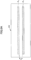
- the interconnect P S provided at a certain layer and the interconnect P D provided at a layer that is adjacent to the interconnect P S at an upper side or a lower side are provided not to overlap in a plan view.
- a distance L when the interconnect P S and the interconnect P D are seen in a plan view is at least greater than or equal to a width of an interconnect (greater than or equal to 0.05 mm, for example), and it is preferable that the distance L is as large as possible.
- the interconnect P S provided at the certain layer and the interconnect P D provided at the layer that is adjacent to the interconnect P S at the upper side or the lower side may be provided such that portions extending in substantially the same direction are not overlapped in a plan view.
- the interconnect P S and the interconnect P D may have portions that are partially overlapping with each other in a plan view.
- Fig. 5B illustrates such an example.
- the interconnect P S and the interconnect P D illustrated in Fig. 5B are provided such that portions extending substantially in the same direction (portions laterally extending in the drawing) are not overlapped with each other in a plan view.
- the interconnects include portions that are crossing in a plan view.
- a crossing angle is not an acute angle and the interconnects are crossing in a perpendicular direction as much as possible. This is to reduce generation of electromotive force by electromagnetic induction.
- the interconnect P S and the interconnect P D are provided in the same layer, it is preferable that the interconnect P S and the interconnect P D are not in parallel. Further, even when the interconnect P S and the interconnect P D are provided in different layers, it is preferable that the interconnect P S and the interconnect P D are not in parallel.
- the stacked interconnects of the package 410 are described with reference to Fig. 4 , Fig. 5A and Fig. 5B , it is preferable that the same counter measures are taken for the interconnects of the substrate 490. This is to furthermore reduce the cross-talk.
- H_SENS horizontal sensor signal
- V_SENS vertical sensor signal
- H_DRV horizontal driving signal
- V_DRV vertical drive signal
- interconnects are designed in consideration of Fig. 4 , Fig. 5A and Fig. 5B in the package 410, but interconnects are not designed in consideration of Fig. 4 , Fig. 5A and Fig. 5B in a conventional package (this is the same in the following).
- a GND is not provided between interconnects in each layer, or between layers in the vertical direction, and a portion at which interconnects in the vertical direction are overlapped or a portion at which the interconnects in the vertical direction are crossing in an acute angle are included, in the conventional package.
- the waveform of the V_SENS is the same as the waveform of the V_DRV in the conventional package.
- phases of the waveform of the V_SENS and the waveform of the V_DRV should be reversed 180 degrees, however, as the cross-talk from the V_DRV to the V_SENS is large, they became the same phase.
- the sensor interconnect and the drive interconnect are stacked, the sensor interconnect and the drive interconnect are placed not to overlap with each other in a plan view. Further, when the sensor interconnect and the drive interconnect are formed in a same layer, a GND interconnect is provided between the adjacent sensor interconnect and the drive interconnect. With this configuration, cross-talk generated between the sensor interconnect and the drive interconnect can be reduced, and a signal from the sensor interconnect can be accurately detected.
- the optical scanner module 400 when the sensor interconnect and the drive interconnect are stacked, it is preferable that a GND interconnect is provided between the sensor interconnect and the drive interconnect that are adjacent in the upper and lower direction. Further, when the sensor interconnect and the drive interconnect that are adjacent in the upper and lower direction are crossing with each other, it is preferable that they are placed such that to perpendicularly cross with each other. With this configuration, cross-talk generated between the sensor interconnect and the drive interconnect can be furthermore reduced, and a signal from the sensor interconnect can be furthermore accurately detected.
- Fig. 8 is a perspective view (No. 1) for describing strengthening the GND of the package.
- the package cover 420 is provided on the package 410 so as to cover the optical scanner apparatus 30 in the optical scanner module 400.
- the optical scanner apparatus 30 cannot be seen in Fig. 8 .
- An opening is provided at a substantially center portion of the package cover 420 that exposes a vicinity of the mirror 310 of the optical scanner apparatus 30, and the cover glass 430 that transmits incident light and output light is provided so as to cover the opening.
- GND interconnects P G are provided at an outer edge portion of a surface of the package 410 at which the optical scanner apparatus 30 is mounted and at a position that is exposed from the package cover 420 to be externally connected.
- Each of the GND interconnects P G is drawn from the GND interconnect in the package 410 to the surface of the package 410.
- the number of the GND interconnect P G may be one or plural.
- the GND interconnect P G is provided at each of four corners of the surface of the package 410 at which the optical scanner apparatus 30 is mounted.
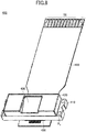
- Fig. 9A and Fig. 9B are perspective views (No. 2) for describing strengthening the GND of the package.
- the package 410 is fixed to a housing 600 while facing a GND interconnect P G side to the housing 600 by hold pins 700 (fixing member).
- the package cover 420 including the cover glass 430 is exposed at an opposite surface of the housing 600 from an opening provided in the housing 600, and light can be input into and output from the optical scanner apparatus 30.
- Fig. 9B illustrates a status in which the package 410 is attached to the housing 600 (not illustrated in Fig. 9B ).
- each of the hold pins 700 has a structure in which a cylindrical portion with a small diameter is substantially concentrically provided at a front end of a cylindrical portion with a large diameter.
- a side surface of the cylindrical portion with a large diameter of each of the hold pins 700 is contacted at a groove 410x having a substantially V shape provided at a side surface of the package 410, and the cylindrical portion with a small diameter is inserted in a hole provided in the housing 600 to fix the respective hold pin 700.
- a position of the package 410 with respect to the housing 600 can be adjusted (in other words, a position of the mirror 310 can be adjusted).
- the housing 600 is made of a metal or an insulating body whose surface is coated by a metal, and is grounded.
- the GND interconnect P G and the surface of the housing 600 are physically contacted, and both (both GNDs) are electrically connected.
- the housing 600 is a stable GND, the GND interconnect P G and the GND in the package 400 connected to the GND interconnect P G are strengthened.
- the cross-talk by the mutual capacitance can be furthermore suppressed.
- a vent 420x is provided in the package cover 420, and ultraviolet curing resin or the like is filled in the vent 420x to block the vent 420x.
- Fig. 10B illustrates the vent 420x in an enlarged manner before the vent 420x is filled with the ultraviolet curing resin or the like. The reason for providing the vent 420x is as follows.
- the structure of Fig. 10A may be manufactured by, for example, after bonding the cover glass 430 to the package cover 420, curing the package cover 420 including the cover glass 430 to the package 410 by a heat curing adhesive agent.
- gas in a sealed space sealed by the package cover 420 including the cover glass 430 and the package 410 may expand and the adhesive agent may be cured while the package cover 420 is floated.
- the adhesive agent is cured while the package cover 420 is floated, the sealed space cannot be sealed and dusts in air enter the sealed space.
- the dusts in air may collide against a surface of the mirror 310 and the mirror 310 may be contaminated. In order to prevent such contamination, it is necessary to seal with clean gas.
- the vent 420x is provided at the package cover 420.
- the expanded gas in the sealed space can be released from the vent 420x.
- the heat curing adhesive agent is cured, by blocking the vent 420x by ultraviolet curing resin or the like at ambient temperature again, the sealed space can be surely sealed without the package cover 420 being floated.
- the optical scanner control apparatus of the invention is applied to the laser scanning projector.
- the optical scanner control apparatus of the invention may be applied to various devices for displaying an image on a screen.
- an on-vehicle head up display, a head mount display, a laser printer, a laser scanning epilator, a laser head lamp, a laser radar or the like may be exemplified.
Landscapes
- Physics & Mathematics (AREA)
- General Physics & Mathematics (AREA)
- Optics & Photonics (AREA)
- Engineering & Computer Science (AREA)
- Computer Hardware Design (AREA)
- Microelectronics & Electronic Packaging (AREA)
- Mechanical Optical Scanning Systems (AREA)
- Mechanical Light Control Or Optical Switches (AREA)
- General Electrical Machinery Utilizing Piezoelectricity, Electrostriction Or Magnetostriction (AREA)
- Micromachines (AREA)
- Structure Of Printed Boards (AREA)
Abstract
Description
- The present invention relates to an optical scanner module and an optical scanner control apparatus.
- Conventionally, an optical scanner module is known in which an optical scanner apparatus that rotates a mirror around a rotation axis to reflect incident light such as laser light is mounted on a package. In this optical scanner module, a displacement sensor that detects an oscillation angle of the mirror under a status that the mirror is driven and oscillated is provided, inclination of the mirror is detected based on a signal output from the displacement sensor, and the mirror is controlled to be driven (see
Patent Document 1, for example). - [Patent Document 1] Japanese Laid-open Patent Publication No.
2014-235316 - However, a sensor interconnect connected to the displacement sensor and a drive interconnect through which a drive signal for oscillating the mirror passes may be drawn in the package in a complicated manner in the above described optical scanner module. Then, depending on a way of drawing the interconnects, cross-talk may be generated between the sensor interconnect and the drive interconnect, and there is a risk that a signal from the sensor interconnect cannot be accurately detected.
- The present invention is made in light of the above problems, and provides an optical scanner module capable of reducing cross-talk generated between a sensor interconnect and a drive interconnect.
- An optical scanner module (400), includes an optical scanner apparatus (30) that scans incident light by oscillating a mirror (310); and a package (410) on which the optical scanner apparatus (30) is mounted, wherein the optical scanner apparatus (30) includes a displacement sensor (391, 395, 396) that detects an oscillation angle of the mirror (310), wherein a sensor interconnect (PS) connected to the displacement sensor (391, 395, 396) and a drive interconnect (PD) through which a drive signal for oscillating the mirror (310) passes are respectively drawn from the optical scanner apparatus (30) into the package (410), wherein interconnect layers in which the sensor interconnect (PS) and the drive interconnect (PD) are formed are stacked, wherein the sensor interconnect (PS) and the drive interconnect (PD) are placed not to overlap in a plan view of the interconnect layers, and wherein a GND interconnect (PG) is provided between the sensor interconnect (PS) and the drive interconnect (PD) that are adjacent in a same interconnect layer.
- Here, the reference numerals in the brackets are provided for facilitating understanding and just an example, and the components are not limited to the illustrated embodiments.
- According to the disclosed technique, an optical scanner module capable of reducing cross-talk generated between a sensor interconnect and a drive interconnect can be provided.
-
-
Fig. 1 is a block diagram illustrating an example of an optical scanner control apparatus of a first embodiment; -
Fig. 2 is a plan view illustrating an example of an optical scanner apparatus constituting the optical scanner control apparatus; -
Fig. 3 is a perspective view for describing electric wiring of an optical scanner module; -
Fig. 4 is a view (No. 1) for describing a method of suppressing cross-talk; -
Fig. 5A is a view (No. 2) for describing a method of suppressing cross-talk; -
Fig. 5B is a view (No. 3) for describing a method of suppressing cross-talk; -
Fig. 6 is a view (No. 1) for describing an actual measurement of cross-talk; -
Fig. 7A is a view (No. 2) for describing an actual measurement of cross-talk; -
Fig. 7B is a view (No. 3) for describing an actual measurement of cross-talk; -
Fig. 8 is a perspective view (No. 1) for describing GND strengthening of a package; -
Fig. 9A is a perspective view (No. 2) for describing GND strengthening of a package; -
Fig. 9B is a perspective view (No. 3) for describing GND strengthening of a package; -
Fig. 10A is a view for describing a vent provided at a package cover; and -
Fig. 10B is a view for describing the vent provided at the package cover. - Embodiments of the invention will be described herein with reference to drawings. It is to be noted that, in each of the drawings, the same components are given the same reference numerals, and explanations may not be repeated.
-
Fig. 1 is a block diagram illustrating an example of an optical scanner control apparatus of a first embodiment.Fig. 2 is a plan view illustrating an example of an optical scanner apparatus that constitutes the optical scanner control apparatus. - First, with reference to
Fig. 1 andFig. 2 , a schematic structure of an opticalscanner control apparatus 1 is described. The opticalscanner control apparatus 1 includes, as main constituents, acircuit unit 10, alight source unit 20, anoptical scanner apparatus 30, anoptical unit 40, ascreen 50 and a lightquantity detection sensor 60. The opticalscanner control apparatus 1 is, for example, a laser scanning projector. - The
circuit unit 10 is a portion that controls thelight source unit 20 and theoptical scanner apparatus 30, and may be constituted by, for example, asystem controller 11, a CPU (Central Processing Unit) 12, various driving circuits such as abuffer circuit 13, amirror driving circuit 14, alaser driving circuit 15 and atemperature control circuit 16, and the like. - The
light source unit 20 includes anLD module 21, atemperature control unit 22, atemperature sensor 23 and abeam attenuating filter 24. - The
LD module 21 includeslasers quantity detection sensor 215 that monitors the latest light quantity of each of thelasers laser 211R may be a red semiconductor laser and may output light with wavelength λR (640 nm, for example), for example. Thelaser 211G may be a green semiconductor laser and may output light with wavelength λG (530 nm, for example), for example. Thelaser 211B may be a blue semiconductor laser and may output light with wavelength λB (445 nm, for example), for example. As the lightquantity detection sensor 215, for example, a photodiode or the like may be used. The lightquantity detection sensor 215 may be placed at an appropriate position at which the light quantity before passing thebeam attenuating filter 24 can be detected. - The
temperature control unit 22 may control thelasers temperature sensor 23 may detect temperature of each of thelasers temperature control unit 22, for example, a Peltier element may be used. As thetemperature sensor 23, for example, a thermistor may be used. - The
beam attenuating filter 24 is placed at a preceding stage of amirror 310, and light (synthesized light) output from thelasers beam attenuating filter 24 has a function to adjust brightness on thescreen 50. As thebeam attenuating filter 24, an ND (Neutral Density) filter, a liquid crystal device (liquid crystal element), a polarizing filter or the like may be used. Thebeam attenuating filter 24 is, for example, inserted to be inclined with respect to an optical axis of incident light, and light that does not pass (attenuated light) is absorbed or reflected by thebeam attenuating filter 24. - The
optical scanner apparatus 30 is, for example, a MEMS (Micro Electro Mechanical System) that drives themirror 310 by a piezo-electric element. Themirror 310 functions as scanning means that forms an image on thescreen 50 by reflecting light (synthesized light) output from thelasers - Specifically, as illustrated in
Fig. 2 , theoptical scanner apparatus 30 includes themirror 310, amirror support portion 320,torsion beams beams beams movable frame 360, drivingbeams frame 380. The driving beams 350A and 350B respectively include drivingsources sources beams mirror 310 in upper-lower or left-right directions. - The
mirror support portion 320 is provided withslits 322 along a circumference of themirror 310. By providing theslits 322, themirror support portion 320 can be lightened and stress that is generated when transmitting torsion by thetorsion beams mirror 310 can be reduced. - In the
optical scanner apparatus 30, themirror 310 is supported at a front surface of themirror support portion 320, and themirror support portion 320 is connected to end portions of thetorsion beams mirror support portion 320. Thetorsion beams mirror support portion 320 from both sides in an axial direction by extending in the axial direction. When thetorsion beams mirror 310 supported by themirror support portion 320 is oscillated so that reflected light irradiated on themirror 310 is scanned. Thetorsion beams beams beams - The driving beams 350A and 350B, the connecting
beams torsion beams mirror support portion 320 and themirror 310 are surrounded by themovable frame 360. One side of each of the drivingbeams movable frame 360. The other side of thedriving beam 350A extends an inner side to be connected to the connectingbeams driving beam 350B similarly extends an inner side to be connected to the connectingbeams - The driving beams 350A and 350B are provided as a pair in a direction perpendicular to the
torsion beams mirror 310 and themirror support portion 320 therebetween. The drivingsources beams sources beams driving sources - Thus, by alternately applying drive voltages of different phases to the
driving beam 350A and thedriving beam 350B, respectively, thedriving beam 350A and thedriving beam 350B alternately oscillate opposite directions (upper or lower) at left-right sides of themirror 310. With this, themirror 310 can be oscillated around an axis while having thetorsion beams mirror 310 is oscillated around the axis of thetorsion beams beams mirror 310 to be oscillated at a high speed. - As such, the driving
beams horizontal driving sources mirror 310 in the horizontal direction, respectively. - One end of each of the driving
beams movable frame 360. The driving beams 370A and 370B are connected to themovable frame 360 at positions that are point symmetry with respect to themirror 310 as a center, and are provided as a pair to interpose themovable frame 360 therebetween from left-right sides, respectively. Thedriving beam 370A includes multiple beams each extending in parallel with respect to thedriving beam 350A where adjacent beams are connected with each other at respective end portions to form a zig-zag shape as a whole. The other end of thedriving beam 370A is connected to an inner side of the fixedframe 380. Thedriving beam 370B includes, similarly, multiple beams each extending in parallel with respect to thedriving beam 350B where adjacent beams are connected with each other at respective end portions to form a zig-zag shape as a whole. The other end of thedriving beam 370B is connected to an inner side of the fixedframe 380. - The driving
sources beams sources beams - In the driving
beams adjacent driving sources movable frame 360. The driving beams 370A and 370B oscillate themirror 310 in the vertical direction, which is perpendicular to the horizontal direction by this operation. For example, for the vertical driving by the drivingbeams - For example, the driving
source 371R includes driving sources 371AR, 371BR, 371CR, 371DR, 371ER and 371FR that are aligned rightward from amovable frame 360 side. The drivingsource 371L includes driving sources 371AL, 371BL, 371CL, 371DL, 371EL and 371FL that are aligned leftward from amovable frame 360 side. In such a case, by driving the driving sources 371AR, 371BL, 371CR, 371DL, 371ER and 371FL by the same waveform, and the driving sources 371BR, 371AL, 371DR, 371CL, 371FR and 371EL by the waveform with different phase from that for the driving sources 371AR, 371BL, 371CR, 371DL, 371ER and 371FL, themirror 310 can be oscillated in the vertical direction. - As such, the driving
beams sources mirror 310 in the vertical direction, respectively. - Drive interconnects that apply drive voltage to the upper electrode and the lower electrode of the driving
source 351A are connected to predetermined terminals of a group of terminals TA provided at the fixedframe 380. Drive interconnects that apply drive voltage to the upper electrode and the lower electrode of the drivingsource 351B are connected to predetermined terminals of a group of terminals TB provided at the fixedframe 380. Drive interconnects that apply drive voltage to the upper electrode and the lower electrode of the drivingsource 371R are connected to predetermined terminals of the group of terminals TA provided at the fixedframe 380. Drive interconnects that apply drive voltage to the upper electrode and the lower electrode of the drivingsource 371L are connected to predetermined terminals of the group of terminals TB provided at the fixedframe 380. - The
optical scanner apparatus 30 includes ahorizontal displacement sensor 391 that detects inclination (oscillation angle in the horizontal direction) of themirror 310 in the horizontal direction when the drive voltage is applied to thedriving sources mirror 310 is oscillated in the horizontal direction. Numerals "392", "393" and "394" are dummy sensors. - The
optical scanner apparatus 30 includesvertical displacement sensors mirror 310 in the vertical direction when the voltage is applied to the drivingsources mirror 310 is oscillated in the vertical direction. - Referring back to
Fig. 1 , theoptical unit 40 is an optical system that projects light scanned by theoptical scanner apparatus 30 on thescreen 50. The light input in theoptical unit 40 from theoptical scanner apparatus 30 forms an image on thescreen 50, and an image corresponding to the image signal is displayed on thescreen 50. - The
screen 50 includes, for example, a micro-lens array for removing noises of an image that are seen as particles called speckles. In such a case, each of the micro-lenses that compose the micro-lens array corresponds to a pixel of a display, and it is preferable that an irradiated laser beam is equal to a size of the micro-lens or less than the size of the micro-lens. - The light
quantity detection sensor 60 may be placed at an appropriate position at which the quantity of the light that passes thebeam attenuating filter 24 can be detected. The lightquantity detection sensor 60 is capable of independently detecting the light quantity of each of thelasers beam attenuating filter 24. As the lightquantity detection sensor 60, for example, one or a plurality of photodiodes or the like may be used. - Next, an operation of the optical
scanner control apparatus 1 is schematically described. Thesystem controller 11, that is a control unit, generates a drive signal based on a signal obtained via the sensor interconnect, for example. Themirror driving circuit 14 drives themirror 310 based on the drive signal generated by thesystem controller 11, for example. - More specifically, the
system controller 11 may control an oscillating angle of themirror 310, for example. Thesystem controller 11 may monitor inclination of themirror 310 in the horizontal direction and the vertical direction obtained at thehorizontal displacement sensor 391 and thevertical displacement sensors buffer circuit 13, and supply an angle control signal to amirror driving circuit 14, for example. Then, themirror driving circuit 14 may supply predetermined drive signals to the driving beams 351 and 352 and the driving beams 371 and 372 based on the angle control signal from thesystem controller 11 to drive (scan) themirror 310 at a predetermined angle. - Further, the
system controller 11 may supply, for example, a digital image signal to alaser driving circuit 15. Then, thelaser driving circuit 15 may supplies predetermined current to thelasers system controller 11. With this, thelasers - The
CPU 12 may monitor primitive light quantity output from each of thelasers quantity detection sensor 215, and supply a light quantity control signal to theLD module 21, for example. Each of thelasers CPU 12. - Here, the light
quantity detection sensor 215 may include three sensors each independently detecting the light quantity of the each of the lights output from thelasers quantity detection sensor 215 may be constituted by a single sensor. In such a case, it is possible to control the light quantity of the light out from each of thelasers lasers - Further, the
CPU 12 may monitor temperatures of thelasers temperature sensor 23, and supply a temperature control signal to atemperature control circuit 16. Then, thetemperature control circuit 16 supplies predetermined current to thetemperature control unit 22 based on the temperature control signal from theCPU 12. With this, thetemperature control unit 22 is heated or cooled, and each of the lasers is controlled to be predetermined temperature. - The light
quantity detection sensor 60 detects light quantity of light after passing through thebeam attenuating filter 24. As described above, the lightquantity detection sensor 215 for adjusting the light quantity of each of the lasers is mounted in theLD module 21, and the lightquantity detection sensor 215 detects primitive output light quantity of each of thelasers scanner control apparatus 1 is formed by light imaged on thescreen 50, there may be a case that the light is not appropriately adjusted by an adjustment based on the primitive laser light quantity. - For example, as the
beam attenuating filter 24 is provided on an optical path, depending on characteristics of thebeam attenuating filter 24, there may be a case that an expected attenuating ratio cannot be obtained, and the light quantity after passing thebeam attenuating filter 24 does not become an expected value. Further, when attenuating ratios of R / G / B of thebeam attenuating filter 24 are dispersed, balance after passing through thebeam attenuating filter 24 may not be retained. Further, there may be a case that characteristics of theoptical scanner apparatus 30 are changed due to temperature or aged deterioration. Such problems cannot be dissolved even if the light quantity before passing through theoptical scanner apparatus 30 is precisely controlled by the lightquantity detection sensor 215. - Thus, in the optical
scanner control apparatus 1, as light quantity detection means for detecting the light quantity after passing through thebeam attenuating filter 24, a lightquantity detection sensor 60, is provided. A detection result of the lightquantity detection sensor 60 is input in theCPU 12, and theCPU 12 may supply a light quantity control signal for controlling a current value of each of the lasers to theLD module 21 based on the light quantity detected by the lightquantity detection sensor 60. - With this, light quantity of the laser light including variation of the characteristics of the
beam attenuating filter 24 can be detected. Thus, the light quantity can be accurately controlled so as to correspond to an image that is actually displayed on thescreen 50. Here, the lightquantity detection sensor 60 may independently detect the light quantity of each of thelasers CPU 12 may control the current value of each of the lasers based on the respective light quantity detected by the lightquantity detection sensor 60. -
Fig. 3 is a perspective view for describing electric wiring of the optical scanner module. As illustrated inFig. 3 , theoptical scanner module 400 includes theoptical scanner apparatus 30, apackage 410, aconnector 450 and asubstrate 490. As will be described later, theoptical scanner module 400 may include apackage cover 420, acover glass 430 and the like (seeFig. 8 and the like). - In the
optical scanner module 400, theoptical scanner apparatus 30 is mounted on thepackage 410, and thepackage 410 is connected to thesubstrate 490 via theconnector 450. Thepackage 410 is, for example, a ceramic package, and stacked interconnects (10 layers of interconnects, for example) are provided in thepackage 410. Here, thepackage 410 may be a printed wiring board and the like, other than the ceramic, and a base material is not limited as long as it is possible to form a multilayer interconnection board (substrate). - The
substrate 490 is, for example, a flexible printed wiring board. A sensor interconnect PS, a drive interconnect PD and a GND interconnect PG, which will be described later, are drawn from theoptical scanner apparatus 30 into thepackage 410, and further drawn in thesubstrate 490. - As described above, when controlling an oscillating angle of the
mirror 310, thesystem controller 11 uses sensor signals obtained by thehorizontal displacement sensor 391 and thevertical displacement sensors horizontal displacement sensor 391 and thevertical displacement sensors - Sensor signals of the
horizontal displacement sensor 391 and thevertical displacement sensors optical scanner apparatus 30 to a group of terminals TC and TD of thepackage 410. Then, the sensor signals pass through the stacked interconnects in thepackage 410, and further pass through theconnector 450 and interconnects of thesubstrate 490 to reach a group of terminals TE. Further, similarly as the sensor signals, a horizontal driving signal and a vertical drive signal for driving themirror 310 are connected from the group of terminals TA and TB of theoptical scanner apparatus 30 to the group of terminals TE. - If an electrical cross-talk between interconnects occurs in the interconnects from the
optical scanner apparatus 30 to the group of terminals TE, the sensor signals cannot be accurately detected. In particular, if cross-talk occurs between the horizontal driving signal and thehorizontal displacement sensor 391, and between the vertical drive signal and thevertical displacement sensors - Thus, even if the
mirror 310 fails, and does not oscillate, as long as the interconnect is electrically connected, there is a rick that a defect will be generated, such as a sensor output is detected. In particular, as a plurality of interconnects are three-dimensionally provided in thepackage 410 including the stacked interconnects, and an electrical cross-talk is easily generated, a countermeasure to prevent generation of an electrical cross-talk is necessary. - The above described electrical cross-talk strongly depends on mutual capacitance and mutual inductance between interconnects.
- A cross-talk by mutual capacitance is a phenomenon in which adjacent interconnects become a capacitor when having capacitance, and if one of the interconnects is electrically charged, electrical charge is induced even through lines are directly connected, and the other of the interconnects is also electrically charged. In such a case, the magnitude of the cross-talk is determined by the mutual capacitance and input voltage applied to the interconnects. Thus, according to the embodiment, in order to suppress (reduce) the cross-talk by the mutual capacitance, the following countermeasure is taken for the stacked interconnects of the
package 410. - Specifically, as illustrated in
Fig. 4 , in each layer of the stacked interconnects, a GND interconnect PG is provided to be sandwiched between an interconnect PS and an interconnect PD. Further, a GND surface (GND layer) are provided around the interconnect PS and the interconnect PD. With this, capacitance is hardly formed between the interconnect PS and the interconnect PD. Here, inFig. 4 , the interconnect PS is a sensor interconnect that is connected to the displacement sensor, and the interconnect PD is a drive interconnect through which a drive signal for oscillating themirror 310 passes (the same in the following). - Further, in each layer of the stacked interconnects, it is preferable that a GND layer LG including a GND surface whose entire surface is grounded is sandwiched between interconnect layers L1 and L2 in each of which the interconnect PS and the interconnect PD are formed. This means that it is preferable that a GND is sandwiched between interconnects in the vertical direction not only in a planar direction of the interconnects. With this, each of the interconnect PS and the interconnect PD is surrounded by the GND interconnect PG provided between the interconnects and the GND surface provided at the lower GND layer LG, and capacitance is hardly generated. Although the it is exemplified that the entire surface of the GND layer LG is formed as a GND layer, the GND interconnect PG may be provided right below each of the interconnects of the interconnect layers L1 and L2 along each of the interconnects PS and PD. This means that the GND interconnect PG may be linearly provided, not as a plane.
- A cross-talk by mutual inductance is a phenomenon in which a magnetic field is generated by electromagnetic induction when a current flowing through each of the interconnects varies in accordance with time, and an electromotive force is generated by the magnetic field. In such a case, the magnitude of the cross-talk is determined by variability of current with time and an amount of the current. Thus, according to the embodiment, in order to suppress (reduce) the cross-talk by the mutual inductance, the following countermeasure is taken for the stacked interconnects of the
package 410. - Specifically, as illustrated in a plan view of
Fig. 5A , in each layer of the stacked interconnects, the interconnect PS provided at a certain layer and the interconnect PD provided at a layer that is adjacent to the interconnect PS at an upper side or a lower side are provided not to overlap in a plan view. A distance L when the interconnect PS and the interconnect PD are seen in a plan view, is at least greater than or equal to a width of an interconnect (greater than or equal to 0.05 mm, for example), and it is preferable that the distance L is as large as possible. - Here, the interconnect PS provided at the certain layer and the interconnect PD provided at the layer that is adjacent to the interconnect PS at the upper side or the lower side may be provided such that portions extending in substantially the same direction are not overlapped in a plan view. However, the interconnect PS and the interconnect PD may have portions that are partially overlapping with each other in a plan view.
Fig. 5B illustrates such an example. The interconnect PS and the interconnect PD illustrated inFig. 5B are provided such that portions extending substantially in the same direction (portions laterally extending in the drawing) are not overlapped with each other in a plan view. However, the interconnects include portions that are crossing in a plan view. - As such, as illustrated by a plan view of
Fig. 5B , when the interconnects (the interconnect PS and the interconnect PD) are crossing with each other, it is preferable that a crossing angle is not an acute angle and the interconnects are crossing in a perpendicular direction as much as possible. This is to reduce generation of electromotive force by electromagnetic induction. Further, when the interconnect PS and the interconnect PD are provided in the same layer, it is preferable that the interconnect PS and the interconnect PD are not in parallel. Further, even when the interconnect PS and the interconnect PD are provided in different layers, it is preferable that the interconnect PS and the interconnect PD are not in parallel. - Although the stacked interconnects of the
package 410 are described with reference toFig. 4 ,Fig. 5A andFig. 5B , it is preferable that the same counter measures are taken for the interconnects of thesubstrate 490. This is to furthermore reduce the cross-talk. - Next, suppression of the cross-talk described above with reference to
Fig. 3 to Fig. 5B was studied. Here, the horizontal sensor signal is referred to as "H_SENS", the vertical sensor signal is referred to as "V_SENS" the horizontal driving signal is referred to as "H_DRV" and the vertical drive signal is referred to as "V_DRV". - Specifically, simulations of the mutual capacitance and the mutual inductance between H_DRV and H_SENS, between H_DRV and V_SENS, between V_DRV and H_SENS, and between V_DRV and V_SENS were conducted. Results are illustrated in Table 1 and Table 2.
- Here, interconnects are designed in consideration of
Fig. 4 ,Fig. 5A andFig. 5B in thepackage 410, but interconnects are not designed in consideration ofFig. 4 ,Fig. 5A andFig. 5B in a conventional package (this is the same in the following). This means that a GND is not provided between interconnects in each layer, or between layers in the vertical direction, and a portion at which interconnects in the vertical direction are overlapped or a portion at which the interconnects in the vertical direction are crossing in an acute angle are included, in the conventional package.[Table 1] MUTUAL CAPACITANCE SIMULATION VALUE CONVENTIONAL PACKAGE PACKAGE 400 UNIT [pF] H_DRV V_DRV H_DRV V_DRV H_SENS 1.31 7.72 0.07 0.02 V_SENS 0.47 9.17 0.01 0.13 [Table 2] MUTUAL INDUCTANCE SIMULATION VALUE CONVENTIONAL PACKAGE PACKAGE 400 UNIT [nH] H_DRV V_DRV H_DRV V_DRV H_SENS 0.80 0.90 0.78 0.74 V_SENS 0.85 1.07 0.71 0.87 - As illustrated in Table 1 and Table 2, it can be understood that the mutual capacitance and the mutual inductance are reduced in the
package 410 compared with the conventional package. In particular, the mutual capacitance is largely reduced. - Next, under a status that the
optical scanner apparatus 30 was not mounted on thepackage 410 as illustrated inFig. 6 , cross-talk to the H_SENS when applying predetermined voltage on the H_DRV, and cross-talk to the V_SENS when applying predetermined voltage on the V_DRV were actually measured. Results are illustrated in Table 3.[Table 3] VOLTAGE APPLIED TERMINAL CROSS-TALK MEASUREMENT TERMINAL CONVENTIONAL PACKAGE PACKAGE 400 IMPROVED EFFECT H_DRV H_SENS 80 mV 20 mV -75% V_DRV V_SENS 1,200 mV 200 mV -84% - As illustrated in Table 3, it was confirmed that the cross-talk was improved for 75% at the horizontal side and 84% at the vertical in the
package 410 compared with the conventional package. - Next, under a status that the
optical scanner apparatus 30 was mounted on thepackage 410 as illustrated inFig. 3 , cross-talk to the H_SENS when applying predetermined voltage on the H_DRV, and cross-talk to the V_SENS when applying predetermined voltage on the V_DRV were actually measured. Results are illustrated inFig. 7A andFig. 7B .Fig. 7A illustrates the results of the conventional package, andFig. 7B illustrates the results of thepackage 410. - As illustrated in
Fig. 7A , the waveform of the V_SENS is the same as the waveform of the V_DRV in the conventional package. According to the structure of theoptical scanner apparatus 30, originally, phases of the waveform of the V_SENS and the waveform of the V_DRV should be reversed 180 degrees, however, as the cross-talk from the V_DRV to the V_SENS is large, they became the same phase. - On the other hand, as illustrated in
Fig. 7B , it can be understood that phases of the waveform of the V_SENS and the waveform of theV_DRV package 410 were reversed 180 degrees in accordance with a theory, and an original sensor waveform that reflected a driving status of themirror 310 was output to the caV_SENS. - As such, in the
optical scanner module 400, when the sensor interconnect and the drive interconnect are stacked, the sensor interconnect and the drive interconnect are placed not to overlap with each other in a plan view. Further, when the sensor interconnect and the drive interconnect are formed in a same layer, a GND interconnect is provided between the adjacent sensor interconnect and the drive interconnect. With this configuration, cross-talk generated between the sensor interconnect and the drive interconnect can be reduced, and a signal from the sensor interconnect can be accurately detected. - Further, in the
optical scanner module 400, when the sensor interconnect and the drive interconnect are stacked, it is preferable that a GND interconnect is provided between the sensor interconnect and the drive interconnect that are adjacent in the upper and lower direction. Further, when the sensor interconnect and the drive interconnect that are adjacent in the upper and lower direction are crossing with each other, it is preferable that they are placed such that to perpendicularly cross with each other. With this configuration, cross-talk generated between the sensor interconnect and the drive interconnect can be furthermore reduced, and a signal from the sensor interconnect can be furthermore accurately detected. - In a second embodiment, an example in which the GND is strengthened is described. Here, the same components that are already described in the above embodiment may not be repeated.
-
Fig. 8 is a perspective view (No. 1) for describing strengthening the GND of the package. As illustrated inFig. 8 , thepackage cover 420 is provided on thepackage 410 so as to cover theoptical scanner apparatus 30 in theoptical scanner module 400. Here, as theoptical scanner apparatus 30 is covered by thepackage cover 420, theoptical scanner apparatus 30 cannot be seen inFig. 8 . - An opening is provided at a substantially center portion of the
package cover 420 that exposes a vicinity of themirror 310 of theoptical scanner apparatus 30, and thecover glass 430 that transmits incident light and output light is provided so as to cover the opening. - Further, GND interconnects PG are provided at an outer edge portion of a surface of the
package 410 at which theoptical scanner apparatus 30 is mounted and at a position that is exposed from thepackage cover 420 to be externally connected. Each of the GND interconnects PG is drawn from the GND interconnect in thepackage 410 to the surface of thepackage 410. The number of the GND interconnect PG may be one or plural. As an example, the GND interconnect PG is provided at each of four corners of the surface of thepackage 410 at which theoptical scanner apparatus 30 is mounted. -
Fig. 9A andFig. 9B are perspective views (No. 2) for describing strengthening the GND of the package. As illustrated inFig. 9A , thepackage 410 is fixed to ahousing 600 while facing a GND interconnect PG side to thehousing 600 by hold pins 700 (fixing member). Thepackage cover 420 including thecover glass 430 is exposed at an opposite surface of thehousing 600 from an opening provided in thehousing 600, and light can be input into and output from theoptical scanner apparatus 30. -
Fig. 9B illustrates a status in which thepackage 410 is attached to the housing 600 (not illustrated inFig. 9B ). As illustrated inFig. 9B , each of the hold pins 700 has a structure in which a cylindrical portion with a small diameter is substantially concentrically provided at a front end of a cylindrical portion with a large diameter. - While pressing and contacting the
package 410 to thehousing 600, a side surface of the cylindrical portion with a large diameter of each of the hold pins 700 is contacted at agroove 410x having a substantially V shape provided at a side surface of thepackage 410, and the cylindrical portion with a small diameter is inserted in a hole provided in thehousing 600 to fix therespective hold pin 700. At this time, by forming the hole to be larger, and laterally moving thehold pin 700, a position of thepackage 410 with respect to thehousing 600 can be adjusted (in other words, a position of themirror 310 can be adjusted). - The
housing 600 is made of a metal or an insulating body whose surface is coated by a metal, and is grounded. When attaching thepackage 410 to thehousing 600, the GND interconnect PG and the surface of thehousing 600 are physically contacted, and both (both GNDs) are electrically connected. As thehousing 600 is a stable GND, the GND interconnect PG and the GND in thepackage 400 connected to the GND interconnect PG are strengthened. Thus, by strengthening the GND as described in the second embodiment, in addition to the method of suppressing the cross-talk by the mutual capacitance described in the first embodiment, the cross-talk by the mutual capacitance can be furthermore suppressed. - As illustrated in
Fig. 10A , avent 420x is provided in thepackage cover 420, and ultraviolet curing resin or the like is filled in thevent 420x to block thevent 420x.Fig. 10B illustrates thevent 420x in an enlarged manner before thevent 420x is filled with the ultraviolet curing resin or the like. The reason for providing thevent 420x is as follows. - The structure of
Fig. 10A may be manufactured by, for example, after bonding thecover glass 430 to thepackage cover 420, curing thepackage cover 420 including thecover glass 430 to thepackage 410 by a heat curing adhesive agent. - However, when curing the heat curing adhesive agent, gas in a sealed space sealed by the
package cover 420 including thecover glass 430 and thepackage 410 may expand and the adhesive agent may be cured while thepackage cover 420 is floated. - If the adhesive agent is cured while the
package cover 420 is floated, the sealed space cannot be sealed and dusts in air enter the sealed space. At this time, as themirror 310 is driven at high-speed, the dusts in air may collide against a surface of themirror 310 and themirror 310 may be contaminated. In order to prevent such contamination, it is necessary to seal with clean gas. - Thus, the
vent 420x is provided at thepackage cover 420. With this configuration, when curing the heat curing adhesive agent, the expanded gas in the sealed space can be released from thevent 420x. Then, after the heat curing adhesive agent is cured, by blocking thevent 420x by ultraviolet curing resin or the like at ambient temperature again, the sealed space can be surely sealed without thepackage cover 420 being floated. - Although preferred embodiments have been specifically illustrated and described, it is to be understood that minor modifications may be made therein without departing from the spirit and scope of the invention as defined by the claims.
- For example, an example is described in the above embodiments in which the optical scanner control apparatus of the invention is applied to the laser scanning projector. However, this is just an example, and the optical scanner control apparatus of the invention may be applied to various devices for displaying an image on a screen. For such devices, for example, an on-vehicle head up display, a head mount display, a laser printer, a laser scanning epilator, a laser head lamp, a laser radar or the like may be exemplified.
- The present application is based on and claims the benefit of priority of Japanese Priority Application No.
2015-196872 filed on October 2, 2015 - 1
- optical scanner control apparatus
- 10
- circuit unit
- 11
- system controller
- 12
- CPU
- 13
- buffer circuit
- 14
- mirror driving circuit
- 15
- laser driving circuit
- 16
- temperature control circuit
- 20
- light source unit
- 21
- LD module
- 22
- temperature control unit
- 23
- temperature sensor
- 24
- beam attenuating filter
- 30
- optical scanner apparatus
- 40
- optical unit
- 50
- screen
- 60
- light quantity detection sensor
- 211R, 211G, 211B
- laser
- 215
- light quantity detection sensor
- 310
- mirror
- 320
- mirror support portion
- 322
- slit
- 330A, 330B
- torsion beam
- 340A, 340B
- connecting beam
- 350A, 350B, 370A, 370B
- driving beam
- 351A, 351B, 371R, 371L
- driving source
- 360
- movable frame
- 380
- fixed frame
- 391
- horizontal displacement sensor
- 392, 393, 394
- dummy sensor
- 395, 396
- vertical displacement sensor
- 400
- optical scanner module
- 410
- package
- 410x
- groove
- 420
- package cover
- 420x
- vent
- 430
- cover glass
- 450
- connector
- 490
- substrate
- 600
- housing
- 700
- hold pin
Claims (6)
- An optical scanner module, comprising:an optical scanner apparatus that scans incident light by oscillating a mirror; anda package on which the optical scanner apparatus is mounted,wherein the optical scanner apparatus includes a displacement sensor that detects an oscillation angle of the mirror,wherein a sensor interconnect connected to the displacement sensor and a drive interconnect through which a drive signal for oscillating the mirror passes are respectively drawn from the optical scanner apparatus into the package,wherein interconnect layers in which the sensor interconnect and the drive interconnect are formed are stacked,wherein the sensor interconnect and the drive interconnect are placed not to overlap in a plan view of the interconnect layers, andwherein a GND interconnect is provided between the sensor interconnect and the drive interconnect that are adjacent in a same interconnect layer.
- The optical scanner module according to claim 1, wherein a GND layer is provided at upper or lower of each of the interconnect layers.
- The optical scanner module according to claim 1, wherein a GND interconnect is provided at upper or lower of each of the interconnect layers to extend along each of the sensor interconnect and the drive interconnect.
- The optical scanner module according to claim 1, wherein when the sensor interconnect and the drive interconnect that are adjacent in an upper and lower direction are crossing with each other, the sensor interconnect and the drive interconnect are provided to perpendicular to each other.
- The optical scanner module according to claim 1, wherein the GND interconnect is drawn from inside of the package to a surface of the package to be exposed at the surface, and is configured to be externally connectable.
- An optical scanner control apparatus comprising:the optical scanner module of claim 1;a control unit that generates the drive signal based on a signal obtained via the sensor interconnect; anda driving circuit that drives the mirror based on the drive signal generated by the control unit.
Applications Claiming Priority (2)
| Application Number | Priority Date | Filing Date | Title |
|---|---|---|---|
| JP2015196872A JP6741933B2 (en) | 2015-10-02 | 2015-10-02 | Optical scanning module, optical scanning control device |
| PCT/IB2016/001637 WO2017055931A1 (en) | 2015-10-02 | 2016-11-18 | Optical scanning module and optical scanning control device |
Publications (3)
| Publication Number | Publication Date |
|---|---|
| EP3346312A1 true EP3346312A1 (en) | 2018-07-11 |
| EP3346312A4 EP3346312A4 (en) | 2019-03-06 |
| EP3346312B1 EP3346312B1 (en) | 2022-07-13 |
Family
ID=58422766
Family Applications (1)
| Application Number | Title | Priority Date | Filing Date |
|---|---|---|---|
| EP16850458.7A Active EP3346312B1 (en) | 2015-10-02 | 2016-11-18 | Optical scanning module and optical scanning control device |
Country Status (5)
| Country | Link |
|---|---|
| US (2) | US10654708B2 (en) |
| EP (1) | EP3346312B1 (en) |
| JP (1) | JP6741933B2 (en) |
| CN (1) | CN108337904B (en) |
| WO (1) | WO2017055931A1 (en) |
Cited By (1)
| Publication number | Priority date | Publication date | Assignee | Title |
|---|---|---|---|---|
| CN112600360A (en) * | 2020-12-14 | 2021-04-02 | 基合半导体(宁波)有限公司 | Focusing motor, closed-loop control method of focusing motor and camera equipment |
Families Citing this family (11)
| Publication number | Priority date | Publication date | Assignee | Title |
|---|---|---|---|---|
| JP6662392B2 (en) * | 2015-12-22 | 2020-03-11 | 株式会社リコー | Rotating device, optical scanning device, and image display device |
| JP7140959B2 (en) | 2018-03-14 | 2022-09-22 | ミツミ電機株式会社 | Actuator and optical scanner |
| JP7024612B2 (en) * | 2018-05-31 | 2022-02-24 | 株式会社リコー | Light deflection device and its manufacturing method, image projection device, object recognition device, laser head lamp device, optical writing device, and moving object |
| JP7167500B2 (en) * | 2018-06-25 | 2022-11-09 | 株式会社リコー | Mobile devices, image projection devices, head-up displays, laser headlamps, head-mounted displays, object recognition devices, and vehicles |
| JP7157332B2 (en) | 2018-12-28 | 2022-10-20 | ミツミ電機株式会社 | Optical scanning device and its control method |
| US11307403B2 (en) * | 2019-04-05 | 2022-04-19 | Infineon Technologies Ag | Synchronization of microelectromechanical system (MEMS) mirrors |
| US11175491B2 (en) * | 2019-04-25 | 2021-11-16 | Microsoft Technology Licensing, Llc | Non-resonant microelectromechanical systems scanner with piezoelectric actuators |
| JP7315827B2 (en) * | 2019-07-01 | 2023-07-27 | ミツミ電機株式会社 | Optical scanning device and its control method |
| US11728611B2 (en) * | 2019-09-04 | 2023-08-15 | Lumentum Operations Llc | Isothermal enclosure with optical aperture |
| DE102021202120A1 (en) * | 2021-03-04 | 2022-09-08 | MICRO-EPSILON-MESSTECHNIK GmbH & Co. K.G. | Actuator Sensor System and Fast Steering Mirror (FSM) |
| JP7686596B2 (en) * | 2022-03-30 | 2025-06-02 | ビアメカニクス株式会社 | Laser Processing Equipment |
Family Cites Families (25)
| Publication number | Priority date | Publication date | Assignee | Title |
|---|---|---|---|---|
| JPS59214241A (en) | 1983-05-20 | 1984-12-04 | Mitsubishi Electric Corp | Semiconductor device |
| JP2759573B2 (en) * | 1992-01-23 | 1998-05-28 | 株式会社日立製作所 | Circuit board wiring pattern determination method |
| JP4058234B2 (en) * | 1999-12-22 | 2008-03-05 | 株式会社東芝 | Semiconductor device |
| US6483176B2 (en) | 1999-12-22 | 2002-11-19 | Kabushiki Kaisha Toshiba | Semiconductor with multilayer wiring structure that offer high speed performance |
| US6731513B2 (en) | 2002-03-15 | 2004-05-04 | Memx, Inc. | Shielded multi-conductor interconnect bus for MEMS |
| JP2004235542A (en) * | 2003-01-31 | 2004-08-19 | Sharp Corp | Electric circuit device provided with bus wiring for reducing crosstalk noise, wiring method of bus wiring of electric circuit device, wiring system of bus wiring of electric circuit device |
| KR100576846B1 (en) * | 2003-04-07 | 2006-05-10 | 삼성전기주식회사 | MEMS Variable Optical Attenuator |
| JP2005039152A (en) | 2003-07-18 | 2005-02-10 | Shinko Electric Ind Co Ltd | Manufacturing method of semiconductor device |
| JP2005244032A (en) | 2004-02-27 | 2005-09-08 | Mitsubishi Electric Corp | Hermetic sealing package for electronic components |
| KR100772039B1 (en) | 2004-12-24 | 2007-10-31 | 엘지전자 주식회사 | Scanning micromirror package and manufacturing method thereof, and optical scanning device using same |
| JP4906496B2 (en) * | 2006-12-25 | 2012-03-28 | 新光電気工業株式会社 | Semiconductor package |
| JP5262613B2 (en) * | 2008-11-20 | 2013-08-14 | パナソニック株式会社 | Optical reflection element |
| KR101174891B1 (en) * | 2010-06-01 | 2012-08-17 | 삼성에스디아이 주식회사 | Energy storage system and controlling method of the same |
| JP2012164794A (en) | 2011-02-07 | 2012-08-30 | Sony Corp | Laminate wiring board |
| JP5987510B2 (en) * | 2011-10-03 | 2016-09-07 | ミツミ電機株式会社 | Optical scanning device and optical scanning control device |
| JP5779472B2 (en) * | 2011-10-07 | 2015-09-16 | スタンレー電気株式会社 | Optical deflector |
| JP2013174677A (en) * | 2012-02-24 | 2013-09-05 | Ricoh Co Ltd | Piezoelectric actuator drive system and video device |
| US8906747B2 (en) * | 2012-05-23 | 2014-12-09 | Freescale Semiconductor, Inc. | Cavity-type semiconductor package and method of packaging same |
| JP6123290B2 (en) * | 2012-12-26 | 2017-05-10 | 株式会社リコー | Piezoelectric actuator device, two-dimensional scanning device, image forming device, and image projection device |
| US20140192061A1 (en) * | 2013-01-09 | 2014-07-10 | Pixtronix, Inc. | Electromechanical systems having sidewall beams |
| US9096422B2 (en) * | 2013-02-15 | 2015-08-04 | Fujifilm Dimatix, Inc. | Piezoelectric array employing integrated MEMS switches |
| JP6092713B2 (en) | 2013-05-28 | 2017-03-08 | スタンレー電気株式会社 | Optical deflector |
| JP6149516B2 (en) | 2013-06-03 | 2017-06-21 | ミツミ電機株式会社 | Optical scanning device, optical scanning control device, and optical scanning unit |
| DE102013019560B4 (en) * | 2013-11-22 | 2022-03-03 | Fraunhofer-Gesellschaft zur Förderung der angewandten Forschung e.V. | Imaging radiation sensor |
| CN105324700A (en) | 2014-03-13 | 2016-02-10 | 松下知识产权经营株式会社 | Optical device and manufacturing method thereof |
-
2015
- 2015-10-02 JP JP2015196872A patent/JP6741933B2/en not_active Expired - Fee Related
-
2016
- 2016-11-18 EP EP16850458.7A patent/EP3346312B1/en active Active
- 2016-11-18 US US15/763,921 patent/US10654708B2/en active Active
- 2016-11-18 CN CN201680057946.9A patent/CN108337904B/en active Active
- 2016-11-18 WO PCT/IB2016/001637 patent/WO2017055931A1/en not_active Ceased
-
2020
- 2020-04-15 US US16/849,028 patent/US11365116B2/en active Active
Cited By (1)
| Publication number | Priority date | Publication date | Assignee | Title |
|---|---|---|---|---|
| CN112600360A (en) * | 2020-12-14 | 2021-04-02 | 基合半导体(宁波)有限公司 | Focusing motor, closed-loop control method of focusing motor and camera equipment |
Also Published As
| Publication number | Publication date |
|---|---|
| US10654708B2 (en) | 2020-05-19 |
| CN108337904B (en) | 2021-02-19 |
| JP6741933B2 (en) | 2020-08-19 |
| EP3346312A4 (en) | 2019-03-06 |
| US11365116B2 (en) | 2022-06-21 |
| US20200239297A1 (en) | 2020-07-30 |
| JP2017068205A (en) | 2017-04-06 |
| WO2017055931A1 (en) | 2017-04-06 |
| CN108337904A (en) | 2018-07-27 |
| EP3346312B1 (en) | 2022-07-13 |
| WO2017055931A9 (en) | 2018-05-24 |
| US20180290881A1 (en) | 2018-10-11 |
Similar Documents
| Publication | Publication Date | Title |
|---|---|---|
| EP3346312B1 (en) | Optical scanning module and optical scanning control device | |
| JP6606865B2 (en) | Optical scanning device and manufacturing method thereof, optical scanning control device | |
| US9448402B2 (en) | Optical deflection device and image forming apparatus | |
| US20170031152A1 (en) | Mems micro-mirror assembly | |
| US12044839B2 (en) | Light deflector, deflecting device, distance-measuring apparatus, image projection device, and vehicle | |
| US11411512B2 (en) | Control device and method for controlling a piezoelectric drive device using phase difference | |
| US12091309B2 (en) | Movable device, distance measurement device, image projection apparatus, vehicle, and mount | |
| CN109073960B (en) | Micro Laser Diode Projectors and Electronics | |
| EP2891917B1 (en) | Optical deflection device, optical scanning apparatus, image display apparatus, and image forming apparatus | |
| US11662436B2 (en) | Mount, movable device, LiDAR device, image forming apparatus, and image projection apparatus | |
| CN109425982B (en) | Optical scanning device and head-up display | |
| JP6738026B2 (en) | Optical scanning module and manufacturing method thereof | |
| JP2018186680A (en) | Method for controlling vibration actuator, method for detecting abnormality of vibration actuator, control apparatus for vibration actuator, robot, electronic component conveying apparatus, printer, projector, and vibration device | |
| US20200174249A1 (en) | Light deflection device, distance measurement device, and mobile body | |
| JP6946893B2 (en) | Piezoelectric drive devices, piezoelectric motors, robots, electronic component transfer devices, printers and projectors | |
| KR102014781B1 (en) | Scanning micro mirror package | |
| US20210396994A1 (en) | Light deflector, distance measuring device, projection device, and mobile object | |
| JP7175816B2 (en) | optical device | |
| JP2021071582A (en) | Light deflector, image projection device, head-up display, laser head lamp, head-mounted display, object recognition device, and vehicle | |
| US20080225418A1 (en) | Methods and systems for improving optical flatness in a path length control driver | |
| US20250355239A1 (en) | Vibration module and optical deflector | |
| JP7247553B2 (en) | Mobile devices, image projection devices, head-up displays, laser headlamps, head-mounted displays, object recognition devices, and vehicles |
Legal Events
| Date | Code | Title | Description |
|---|---|---|---|
| STAA | Information on the status of an ep patent application or granted ep patent |
Free format text: STATUS: THE INTERNATIONAL PUBLICATION HAS BEEN MADE |
|
| PUAI | Public reference made under article 153(3) epc to a published international application that has entered the european phase |
Free format text: ORIGINAL CODE: 0009012 |
|
| STAA | Information on the status of an ep patent application or granted ep patent |
Free format text: STATUS: REQUEST FOR EXAMINATION WAS MADE |
|
| 17P | Request for examination filed |
Effective date: 20180405 |
|
| AK | Designated contracting states |
Kind code of ref document: A1 Designated state(s): AL AT BE BG CH CY CZ DE DK EE ES FI FR GB GR HR HU IE IS IT LI LT LU LV MC MK MT NL NO PL PT RO RS SE SI SK SM TR |
|
| AX | Request for extension of the european patent |
Extension state: BA ME |
|
| XX | Miscellaneous (additional remarks) |
Free format text: THE FILING DATE OF THE INTERNATIONAL APPLICATION IS WITHIN TWO MONTHS FROM THE DATE OF EXPIRATION OF THE PRIORITY PERIOD (R. 26BIS.3 PCT). |
|
| A4 | Supplementary search report drawn up and despatched |
Effective date: 20190131 |
|
| RIC1 | Information provided on ipc code assigned before grant |
Ipc: B81B 7/02 20060101ALI20190125BHEP Ipc: G02B 26/10 20060101AFI20190125BHEP Ipc: G02B 26/08 20060101ALI20190125BHEP |
|
| DAV | Request for validation of the european patent (deleted) | ||
| DAX | Request for extension of the european patent (deleted) | ||
| STAA | Information on the status of an ep patent application or granted ep patent |
Free format text: STATUS: EXAMINATION IS IN PROGRESS |
|
| 17Q | First examination report despatched |
Effective date: 20201012 |
|
| GRAP | Despatch of communication of intention to grant a patent |
Free format text: ORIGINAL CODE: EPIDOSNIGR1 |
|
| STAA | Information on the status of an ep patent application or granted ep patent |
Free format text: STATUS: GRANT OF PATENT IS INTENDED |
|
| INTG | Intention to grant announced |
Effective date: 20220215 |
|
| GRAS | Grant fee paid |
Free format text: ORIGINAL CODE: EPIDOSNIGR3 |
|
| GRAA | (expected) grant |
Free format text: ORIGINAL CODE: 0009210 |
|
| STAA | Information on the status of an ep patent application or granted ep patent |
Free format text: STATUS: THE PATENT HAS BEEN GRANTED |
|
| AK | Designated contracting states |
Kind code of ref document: B1 Designated state(s): AL AT BE BG CH CY CZ DE DK EE ES FI FR GB GR HR HU IE IS IT LI LT LU LV MC MK MT NL NO PL PT RO RS SE SI SK SM TR |
|
| XX | Miscellaneous (additional remarks) |
Free format text: THE FILING DATE OF THE INTERNATIONAL APPLICATION IS WITHIN TWO MONTHS FROM THE DATE OF EXPIRATION OF THE PRIORITY PERIOD (R. 26BIS.3 PCT). |
|
| REG | Reference to a national code |
Ref country code: CH Ref legal event code: EP |
|
| REG | Reference to a national code |
Ref country code: DE Ref legal event code: R096 Ref document number: 602016073539 Country of ref document: DE |
|
| REG | Reference to a national code |
Ref country code: IE Ref legal event code: FG4D |
|
| REG | Reference to a national code |
Ref country code: AT Ref legal event code: REF Ref document number: 1504569 Country of ref document: AT Kind code of ref document: T Effective date: 20220815 |
|
| REG | Reference to a national code |
Ref country code: LT Ref legal event code: MG9D |
|
| REG | Reference to a national code |
Ref country code: NL Ref legal event code: MP Effective date: 20220713 |
|
| PG25 | Lapsed in a contracting state [announced via postgrant information from national office to epo] |
Ref country code: SE Free format text: LAPSE BECAUSE OF FAILURE TO SUBMIT A TRANSLATION OF THE DESCRIPTION OR TO PAY THE FEE WITHIN THE PRESCRIBED TIME-LIMIT Effective date: 20220713 Ref country code: RS Free format text: LAPSE BECAUSE OF FAILURE TO SUBMIT A TRANSLATION OF THE DESCRIPTION OR TO PAY THE FEE WITHIN THE PRESCRIBED TIME-LIMIT Effective date: 20220713 Ref country code: PT Free format text: LAPSE BECAUSE OF FAILURE TO SUBMIT A TRANSLATION OF THE DESCRIPTION OR TO PAY THE FEE WITHIN THE PRESCRIBED TIME-LIMIT Effective date: 20221114 Ref country code: NO Free format text: LAPSE BECAUSE OF FAILURE TO SUBMIT A TRANSLATION OF THE DESCRIPTION OR TO PAY THE FEE WITHIN THE PRESCRIBED TIME-LIMIT Effective date: 20221013 Ref country code: NL Free format text: LAPSE BECAUSE OF FAILURE TO SUBMIT A TRANSLATION OF THE DESCRIPTION OR TO PAY THE FEE WITHIN THE PRESCRIBED TIME-LIMIT Effective date: 20220713 Ref country code: LV Free format text: LAPSE BECAUSE OF FAILURE TO SUBMIT A TRANSLATION OF THE DESCRIPTION OR TO PAY THE FEE WITHIN THE PRESCRIBED TIME-LIMIT Effective date: 20220713 Ref country code: LT Free format text: LAPSE BECAUSE OF FAILURE TO SUBMIT A TRANSLATION OF THE DESCRIPTION OR TO PAY THE FEE WITHIN THE PRESCRIBED TIME-LIMIT Effective date: 20220713 Ref country code: FI Free format text: LAPSE BECAUSE OF FAILURE TO SUBMIT A TRANSLATION OF THE DESCRIPTION OR TO PAY THE FEE WITHIN THE PRESCRIBED TIME-LIMIT Effective date: 20220713 Ref country code: ES Free format text: LAPSE BECAUSE OF FAILURE TO SUBMIT A TRANSLATION OF THE DESCRIPTION OR TO PAY THE FEE WITHIN THE PRESCRIBED TIME-LIMIT Effective date: 20220713 |
|
| REG | Reference to a national code |
Ref country code: AT Ref legal event code: MK05 Ref document number: 1504569 Country of ref document: AT Kind code of ref document: T Effective date: 20220713 |
|
| PG25 | Lapsed in a contracting state [announced via postgrant information from national office to epo] |
Ref country code: PL Free format text: LAPSE BECAUSE OF FAILURE TO SUBMIT A TRANSLATION OF THE DESCRIPTION OR TO PAY THE FEE WITHIN THE PRESCRIBED TIME-LIMIT Effective date: 20220713 Ref country code: IS Free format text: LAPSE BECAUSE OF FAILURE TO SUBMIT A TRANSLATION OF THE DESCRIPTION OR TO PAY THE FEE WITHIN THE PRESCRIBED TIME-LIMIT Effective date: 20221113 Ref country code: HR Free format text: LAPSE BECAUSE OF FAILURE TO SUBMIT A TRANSLATION OF THE DESCRIPTION OR TO PAY THE FEE WITHIN THE PRESCRIBED TIME-LIMIT Effective date: 20220713 Ref country code: GR Free format text: LAPSE BECAUSE OF FAILURE TO SUBMIT A TRANSLATION OF THE DESCRIPTION OR TO PAY THE FEE WITHIN THE PRESCRIBED TIME-LIMIT Effective date: 20221014 |
|
| REG | Reference to a national code |
Ref country code: DE Ref legal event code: R097 Ref document number: 602016073539 Country of ref document: DE |
|
| PG25 | Lapsed in a contracting state [announced via postgrant information from national office to epo] |
Ref country code: SM Free format text: LAPSE BECAUSE OF FAILURE TO SUBMIT A TRANSLATION OF THE DESCRIPTION OR TO PAY THE FEE WITHIN THE PRESCRIBED TIME-LIMIT Effective date: 20220713 Ref country code: RO Free format text: LAPSE BECAUSE OF FAILURE TO SUBMIT A TRANSLATION OF THE DESCRIPTION OR TO PAY THE FEE WITHIN THE PRESCRIBED TIME-LIMIT Effective date: 20220713 Ref country code: DK Free format text: LAPSE BECAUSE OF FAILURE TO SUBMIT A TRANSLATION OF THE DESCRIPTION OR TO PAY THE FEE WITHIN THE PRESCRIBED TIME-LIMIT Effective date: 20220713 Ref country code: CZ Free format text: LAPSE BECAUSE OF FAILURE TO SUBMIT A TRANSLATION OF THE DESCRIPTION OR TO PAY THE FEE WITHIN THE PRESCRIBED TIME-LIMIT Effective date: 20220713 Ref country code: AT Free format text: LAPSE BECAUSE OF FAILURE TO SUBMIT A TRANSLATION OF THE DESCRIPTION OR TO PAY THE FEE WITHIN THE PRESCRIBED TIME-LIMIT Effective date: 20220713 |
|
| PLBE | No opposition filed within time limit |
Free format text: ORIGINAL CODE: 0009261 |
|
| STAA | Information on the status of an ep patent application or granted ep patent |
Free format text: STATUS: NO OPPOSITION FILED WITHIN TIME LIMIT |
|
| PG25 | Lapsed in a contracting state [announced via postgrant information from national office to epo] |
Ref country code: SK Free format text: LAPSE BECAUSE OF FAILURE TO SUBMIT A TRANSLATION OF THE DESCRIPTION OR TO PAY THE FEE WITHIN THE PRESCRIBED TIME-LIMIT Effective date: 20220713 Ref country code: EE Free format text: LAPSE BECAUSE OF FAILURE TO SUBMIT A TRANSLATION OF THE DESCRIPTION OR TO PAY THE FEE WITHIN THE PRESCRIBED TIME-LIMIT Effective date: 20220713 |
|
| REG | Reference to a national code |
Ref country code: DE Ref legal event code: R119 Ref document number: 602016073539 Country of ref document: DE |
|
| 26N | No opposition filed |
Effective date: 20230414 |
|
| PG25 | Lapsed in a contracting state [announced via postgrant information from national office to epo] |
Ref country code: MC Free format text: LAPSE BECAUSE OF FAILURE TO SUBMIT A TRANSLATION OF THE DESCRIPTION OR TO PAY THE FEE WITHIN THE PRESCRIBED TIME-LIMIT Effective date: 20220713 Ref country code: AL Free format text: LAPSE BECAUSE OF FAILURE TO SUBMIT A TRANSLATION OF THE DESCRIPTION OR TO PAY THE FEE WITHIN THE PRESCRIBED TIME-LIMIT Effective date: 20220713 |
|
| REG | Reference to a national code |
Ref country code: CH Ref legal event code: PL |
|
| GBPC | Gb: european patent ceased through non-payment of renewal fee |
Effective date: 20221118 |
|
| REG | Reference to a national code |
Ref country code: BE Ref legal event code: MM Effective date: 20221130 |
|
| PG25 | Lapsed in a contracting state [announced via postgrant information from national office to epo] |
Ref country code: LI Free format text: LAPSE BECAUSE OF NON-PAYMENT OF DUE FEES Effective date: 20221130 Ref country code: CH Free format text: LAPSE BECAUSE OF NON-PAYMENT OF DUE FEES Effective date: 20221130 |
|
| PG25 | Lapsed in a contracting state [announced via postgrant information from national office to epo] |
Ref country code: SI Free format text: LAPSE BECAUSE OF FAILURE TO SUBMIT A TRANSLATION OF THE DESCRIPTION OR TO PAY THE FEE WITHIN THE PRESCRIBED TIME-LIMIT Effective date: 20220713 Ref country code: LU Free format text: LAPSE BECAUSE OF NON-PAYMENT OF DUE FEES Effective date: 20221118 |
|
| PG25 | Lapsed in a contracting state [announced via postgrant information from national office to epo] |
Ref country code: IE Free format text: LAPSE BECAUSE OF NON-PAYMENT OF DUE FEES Effective date: 20221118 Ref country code: GB Free format text: LAPSE BECAUSE OF NON-PAYMENT OF DUE FEES Effective date: 20221118 Ref country code: DE Free format text: LAPSE BECAUSE OF NON-PAYMENT OF DUE FEES Effective date: 20230601 |
|
| PG25 | Lapsed in a contracting state [announced via postgrant information from national office to epo] |
Ref country code: FR Free format text: LAPSE BECAUSE OF NON-PAYMENT OF DUE FEES Effective date: 20221130 Ref country code: BE Free format text: LAPSE BECAUSE OF NON-PAYMENT OF DUE FEES Effective date: 20221130 |
|
| REG | Reference to a national code |
Ref country code: DE Ref legal event code: R073 Ref document number: 602016073539 Country of ref document: DE |
|
| PG25 | Lapsed in a contracting state [announced via postgrant information from national office to epo] |
Ref country code: IT Free format text: LAPSE BECAUSE OF FAILURE TO SUBMIT A TRANSLATION OF THE DESCRIPTION OR TO PAY THE FEE WITHIN THE PRESCRIBED TIME-LIMIT Effective date: 20220713 |
|
| REG | Reference to a national code |
Ref country code: DE Ref legal event code: R074 Ref document number: 602016073539 Country of ref document: DE |
|
| PG25 | Lapsed in a contracting state [announced via postgrant information from national office to epo] |
Ref country code: HU Free format text: LAPSE BECAUSE OF FAILURE TO SUBMIT A TRANSLATION OF THE DESCRIPTION OR TO PAY THE FEE WITHIN THE PRESCRIBED TIME-LIMIT; INVALID AB INITIO Effective date: 20161118 |
|
| PG25 | Lapsed in a contracting state [announced via postgrant information from national office to epo] |
Ref country code: DE Free format text: LAPSE BECAUSE OF NON-PAYMENT OF DUE FEES Effective date: 20230601 Ref country code: CY Free format text: LAPSE BECAUSE OF FAILURE TO SUBMIT A TRANSLATION OF THE DESCRIPTION OR TO PAY THE FEE WITHIN THE PRESCRIBED TIME-LIMIT Effective date: 20220713 |
|
| PGRI | Patent reinstated in contracting state [announced from national office to epo] |
Ref country code: DE Effective date: 20240314 |
|
| PG25 | Lapsed in a contracting state [announced via postgrant information from national office to epo] |
Ref country code: MK Free format text: LAPSE BECAUSE OF FAILURE TO SUBMIT A TRANSLATION OF THE DESCRIPTION OR TO PAY THE FEE WITHIN THE PRESCRIBED TIME-LIMIT Effective date: 20220713 |
|
| PG25 | Lapsed in a contracting state [announced via postgrant information from national office to epo] |
Ref country code: TR Free format text: LAPSE BECAUSE OF FAILURE TO SUBMIT A TRANSLATION OF THE DESCRIPTION OR TO PAY THE FEE WITHIN THE PRESCRIBED TIME-LIMIT Effective date: 20220713 |
|
| PG25 | Lapsed in a contracting state [announced via postgrant information from national office to epo] |
Ref country code: BG Free format text: LAPSE BECAUSE OF FAILURE TO SUBMIT A TRANSLATION OF THE DESCRIPTION OR TO PAY THE FEE WITHIN THE PRESCRIBED TIME-LIMIT Effective date: 20220713 |
|
| PG25 | Lapsed in a contracting state [announced via postgrant information from national office to epo] |
Ref country code: MT Free format text: LAPSE BECAUSE OF FAILURE TO SUBMIT A TRANSLATION OF THE DESCRIPTION OR TO PAY THE FEE WITHIN THE PRESCRIBED TIME-LIMIT Effective date: 20220713 |
|
| PGFP | Annual fee paid to national office [announced via postgrant information from national office to epo] |
Ref country code: DE Payment date: 20240327 Year of fee payment: 9 |
|
| REG | Reference to a national code |
Ref country code: DE Ref legal event code: R082 Ref document number: 602016073539 Country of ref document: DE Representative=s name: DENNEMEYER & ASSOCIATES RECHTSANWALTSGESELLSCH, DE |