EP3346293A1 - Dual energy detector and radiation inspection system - Google Patents
Dual energy detector and radiation inspection system Download PDFInfo
- Publication number
- EP3346293A1 EP3346293A1 EP17210653.6A EP17210653A EP3346293A1 EP 3346293 A1 EP3346293 A1 EP 3346293A1 EP 17210653 A EP17210653 A EP 17210653A EP 3346293 A1 EP3346293 A1 EP 3346293A1
- Authority
- EP
- European Patent Office
- Prior art keywords
- energy detector
- detector
- detector array
- array
- lower energy
- Prior art date
- Legal status (The legal status is an assumption and is not a legal conclusion. Google has not performed a legal analysis and makes no representation as to the accuracy of the status listed.)
- Withdrawn
Links
Images

Classifications
-
- G—PHYSICS
- G01—MEASURING; TESTING
- G01V—GEOPHYSICS; GRAVITATIONAL MEASUREMENTS; DETECTING MASSES OR OBJECTS; TAGS
- G01V5/00—Prospecting or detecting by the use of ionising radiation, e.g. of natural or induced radioactivity
-
- G—PHYSICS
- G01—MEASURING; TESTING
- G01T—MEASUREMENT OF NUCLEAR OR X-RADIATION
- G01T1/00—Measuring X-radiation, gamma radiation, corpuscular radiation, or cosmic radiation
- G01T1/16—Measuring radiation intensity
- G01T1/20—Measuring radiation intensity with scintillation detectors
- G01T1/2018—Scintillation-photodiode combinations
- G01T1/20182—Modular detectors, e.g. tiled scintillators or tiled photodiodes
-
- G—PHYSICS
- G01—MEASURING; TESTING
- G01N—INVESTIGATING OR ANALYSING MATERIALS BY DETERMINING THEIR CHEMICAL OR PHYSICAL PROPERTIES
- G01N23/00—Investigating or analysing materials by the use of wave or particle radiation, e.g. X-rays or neutrons, not covered by groups G01N3/00 – G01N17/00, G01N21/00 or G01N22/00
- G01N23/02—Investigating or analysing materials by the use of wave or particle radiation, e.g. X-rays or neutrons, not covered by groups G01N3/00 – G01N17/00, G01N21/00 or G01N22/00 by transmitting the radiation through the material
- G01N23/06—Investigating or analysing materials by the use of wave or particle radiation, e.g. X-rays or neutrons, not covered by groups G01N3/00 – G01N17/00, G01N21/00 or G01N22/00 by transmitting the radiation through the material and measuring the absorption
-
- G—PHYSICS
- G01—MEASURING; TESTING
- G01T—MEASUREMENT OF NUCLEAR OR X-RADIATION
- G01T1/00—Measuring X-radiation, gamma radiation, corpuscular radiation, or cosmic radiation
- G01T1/16—Measuring radiation intensity
- G01T1/20—Measuring radiation intensity with scintillation detectors
- G01T1/2018—Scintillation-photodiode combinations
- G01T1/20181—Stacked detectors, e.g. for measuring energy and positional information
-
- G—PHYSICS
- G01—MEASURING; TESTING
- G01T—MEASUREMENT OF NUCLEAR OR X-RADIATION
- G01T1/00—Measuring X-radiation, gamma radiation, corpuscular radiation, or cosmic radiation
- G01T1/16—Measuring radiation intensity
- G01T1/20—Measuring radiation intensity with scintillation detectors
- G01T1/2018—Scintillation-photodiode combinations
- G01T1/20183—Arrangements for preventing or correcting crosstalk, e.g. optical or electrical arrangements for correcting crosstalk
-
- G—PHYSICS
- G01—MEASURING; TESTING
- G01V—GEOPHYSICS; GRAVITATIONAL MEASUREMENTS; DETECTING MASSES OR OBJECTS; TAGS
- G01V5/00—Prospecting or detecting by the use of ionising radiation, e.g. of natural or induced radioactivity
- G01V5/20—Detecting prohibited goods, e.g. weapons, explosives, hazardous substances, contraband or smuggled objects
- G01V5/22—Active interrogation, i.e. by irradiating objects or goods using external radiation sources, e.g. using gamma rays or cosmic rays
Definitions
- the present application relates to the field of radiation inspection, and in particular relates to a dual energy detector and a radiation inspection system.
- the radiation beam emitted by a radiation source located on one side of a system after passing through a collimator may form a "sector" beam surface.
- the detector module is located on the other side of the system, and an inspected object is between the radiation beam and the detector module.
- the radiation beam a5 emitted by the radiation source a1 after penetrating the inspected object a2 is emitted towards a plurality of detector modules a4 on a detector module mount a3.
- the existing detector module usually consists of certain amount of higher energy and lower energy detector arrays. All the detector modules are oriented towards a radiation source point.
- the lower energy detector array a41 and the higher energy detector array a45 are generally provided in a front-and-rear positional relation.
- the lower energy detector array a41 is located on one side proximate to the radiation source a1, while the higher energy detector array a45 is disposed on one side distant from the radiation source a1.
- the radiation beam a5 penetrates the lower energy detector array a41 before reaching the higher energy detector array a45.
- the lower energy detector array a41 relatively absorbs more energy of low energy rays
- the higher energy detector array a45 relatively absorbs more high energy rays.
- such two signals are analyzed to obtain information of an effective atomic number of an inspected substance.
- a photodiode a42 and a printed circuit board a43 are provided on a rear side of the lower energy detector array a41, and a photodiode a46 and a printed circuit board a47 are provided on a rear side of the higher energy detector array a45.
- the lower energy detector array a41 in addition to acquiring the low energy signal, also assumes the filtering function of the higher energy detector array a45 by means of a filter a44.
- Each detector module has a fixed orientation at the installation location.
- the orientation is directed to a target point of the radiation source.
- the design is relatively complicated and the installation and debugging are very difficult.
- the entire detector module mount needs to be re-designed.
- the detector module mount needs to be made to be relatively thick, so that it is quite inconvenient in terms of installation and use.
- the detector modules are so unsmooth therebetween that, the detector at an edge of an edge module is susceptible to scattering interference.
- the sensitive medium of the lower energy detector array is limited in an optional range, and thus is not a desirable filtering material.
- the area of the photodiodes on a rear side thereof may generally be less than the area of the lower energy detector array, but does not match the sensitive area of the lower energy detector.
- the width of the radiation beam at the detector module which is difficult to be constrained to the width of a sensitive area of the detector, may generally substantially exceed the width of a single detector array, resulting in an additional radiation protection pressure.
- the present application provides a dual energy detector, comprising: a detector module mount and a plurality of detector modules, the detector module including a higher energy detector array and a lower energy detector array, which are juxtaposedly provided on the detector module mount to be independently irradiated.
- the higher energy detector array and the lower energy detector array in each of the detector modules are disposed such as to be adjacent to each other.
- a plurality of the detector modules are adjacently disposed on a same mounting plane of the detector module mount.
- the plurality of the detector modules are arranged on the detector module mount along a linear sequence.
- a plurality of the detector modules are provided in a plurality of rows on the mounting plane of the detector module mount, each row of the detector modules being adjacently disposed in parallel.
- a heavy metal spacer is provided among various detector units included in the higher energy detector array and/or the lower energy detector array.
- a filter is further provided at one side of the higher energy detector array proximate to a radiation source.
- the density of sensitive medium of the higher energy detector array is higher than that of the lower energy detector array, and/or the effective atomic number of sensitive medium of the higher energy detector array is higher than that of the lower energy detector array.
- the scintillation efficiency of sensitive medium of the lower energy detector array is higher than that of the higher energy detector array.
- the present application provides a radiation inspection system, comprising the aforementioned dual energy detector.
- the present detector provides the higher and lower energy detector arrays in the detector module relative to the same mounting plane of the detector module mount according to a juxtaposed manner, and such structure may simplify the arrangement of the photodiodes and printed circuit boards to which the higher and lower energy detector arrays are connected, such that necessary thickness dimension of the detector module mount is reduced, thereby facilitating the installation and use of the dual energy detector of the present application.
- the radiation beam in the present application may be independently irradiated to the higher and lower energy detector arrays juxtaposed to each other, which reduces to certain extent the mutual restriction during selection of the higher and lower energy detector arrays.
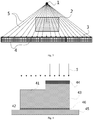
- the radiation source 1 emits the radiation beam 5 to the dual energy detector of the present application to form a beam surface, and the inspected object 2 is disposed in a range covered by the beam surface.
- the dual energy detector includes a detector module mount 3 and a plurality of detector modules 4. The plurality of detector modules 4 are juxtaposedly disposed on the same mounting plane of the detector module mount 3, and the respective various detector modules 4 are oriented parallel to each other.
- the detector modules 4 are more simple in terms of design, installation and debugging on the detector module mount 3, and moreover, the detector module mount 3 is also relatively small in thickness and also relatively light in weight, so that it is also comparatively convenient during the folding or driving of the detector module mount 3.
- a plurality of detector modules 4 are adjacently disposed on the same mounting plane of the detector module mount 3.
- the detector modules 4 are adjacent to each other at an edge position, thereby reducing the scattered light entering the detector modules 4 from the edge position such as to make more smooth transition of the received signals between adjacent detector modules.
- the plurality of the detector modules 4 are arranged on the detector module mount 3 along a linear sequence during design, and such structure only needs to occupy less thickness dimension of the detector module mount 3, and moreover, it is also very convenient during the installation.
- a plurality of the detector modules 4 may also be provided in a plurality of rows on the mounting plane of the detector module mount 3, each row of the detector modules 4 being adjacently disposed in parallel. A plurality of rows of detector modules 4 may effectively improve the scanning speed of the inspected object 2.
- the detector module 4 includes a higher energy detector array 43 and a lower energy detector array 41, and the higher energy detector array 43 and the lower energy detector array 41 may both formed by sequentially arranging a plurality of detector units. Compared with the front-and-rear arrangement of the lower energy detector array and the higher energy detector array in the existing dual energy detector, the higher energy detector array 43 and the lower energy detector array 41 are juxtaposedly provided relative to a same mounting plane of the detector module mount 3.
- the "high energy” and “low energy” detector arrays are relatively defined in the art.
- the radiation beam is a broad energy spectrum structure, in which partial rays with a low energy are easily absorbed by a substance.
- the higher energy detector array relatively absorbs more high energy radiation portions, while the lower energy detector array relatively absorbs more low energy radiation portions.
- the photodiode 46 below the higher energy detector array 43 is substantially in the same plane as the photodiode 42 below the lower energy detector array 41, and the higher energy detector array 43 and the lower energy detector array 41 share the same printed circuit board 45.
- the maximum thickness of the detector module is the thickness of the higher energy detector array 43 (further plus the thickness of the filter 44, if there is a filter 44) plus the thicknesses of the photodiode 46 and the printed circuit board 45.
- the arrangement manner of the existing dual energy detector determines that the thickness of the detector module is at least a sum of the thicknesses of the higher energy detector array a45 and the lower energy detector array a41, further plus the thicknesses of the photodiode and the printed circuit board connected thereto respectively, so that it is apparent that this is considerably greater than the thickness of the detector module in the present application.
- This further determines that there is a small necessary thickness dimension of the detector module mount in the embodiments of the present application, thereby facilitating the installation and use of the dual energy detector of the present application.
- the radiation beam a5 needs to penetrate the lower energy detector array a41 before reaching the higher energy detector array a45.
- Such irradiation line inevitably affects the selection of the performance of the lower energy detector array a41 and the higher energy detector array a45, especially the low-energy detector array a41.
- the radiation beam 5 in the present application may be independently irradiated to the higher energy detector array 41 and the lower energy detector array 43 juxtaposed to each other, which reduces to certain extent the mutual restriction during selection of the higher and lower energy detector arrays. Further, such arrangement manner may also simplify the adjustment of the energy response and sensitivity to the radiation beam between the higher and lower energy detector arrays.
- the higher energy detector array 43 and the lower energy detector array 41 in each of the detector modules 4 are disposed such as to be adjacent to each other.
- the juxtaposed higher and lower energy detector arrays which may effectuate a large sensitive area of the detector, can match the width of the radiation beam, so as to more effectively utilize the width of the radiation beam, and reduce the radiation protection pressure.
- the density of sensitive medium of the higher energy detector array 43 is higher than the density of sensitive medium of the lower energy detector array 41, and/or the effective atomic number of sensitive medium of the higher energy detector array 43 is higher than the effective atomic number of sensitive medium of the lower energy detector array 41.
- the higher energy detector array is made by choosing a sensitive medium of a higher density and/or effective atomic number, such as to reduce the effects of crosstalk when the rays obliquely irradiate the sensitive medium.
- the scintillation efficiency of sensitive medium of the lower energy detector array 41 is higher than the scintillation efficiency of sensitive medium of the higher energy detector array 43, so as to improve the sensitivity of the lower energy detector array 41.
- a filter 44 may be further provided on a front side of the higher energy detector array 43.
- the lower energy detector array 41 does not possess a filtering function of the higher energy detector array, while the filtering function is realized by the filter 44, such that the filtering function may no longer be considered when the sensitive medium of the lower energy detector array 41 is selected, such as to expand the selection range of the sensitive medium of the lower energy detector array 41.
- the higher energy detector array 43 may choose a proper material and dimension of the filter 44 according to own requirements, so that it is more simple in design. After the filter 44 is added, it is preferable that the sum of the thicknesses of the higher energy detector array 43 and the filter 44 is higher than the thickness of the lower energy detector array 41.
- a heavy metal spacer may also be provided between the detector units.
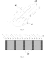
- a heavy metal spacer 47 provided between various detector units constituting the higher and lower energy detector arrays, may effectively reduce the scattered light scattered from an edge of a detector unit to another detector unit adjacent thereto.
- the aforementioned embodiments of various dual energy detectors may be applied to various fields, especially applied to the radiation inspection system. Therefore, the present application also provides a radiation inspection system comprising any one of the foregoing dual energy detectors for effectuating scanned inspection of an inspected object.
Landscapes
- Physics & Mathematics (AREA)
- Life Sciences & Earth Sciences (AREA)
- General Physics & Mathematics (AREA)
- High Energy & Nuclear Physics (AREA)
- Health & Medical Sciences (AREA)
- Spectroscopy & Molecular Physics (AREA)
- Molecular Biology (AREA)
- Geophysics (AREA)
- General Life Sciences & Earth Sciences (AREA)
- Analytical Chemistry (AREA)
- Pathology (AREA)
- Immunology (AREA)
- General Health & Medical Sciences (AREA)
- Biochemistry (AREA)
- Chemical & Material Sciences (AREA)
- Measurement Of Radiation (AREA)
- Analysing Materials By The Use Of Radiation (AREA)
- Light Receiving Elements (AREA)
Abstract
Description
- The present application claims priority from Chinese application number
CN201611205087.1 filed Dec. 23, 2016 - The present application relates to the field of radiation inspection, and in particular relates to a dual energy detector and a radiation inspection system.
- In the existing radiation inspection system, the radiation beam emitted by a radiation source located on one side of a system after passing through a collimator may form a "sector" beam surface. The detector module is located on the other side of the system, and an inspected object is between the radiation beam and the detector module. As shown in
Figure 1 , the radiation beam a5 emitted by the radiation source a1 after penetrating the inspected object a2, is emitted towards a plurality of detector modules a4 on a detector module mount a3. The existing detector module usually consists of certain amount of higher energy and lower energy detector arrays. All the detector modules are oriented towards a radiation source point. - For a dual energy detector, as shown in
Figure 2 , the lower energy detector array a41 and the higher energy detector array a45 are generally provided in a front-and-rear positional relation. Wherein, the lower energy detector array a41 is located on one side proximate to the radiation source a1, while the higher energy detector array a45 is disposed on one side distant from the radiation source a1. The radiation beam a5 penetrates the lower energy detector array a41 before reaching the higher energy detector array a45. The lower energy detector array a41 relatively absorbs more energy of low energy rays, and the higher energy detector array a45 relatively absorbs more high energy rays. Finally, such two signals are analyzed to obtain information of an effective atomic number of an inspected substance. A photodiode a42 and a printed circuit board a43 are provided on a rear side of the lower energy detector array a41, and a photodiode a46 and a printed circuit board a47 are provided on a rear side of the higher energy detector array a45. In use, the lower energy detector array a41, in addition to acquiring the low energy signal, also assumes the filtering function of the higher energy detector array a45 by means of a filter a44. - The structure of this existing dual-energy detector is very universal at present, and in the specific implementation, there are the following problems:
- 1. Each detector module has a fixed orientation at the installation location. The orientation is directed to a target point of the radiation source. The design is relatively complicated and the installation and debugging are very difficult. Moreover, if the overall geometry varies (such as a position of the radiation source), the entire detector module mount needs to be re-designed. Further, in order to stably install the detector module, the detector module mount needs to be made to be relatively thick, so that it is quite inconvenient in terms of installation and use.
- 2. The detector modules are so unsmooth therebetween that, the detector at an edge of an edge module is susceptible to scattering interference.
- 3. The sensitive medium of the lower energy detector array is limited in an optional range, and thus is not a desirable filtering material. For the lower energy detector array, the area of the photodiodes on a rear side thereof may generally be less than the area of the lower energy detector array, but does not match the sensitive area of the lower energy detector.
- 4. In actual use, the width of the radiation beam at the detector module which is difficult to be constrained to the width of a sensitive area of the detector, may generally substantially exceed the width of a single detector array, resulting in an additional radiation protection pressure.
- It is an object of the present application to provide a dual energy detector and a radiation inspection system that facilitates the installation and use of the dual energy detector.
- In order to achieve the aforementioned object, the present application provides a dual energy detector, comprising: a detector module mount and a plurality of detector modules, the detector module including a higher energy detector array and a lower energy detector array, which are juxtaposedly provided on the detector module mount to be independently irradiated.
- Further, the higher energy detector array and the lower energy detector array in each of the detector modules are disposed such as to be adjacent to each other.
- Further, a plurality of the detector modules are adjacently disposed on a same mounting plane of the detector module mount.
- Further, the plurality of the detector modules are arranged on the detector module mount along a linear sequence.
- Further, a plurality of the detector modules are provided in a plurality of rows on the mounting plane of the detector module mount, each row of the detector modules being adjacently disposed in parallel.
- Further, a heavy metal spacer is provided among various detector units included in the higher energy detector array and/or the lower energy detector array.
- Further, a filter is further provided at one side of the higher energy detector array proximate to a radiation source.
- Further, the density of sensitive medium of the higher energy detector array is higher than that of the lower energy detector array, and/or the effective atomic number of sensitive medium of the higher energy detector array is higher than that of the lower energy detector array.
- Further, the scintillation efficiency of sensitive medium of the lower energy detector array is higher than that of the higher energy detector array.
- In order to realize the aforementioned object, the present application provides a radiation inspection system, comprising the aforementioned dual energy detector.
- On the basis of the aforementioned technical solution, the present detector provides the higher and lower energy detector arrays in the detector module relative to the same mounting plane of the detector module mount according to a juxtaposed manner, and such structure may simplify the arrangement of the photodiodes and printed circuit boards to which the higher and lower energy detector arrays are connected, such that necessary thickness dimension of the detector module mount is reduced, thereby facilitating the installation and use of the dual energy detector of the present application. On the other hand, relative to the form that the radiation beam needs to penetrate the lower energy detector array before reaching the higher energy detector array when the existing dual energy detector receives the radiation by the radiation source, the radiation beam in the present application may be independently irradiated to the higher and lower energy detector arrays juxtaposed to each other, which reduces to certain extent the mutual restriction during selection of the higher and lower energy detector arrays.
- The drawings described herein are used to provide a further understanding of the present application and constitute a part of the present application. The illustrative embodiments of the present application as well as the descriptions thereof, which are used for explaining the present application, do not constitute improper definitions on the present application. In the drawings:
-
Figure 1 is a schematic view for the principles of the existing radiation inspection system. -
Figure 2 is a schematic view of the structure of the detector module in the existing dual energy detector. -
Figure 3 is a schematic view for the principles of an embodiment of the radiation inspection system of the present application. -
Figure 4 is a schematic view of the structure of the detector modules in an embodiment of the dual energy detector of the present application. -
Figure 5 is a schematic view of the structure of providing higher and lower energy detector arrays in various detector modules in another embodiment of the dual energy detector of the present application. -
Figure 6 is a schematic view of the structure of providing a heavy metal spacer between various detector units in the higher and lower energy detector arrays in a further embodiment of the dual energy detector of the present application. - Next, the technical solution of the present application is further described in detail by means of the drawings and embodiments.
- As shown in
Figure 3 , it is a schematic view for the principles of an embodiment of the radiation inspection system of the present application. InFigure 3 , theradiation source 1 emits theradiation beam 5 to the dual energy detector of the present application to form a beam surface, and the inspectedobject 2 is disposed in a range covered by the beam surface. The dual energy detector includes adetector module mount 3 and a plurality ofdetector modules 4. The plurality ofdetector modules 4 are juxtaposedly disposed on the same mounting plane of thedetector module mount 3, and the respectivevarious detector modules 4 are oriented parallel to each other. Compared with the structural form that the detector modules of the existing dual energy detector are respectively oriented towards a target point of theradiation source 1, as thevarious detector modules 4 in the present embodiment occupy a small dimension in a thickness direction, thedetector modules 4 are more simple in terms of design, installation and debugging on thedetector module mount 3, and moreover, thedetector module mount 3 is also relatively small in thickness and also relatively light in weight, so that it is also comparatively convenient during the folding or driving of thedetector module mount 3. - In order to reduce the scattering interference to which the edge of the detector modules is subject, it is preferable that a plurality of
detector modules 4 are adjacently disposed on the same mounting plane of thedetector module mount 3. In other words, thedetector modules 4 are adjacent to each other at an edge position, thereby reducing the scattered light entering thedetector modules 4 from the edge position such as to make more smooth transition of the received signals between adjacent detector modules. - In the arrangement manner of the
detector modules 4, it is preferable that the plurality of thedetector modules 4 are arranged on thedetector module mount 3 along a linear sequence during design, and such structure only needs to occupy less thickness dimension of thedetector module mount 3, and moreover, it is also very convenient during the installation. In a further embodiment (as shown inFigure 5 ), a plurality of thedetector modules 4 may also be provided in a plurality of rows on the mounting plane of thedetector module mount 3, each row of thedetector modules 4 being adjacently disposed in parallel. A plurality of rows ofdetector modules 4 may effectively improve the scanning speed of the inspectedobject 2. - With reference to
Figure 4 , thedetector module 4 includes a higherenergy detector array 43 and a lowerenergy detector array 41, and the higherenergy detector array 43 and the lowerenergy detector array 41 may both formed by sequentially arranging a plurality of detector units. Compared with the front-and-rear arrangement of the lower energy detector array and the higher energy detector array in the existing dual energy detector, the higherenergy detector array 43 and the lowerenergy detector array 41 are juxtaposedly provided relative to a same mounting plane of thedetector module mount 3. - It is necessary to explain that the "high energy" and "low energy" detector arrays are relatively defined in the art. In general, the radiation beam is a broad energy spectrum structure, in which partial rays with a low energy are easily absorbed by a substance. Among them, the higher energy detector array relatively absorbs more high energy radiation portions, while the lower energy detector array relatively absorbs more low energy radiation portions.
- In
Figure 4 , thephotodiode 46 below the higherenergy detector array 43 is substantially in the same plane as thephotodiode 42 below the lowerenergy detector array 41, and the higherenergy detector array 43 and the lowerenergy detector array 41 share the same printedcircuit board 45. This results in that the maximum thickness of the detector module is the thickness of the higher energy detector array 43 (further plus the thickness of thefilter 44, if there is a filter 44) plus the thicknesses of thephotodiode 46 and the printedcircuit board 45. Moreover, the arrangement manner of the existing dual energy detector determines that the thickness of the detector module is at least a sum of the thicknesses of the higher energy detector array a45 and the lower energy detector array a41, further plus the thicknesses of the photodiode and the printed circuit board connected thereto respectively, so that it is apparent that this is considerably greater than the thickness of the detector module in the present application. This further determines that there is a small necessary thickness dimension of the detector module mount in the embodiments of the present application, thereby facilitating the installation and use of the dual energy detector of the present application. - Judged from the irradiation line of the radiation source, when the existing detector receives the irradiation by the radiation source, the radiation beam a5 needs to penetrate the lower energy detector array a41 before reaching the higher energy detector array a45. Such irradiation line inevitably affects the selection of the performance of the lower energy detector array a41 and the higher energy detector array a45, especially the low-energy detector array a41. Moreover, in the present embodiment, the
radiation beam 5 in the present application may be independently irradiated to the higherenergy detector array 41 and the lowerenergy detector array 43 juxtaposed to each other, which reduces to certain extent the mutual restriction during selection of the higher and lower energy detector arrays. Further, such arrangement manner may also simplify the adjustment of the energy response and sensitivity to the radiation beam between the higher and lower energy detector arrays. - In order to reduce the scattering interference of the higher
energy detector array 43 and the lowerenergy detector array 41 at an edge position, it is preferable that the higherenergy detector array 43 and the lowerenergy detector array 41 in each of thedetector modules 4 are disposed such as to be adjacent to each other. The juxtaposed higher and lower energy detector arrays which may effectuate a large sensitive area of the detector, can match the width of the radiation beam, so as to more effectively utilize the width of the radiation beam, and reduce the radiation protection pressure. - In selection of the performance of the sensitive medium of the higher and lower energy detector arrays, it is preferable that the density of sensitive medium of the higher
energy detector array 43 is higher than the density of sensitive medium of the lowerenergy detector array 41, and/or the effective atomic number of sensitive medium of the higherenergy detector array 43 is higher than the effective atomic number of sensitive medium of the lowerenergy detector array 41. The higher energy detector array is made by choosing a sensitive medium of a higher density and/or effective atomic number, such as to reduce the effects of crosstalk when the rays obliquely irradiate the sensitive medium. In addition, it is preferable that the scintillation efficiency of sensitive medium of the lowerenergy detector array 41 is higher than the scintillation efficiency of sensitive medium of the higherenergy detector array 43, so as to improve the sensitivity of the lowerenergy detector array 41. - In
Figure 4 , afilter 44 may be further provided on a front side of the higherenergy detector array 43. Compared with the lower energy detector array in the existing dual energy detector which also needs to assume the filtering function of the higher energy detector array, as the lowerenergy detector array 41 is juxtaposedly disposed beside the higherenergy detector array 43, the lowerenergy detector array 41 does not possess a filtering function of the higher energy detector array, while the filtering function is realized by thefilter 44, such that the filtering function may no longer be considered when the sensitive medium of the lowerenergy detector array 41 is selected, such as to expand the selection range of the sensitive medium of the lowerenergy detector array 41. Correspondingly, the higherenergy detector array 43 may choose a proper material and dimension of thefilter 44 according to own requirements, so that it is more simple in design. After thefilter 44 is added, it is preferable that the sum of the thicknesses of the higherenergy detector array 43 and thefilter 44 is higher than the thickness of the lowerenergy detector array 41. - In order to further reduce the scattering between adjacent detector units, a heavy metal spacer may also be provided between the detector units. Take a further embodiment of the dual energy detector of the present application as shown in
Figure 6 for example, inFigure 6 , aheavy metal spacer 47 provided between various detector units constituting the higher and lower energy detector arrays, may effectively reduce the scattered light scattered from an edge of a detector unit to another detector unit adjacent thereto. - The aforementioned embodiments of various dual energy detectors may be applied to various fields, especially applied to the radiation inspection system. Therefore, the present application also provides a radiation inspection system comprising any one of the foregoing dual energy detectors for effectuating scanned inspection of an inspected object.
- Finally, it should be explained that: the aforementioned embodiments are only used to describe the technical solution of the present application rather than limiting the same; although detailed explanations are made to the present application by referring to preferred embodiments, a common technical person in the art should understand that: it is still possible to make amendments to the embodiments of the present application or make equivalent replacements to part of the technical features; without departing from the spirit and scope of the present application, they should all be covered in the scope of the technical solution for which protection is sought in the present application.
Claims (10)
- A dual energy detector, comprising: a detector module mount (3) and a plurality of detector modules (4), said detector module (4) comprising a higher energy detector array (43) and a lower energy detector array (41), which are juxtaposedly provided on said detector module mount (3) to be independently irradiated.
- The dual energy detector according to claim 1, wherein said higher energy detector array (43) and said lower energy detector array (41) in each of said detector modules (4) are disposed to be adjacent to each other.
- The dual energy detector according to claim 1, wherein a plurality of said detector modules (4) are adjacently disposed on a same mounting plane of said detector module mount (3).
- The dual energy detector according to claim 3, wherein the plurality of said detector modules (4) are arranged on said detector module mount (3) along a linear sequence.
- The dual energy detector according to claim 3, wherein a plurality of said detector modules (4) are provided in a plurality of rows on the mounting plane of said detector module mount (3), each row of said detector modules (4) being adjacently disposed in parallel.
- The dual energy detector according to any one of claims 1-5, wherein a heavy metal spacer (47) is provided among various detector units included in said higher energy detector array (43) and/or said lower energy detector array (41).
- The dual energy detector according to any one of claims 1-5, wherein a filter (44) is provided at one side of said higher energy detector array (43) proximate to a radiation source.
- The dual energy detector according to any one of claims 1-5, wherein the density of sensitive medium of said higher energy detector array (43) is higher than that of said lower energy detector array (41), and/or the effective atomic number of sensitive medium of said higher energy detector array (43) is higher than that of said lower energy detector array (41).
- The dual energy detector according to any one of claims 1-5, wherein the scintillation efficiency of sensitive medium of said lower energy detector array (41) is higher than that of said higher energy detector array (43).
- A radiation inspection system, comprising the dual energy detector according to any one of claims 1 to 9.
Applications Claiming Priority (1)
| Application Number | Priority Date | Filing Date | Title |
|---|---|---|---|
| CN201611205087.1A CN106483153A (en) | 2016-12-23 | 2016-12-23 | Dual-energy detector and radiation checking system |
Publications (1)
| Publication Number | Publication Date |
|---|---|
| EP3346293A1 true EP3346293A1 (en) | 2018-07-11 |
Family
ID=58285955
Family Applications (1)
| Application Number | Title | Priority Date | Filing Date |
|---|---|---|---|
| EP17210653.6A Withdrawn EP3346293A1 (en) | 2016-12-23 | 2017-12-27 | Dual energy detector and radiation inspection system |
Country Status (4)
| Country | Link |
|---|---|
| US (1) | US10386502B2 (en) |
| EP (1) | EP3346293A1 (en) |
| JP (1) | JP6687590B2 (en) |
| CN (1) | CN106483153A (en) |
Families Citing this family (17)
| Publication number | Priority date | Publication date | Assignee | Title |
|---|---|---|---|---|
| JP6717784B2 (en) * | 2017-06-30 | 2020-07-08 | アンリツインフィビス株式会社 | Article inspection apparatus and calibration method thereof |
| CN107478664B (en) * | 2017-09-06 | 2020-06-26 | 奕瑞影像科技(太仓)有限公司 | Linear dual-energy X-ray sensor and linear dual-energy X-ray detection system |
| CN108387593A (en) * | 2017-12-12 | 2018-08-10 | 北京航星机器制造有限公司 | A kind of CT detection devices |
| CN109946747A (en) * | 2019-03-25 | 2019-06-28 | 北京航星机器制造有限公司 | A dual-energy CT detection system based on a novel detection device |
| KR102278129B1 (en) * | 2019-12-19 | 2021-07-15 | 오석심 | An x-ray line scanner and the tiling method thereof |
| DE102020113814A1 (en) | 2020-05-22 | 2021-11-25 | minrocon GmbH | Bulk material analysis device, bulk material separation device and methods for analyzing and / or separating bulk materials |
| DE102020117484A1 (en) | 2020-07-02 | 2022-01-05 | Smiths Heimann Gmbh | DUAL ENERGY DETECTOR AND PROCESSING PROCESS FOR DETECTOR DATA |
| ES3066997T3 (en) * | 2020-08-04 | 2026-05-19 | Mettler Toledo Llc | Detector array and apparatus for absorption imaging comprising said detector array |
| CN112704511A (en) * | 2020-12-31 | 2021-04-27 | 北京朗视仪器有限公司 | Method and equipment for measuring bone density through oral cavity cone beam CT |
| CN112603354A (en) * | 2020-12-31 | 2021-04-06 | 北京朗视仪器有限公司 | Method and equipment for measuring density of oral bone |
| CN112704512A (en) * | 2020-12-31 | 2021-04-27 | 北京朗视仪器有限公司 | Method and equipment for measuring bone mineral density through oral panoramic film |
| CN113252714A (en) * | 2021-06-15 | 2021-08-13 | 德瑞科(天津)机械制造有限公司 | Structure and dual-energy CT detector with filtering and anti-scattering |
| CN114397694A (en) * | 2021-12-21 | 2022-04-26 | 上海奕瑞光电子科技股份有限公司 | X-ray dual-energy-spectrum detection linear array detector |
| CN115685303A (en) * | 2022-10-20 | 2023-02-03 | 上海奕瑞光电子科技股份有限公司 | Multi-energy X-ray detector, detection board, imaging system and imaging method |
| CN115855981A (en) * | 2022-12-20 | 2023-03-28 | 上海太易检测技术有限公司 | Dual-energy detector based on side-by-side structure |
| CN118276149A (en) * | 2022-12-26 | 2024-07-02 | 同方威视技术股份有限公司 | Detectors for detecting radiation |
| CN119997633A (en) * | 2024-12-25 | 2025-05-13 | 奕瑞电子科技集团股份有限公司 | X-ray detector and method for manufacturing the same |
Citations (6)
| Publication number | Priority date | Publication date | Assignee | Title |
|---|---|---|---|---|
| US4149081A (en) * | 1976-11-29 | 1979-04-10 | Varian Associates, Inc. | Removal of spectral artifacts and utilization of spectral effects in computerized tomography |
| EP1063538A2 (en) * | 1999-06-23 | 2000-12-27 | The Nottingham Trent University | Linear array scintillator system |
| US20070172027A1 (en) * | 2005-12-31 | 2007-07-26 | Yuanjing Li | Multi-array detector module structure for radiation imaging |
| US20100284515A1 (en) * | 2009-05-08 | 2010-11-11 | Neeraj Agrawal | Apparatus for Bone Density Assessment and Monitoring |
| US20120236987A1 (en) * | 2011-03-18 | 2012-09-20 | David Ruimi | Multiple energy ct scanner |
| EP3029452A1 (en) * | 2013-07-29 | 2016-06-08 | Nuctech Company Limited | Detectors in hash arrangement for x/gamma ray container/vehicle inspection device |
Family Cites Families (17)
| Publication number | Priority date | Publication date | Assignee | Title |
|---|---|---|---|---|
| JPS6271881A (en) * | 1985-09-26 | 1987-04-02 | Toshiba Corp | Radiation detector |
| JPH03273687A (en) * | 1990-03-22 | 1991-12-04 | Matsushita Electric Ind Co Ltd | Radiation absorbent material and radiation detector |
| US5841833A (en) * | 1991-02-13 | 1998-11-24 | Lunar Corporation | Dual-energy x-ray detector providing spatial and temporal interpolation |
| JP2001264495A (en) * | 2000-03-16 | 2001-09-26 | Fuji Photo Film Co Ltd | Radiation energy separation filter, solid-state sensor, radiation image information acquisition device using the same, and radiation image information acquisition method |
| US9113839B2 (en) * | 2003-04-25 | 2015-08-25 | Rapiscon Systems, Inc. | X-ray inspection system and method |
| US7388208B2 (en) * | 2006-01-11 | 2008-06-17 | Ruvin Deych | Dual energy x-ray detector |
| JP5566218B2 (en) * | 2010-08-11 | 2014-08-06 | 株式会社トクヤマ | Fluoride single crystal, vacuum ultraviolet light emitting device, scintillator, and method for producing fluoride single crystal |
| JP6010051B2 (en) * | 2011-02-03 | 2016-10-19 | コーニンクレッカ フィリップス エヌ ヴェKoninklijke Philips N.V. | Single or multi energy vertical radiation sensitive detector array and radiation detection method |
| DE102011053971A1 (en) * | 2011-09-27 | 2013-03-28 | Wipotec Wiege- Und Positioniersysteme Gmbh | Method and device for detecting the structure of moving piece goods, in particular for detecting impurities in liquid or pasty products |
| CA3080221A1 (en) * | 2012-02-14 | 2013-08-22 | American Science And Engineering, Inc. | X-ray inspection using wavelength-shifting fiber-coupled scintillation detectors |
| JP5726271B2 (en) * | 2013-11-08 | 2015-05-27 | 浜松ホトニクス株式会社 | Radiation detection apparatus, radiation image acquisition system, radiation inspection system, and radiation detection method |
| CN104749199B (en) * | 2013-12-30 | 2019-02-19 | 同方威视技术股份有限公司 | Dual-energy/dual-view high-energy X-ray fluoroscopic imaging system |
| JP6274939B2 (en) * | 2014-03-26 | 2018-02-07 | アンリツインフィビス株式会社 | X-ray inspection equipment |
| WO2015167481A1 (en) * | 2014-04-30 | 2015-11-05 | Analogic Corporation | Detector array for imaging modality |
| US10562785B2 (en) * | 2014-09-30 | 2020-02-18 | Hitachi Metals, Ltd. | Fluorescent material, scintillator, scintillator array, and radiation detector |
| CN105510363B (en) * | 2015-12-29 | 2019-05-07 | 同方威视技术股份有限公司 | Dual energy detector device, system and method |
| CN206369708U (en) * | 2016-12-23 | 2017-08-01 | 同方威视技术股份有限公司 | Dual-energy detector and radiation checking system |
-
2016
- 2016-12-23 CN CN201611205087.1A patent/CN106483153A/en active Pending
-
2017
- 2017-12-25 JP JP2017248501A patent/JP6687590B2/en active Active
- 2017-12-26 US US15/853,961 patent/US10386502B2/en active Active
- 2017-12-27 EP EP17210653.6A patent/EP3346293A1/en not_active Withdrawn
Patent Citations (6)
| Publication number | Priority date | Publication date | Assignee | Title |
|---|---|---|---|---|
| US4149081A (en) * | 1976-11-29 | 1979-04-10 | Varian Associates, Inc. | Removal of spectral artifacts and utilization of spectral effects in computerized tomography |
| EP1063538A2 (en) * | 1999-06-23 | 2000-12-27 | The Nottingham Trent University | Linear array scintillator system |
| US20070172027A1 (en) * | 2005-12-31 | 2007-07-26 | Yuanjing Li | Multi-array detector module structure for radiation imaging |
| US20100284515A1 (en) * | 2009-05-08 | 2010-11-11 | Neeraj Agrawal | Apparatus for Bone Density Assessment and Monitoring |
| US20120236987A1 (en) * | 2011-03-18 | 2012-09-20 | David Ruimi | Multiple energy ct scanner |
| EP3029452A1 (en) * | 2013-07-29 | 2016-06-08 | Nuctech Company Limited | Detectors in hash arrangement for x/gamma ray container/vehicle inspection device |
Also Published As
| Publication number | Publication date |
|---|---|
| US20180180746A1 (en) | 2018-06-28 |
| CN106483153A (en) | 2017-03-08 |
| US10386502B2 (en) | 2019-08-20 |
| JP2018105864A (en) | 2018-07-05 |
| JP6687590B2 (en) | 2020-04-22 |
Similar Documents
| Publication | Publication Date | Title |
|---|---|---|
| US10386502B2 (en) | Dual energy detector and radiation inspection system | |
| EP2960686B1 (en) | Detector device, dual energy ct system and detection method using the system | |
| CN209728185U (en) | A kind of block form double energy X-ray detector | |
| WO2004072679A3 (en) | Single photon emission computed tomography system | |
| US9218933B2 (en) | Low-dose radiographic imaging system | |
| RU2009123014A (en) | RADIATION DETECTOR WITH MULTIPLE ELECTRODES ON A SENSITIVE LAYER | |
| CN102109473B (en) | Method for imaging objects through photoneutron transmission and detector array | |
| US20170184515A1 (en) | Dual-energy detection apparatus, system and method | |
| CN102446573A (en) | Hybrid collimator for X-rays and method of making same | |
| WO2011097386A1 (en) | Multiple plane multi-inverse fan-beam detection systems and method for using the same | |
| CN110325846B (en) | Sample inspection apparatus employing diffraction detector | |
| CN107478664B (en) | Linear dual-energy X-ray sensor and linear dual-energy X-ray detection system | |
| US20230380781A1 (en) | X-Ray Detection Structure and System | |
| CN113874758A (en) | Panel radiation detector | |
| CN208314216U (en) | A kind of double energy X-ray detector | |
| CN209280934U (en) | A kind of dual-energy detector and planar detector | |
| CN206369708U (en) | Dual-energy detector and radiation checking system | |
| JP2005308748A (en) | Detector module and detector for detecting X-rays | |
| CN103957804B (en) | The data detection system of X ray CT device and X ray CT device | |
| EP3951436B1 (en) | DETECTOR ORDER AND DEVICE FOR ABSORPTION IMAGING WITH THIS DETECTOR ORDER | |
| WO2009098014A2 (en) | Device and method for recording an image | |
| EP1173856B1 (en) | Method and apparatus for simplified alignment in x-ray imaging | |
| CN208459303U (en) | Transmission checks equipment | |
| US7361902B2 (en) | Radiation detector with a detection field comprising scintillators and photodiodes | |
| US20250052915A1 (en) | X-Ray Detection Structure with a Plurality of Scintillator Volumes in a Spatially Periodic Arrangement |
Legal Events
| Date | Code | Title | Description |
|---|---|---|---|
| PUAI | Public reference made under article 153(3) epc to a published international application that has entered the european phase |
Free format text: ORIGINAL CODE: 0009012 |
|
| 17P | Request for examination filed |
Effective date: 20180117 |
|
| AK | Designated contracting states |
Kind code of ref document: A1 Designated state(s): AL AT BE BG CH CY CZ DE DK EE ES FI FR GB GR HR HU IE IS IT LI LT LU LV MC MK MT NL NO PL PT RO RS SE SI SK SM TR |
|
| AX | Request for extension of the european patent |
Extension state: BA ME |
|
| RBV | Designated contracting states (corrected) |
Designated state(s): AL AT BE BG CH CY CZ DE DK EE ES FI FR GB GR HR HU IE IS IT LI LT LU LV MC MK MT NL NO PL PT RO RS SE SI SK SM TR |
|
| STAA | Information on the status of an ep patent application or granted ep patent |
Free format text: STATUS: THE APPLICATION HAS BEEN WITHDRAWN |
|
| 18W | Application withdrawn |
Effective date: 20210112 |