EP3344802B1 - Elektroplattierungsprozessor mit schirmelektrode - Google Patents
Elektroplattierungsprozessor mit schirmelektrode Download PDFInfo
- Publication number
- EP3344802B1 EP3344802B1 EP16842572.6A EP16842572A EP3344802B1 EP 3344802 B1 EP3344802 B1 EP 3344802B1 EP 16842572 A EP16842572 A EP 16842572A EP 3344802 B1 EP3344802 B1 EP 3344802B1
- Authority
- EP
- European Patent Office
- Prior art keywords
- membrane
- thiefolyte
- processor
- isolyte
- thief
- Prior art date
- Legal status (The legal status is an assumption and is not a legal conclusion. Google has not performed a legal analysis and makes no representation as to the accuracy of the status listed.)
- Active
Links
Images


Classifications
-
- C—CHEMISTRY; METALLURGY
- C25—ELECTROLYTIC OR ELECTROPHORETIC PROCESSES; APPARATUS THEREFOR
- C25D—PROCESSES FOR THE ELECTROLYTIC OR ELECTROPHORETIC PRODUCTION OF COATINGS; ELECTROFORMING; APPARATUS THEREFOR
- C25D21/00—Processes for servicing or operating cells for electrolytic coating
- C25D21/12—Process control or regulation
-
- C—CHEMISTRY; METALLURGY
- C25—ELECTROLYTIC OR ELECTROPHORETIC PROCESSES; APPARATUS THEREFOR
- C25D—PROCESSES FOR THE ELECTROLYTIC OR ELECTROPHORETIC PRODUCTION OF COATINGS; ELECTROFORMING; APPARATUS THEREFOR
- C25D17/00—Constructional parts, or assemblies thereof, of cells for electrolytic coating
- C25D17/001—Apparatus specially adapted for electrolytic coating of wafers, e.g. semiconductors or solar cells
-
- C—CHEMISTRY; METALLURGY
- C25—ELECTROLYTIC OR ELECTROPHORETIC PROCESSES; APPARATUS THEREFOR
- C25D—PROCESSES FOR THE ELECTROLYTIC OR ELECTROPHORETIC PRODUCTION OF COATINGS; ELECTROFORMING; APPARATUS THEREFOR
- C25D17/00—Constructional parts, or assemblies thereof, of cells for electrolytic coating
- C25D17/002—Cell separation, e.g. membranes, diaphragms
-
- C—CHEMISTRY; METALLURGY
- C25—ELECTROLYTIC OR ELECTROPHORETIC PROCESSES; APPARATUS THEREFOR
- C25D—PROCESSES FOR THE ELECTROLYTIC OR ELECTROPHORETIC PRODUCTION OF COATINGS; ELECTROFORMING; APPARATUS THEREFOR
- C25D17/00—Constructional parts, or assemblies thereof, of cells for electrolytic coating
- C25D17/007—Current directing devices
-
- C—CHEMISTRY; METALLURGY
- C25—ELECTROLYTIC OR ELECTROPHORETIC PROCESSES; APPARATUS THEREFOR
- C25D—PROCESSES FOR THE ELECTROLYTIC OR ELECTROPHORETIC PRODUCTION OF COATINGS; ELECTROFORMING; APPARATUS THEREFOR
- C25D17/00—Constructional parts, or assemblies thereof, of cells for electrolytic coating
- C25D17/10—Electrodes, e.g. composition, counter electrode
- C25D17/12—Shape or form
-
- C—CHEMISTRY; METALLURGY
- C25—ELECTROLYTIC OR ELECTROPHORETIC PROCESSES; APPARATUS THEREFOR
- C25D—PROCESSES FOR THE ELECTROLYTIC OR ELECTROPHORETIC PRODUCTION OF COATINGS; ELECTROFORMING; APPARATUS THEREFOR
- C25D7/00—Electroplating characterised by the article coated
- C25D7/12—Semiconductors
Definitions
- a current thief electrode also referred to as an auxiliary cathode, is used to better control the plating thickness at the edge of the wafer and for control of the terminal effect on thin seed layers.
- the terminal effect for a given seed layer increases as the electrical conductivity of the electrolyte bath increases.
- a current thief electrode can be effectively used with thinner seed layers combined with high conductivity electrolyte baths.
- the use of thin seed layers is increasing common with redistribution layer (RDL) and wafer level packaging (WLP) plated wafers. For example, it is expected that RDL wafers may soon have copper seed layers as thin as 500A-1000A and copper bath conductivities of 470 mS/cm or higher.
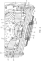
- a thieving secondary cathode 115 resides in its own chamber filled with electrolyte and is in ionic communication with electrolyte in the cathode chamber.
- An auxiliary electrode chamber is defined by the sidewall of the apparatus on one side, by an ionic current collimator on the bottom and on the other side and by a cationic membrane on top. The membrane resides directly above an auxiliary electrode, so that a chamber is formed.
- the amp-minutes involved in processing RDL and WLP wafers can be 20 to 40 times higher than for damascene.
- the wire in a membrane tube thief electrode used in damascene electroplating may not suitable for electroplating RDL and WLP wafers, due to excessive metal plating onto the thief electrode wire, and excessive consumption of thiefolyte. Accordingly, engineering challenges remain in designing apparatus and methods for electroplating RDL and WLP wafers, and other applications, using a thief electrode.
- the virtual annular thief has a diameter greater than 310 mm, for example, 320, 330, 340 or 350 mm.
- the virtual thief electrode is created by placing the thief source near or at the chamber centerline, so that thief current flows radially outward and up to the level of the wafer.
- one or more second anodes 82 in an outer anode compartment are also provided in the form of an inert anode wire in a membrane tube.
- the anodes Flow diffusers 78 and 84 may be used, with the anode tubes on the outlet side of the diffusers. The diffusers may have tabs for holding the membrane tubes down against the floor of the anode compartment.
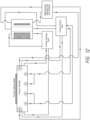
- the catholyte chamber holds a liquid electrolyte, referred to as catholyte.
- a solution of sulfuric acid and deionized water referred to as anolyte
- the circulating anolyte sweeps oxygen evolved off the inert anode wires within the tubes.
- the anolyte also provides a conductive path for the electric field from the inert anode wire to the catholyte.
- the catholyte 202 in the channels 102 conducts the electric field created by the current thief electrode assembly 92 to the virtual thief position 99. In this way, the current thief electrode assembly 92 simulates having an annular thief electrode near the top of the vessel assembly 50.
- Fig. 5-7 show embodiments of thief electrodes.
- the electric current flowing through the thief electrode wire 94 is relatively small compared to the wafer current (1-20%), i.e., the current flowing from the anodes 76 and 82 through the catholyte 202 to the wafer 200.
- the current thief electrode assembly 92 may use a small electrode and membrane area.
- the current thief electrode assembly 92 may be provided in varying shapes, other than annular.
- the current thief electrode assembly 92 may be provided as a platinum wire that is 2.5 to 10 cm long.
- a circumferential wire-in-a-tube thief electrode as used in existing electroplating processors is approximately 100 cm long.
- the thief electrode wire 94 extends through a flat membrane 95A.
- the thief electrode wire 94 is within a membrane tube 95B.
- the thief electrode wire 94 is replaced by a metal plate or disk 97 is within a membrane cover 95C.
- the thief electrode wire 94 or thief disk 97 is electrically connected to an auxiliary cathode.
- Metal mesh may be used in place of the thief electrode wire 94 or the thief disk 97.
- the isolyte 110 is also the anolyte solution flowing through the membrane tubes of the anodes 76 and 84, some of the copper ions that get into the anolyte/isolation solution will pass through the anode membrane tubes and back into the catholyte 202. Furthermore, by greatly reducing the amount of copper transported into the thiefolyte 104, the thiefolyte 104 may be recirculated rather than used only once. Recirculating the thiefolyte 104 greatly reduces processing costs compared to using the thiefolyte only once as is done with damascene wafer processors. The small amount of copper that does make it to the thiefolyte 104 may plate onto the thief electrode wire 94, but only in small amounts that can be quickly deplated between wafers.
- the fluid compartments illustrated in Fig. 8 can be small so that the fluid turnover is high. In the thiefolyte 104, this turnover sweeps hydrogen bubbles out of the fluid volume.
- the isolyte 110 (which may also be the anolyte) and the thiefolyte 104 may be replaced on a bleed and feed schedule. Large quantities may be economically replaced because of the low cost of sulfuric acid and deionized water solutions. As the volumes of the isolyte 110 and thiefolyte 104 are low, less solution is sent to drain compared to single use thiefolyte.
- Fig. 9 shows a design similar to Fig. 8 , with an inner membrane tube 106A within an outer membrane tube 106B, to form an isolation flow path 108.
- a single membrane 100 may be used, with the thiefolyte 104 flowing through an electrowinning cell or channel 120 to remove any metal getting into the thiefolyte across the membrane 100.
- the electrowinning electrode involves maintenance to remove plated on metal build up, but this electrode may be centralized for all the chambers on the thiefolyte fluid loop. This configuration may be used without the electrowinning cell or channel 120, but with the membrane 100 being a monovalent type or anionic type membrane.
- the apparatus and methods described provide a current thieving technique for plating WLP wafers, while overcoming the maintenance issue of copper plate-up on the thief electrode.
- This may be achieved by a two-membrane stack using cationic membranes and high conductivity (low pH) electrolytes.
- the copper containing catholyte is separated from a low-copper isolyte by a cationic membrane, which in turn is separated from the lower-copper thiefolyte by another cationic membrane.
- the thief electrode resides within the thiefolyte. The combination of chemistries and membranes resists migration of copper ions to the thief electrode.
- This two-membrane design with the thief electrode separated from the catholyte in the vessel by two membranes and two electrolytes, is suitable for preventing copper build on the thief electrode during long amp-minute wafer level packaging electroplating.
- the two separating electrolytes can be the same conductive fluid (i.e. acid and water).
- the two separating membranes can be cation or monovalent membranes.
- the separating isolyte and thiefolyte chambers can be formed as a stack with planar membranes, or the two membranes can be formed using co-axial tubular membranes with the inner tube membrane containing the thiefolyte and a wire thief electrode.
- the thief assembly mid -compartment can be the same electrolyte as the anolyte flowing over inert anodes within the process chamber.
- a centrally located thief acts circumferentially, beyond the edge of the wafer though a virtual anode channel. Since the thief current is relatively small compared to the anode currents, it is adequate to have a small, centrally located thief electrode (and its associated structure) rather than a thief electrode or assembly equal to or greater the circumference of the wafer as in currently used processor designs.
- the virtual thief position or opening 99 may be below the wafer plane as shown in Fig 3-4 .
- the virtual thief position 99 may be at or above the wafer plane.
- the virtual thief position or opening 99 may be provided as a continuous annular opening, a segmented opening, or as one or more arcs.
- a virtual thief position or opening 99 may subtend an arc of 30 degrees, so that the current thief acts over only a relatively small sector of the wafer.
- This design may be useful of non-symmetry edge control in a location like a notch, or for processors not having sufficient room for a circumferential current thief opening. In these designs, if the wafer rotates during processing, the current thieving at the edge of the wafer averages out over the entire circumference of the wafer.
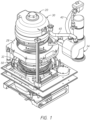
- the electroplating processor has a vessel holding a catholyte containing metal ions, and a head having a wafer holder, with the head movable to position the wafer holder in the vessel, and one or more anodes in the vessel.
- a first electrolyte or thiefolyte compartment contains a first electrolyte or thiefolyte, with the thiefolyte separated from a second electrolyte or isolyte by a first membrane.
- An electric current thief electrode is located in the thiefolyte compartment and is connected to an auxiliary cathode.
Landscapes
- Chemical & Material Sciences (AREA)
- Engineering & Computer Science (AREA)
- Chemical Kinetics & Catalysis (AREA)
- Electrochemistry (AREA)
- Materials Engineering (AREA)
- Metallurgy (AREA)
- Organic Chemistry (AREA)
- Life Sciences & Earth Sciences (AREA)
- Sustainable Development (AREA)
- Automation & Control Theory (AREA)
- Electroplating Methods And Accessories (AREA)
- Electrodes Of Semiconductors (AREA)
- Physics & Mathematics (AREA)
- Condensed Matter Physics & Semiconductors (AREA)
- General Physics & Mathematics (AREA)
- Manufacturing & Machinery (AREA)
- Computer Hardware Design (AREA)
- Microelectronics & Electronic Packaging (AREA)
- Power Engineering (AREA)
- Weting (AREA)
- Electrolytic Production Of Non-Metals, Compounds, Apparatuses Therefor (AREA)
Claims (8)
- Galvanisierungs-Prozessor (20), umfassend:einen Behälter, der einen ersten Elektrolyten enthält, der ein Metallionen enthaltender Katholyt (202) ist;einen Kopf (30) mit einem Waferhalter, wobei der Kopf beweglich ist, um den Waferhalter in dem Behälter zu positionieren;mindestens eine Anode (76, 82) in dem Behälter;ein Isolierelektrolyt-Kompartiment, das einen zweiten Elektrolyten enthält, der ein Isolierelektrolyt (110) ist, der eine Isolierlösung bereitstellt, wobei der Isolierelektrolyt von dem Katholyten durch eine erste Membran (100B) getrennt ist;ein Diebelektrolyt-Kompartiment, das einen dritten Elektrolyten für eine Stromdieb-Elektrodenanordnung enthält und ein Diebelektrolyt ist, wobei der Diebelektrolyt durch eine zweite Membran (100A) von dem Isolierelektrolyt getrennt ist, wobei der Isolierelektrolyt und der Diebelektrolyt aus Säure und Wasser bestehen, wobei die erste und die zweite Membran so konfiguriert sind, dass sie verhindern, dass Metallionen von dem Katholyten in den Diebelektrolyten gelangen; undeine Stromdieb-Elektrode (94) in dem Diebelektrolyt-Kompartiment, wobei die Stromdieb-Elektrode (94) mit einer Hilfskathode verbunden ist und so konfiguriert ist, dass sie während des Galvanisierens eine Stromdieb-Funktion bereitstellt.
- Prozessor nach Anspruch 1, wobei die erste Membran (100A) und/oder die zweite Membran (100B) eine Kationenmembran oder eine monovalente Membran umfasst.
- Prozessor nach Anspruch 1, wobei die Anode (76, 82) einen Draht in einem Membranrohr umfasst, das einen Anolyten enthält, wobei der Anolyt und der Isolierelektrolyt derselbe Elektrolyt sind.
- Prozessor nach Anspruch 1, umfassend eine innere Anode (76), die von einer äußeren Anode (82) umgeben ist, und wobei jede Anode einen Draht in einem Membranrohr umfasst, das einen Anolyten enthält.
- Prozessor nach Anspruch 1, ferner umfassend eine Nachfüllzelle (140), die mit dem Behälter verbunden ist, um Metallionen im Katholyten zu ersetzen, wobei die Nachfüllzelle auch mit einem Anolyt-Kompartiment und dem Isolierelektrolyt-Kompartiment verbunden ist.
- Prozessor nach Anspruch 1, wobei die zweite Membran eine Membranröhre (95B) umfasst.
- Prozessor nach Anspruch 1, der ferner einen Innenring (64) zwischen der mindestens einen Anode und dem Waferhalter umfasst, wobei der Innenring eine obere Fläche (66) aufweist, die sich nach unten zu einer zentralen Öffnung des Innenrings krümmt, und wobei der Innenring eine Vielzahl von vertikalen Durchgangsöffnungen (68) aufweist.
- Prozessor nach Anspruch 1, wobei sich das Isolierelektrolyt-Kompartiment auf einer äußeren Bodenfläche des Behälters befindet.
Applications Claiming Priority (2)
| Application Number | Priority Date | Filing Date | Title |
|---|---|---|---|
| US14/843,803 US9765443B2 (en) | 2015-09-02 | 2015-09-02 | Electroplating processor with current thief electrode |
| PCT/US2016/047586 WO2017040054A1 (en) | 2015-09-02 | 2016-08-18 | Electroplating processor with current thief electrode |
Publications (3)
| Publication Number | Publication Date |
|---|---|
| EP3344802A1 EP3344802A1 (de) | 2018-07-11 |
| EP3344802A4 EP3344802A4 (de) | 2019-05-22 |
| EP3344802B1 true EP3344802B1 (de) | 2025-04-16 |
Family
ID=58098263
Family Applications (1)
| Application Number | Title | Priority Date | Filing Date |
|---|---|---|---|
| EP16842572.6A Active EP3344802B1 (de) | 2015-09-02 | 2016-08-18 | Elektroplattierungsprozessor mit schirmelektrode |
Country Status (6)
| Country | Link |
|---|---|
| US (1) | US9765443B2 (de) |
| EP (1) | EP3344802B1 (de) |
| KR (1) | KR102193172B1 (de) |
| CN (2) | CN106480491B (de) |
| TW (2) | TWM541474U (de) |
| WO (1) | WO2017040054A1 (de) |
Families Citing this family (11)
| Publication number | Priority date | Publication date | Assignee | Title |
|---|---|---|---|---|
| US9765443B2 (en) * | 2015-09-02 | 2017-09-19 | Applied Materials, Inc. | Electroplating processor with current thief electrode |
| SG11202001659PA (en) * | 2017-08-30 | 2020-03-30 | Acm Research Shanghai Inc | Plating apparatus |
| US10494731B2 (en) | 2017-12-11 | 2019-12-03 | Applied Materials, Inc. | Electroplating dynamic edge control |
| CN110512248B (zh) * | 2018-05-21 | 2022-04-12 | 盛美半导体设备(上海)股份有限公司 | 电镀设备及电镀方法 |
| TWI835872B (zh) | 2018-10-03 | 2024-03-21 | 美商蘭姆研究公司 | 用於惰性陽極鍍覆槽的流量分配設備 |
| TWI810250B (zh) * | 2019-02-27 | 2023-08-01 | 大陸商盛美半導體設備(上海)股份有限公司 | 電鍍裝置 |
| JP7256708B2 (ja) * | 2019-07-09 | 2023-04-12 | 株式会社荏原製作所 | めっき装置 |
| US11268208B2 (en) | 2020-05-08 | 2022-03-08 | Applied Materials, Inc. | Electroplating system |
| US11697887B2 (en) * | 2020-10-23 | 2023-07-11 | Applied Materials, Inc. | Multi-compartment electrochemical replenishment cell |
| CN115142104B (zh) * | 2022-07-28 | 2024-04-26 | 福州一策仪器有限公司 | 电镀装置、多通道电镀装置组和电镀反应系统 |
| CN115896904B (zh) * | 2023-03-09 | 2023-05-30 | 苏州智程半导体科技股份有限公司 | 一种晶圆电镀腔室结构 |
Family Cites Families (17)
| Publication number | Priority date | Publication date | Assignee | Title |
|---|---|---|---|---|
| DE19539865A1 (de) * | 1995-10-26 | 1997-04-30 | Lea Ronal Gmbh | Durchlauf-Galvanikanlage |
| US6228231B1 (en) | 1997-05-29 | 2001-05-08 | International Business Machines Corporation | Electroplating workpiece fixture having liquid gap spacer |
| US6004440A (en) * | 1997-09-18 | 1999-12-21 | Semitool, Inc. | Cathode current control system for a wafer electroplating apparatus |
| US8308931B2 (en) * | 2006-08-16 | 2012-11-13 | Novellus Systems, Inc. | Method and apparatus for electroplating |
| US8475636B2 (en) * | 2008-11-07 | 2013-07-02 | Novellus Systems, Inc. | Method and apparatus for electroplating |
| US20050145499A1 (en) * | 2000-06-05 | 2005-07-07 | Applied Materials, Inc. | Plating of a thin metal seed layer |
| US7854828B2 (en) | 2006-08-16 | 2010-12-21 | Novellus Systems, Inc. | Method and apparatus for electroplating including remotely positioned second cathode |
| US20040134775A1 (en) * | 2002-07-24 | 2004-07-15 | Applied Materials, Inc. | Electrochemical processing cell |
| US20070144912A1 (en) * | 2003-07-01 | 2007-06-28 | Woodruff Daniel J | Linearly translating agitators for processing microfeature workpieces, and associated methods |
| TW200641189A (en) | 2005-02-25 | 2006-12-01 | Applied Materials Inc | Counter electrode encased in cation exchange membrane tube for electroplating cell |
| US8784618B2 (en) | 2010-08-19 | 2014-07-22 | International Business Machines Corporation | Working electrode design for electrochemical processing of electronic components |
| US9017528B2 (en) * | 2011-04-14 | 2015-04-28 | Tel Nexx, Inc. | Electro chemical deposition and replenishment apparatus |
| US8496790B2 (en) * | 2011-05-18 | 2013-07-30 | Applied Materials, Inc. | Electrochemical processor |
| US8496789B2 (en) * | 2011-05-18 | 2013-07-30 | Applied Materials, Inc. | Electrochemical processor |
| US9909228B2 (en) | 2012-11-27 | 2018-03-06 | Lam Research Corporation | Method and apparatus for dynamic current distribution control during electroplating |
| US20140367264A1 (en) | 2013-06-18 | 2014-12-18 | Applied Materials, Inc. | Automatic in-situ control of an electro-plating processor |
| US9765443B2 (en) * | 2015-09-02 | 2017-09-19 | Applied Materials, Inc. | Electroplating processor with current thief electrode |
-
2015
- 2015-09-02 US US14/843,803 patent/US9765443B2/en active Active
-
2016
- 2016-08-18 KR KR1020187009356A patent/KR102193172B1/ko active Active
- 2016-08-18 WO PCT/US2016/047586 patent/WO2017040054A1/en not_active Ceased
- 2016-08-18 EP EP16842572.6A patent/EP3344802B1/de active Active
- 2016-08-31 CN CN201610797835.3A patent/CN106480491B/zh active Active
- 2016-08-31 CN CN201621032850.0U patent/CN206204466U/zh not_active Withdrawn - After Issue
- 2016-09-01 TW TW105213438U patent/TWM541474U/zh unknown
- 2016-09-01 TW TW105128222A patent/TWI686512B/zh active
Non-Patent Citations (1)
| Title |
|---|
| LI SHICHENG ET AL: "Concurrently Fabricating Precision Meso- and Microscale Cross-Scale Arrayed Metal Features and Components by Using Wire-Anode Scanning Electroforming Technique", SCHOOL OF MECHANICAL AND POWER ENGINEERING, HENAN POLYTECHNIC UNIVERSITY, JIAOZUO 454000, CHINA, vol. 14, no. 5, 29 April 2023 (2023-04-29), pages 979, XP093057413, DOI: 10.3390/mi14050979 * |
Also Published As
| Publication number | Publication date |
|---|---|
| CN106480491A (zh) | 2017-03-08 |
| KR102193172B1 (ko) | 2020-12-18 |
| CN106480491B (zh) | 2020-10-16 |
| EP3344802A4 (de) | 2019-05-22 |
| US20170058424A1 (en) | 2017-03-02 |
| TWM541474U (zh) | 2017-05-11 |
| WO2017040054A1 (en) | 2017-03-09 |
| TWI686512B (zh) | 2020-03-01 |
| US9765443B2 (en) | 2017-09-19 |
| CN206204466U (zh) | 2017-05-31 |
| TW201718955A (zh) | 2017-06-01 |
| KR20180038062A (ko) | 2018-04-13 |
| EP3344802A1 (de) | 2018-07-11 |
Similar Documents
| Publication | Publication Date | Title |
|---|---|---|
| EP3344802B1 (de) | Elektroplattierungsprozessor mit schirmelektrode | |
| KR102216393B1 (ko) | 합금 도금 시스템에서 패시베이션으로부터 애노드 보호 | |
| TWI697587B (zh) | 藉由使用遠程電流之電鍍均勻性的動態控制設備及方法 | |
| CN205954137U (zh) | 电镀系统 | |
| US8496789B2 (en) | Electrochemical processor | |
| US9920448B2 (en) | Inert anode electroplating processor and replenisher with anionic membranes | |
| CN217948322U (zh) | 电镀系统 | |
| TWI551729B (zh) | 用以控制電鍍槽中之電流密度的具有複數可切換的導電元件之不溶性陽極 | |
| TWI872379B (zh) | 半導體處理之方法 | |
| TW202248466A (zh) | 用於電鍍期間之特定流體動力學的空間及尺寸上非均勻之通道板 |
Legal Events
| Date | Code | Title | Description |
|---|---|---|---|
| STAA | Information on the status of an ep patent application or granted ep patent |
Free format text: STATUS: THE INTERNATIONAL PUBLICATION HAS BEEN MADE |
|
| PUAI | Public reference made under article 153(3) epc to a published international application that has entered the european phase |
Free format text: ORIGINAL CODE: 0009012 |
|
| STAA | Information on the status of an ep patent application or granted ep patent |
Free format text: STATUS: REQUEST FOR EXAMINATION WAS MADE |
|
| 17P | Request for examination filed |
Effective date: 20180302 |
|
| AK | Designated contracting states |
Kind code of ref document: A1 Designated state(s): AL AT BE BG CH CY CZ DE DK EE ES FI FR GB GR HR HU IE IS IT LI LT LU LV MC MK MT NL NO PL PT RO RS SE SI SK SM TR |
|
| AX | Request for extension of the european patent |
Extension state: BA ME |
|
| DAV | Request for validation of the european patent (deleted) | ||
| DAX | Request for extension of the european patent (deleted) | ||
| A4 | Supplementary search report drawn up and despatched |
Effective date: 20190426 |
|
| RIC1 | Information provided on ipc code assigned before grant |
Ipc: C25D 5/16 20060101ALI20190418BHEP Ipc: C25D 17/10 20060101ALI20190418BHEP Ipc: C25D 17/12 20060101ALI20190418BHEP Ipc: C25D 17/06 20060101ALI20190418BHEP Ipc: C25D 7/12 20060101ALI20190418BHEP Ipc: H01L 21/288 20060101ALI20190418BHEP Ipc: C25D 17/00 20060101AFI20190418BHEP |
|
| STAA | Information on the status of an ep patent application or granted ep patent |
Free format text: STATUS: EXAMINATION IS IN PROGRESS |
|
| 17Q | First examination report despatched |
Effective date: 20220105 |
|
| GRAP | Despatch of communication of intention to grant a patent |
Free format text: ORIGINAL CODE: EPIDOSNIGR1 |
|
| STAA | Information on the status of an ep patent application or granted ep patent |
Free format text: STATUS: GRANT OF PATENT IS INTENDED |
|
| RAP3 | Party data changed (applicant data changed or rights of an application transferred) |
Owner name: APPLIED MATERIALS, INC. |
|
| INTG | Intention to grant announced |
Effective date: 20241211 |
|
| GRAS | Grant fee paid |
Free format text: ORIGINAL CODE: EPIDOSNIGR3 |
|
| GRAA | (expected) grant |
Free format text: ORIGINAL CODE: 0009210 |
|
| STAA | Information on the status of an ep patent application or granted ep patent |
Free format text: STATUS: THE PATENT HAS BEEN GRANTED |
|
| P01 | Opt-out of the competence of the unified patent court (upc) registered |
Free format text: CASE NUMBER: APP_7476/2025 Effective date: 20250213 |
|
| AK | Designated contracting states |
Kind code of ref document: B1 Designated state(s): AL AT BE BG CH CY CZ DE DK EE ES FI FR GB GR HR HU IE IS IT LI LT LU LV MC MK MT NL NO PL PT RO RS SE SI SK SM TR |
|
| REG | Reference to a national code |
Ref country code: GB Ref legal event code: FG4D |
|
| REG | Reference to a national code |
Ref country code: CH Ref legal event code: EP Ref country code: DE Ref legal event code: R096 Ref document number: 602016091940 Country of ref document: DE |
|
| REG | Reference to a national code |
Ref country code: IE Ref legal event code: FG4D |
|
| REG | Reference to a national code |
Ref country code: NL Ref legal event code: MP Effective date: 20250416 |
|
| PG25 | Lapsed in a contracting state [announced via postgrant information from national office to epo] |
Ref country code: NL Free format text: LAPSE BECAUSE OF FAILURE TO SUBMIT A TRANSLATION OF THE DESCRIPTION OR TO PAY THE FEE WITHIN THE PRESCRIBED TIME-LIMIT Effective date: 20250416 |
|
| REG | Reference to a national code |
Ref country code: AT Ref legal event code: MK05 Ref document number: 1785718 Country of ref document: AT Kind code of ref document: T Effective date: 20250416 |
|
| PG25 | Lapsed in a contracting state [announced via postgrant information from national office to epo] |
Ref country code: FI Free format text: LAPSE BECAUSE OF FAILURE TO SUBMIT A TRANSLATION OF THE DESCRIPTION OR TO PAY THE FEE WITHIN THE PRESCRIBED TIME-LIMIT Effective date: 20250416 Ref country code: ES Free format text: LAPSE BECAUSE OF FAILURE TO SUBMIT A TRANSLATION OF THE DESCRIPTION OR TO PAY THE FEE WITHIN THE PRESCRIBED TIME-LIMIT Effective date: 20250416 Ref country code: PT Free format text: LAPSE BECAUSE OF FAILURE TO SUBMIT A TRANSLATION OF THE DESCRIPTION OR TO PAY THE FEE WITHIN THE PRESCRIBED TIME-LIMIT Effective date: 20250818 |
|
| PGFP | Annual fee paid to national office [announced via postgrant information from national office to epo] |
Ref country code: DE Payment date: 20250724 Year of fee payment: 10 |
|
| REG | Reference to a national code |
Ref country code: LT Ref legal event code: MG9D |
|
| PG25 | Lapsed in a contracting state [announced via postgrant information from national office to epo] |
Ref country code: NO Free format text: LAPSE BECAUSE OF FAILURE TO SUBMIT A TRANSLATION OF THE DESCRIPTION OR TO PAY THE FEE WITHIN THE PRESCRIBED TIME-LIMIT Effective date: 20250716 Ref country code: GR Free format text: LAPSE BECAUSE OF FAILURE TO SUBMIT A TRANSLATION OF THE DESCRIPTION OR TO PAY THE FEE WITHIN THE PRESCRIBED TIME-LIMIT Effective date: 20250717 |
|
| PG25 | Lapsed in a contracting state [announced via postgrant information from national office to epo] |
Ref country code: PL Free format text: LAPSE BECAUSE OF FAILURE TO SUBMIT A TRANSLATION OF THE DESCRIPTION OR TO PAY THE FEE WITHIN THE PRESCRIBED TIME-LIMIT Effective date: 20250416 |
|
| PG25 | Lapsed in a contracting state [announced via postgrant information from national office to epo] |
Ref country code: BG Free format text: LAPSE BECAUSE OF FAILURE TO SUBMIT A TRANSLATION OF THE DESCRIPTION OR TO PAY THE FEE WITHIN THE PRESCRIBED TIME-LIMIT Effective date: 20250416 |
|
| PG25 | Lapsed in a contracting state [announced via postgrant information from national office to epo] |
Ref country code: HR Free format text: LAPSE BECAUSE OF FAILURE TO SUBMIT A TRANSLATION OF THE DESCRIPTION OR TO PAY THE FEE WITHIN THE PRESCRIBED TIME-LIMIT Effective date: 20250416 |
|
| PG25 | Lapsed in a contracting state [announced via postgrant information from national office to epo] |
Ref country code: AT Free format text: LAPSE BECAUSE OF FAILURE TO SUBMIT A TRANSLATION OF THE DESCRIPTION OR TO PAY THE FEE WITHIN THE PRESCRIBED TIME-LIMIT Effective date: 20250416 |
|
| PG25 | Lapsed in a contracting state [announced via postgrant information from national office to epo] |
Ref country code: RS Free format text: LAPSE BECAUSE OF FAILURE TO SUBMIT A TRANSLATION OF THE DESCRIPTION OR TO PAY THE FEE WITHIN THE PRESCRIBED TIME-LIMIT Effective date: 20250716 |
|
| PG25 | Lapsed in a contracting state [announced via postgrant information from national office to epo] |
Ref country code: IS Free format text: LAPSE BECAUSE OF FAILURE TO SUBMIT A TRANSLATION OF THE DESCRIPTION OR TO PAY THE FEE WITHIN THE PRESCRIBED TIME-LIMIT Effective date: 20250816 |
|
| PG25 | Lapsed in a contracting state [announced via postgrant information from national office to epo] |
Ref country code: LV Free format text: LAPSE BECAUSE OF FAILURE TO SUBMIT A TRANSLATION OF THE DESCRIPTION OR TO PAY THE FEE WITHIN THE PRESCRIBED TIME-LIMIT Effective date: 20250416 |
|
| PG25 | Lapsed in a contracting state [announced via postgrant information from national office to epo] |
Ref country code: SM Free format text: LAPSE BECAUSE OF FAILURE TO SUBMIT A TRANSLATION OF THE DESCRIPTION OR TO PAY THE FEE WITHIN THE PRESCRIBED TIME-LIMIT Effective date: 20250416 Ref country code: DK Free format text: LAPSE BECAUSE OF FAILURE TO SUBMIT A TRANSLATION OF THE DESCRIPTION OR TO PAY THE FEE WITHIN THE PRESCRIBED TIME-LIMIT Effective date: 20250416 |
|
| PG25 | Lapsed in a contracting state [announced via postgrant information from national office to epo] |
Ref country code: CZ Free format text: LAPSE BECAUSE OF FAILURE TO SUBMIT A TRANSLATION OF THE DESCRIPTION OR TO PAY THE FEE WITHIN THE PRESCRIBED TIME-LIMIT Effective date: 20250416 |
|
| PG25 | Lapsed in a contracting state [announced via postgrant information from national office to epo] |
Ref country code: EE Free format text: LAPSE BECAUSE OF FAILURE TO SUBMIT A TRANSLATION OF THE DESCRIPTION OR TO PAY THE FEE WITHIN THE PRESCRIBED TIME-LIMIT Effective date: 20250416 |
|
| PG25 | Lapsed in a contracting state [announced via postgrant information from national office to epo] |
Ref country code: SK Free format text: LAPSE BECAUSE OF FAILURE TO SUBMIT A TRANSLATION OF THE DESCRIPTION OR TO PAY THE FEE WITHIN THE PRESCRIBED TIME-LIMIT Effective date: 20250416 Ref country code: RO Free format text: LAPSE BECAUSE OF FAILURE TO SUBMIT A TRANSLATION OF THE DESCRIPTION OR TO PAY THE FEE WITHIN THE PRESCRIBED TIME-LIMIT Effective date: 20250416 |
|
| PG25 | Lapsed in a contracting state [announced via postgrant information from national office to epo] |
Ref country code: IT Free format text: LAPSE BECAUSE OF FAILURE TO SUBMIT A TRANSLATION OF THE DESCRIPTION OR TO PAY THE FEE WITHIN THE PRESCRIBED TIME-LIMIT Effective date: 20250416 |