EP3343775A1 - Interleaving successive approximation analog-to-digital converter with noise shaping - Google Patents
Interleaving successive approximation analog-to-digital converter with noise shaping Download PDFInfo
- Publication number
- EP3343775A1 EP3343775A1 EP17209103.5A EP17209103A EP3343775A1 EP 3343775 A1 EP3343775 A1 EP 3343775A1 EP 17209103 A EP17209103 A EP 17209103A EP 3343775 A1 EP3343775 A1 EP 3343775A1
- Authority
- EP
- European Patent Office
- Prior art keywords
- successive approximation
- block
- sampling interval
- approximation block
- residue
- Prior art date
- Legal status (The legal status is an assumption and is not a legal conclusion. Google has not performed a legal analysis and makes no representation as to the accuracy of the status listed.)
- Ceased
Links
Images


Classifications
-
- H—ELECTRICITY
- H03—ELECTRONIC CIRCUITRY
- H03M—CODING; DECODING; CODE CONVERSION IN GENERAL
- H03M1/00—Analogue/digital conversion; Digital/analogue conversion
- H03M1/06—Continuously compensating for, or preventing, undesired influence of physical parameters
- H03M1/08—Continuously compensating for, or preventing, undesired influence of physical parameters of noise
- H03M1/0854—Continuously compensating for, or preventing, undesired influence of physical parameters of noise of quantisation noise
-
- H—ELECTRICITY
- H03—ELECTRONIC CIRCUITRY
- H03M—CODING; DECODING; CODE CONVERSION IN GENERAL
- H03M1/00—Analogue/digital conversion; Digital/analogue conversion
- H03M1/06—Continuously compensating for, or preventing, undesired influence of physical parameters
- H03M1/0617—Continuously compensating for, or preventing, undesired influence of physical parameters characterised by the use of methods or means not specific to a particular type of detrimental influence
- H03M1/0634—Continuously compensating for, or preventing, undesired influence of physical parameters characterised by the use of methods or means not specific to a particular type of detrimental influence by averaging out the errors, e.g. using sliding scale
- H03M1/0656—Continuously compensating for, or preventing, undesired influence of physical parameters characterised by the use of methods or means not specific to a particular type of detrimental influence by averaging out the errors, e.g. using sliding scale in the time domain, e.g. using intended jitter as a dither signal
- H03M1/066—Continuously compensating for, or preventing, undesired influence of physical parameters characterised by the use of methods or means not specific to a particular type of detrimental influence by averaging out the errors, e.g. using sliding scale in the time domain, e.g. using intended jitter as a dither signal by continuously permuting the elements used, i.e. dynamic element matching
- H03M1/0665—Continuously compensating for, or preventing, undesired influence of physical parameters characterised by the use of methods or means not specific to a particular type of detrimental influence by averaging out the errors, e.g. using sliding scale in the time domain, e.g. using intended jitter as a dither signal by continuously permuting the elements used, i.e. dynamic element matching using data dependent selection of the elements, e.g. data weighted averaging
- H03M1/0668—Continuously compensating for, or preventing, undesired influence of physical parameters characterised by the use of methods or means not specific to a particular type of detrimental influence by averaging out the errors, e.g. using sliding scale in the time domain, e.g. using intended jitter as a dither signal by continuously permuting the elements used, i.e. dynamic element matching using data dependent selection of the elements, e.g. data weighted averaging the selection being based on the output of noise shaping circuits for each element
-
- H—ELECTRICITY
- H03—ELECTRONIC CIRCUITRY
- H03M—CODING; DECODING; CODE CONVERSION IN GENERAL
- H03M1/00—Analogue/digital conversion; Digital/analogue conversion
- H03M1/12—Analogue/digital converters
- H03M1/1205—Multiplexed conversion systems
- H03M1/121—Interleaved, i.e. using multiple converters or converter parts for one channel
- H03M1/1215—Interleaved, i.e. using multiple converters or converter parts for one channel using time-division multiplexing
-
- H—ELECTRICITY
- H03—ELECTRONIC CIRCUITRY
- H03M—CODING; DECODING; CODE CONVERSION IN GENERAL
- H03M1/00—Analogue/digital conversion; Digital/analogue conversion
- H03M1/12—Analogue/digital converters
- H03M1/34—Analogue value compared with reference values
- H03M1/38—Analogue value compared with reference values sequentially only, e.g. successive approximation type
- H03M1/40—Analogue value compared with reference values sequentially only, e.g. successive approximation type recirculation type
- H03M1/403—Analogue value compared with reference values sequentially only, e.g. successive approximation type recirculation type using switched capacitors
-
- H—ELECTRICITY
- H03—ELECTRONIC CIRCUITRY
- H03M—CODING; DECODING; CODE CONVERSION IN GENERAL
- H03M1/00—Analogue/digital conversion; Digital/analogue conversion
- H03M1/12—Analogue/digital converters
-
- H—ELECTRICITY
- H03—ELECTRONIC CIRCUITRY
- H03M—CODING; DECODING; CODE CONVERSION IN GENERAL
- H03M1/00—Analogue/digital conversion; Digital/analogue conversion
- H03M1/12—Analogue/digital converters
- H03M1/1205—Multiplexed conversion systems
- H03M1/121—Interleaved, i.e. using multiple converters or converter parts for one channel
-
- H—ELECTRICITY
- H03—ELECTRONIC CIRCUITRY
- H03M—CODING; DECODING; CODE CONVERSION IN GENERAL
- H03M1/00—Analogue/digital conversion; Digital/analogue conversion
- H03M1/12—Analogue/digital converters
- H03M1/34—Analogue value compared with reference values
- H03M1/38—Analogue value compared with reference values sequentially only, e.g. successive approximation type
-
- H—ELECTRICITY
- H03—ELECTRONIC CIRCUITRY
- H03M—CODING; DECODING; CODE CONVERSION IN GENERAL
- H03M1/00—Analogue/digital conversion; Digital/analogue conversion
- H03M1/12—Analogue/digital converters
- H03M1/34—Analogue value compared with reference values
- H03M1/38—Analogue value compared with reference values sequentially only, e.g. successive approximation type
- H03M1/46—Analogue value compared with reference values sequentially only, e.g. successive approximation type with digital/analogue converter for supplying reference values to converter
- H03M1/462—Details of the control circuitry, e.g. of the successive approximation register
-
- H—ELECTRICITY
- H03—ELECTRONIC CIRCUITRY
- H03M—CODING; DECODING; CODE CONVERSION IN GENERAL
- H03M1/00—Analogue/digital conversion; Digital/analogue conversion
- H03M1/12—Analogue/digital converters
- H03M1/34—Analogue value compared with reference values
- H03M1/38—Analogue value compared with reference values sequentially only, e.g. successive approximation type
- H03M1/46—Analogue value compared with reference values sequentially only, e.g. successive approximation type with digital/analogue converter for supplying reference values to converter
- H03M1/466—Analogue value compared with reference values sequentially only, e.g. successive approximation type with digital/analogue converter for supplying reference values to converter using switched capacitors
- H03M1/468—Analogue value compared with reference values sequentially only, e.g. successive approximation type with digital/analogue converter for supplying reference values to converter using switched capacitors in which the input S/H circuit is merged with the feedback DAC array
Definitions
- the present invention relates to analog-to-digital converters (ADCs).
- an analog-to-digital converter is a system that converts an analog input into a digital signal.
- ADCs with charge-redistribution successive approximation (SAR) are common today.
- FIG. 1 depicts an example of a successive approximation analog-to-digital converter (SAR ADC).
- SAR ADC successive approximation analog-to-digital converter
- the bottom plate of the current MSB capacitor is switched to the lower reference voltage Vref l .
- the bottom plate of the current MSB capacitor is switched to the higher reference voltage Vref h .
- the bottom plates of the capacitors within the weighted capacitor array 102 are switched one by one in the successive approximation scheme.
- the output of the comparator 104 is collected and transformed to a digital representation Dout of the input voltage Vin.
- quantization error and noise from the comparator 104 should also be taken into consideration when designing an analog-to-digital converter.
- An interleaving SAR ADC with noise shaping in accordance with an exemplary embodiment of the disclosure has a first SAR block, a second SAR block, and a noise-shaping circuit.
- the first and second SAR blocks take turns to sample an input voltage for successive approximation of the input voltage and observation of a digital representation of the input voltage.
- the noise-shaping circuit receives a first residue voltage from the first SAR block and receives a second residue voltage from the second SAR block alternately, and outputs a noise-shaping signal to be fed into the first SAR block and the second SAR block.
- the top plate TP of the weighted capacitor array 102 is coupled to the comparator 104 for trials of successive approximation (by which the comparator 104 outputs a series of comparison result to switch the weighted capacitor array 102 to successive approximate the value of the input voltage Vin).
- a residue voltage (Vres hereinafter) of successive approximation e.g., a voltage value retrieved from the top plate TP of the weighted capacitor array 102
- a noise-shaping signal (Sns hereinafter) is generated from the residue voltage Vres and fed to the negative input of the comparator 104 and thereby quantization noise and comparator noise of a SAR ADC are attenuated.
- FIG. 2 depicts a SAR ADC with noise shaping.
- a functional representation of a SAR ADC with noise shaping is shown.
- the upper illustration further illustrates a noise-shaping circuit 202 which is operative to transform the residue voltage Vres output by the weighted capacitor array 102 to provide the negative input of the comparator 104 with the noise-shaping signal Sns.
- the residue voltage Vres may be obtained from the top plate TP of the weighted capacitor array 102 after the N th decision is made by the comparator 104.
- the residue voltage Vres therefore, contains the noise information.
- the residue voltage Vres is transformed to the noise-shaping signal Sns to shape the noise in the succeeding analog-to-digital conversion(s).
- Sns the noise-shaping signal
- FIG. 2 an equivalent signal flow diagram is shown.
- the noise-shaping circuit 202 introduces a loop filter 204 in the z transfer function of the SAR ADC.
- the quantization noise Q or even the comparator noise can be reduced by the noise-shaping technique.
- the noise-shaping circuit 202 may simply include a battery capacitor that is charge-shared with the top plate TP of the weighted capacitor array 102. In some examples, the noise-shaping circuit 202 may further include an integrator coupled to the battery capacitor. In other examples, the noise-shaping circuit 202 includes cascaded circuits which form a cascaded FIR-IIR loop filter. Any circuit that imitates the noise within the analog-to-digital converter may be used as the noise-shaping circuit 202.
- FIG. 3 depicts an interleaving SAR ADC with noise shaping in accordance with an exemplary embodiment of the disclosure.
- a SAR block SAR1 and another SAR block SAR2 are provided in FIG. 3 .
- the SAR block SAR1 and the SAR block SAR2 are switched (by the control signals ⁇ 1 and ⁇ 2) to sample the input voltage Vin in an interleaving way.
- the noise-shaping circuit 202 is shared by the two SAR blocks SAR1 or SAR2.
- the residue voltages Vres1 and Vres2 from the SAR blocks SAR1 and SAR2 are sampled into the noise-shaping circuit 202 alternately. Therefore, the noise-shaping signal Sns generated by the noise-shaping circuit 202 based on the interleaving residue voltages Vres1 and Vres2 includes sufficient noise information.
- the noise-shaping signal Sns is coupled to both of the SAR blocks SAR1 and SAR2.
- the successive approximation performed in the SAR blocks SAR1 and SAR2 is considerably improved.
- the digital representation Dout1 obtained by the SAR block SAR1 and the digital representation Dout2 obtained by the SAR block SAR2 are output by the multiplexer Mux as Dout.
- a changed input voltage Vin can be converted to a digital form and represented by the digital representation Dout.
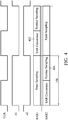
- FIG. 4 depicts a timing diagram for operating the ADC of FIG. 3 in accordance with an exemplary embodiment of the disclosure.
- the SAR blocks SAR1 and SAR2 each uses a full input sampling cycle (1/fs) to sample the input voltage Vin.
- the SAR block SAR1 samples the input voltage Vin
- the SAR block SAR2 performs successive approximation and holds the residue voltage Vres2 for the noise-shaping circuit 202 to sample.
- a half input sampling cycle of SAR conversion is followed by another half input sampling cycle of residue sampling.
- the SAR block SAR1 When the input voltage Vin is switched to be sampled by the SAR block SAR2, the SAR block SAR1 is switched to perform the successive approximation and holds the residue voltage Vres1 for the noise-shaping circuit 202 to sample.
- the residue voltage Vres1/Vres2 is transformed to the noise-shaping signal Sns by the noise-shaping circuit 202.
- the residue voltage Vres1/Vres2 obtained in the earlier residue sampling (e.g., the residue voltage Vres2 obtained in the residue sampling 404) may be taken into consideration, depending on the delay provided by the loop filter 204.
- the ADC of FIG. 3 containing more than one SAR block and operated according to the timing diagram of FIG. 4 achieves a higher sampling rate fs.
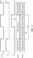
- FIG. 5 depicts a timing diagram for operating the ADC of FIG. 3 in accordance with another exemplary embodiment of the disclosure.
- the SAR blocks SAR1 and SAR2 each use only a half input sampling cycle (1/2fs) to sample the input voltage Vin.
- the SAR block SAR1 samples the input voltage Vin when the SAR block SAR2 is still in the SAR conversion process.
- the SAR block SAR2 also ends the SAR conversion.
- the SAR block SAR1 starts the SAR conversion that lasts a full input sample cycle (1/fs) and the noise-shaping circuit 202 starts sampling the residue voltage Vres2 that lasts a half input sampling cycle.
- the SAR block SAR2 After the residue sampling, the SAR block SAR2 performs the next sampling process of the input voltage Vin and meanwhile the SAR block SAR1 continues the SAR conversion.
- the SAR conversion of the SAR block SAR1 ends with the input sampling process of the SAR block SAR2.
- the noise-shaping circuit 202 is switched to sample the residue voltage Vres1 and the SAR block SAR2 is switched to do successive approximation.
- the residue voltage Vres1/Vres2 is transformed to the noise-shaping signal Sns by the noise-shaping circuit 202.
- the residue voltage Vres1/Vres2 obtained in the earlier residue sampling may be taken into consideration, depending on the delay provided by the loop filter 204.
- the residue voltage Vres2 obtained in interval 502 may be used later in the SAR conversion 504.
- the ADC of FIG. 3 containing more than one SAR block and operated according to the timing diagram of FIG. 5 achieves a higher sampling rate fs.
- more than two SAR blocks may be used in other exemplary embodiments of the disclosure for a higher-order interleaving architecture.
- the input voltage Vin is sampled by the different SAR blocks alternately to guarantee a high sampling rate. For each SAR block, there is sufficient time to perform SAR conversion and residue sampling while the other SAR blocks take turns in sampling the input voltage Vin.
- the control of the SAR ADC of the disclosure is organized as follows.
- the input sampling interval of the first SAR block SAR1 overlaps the residue sampling interval of the second SAR block SAR2.
- the residue sampling interval of the second SAR block SAR2 and the input sampling interval of the first SAR block SAR1 may end together.
- the input sampling interval of the first SAR block SAR1 may last a full input sampling cycle 1/fs.
- the input sampling interval of the second SAR block SAR2 repeated after the residue sampling interval of the second SAR block SAR2 and following the input sampling interval of the first SAR block SAR1 may also last a full input sampling cycle 1/fs.
- the SAR conversion interval of the first SAR block SAR1 may start with the input sampling interval of the second SAR block SAR2.
- the residue sampling interval of the first SAR block SAR1 may overlap the input sampling interval of the second SAR block SAR2.
- the residue sampling interval of the first SAR block SAR1 and the input sampling interval of the second SAR block SAR2 may end together.
- the SAR interval and the residue sampling interval of the first SAR block SAR1 each may last a half input sampling cycle 1/2fs.
- the input sampling interval of the first SAR block SAR1 may further overlap the SAR conversion interval of the second SAR block SAR2.
- the SAR conversion interval of the second SAR block SAR2 and the input sampling interval of the first SAR block SAR1 may start together.
- the SAR interval and the residue sampling interval of the second SAR block SAR2 each may last a half input sampling cycle 1/2fs.
- the control scheme depicted in FIG. 4 is one example of these exemplary control schemes.
- the input sampling interval of the first SAR block SAR1 overlaps a SAR conversion interval of the second SAR block SAR2.
- the input sampling interval of the first SAR block SAR1 and the SAR conversion interval of the second SAR block SAR2 may end together.
- the residue sampling interval plus the input sampling interval may equal a full input sampling cycle 1/fs and may be allocated within the SAR conversion interval of the first SAR block SAR1.
- the SAR interval of the first SAR block SAR1 lasts a full input sampling cycle 1/fs.
- the input sampling interval and the residue sampling interval of the first SAR block SAR1 each may last a half input sampling cycle 1/2fs.
- the input sampling interval and the residue sampling interval of the second SAR block SAR2 each may last a half input sampling cycle 1/2fs.
- the control scheme depicted in FIG. 5 is one example of these exemplary control schemes.
Landscapes
- Engineering & Computer Science (AREA)
- Theoretical Computer Science (AREA)
- Analogue/Digital Conversion (AREA)
Abstract
Description
- The present invention relates to analog-to-digital converters (ADCs).
- In electronics, an analog-to-digital converter is a system that converts an analog input into a digital signal. ADCs with charge-redistribution successive approximation (SAR) are common today.
-
FIG. 1 depicts an example of a successive approximation analog-to-digital converter (SAR ADC). During the first operation phase, an input voltage Vin is bottom-plate sampled onto aweighted capacitor array 102. After this sampling phase, the bottom plates of the capacitors within theweighted capacitor array 102 are switched to a common-mode voltage GND for a successive approximation scheme. Thecomparator 104 tests the sign of the sampled voltage (obtained from the top plate TP of the weighted capacitor array 102) and the sign decision output from thecomparator 104 is fed back to switch the bottom plate voltage of the current MSB (Most Significant Bit) capacitor within theweighted capacitor array 102. When a voltage subtraction is required, the bottom plate of the current MSB capacitor is switched to the lower reference voltage Vrefl. When a voltage addition is required, the bottom plate of the current MSB capacitor is switched to the higher reference voltage Vrefh. The bottom plates of the capacitors within theweighted capacitor array 102 are switched one by one in the successive approximation scheme. The output of thecomparator 104 is collected and transformed to a digital representation Dout of the input voltage Vin. - However, the sampling phase plus the successive approximation scheme limit the speed of the analog-to-digital conversion.
- Furthermore, quantization error and noise from the
comparator 104 should also be taken into consideration when designing an analog-to-digital converter. - An interleaving successive approximation analog-to-digital converter (SAR ADC) with noise-shaping is shown.
- An interleaving SAR ADC with noise shaping in accordance with an exemplary embodiment of the disclosure has a first SAR block, a second SAR block, and a noise-shaping circuit. The first and second SAR blocks take turns to sample an input voltage for successive approximation of the input voltage and observation of a digital representation of the input voltage. The noise-shaping circuit receives a first residue voltage from the first SAR block and receives a second residue voltage from the second SAR block alternately, and outputs a noise-shaping signal to be fed into the first SAR block and the second SAR block.
- A detailed description is given in the following embodiments with reference to the accompanying drawings.
- The present invention can be more fully understood by reading the subsequent detailed description and examples with references made to the accompanying drawings, wherein:
-
FIG. 1 depicts an example of a SAR ADC; -
FIG. 2 depicts a SAR ADC with noise shaping; -
FIG. 3 depicts an interleaving SAR ADC with noise shaping in accordance with an exemplary embodiment of the disclosure; -
FIG. 4 depicts a timing diagram for operating the ADC ofFIG. 3 in accordance with an exemplary embodiment of the disclosure; and -
FIG. 5 depicts a timing diagram for operating the ADC ofFIG. 3 in accordance with another exemplary embodiment of the disclosure. - The following description shows exemplary embodiments carrying out the invention. This description is made for the purpose of illustrating the general principles of the invention and should not be taken in a limiting sense. The scope of the invention is best determined by reference to the appended claims.
- Referring to the SAR ADC of
FIG. 1 , the top plate TP of theweighted capacitor array 102 is coupled to thecomparator 104 for trials of successive approximation (by which thecomparator 104 outputs a series of comparison result to switch theweighted capacitor array 102 to successive approximate the value of the input voltage Vin). In the disclosure, a residue voltage (Vres hereinafter) of successive approximation (e.g., a voltage value retrieved from the top plate TP of the weighted capacitor array 102) is further used to develop a noise shaping technique. A noise-shaping signal (Sns hereinafter) is generated from the residue voltage Vres and fed to the negative input of thecomparator 104 and thereby quantization noise and comparator noise of a SAR ADC are attenuated. -
FIG. 2 depicts a SAR ADC with noise shaping. In the upper illustration ofFIG. 2 , a functional representation of a SAR ADC with noise shaping is shown. In addition to the basic SAR architecture including theweighted capacitor array 102 and thecomparator 104 described inFIG. 1 , the upper illustration further illustrates a noise-shaping circuit 202 which is operative to transform the residue voltage Vres output by theweighted capacitor array 102 to provide the negative input of thecomparator 104 with the noise-shaping signal Sns. For an N-bit analog-to-digital conversion, the residue voltage Vres may be obtained from the top plate TP of theweighted capacitor array 102 after the Nth decision is made by thecomparator 104. The residue voltage Vres, therefore, contains the noise information. After being processed by the noise-shapingcircuit 202, the residue voltage Vres is transformed to the noise-shaping signal Sns to shape the noise in the succeeding analog-to-digital conversion(s). In the lower illustration ofFIG. 2 , an equivalent signal flow diagram is shown. The noise-shaping circuit 202 introduces aloop filter 204 in the z transfer function of the SAR ADC. The quantization noise Q or even the comparator noise (not shown in the figure) can be reduced by the noise-shaping technique. - The noise-
shaping circuit 202 may simply include a battery capacitor that is charge-shared with the top plate TP of theweighted capacitor array 102. In some examples, the noise-shaping circuit 202 may further include an integrator coupled to the battery capacitor. In other examples, the noise-shapingcircuit 202 includes cascaded circuits which form a cascaded FIR-IIR loop filter. Any circuit that imitates the noise within the analog-to-digital converter may be used as the noise-shapingcircuit 202. - To achieve a higher conversion rate, a concept of time interleaving is introduced here.
-
FIG. 3 depicts an interleaving SAR ADC with noise shaping in accordance with an exemplary embodiment of the disclosure. Based on the basic SAR architecture used with the noise shaping circuit 202 (referring back toFIG. 2 ), a SAR block SAR1 and another SAR block SAR2 are provided inFIG. 3 . The SAR block SAR1 and the SAR block SAR2 are switched (by the control signals φ1 and φ2) to sample the input voltage Vin in an interleaving way. When one of the SAR blocks SAR1 or SAR2 is sampling the input voltage Vin, the other is performing successive approximation or even residue sampling. A higher net sample rate is achieved. As shown, the noise-shaping circuit 202 is shared by the two SAR blocks SAR1 or SAR2. The residue voltages Vres1 and Vres2 from the SAR blocks SAR1 and SAR2 are sampled into the noise-shapingcircuit 202 alternately. Therefore, the noise-shaping signal Sns generated by the noise-shapingcircuit 202 based on the interleaving residue voltages Vres1 and Vres2 includes sufficient noise information. The noise-shaping signal Sns is coupled to both of the SAR blocks SAR1 and SAR2. The successive approximation performed in the SAR blocks SAR1 and SAR2 is considerably improved. The digital representation Dout1 obtained by the SAR block SAR1 and the digital representation Dout2 obtained by the SAR block SAR2 are output by the multiplexer Mux as Dout. A changed input voltage Vin can be converted to a digital form and represented by the digital representation Dout. -
FIG. 4 depicts a timing diagram for operating the ADC ofFIG. 3 in accordance with an exemplary embodiment of the disclosure. Referring to the control signals φ1 and φ2, the SAR blocks SAR1 and SAR2 each uses a full input sampling cycle (1/fs) to sample the input voltage Vin. The bandwidth requirement of the front-end buffer preceding the ADC, therefore, is relaxed. When the SAR block SAR1 samples the input voltage Vin, the SAR block SAR2 performs successive approximation and holds the residue voltage Vres2 for the noise-shaping circuit 202 to sample. As shown, a half input sampling cycle of SAR conversion is followed by another half input sampling cycle of residue sampling. When the input voltage Vin is switched to be sampled by the SAR block SAR2, the SAR block SAR1 is switched to perform the successive approximation and holds the residue voltage Vres1 for the noise-shaping circuit 202 to sample. The residue voltage Vres1/Vres2 is transformed to the noise-shaping signal Sns by the noise-shaping circuit 202. When theSAR conversion 402 is performed, the residue voltage Vres1/Vres2 obtained in the earlier residue sampling (e.g., the residue voltage Vres2 obtained in the residue sampling 404) may be taken into consideration, depending on the delay provided by theloop filter 204. In comparison with the SAR ADC ofFIG. 2 that uses only a single SAR block, the ADC ofFIG. 3 containing more than one SAR block and operated according to the timing diagram ofFIG. 4 achieves a higher sampling rate fs. -
FIG. 5 depicts a timing diagram for operating the ADC ofFIG. 3 in accordance with another exemplary embodiment of the disclosure. Referring to the control signals φ1 and φ2, the SAR blocks SAR1 and SAR2 each use only a half input sampling cycle (1/2fs) to sample the input voltage Vin. The SAR block SAR1 samples the input voltage Vin when the SAR block SAR2 is still in the SAR conversion process. When the SAR block SAR1 ends the input sampling, the SAR block SAR2 also ends the SAR conversion. Then, the SAR block SAR1 starts the SAR conversion that lasts a full input sample cycle (1/fs) and the noise-shaping circuit 202 starts sampling the residue voltage Vres2 that lasts a half input sampling cycle. After the residue sampling, the SAR block SAR2 performs the next sampling process of the input voltage Vin and meanwhile the SAR block SAR1 continues the SAR conversion. The SAR conversion of the SAR block SAR1 ends with the input sampling process of the SAR block SAR2. Then, the noise-shaping circuit 202 is switched to sample the residue voltage Vres1 and the SAR block SAR2 is switched to do successive approximation. The residue voltage Vres1/Vres2 is transformed to the noise-shaping signal Sns by the noise-shaping circuit 202. When the SAR conversion is performed, the residue voltage Vres1/Vres2 obtained in the earlier residue sampling may be taken into consideration, depending on the delay provided by theloop filter 204. For example, the residue voltage Vres2 obtained ininterval 502 may be used later in theSAR conversion 504. In comparison with the SAR ADC ofFIG. 2 that uses only a single SAR block, the ADC ofFIG. 3 containing more than one SAR block and operated according to the timing diagram ofFIG. 5 achieves a higher sampling rate fs. - In addition to the two-way interleaving architecture described in
FIG. 3 , more than two SAR blocks may be used in other exemplary embodiments of the disclosure for a higher-order interleaving architecture. The input voltage Vin is sampled by the different SAR blocks alternately to guarantee a high sampling rate. For each SAR block, there is sufficient time to perform SAR conversion and residue sampling while the other SAR blocks take turns in sampling the input voltage Vin. - The control of the SAR ADC of the disclosure is organized as follows.
- In some exemplary embodiments, the input sampling interval of the first SAR block SAR1 overlaps the residue sampling interval of the second SAR block SAR2. The residue sampling interval of the second SAR block SAR2 and the input sampling interval of the first SAR block SAR1 may end together. The input sampling interval of the first SAR block SAR1 may last a full
input sampling cycle 1/fs. The input sampling interval of the second SAR block SAR2 repeated after the residue sampling interval of the second SAR block SAR2 and following the input sampling interval of the first SAR block SAR1 may also last a fullinput sampling cycle 1/fs. The SAR conversion interval of the first SAR block SAR1 may start with the input sampling interval of the second SAR block SAR2. The residue sampling interval of the first SAR block SAR1 may overlap the input sampling interval of the second SAR block SAR2. The residue sampling interval of the first SAR block SAR1 and the input sampling interval of the second SAR block SAR2 may end together. The SAR interval and the residue sampling interval of the first SAR block SAR1 each may last a halfinput sampling cycle 1/2fs. The input sampling interval of the first SAR block SAR1 may further overlap the SAR conversion interval of the second SAR block SAR2. The SAR conversion interval of the second SAR block SAR2 and the input sampling interval of the first SAR block SAR1 may start together. The SAR interval and the residue sampling interval of the second SAR block SAR2 each may last a halfinput sampling cycle 1/2fs. The control scheme depicted inFIG. 4 is one example of these exemplary control schemes. - In some exemplary embodiments, the input sampling interval of the first SAR block SAR1 overlaps a SAR conversion interval of the second SAR block SAR2. The input sampling interval of the first SAR block SAR1 and the SAR conversion interval of the second SAR block SAR2 may end together. For the second SAR block SAR2, the residue sampling interval plus the input sampling interval may equal a full
input sampling cycle 1/fs and may be allocated within the SAR conversion interval of the first SAR block SAR1. The SAR interval of the first SAR block SAR1 lasts a fullinput sampling cycle 1/fs. The input sampling interval and the residue sampling interval of the first SAR block SAR1 each may last a halfinput sampling cycle 1/2fs. The input sampling interval and the residue sampling interval of the second SAR block SAR2 each may last a halfinput sampling cycle 1/2fs. The control scheme depicted inFIG. 5 is one example of these exemplary control schemes. - While the invention has been described by way of example and in terms of the preferred embodiments, it should be understood that the invention is not limited to the disclosed embodiments. On the contrary, it is intended to cover various modifications and similar arrangements (as would be apparent to those skilled in the art). Therefore, the scope of the appended claims should be accorded the broadest interpretation so as to encompass all such modifications and similar arrangements.
Claims (15)
- An interleaving successive approximation analog-to-digital converter (FIG. 3) with noise shaping, comprising:a first successive approximation block (SAR1) and a second successive approximation block (SAR2), taking turns to sample an input voltage (Vin) for successive approximation of the input voltage and observation of a digital representation (Dout) of the input voltage; anda noise-shaping circuit (202), receiving a first residue voltage (Vres1) from the first successive approximation block and receiving a second residue voltage (Vres2) from the second successive approximation block alternately, and outputting a noise-shaping signal (Sns) to be fed into the first successive approximation block and the second successive approximation block.
- The interleaving successive approximation analog-to-digital converter with noise shaping as claimed in claim 1, wherein:an input sampling interval of the first successive approximation block overlaps a residue sampling interval of the second successive approximation block;the residue sampling interval of the second successive approximation block follows a successive approximation conversion interval of the second successive approximation block;during the input sampling interval of the first successive approximation block, the first successive approximation block samples the input voltage;during the successive approximation conversion interval of the second successive approximation block, the second successive approximation block performs successive approximation of the input voltage; andduring the residue sampling interval of the second successive approximation block, the second successive approximation block holds the second residue voltage for the noise-shaping circuit to sample.
- The interleaving successive approximation analog-to-digital converter with noise shaping as claimed in claim 2, wherein:the input sampling interval of the first successive approximation block lasts a full input sampling cycle.
- The interleaving successive approximation analog-to-digital converter with noise shaping as claimed in claim 3, wherein:an input sampling interval of the second successive approximation block is repeated after the residue sampling interval of the second successive approximation block;during the input sampling interval of the second successive approximation block, the second successive approximation block samples the input voltage;the input sampling interval of the second successive approximation block follows and the input sampling interval of the first successive approximation block; andthe input sampling interval of the second successive approximation block lasts a full input sampling cycle.
- The interleaving successive approximation analog-to-digital converter with noise shaping as claimed in claim 4, wherein:a successive approximation conversion interval of the first successive approximation block starts with the input sampling interval of the second successive approximation block; andduring the successive approximation conversion interval of the first successive approximation block, the first successive approximation block performs successive approximation of the input voltage.
- The interleaving successive approximation analog-to-digital converter with noise shaping as claimed in claim 5, wherein:a residue sampling interval of the first successive approximation block follows the successive approximation conversion interval of the first successive approximation block;during the residue sampling interval of the first successive approximation block, the noise-shaping circuit samples the first residue voltage of first successive approximation block; andthe residue sampling interval of the first successive approximation block overlaps the input sampling interval of the second successive approximation block.
- The interleaving successive approximation analog-to-digital converter with noise shaping as claimed in claim 6, wherein:the successive approximation conversion interval of the first successive approximation block lasts a half input sampling cycle; andthe residue sampling interval of the first successive approximation block lasts a half input sampling cycle.
- The interleaving successive approximation analog-to-digital converter with noise shaping as claimed in claim 7, wherein:the input sampling interval of the first successive approximation block further overlaps the successive approximation conversion interval of the second successive approximation block.
- The interleaving successive approximation analog-to-digital converter with noise shaping as claimed in claim 8, wherein:the successive approximation conversion interval of the second successive approximation block lasts a half input sampling cycle; andthe residue sampling interval of the second successive approximation block lasts a half input sampling cycle.
- The interleaving successive approximation analog-to-digital converter with noise shaping as claimed in claim 1, wherein:an input sampling interval of the first successive approximation block overlaps a successive approximation conversion interval of the second successive approximation block;during the input sampling interval of the first successive approximation block, the first successive approximation block samples the input voltage;during the successive approximation conversion interval of the second successive approximation block, the second successive approximation block performs successive approximation of the input voltage.
- The interleaving successive approximation analog-to-digital converter with noise shaping as claimed in claim 10, wherein:a residue sampling interval of the second successive approximation block follows the successive approximation conversion interval of the second successive approximation block;during the residue sampling interval of the second successive approximation block, the noise-shaping circuit samples the second residue voltage of second successive approximation block;an input sampling interval of the second successive approximation block is repeated after the residue sampling interval of the second successive approximation block;during the input sampling interval of the second successive approximation block, the second successive approximation block samples the input voltage; andthe residue sampling interval of the second successive approximation block plus the input sampling interval of the second successive approximation block equals a full input sampling cycle.
- The interleaving successive approximation analog-to-digital converter with noise shaping as claimed in claim 11, wherein:a successive approximation conversion interval of the first successive approximation block follows the input sampling interval of the first successive approximation block;during the successive approximation conversion interval of the first successive approximation block, the first successive approximation block performs successive approximation of the input voltage; andthe residue sampling interval of the second successive approximation block and the input sampling interval of the second successive approximation block are within the successive approximation conversion interval of the first successive approximation block.
- The interleaving successive approximation analog-to-digital converter with noise shaping as claimed in claim 12, wherein:the successive approximation conversion interval of the first successive approximation block lasts a full input sampling cycle.
- The interleaving successive approximation analog-to-digital converter with noise shaping as claimed in claim 13, wherein:a residue sampling interval of the first successive approximation block follows the successive approximation conversion interval of the first successive approximation block; andduring the residue sampling interval of the first successive approximation block, the noise-shaping circuit samples the first residue voltage of first successive approximation block.
- The interleaving successive approximation analog-to-digital converter with noise shaping as claimed in claim 14, wherein:the input sampling interval of the first successive approximation block lasts a half input sampling cycle;the residue sampling interval of the first successive approximation block lasts a half input sampling cycle;the residue sampling interval of the second successive approximation block lasts a half input sampling cycle; andthe input sampling interval of the second successive approximation block lasts a half input sampling cycle.
Applications Claiming Priority (2)
| Application Number | Priority Date | Filing Date | Title |
|---|---|---|---|
| US201662439196P | 2016-12-27 | 2016-12-27 | |
| US15/830,327 US10110242B2 (en) | 2016-12-27 | 2017-12-04 | Interleaving successive approximation analog-to-digital converter with noise shaping |
Publications (1)
| Publication Number | Publication Date |
|---|---|
| EP3343775A1 true EP3343775A1 (en) | 2018-07-04 |
Family
ID=60702423
Family Applications (1)
| Application Number | Title | Priority Date | Filing Date |
|---|---|---|---|
| EP17209103.5A Ceased EP3343775A1 (en) | 2016-12-27 | 2017-12-20 | Interleaving successive approximation analog-to-digital converter with noise shaping |
Country Status (4)
| Country | Link |
|---|---|
| US (1) | US10110242B2 (en) |
| EP (1) | EP3343775A1 (en) |
| CN (1) | CN108242927B (en) |
| TW (1) | TWI647917B (en) |
Families Citing this family (21)
| Publication number | Priority date | Publication date | Assignee | Title |
|---|---|---|---|---|
| US10284213B2 (en) * | 2017-04-21 | 2019-05-07 | Analog Devices, Inc. | Analog-to-digital converter reusing comparator for residue amplifier for noise shaping |
| US10312926B2 (en) | 2017-10-30 | 2019-06-04 | Analog Devices Global Unlimited Company | Noise-shaping analog-to-digital converter |
| DE102018126603B4 (en) | 2017-10-30 | 2023-01-12 | Analog Devices International Unlimited Company | Noise shaping analog to digital converter |
| CN109067398B (en) * | 2018-07-16 | 2022-04-01 | 珠海一微半导体股份有限公司 | Control method of ADC circuit with multi-channel signals |
| US10840932B2 (en) * | 2018-10-12 | 2020-11-17 | Mediatek Inc. | Analog-to-digital converter |
| US10763875B2 (en) * | 2019-01-11 | 2020-09-01 | Realtek Semiconductor Corporation | Switched capacitor circuit and analog-to-digital converter device |
| US10790843B2 (en) | 2019-01-11 | 2020-09-29 | Realtek Semiconductor Corporation | Analog-to-digital converter device |
| US10778242B2 (en) | 2019-01-11 | 2020-09-15 | Realtek Semiconductor Corporation | Analog-to-digital converter device |
| CN110113051B (en) * | 2019-05-13 | 2020-03-31 | 深圳锐越微技术有限公司 | Analog-to-digital converter error shaping circuit and successive approximation type analog-to-digital converter |
| CN110190854B (en) * | 2019-05-13 | 2023-05-12 | 东南大学 | A realization circuit and method for two-step SAR ADC sharing a set of reference voltages |
| CN112564704B (en) * | 2019-09-25 | 2023-04-07 | 深圳大学 | Successive approximation analog-to-digital converter with sampling time expansion function and electronic device |
| US11043958B2 (en) | 2019-10-22 | 2021-06-22 | Mediatek Inc. | Time-interleaved noise-shaping successive-approximation analog-to-digital converter |
| FR3105897B1 (en) | 2019-12-26 | 2023-10-27 | Thales Sa | Analog-to-digital conversion device comprising two cascaded analog-to-digital conversion stages with successive approximation register and noise shaping, and associated electronic sensor |
| CN111262586B (en) * | 2020-03-24 | 2022-03-29 | 电子科技大学 | Second-order noise shaping successive approximation analog-to-digital converter |
| US11658678B2 (en) | 2020-08-10 | 2023-05-23 | Analog Devices, Inc. | System and method to enhance noise performance in a delta sigma converter |
| CN112202449B (en) * | 2020-09-29 | 2023-04-07 | 华中科技大学 | Capacitance measuring circuit and measuring method based on analog-digital converter |
| TWI763228B (en) * | 2020-12-31 | 2022-05-01 | 瑞昱半導體股份有限公司 | Time-interleaved analog to digital converter having randomization and signal conversion method |
| CN112865798B (en) * | 2021-01-15 | 2024-05-07 | 中国科学院半导体研究所 | Noise shaping successive approximation analog-to-digital converter and noise shaping method |
| TWI748915B (en) * | 2021-04-15 | 2021-12-01 | 瑞昱半導體股份有限公司 | Analog to digital conversion apparatus and method having quick conversion mechanism |
| CN114389610A (en) * | 2021-12-30 | 2022-04-22 | 北京力通通信有限公司 | Analog-to-digital converter system |
| TWI819823B (en) * | 2022-09-29 | 2023-10-21 | 瑞昱半導體股份有限公司 | Time-interleaved analog to digital converter based on control of counter |
Citations (2)
| Publication number | Priority date | Publication date | Assignee | Title |
|---|---|---|---|---|
| US20160035235A1 (en) * | 2014-08-01 | 2016-02-04 | Forclass Ltd. | System and method thereof for enhancing students engagement and accountability |
| US20160352351A1 (en) * | 2015-05-27 | 2016-12-01 | Panasonic Intellectual Property Management Co., Ltd. | Ad converter including a capacitive dac |
Family Cites Families (11)
| Publication number | Priority date | Publication date | Assignee | Title |
|---|---|---|---|---|
| US7675452B2 (en) * | 2008-05-01 | 2010-03-09 | Analog Devices, Inc. | Successive approximation register analog to digital converter with improved immunity to time varying noise |
| WO2010044000A1 (en) * | 2008-10-13 | 2010-04-22 | Nxp B.V. | An adc |
| KR101122462B1 (en) * | 2009-11-02 | 2012-03-02 | 고려대학교 산학협력단 | Successive approxiamation analog/digtal converter and time-interleaved successive approxiamation analog/digtal converter |
| TWI446723B (en) * | 2011-03-08 | 2014-07-21 | Univ Macau | Analog to digital converter circuit |
| TWI521887B (en) * | 2013-12-06 | 2016-02-11 | 碩頡科技股份有限公司 | Successive approximation register anolog-to-digital converter |
| US9191023B2 (en) * | 2014-02-05 | 2015-11-17 | Analog Devices Global | Analog to digital converter and a method of operating an analog to digital converter |
| KR101680081B1 (en) * | 2014-12-12 | 2016-11-29 | 서강대학교산학협력단 | 2nd-order noise-shaping Successive Approximation Register Analog to Digital Converter |
| US9294110B1 (en) * | 2015-01-29 | 2016-03-22 | Qualcomm Incorporated | Correction circuits for successive-approximation-register analog-to-digital converters |
| US9425818B1 (en) * | 2015-05-28 | 2016-08-23 | Qualcomm Incorporated | Noise shaping successive approximation register analog-to-digital converter |
| US9722746B2 (en) * | 2015-09-22 | 2017-08-01 | Mediatek Inc. | Analog-to-digital converter with bandpass noise transfer function |
| US9455737B1 (en) * | 2015-09-25 | 2016-09-27 | Qualcomm Incorporated | Delta-sigma analog-to-digital converter (ADC) with time-interleaved (TI) or two-step successive approximation register (SAR) quantizer |
-
2017
- 2017-12-04 US US15/830,327 patent/US10110242B2/en active Active
- 2017-12-12 CN CN201711322130.7A patent/CN108242927B/en active Active
- 2017-12-13 TW TW106143711A patent/TWI647917B/en not_active IP Right Cessation
- 2017-12-20 EP EP17209103.5A patent/EP3343775A1/en not_active Ceased
Patent Citations (2)
| Publication number | Priority date | Publication date | Assignee | Title |
|---|---|---|---|---|
| US20160035235A1 (en) * | 2014-08-01 | 2016-02-04 | Forclass Ltd. | System and method thereof for enhancing students engagement and accountability |
| US20160352351A1 (en) * | 2015-05-27 | 2016-12-01 | Panasonic Intellectual Property Management Co., Ltd. | Ad converter including a capacitive dac |
Non-Patent Citations (3)
| Title |
|---|
| JEFFREY ALAN FREDENBURG: "Noise-Shaping SAR ADCs", 1 January 2015 (2015-01-01), XP055470990, Retrieved from the Internet <URL:https://deepblue.lib.umich.edu/bitstream/handle/2027.42/113647/fredenbu_1.pdf?sequence=1&isAllowed=y> [retrieved on 20180426] * |
| MENG XIN ET AL: "A noise-coupled time-interleaved delta-sigma modulator with shifted loop delays", 2015 IEEE INTERNATIONAL SYMPOSIUM ON CIRCUITS AND SYSTEMS (ISCAS), IEEE, 24 May 2015 (2015-05-24), pages 2045 - 2048, XP033183564, DOI: 10.1109/ISCAS.2015.7169079 * |
| WATERS ALLEN ET AL: "Highly time-interleaved noise-shaped SAR ADC with reconfigurable order", 2016 IEEE INTERNATIONAL SYMPOSIUM ON CIRCUITS AND SYSTEMS (ISCAS), IEEE, 22 May 2016 (2016-05-22), pages 1026 - 1029, XP032941727, DOI: 10.1109/ISCAS.2016.7527418 * |
Also Published As
| Publication number | Publication date |
|---|---|
| TWI647917B (en) | 2019-01-11 |
| TW201840136A (en) | 2018-11-01 |
| US20180183450A1 (en) | 2018-06-28 |
| CN108242927A (en) | 2018-07-03 |
| US10110242B2 (en) | 2018-10-23 |
| CN108242927B (en) | 2021-06-29 |
Similar Documents
| Publication | Publication Date | Title |
|---|---|---|
| US10110242B2 (en) | Interleaving successive approximation analog-to-digital converter with noise shaping | |
| KR102103933B1 (en) | Successive approximation analog to digital converter and method of analog to digital conversion | |
| US7551114B2 (en) | Reducing power consumption in the early stages of a pipeline sub-ADC used in a time-interleaved ADC | |
| US8643529B2 (en) | SAR assisted pipelined ADC and method for operating the same | |
| JP6353267B2 (en) | AD converter and AD conversion method | |
| EP2055006B1 (en) | Analog-to-digital conversion using asynchronous current-mode cyclic comparison | |
| EP2924880A1 (en) | Multiplying digital-to-analog converter and pipeline analog-to-digital converter using the same | |
| US9432046B1 (en) | Successive approximation analog-to-digital converter | |
| US8362939B2 (en) | Switched-capacitor pipeline ADC stage | |
| JP2010193089A (en) | Discrete time circuit | |
| US8018361B2 (en) | Area-efficient analog-to-digital converter | |
| CN111435835B (en) | Switched capacitor circuit and analog-to-digital conversion device | |
| US7102559B2 (en) | Analog-to-digital converter having interleaved coarse sections coupled to a single fine section | |
| EP3490152B1 (en) | Interleaving quantizer in continuous-time delta-sigma modulator for quantization level increment | |
| US7821436B2 (en) | System and method for reducing power dissipation in an analog to digital converter | |
| EP2811654B1 (en) | Resolution-boosted sigma delta analog-to-digital converter | |
| JP2016039418A (en) | A/d conversion circuit | |
| KR100884166B1 (en) | AD / DA conversion unit | |
| US20110122007A1 (en) | Semiconductor storage device and method of manufacturing thereof | |
| JP2011066619A (en) | Ad converter | |
| CN100576748C (en) | Analog-to-digital conversion device, analog-to-digital conversion method, and signal processing system using the conversion device | |
| EP3480949A1 (en) | Multiplying digital-to-analog conversion circuit | |
| CN114337672B (en) | Analog-to-digital converter and analog-to-digital conversion method | |
| CN207504850U (en) | Oversampling type Pipeline SAR-ADC device | |
| CN111295843B (en) | A pipelined analog-to-digital converter with at least three sampling channels |
Legal Events
| Date | Code | Title | Description |
|---|---|---|---|
| PUAI | Public reference made under article 153(3) epc to a published international application that has entered the european phase |
Free format text: ORIGINAL CODE: 0009012 |
|
| STAA | Information on the status of an ep patent application or granted ep patent |
Free format text: STATUS: THE APPLICATION HAS BEEN PUBLISHED |
|
| AK | Designated contracting states |
Kind code of ref document: A1 Designated state(s): AL AT BE BG CH CY CZ DE DK EE ES FI FR GB GR HR HU IE IS IT LI LT LU LV MC MK MT NL NO PL PT RO RS SE SI SK SM TR |
|
| AX | Request for extension of the european patent |
Extension state: BA ME |
|
| STAA | Information on the status of an ep patent application or granted ep patent |
Free format text: STATUS: REQUEST FOR EXAMINATION WAS MADE |
|
| 17P | Request for examination filed |
Effective date: 20181120 |
|
| RBV | Designated contracting states (corrected) |
Designated state(s): AL AT BE BG CH CY CZ DE DK EE ES FI FR GB GR HR HU IE IS IT LI LT LU LV MC MK MT NL NO PL PT RO RS SE SI SK SM TR |
|
| STAA | Information on the status of an ep patent application or granted ep patent |
Free format text: STATUS: EXAMINATION IS IN PROGRESS |
|
| 17Q | First examination report despatched |
Effective date: 20200227 |
|
| STAA | Information on the status of an ep patent application or granted ep patent |
Free format text: STATUS: THE APPLICATION HAS BEEN REFUSED |
|
| 18R | Application refused |
Effective date: 20220113 |