EP3343768B1 - Systems and methods for a gate drive circuit - Google Patents
Systems and methods for a gate drive circuit Download PDFInfo
- Publication number
- EP3343768B1 EP3343768B1 EP17207351.2A EP17207351A EP3343768B1 EP 3343768 B1 EP3343768 B1 EP 3343768B1 EP 17207351 A EP17207351 A EP 17207351A EP 3343768 B1 EP3343768 B1 EP 3343768B1
- Authority
- EP
- European Patent Office
- Prior art keywords
- shaping
- switch
- control switch
- control
- wbg
- Prior art date
- Legal status (The legal status is an assumption and is not a legal conclusion. Google has not performed a legal analysis and makes no representation as to the accuracy of the status listed.)
- Active
Links
Images


Classifications
-
- H—ELECTRICITY
- H03—ELECTRONIC CIRCUITRY
- H03K—PULSE TECHNIQUE
- H03K17/00—Electronic switching or gating, i.e. not by contact-making and –breaking
- H03K17/51—Electronic switching or gating, i.e. not by contact-making and –breaking characterised by the components used
-
- H—ELECTRICITY
- H03—ELECTRONIC CIRCUITRY
- H03K—PULSE TECHNIQUE
- H03K17/00—Electronic switching or gating, i.e. not by contact-making and –breaking
- H03K17/06—Modifications for ensuring a fully conducting state
- H03K17/063—Modifications for ensuring a fully conducting state in field-effect transistor switches
-
- H—ELECTRICITY
- H03—ELECTRONIC CIRCUITRY
- H03K—PULSE TECHNIQUE
- H03K17/00—Electronic switching or gating, i.e. not by contact-making and –breaking
- H03K17/08—Modifications for protecting switching circuit against overcurrent or overvoltage
- H03K17/081—Modifications for protecting switching circuit against overcurrent or overvoltage without feedback from the output circuit to the control circuit
- H03K17/0812—Modifications for protecting switching circuit against overcurrent or overvoltage without feedback from the output circuit to the control circuit by measures taken in the control circuit
- H03K17/08122—Modifications for protecting switching circuit against overcurrent or overvoltage without feedback from the output circuit to the control circuit by measures taken in the control circuit in field-effect transistor switches
-
- H—ELECTRICITY
- H03—ELECTRONIC CIRCUITRY
- H03K—PULSE TECHNIQUE
- H03K17/00—Electronic switching or gating, i.e. not by contact-making and –breaking
- H03K17/16—Modifications for eliminating interference voltages or currents
- H03K17/168—Modifications for eliminating interference voltages or currents in composite switches
-
- H—ELECTRICITY
- H03—ELECTRONIC CIRCUITRY
- H03K—PULSE TECHNIQUE
- H03K17/00—Electronic switching or gating, i.e. not by contact-making and –breaking
- H03K17/16—Modifications for eliminating interference voltages or currents
- H03K17/161—Modifications for eliminating interference voltages or currents in field-effect transistor switches
- H03K17/162—Modifications for eliminating interference voltages or currents in field-effect transistor switches without feedback from the output circuit to the control circuit
- H03K17/163—Soft switching
-
- H—ELECTRICITY
- H03—ELECTRONIC CIRCUITRY
- H03K—PULSE TECHNIQUE
- H03K17/00—Electronic switching or gating, i.e. not by contact-making and –breaking
- H03K17/51—Electronic switching or gating, i.e. not by contact-making and –breaking characterised by the components used
- H03K17/56—Electronic switching or gating, i.e. not by contact-making and –breaking characterised by the components used by the use, as active elements, of semiconductor devices
- H03K17/567—Circuits characterised by the use of more than one type of semiconductor device, e.g. BIMOS, composite devices such as IGBT
-
- H—ELECTRICITY
- H03—ELECTRONIC CIRCUITRY
- H03K—PULSE TECHNIQUE
- H03K17/00—Electronic switching or gating, i.e. not by contact-making and –breaking
- H03K17/08—Modifications for protecting switching circuit against overcurrent or overvoltage
- H03K17/081—Modifications for protecting switching circuit against overcurrent or overvoltage without feedback from the output circuit to the control circuit
- H03K17/0812—Modifications for protecting switching circuit against overcurrent or overvoltage without feedback from the output circuit to the control circuit by measures taken in the control circuit
- H03K17/08128—Modifications for protecting switching circuit against overcurrent or overvoltage without feedback from the output circuit to the control circuit by measures taken in the control circuit in composite switches
-
- H—ELECTRICITY
- H10—SEMICONDUCTOR DEVICES; ELECTRIC SOLID-STATE DEVICES NOT OTHERWISE PROVIDED FOR
- H10D—INORGANIC ELECTRIC SEMICONDUCTOR DEVICES
- H10D30/00—Field-effect transistors [FET]
- H10D30/40—FETs having zero-dimensional [0D], one-dimensional [1D] or two-dimensional [2D] charge carrier gas channels
- H10D30/47—FETs having zero-dimensional [0D], one-dimensional [1D] or two-dimensional [2D] charge carrier gas channels having two-dimensional [2D] charge carrier gas channels, e.g. nanoribbon FETs or high electron mobility transistors [HEMT]
-
- H—ELECTRICITY
- H10—SEMICONDUCTOR DEVICES; ELECTRIC SOLID-STATE DEVICES NOT OTHERWISE PROVIDED FOR
- H10D—INORGANIC ELECTRIC SEMICONDUCTOR DEVICES
- H10D62/00—Semiconductor bodies, or regions thereof, of devices having potential barriers
- H10D62/80—Semiconductor bodies, or regions thereof, of devices having potential barriers characterised by the materials
-
- H—ELECTRICITY
- H10—SEMICONDUCTOR DEVICES; ELECTRIC SOLID-STATE DEVICES NOT OTHERWISE PROVIDED FOR
- H10D—INORGANIC ELECTRIC SEMICONDUCTOR DEVICES
- H10D62/00—Semiconductor bodies, or regions thereof, of devices having potential barriers
- H10D62/80—Semiconductor bodies, or regions thereof, of devices having potential barriers characterised by the materials
- H10D62/83—Semiconductor bodies, or regions thereof, of devices having potential barriers characterised by the materials being Group IV materials, e.g. B-doped Si or undoped Ge
- H10D62/832—Semiconductor bodies, or regions thereof, of devices having potential barriers characterised by the materials being Group IV materials, e.g. B-doped Si or undoped Ge being Group IV materials comprising two or more elements, e.g. SiGe
- H10D62/8325—Silicon carbide
-
- H—ELECTRICITY
- H10—SEMICONDUCTOR DEVICES; ELECTRIC SOLID-STATE DEVICES NOT OTHERWISE PROVIDED FOR
- H10D—INORGANIC ELECTRIC SEMICONDUCTOR DEVICES
- H10D62/00—Semiconductor bodies, or regions thereof, of devices having potential barriers
- H10D62/80—Semiconductor bodies, or regions thereof, of devices having potential barriers characterised by the materials
- H10D62/85—Semiconductor bodies, or regions thereof, of devices having potential barriers characterised by the materials being Group III-V materials, e.g. GaAs
- H10D62/8503—Nitride Group III-V materials, e.g. AlN or GaN
Definitions
- Embodiments of the subject matter described herein relate to a gate drive circuit for controlling operation of a wide bandgap semiconductor switch.
- Wide bandgap semiconductor switches may be utilized as electronic switches for power terminals of high voltage semiconductors operating at higher frequencies and temperatures relative to conventional semiconductors.
- the wide bandgap semiconductor switch has a low threshold voltage and high saturation velocity resulting in relatively quick transitions between ON and OFF states relative to conventional semiconductors.
- Conventional gate drive circuits only control activation and clamping of the wide bandgap semiconductor switch utilizing a secondary switch.
- JP 2013/026924 A describes a gate drive circuit capable of stably turning on a wide bandgap switching element without causing power fluctuation and without changing a switching characteristic at turn-on.
- the conventional gate drive circuits do not control a rate of rise of the gate, but simply activate the producing voltage spikes and/or oscillations (e.g., ringing). Thereby, there is a need for a gate drive circuit to operate the wide band gap semiconductor switch through a Miller plateau region.
- a system e.g., a gate drive system
- the system includes a wide bandgap switch (WBG switch) and a control switch conductively coupled to a control terminal and a gate terminal of the WBG switch.
- the WBG switch and the control switch are configured to have a common threshold voltage.
- the system further includes first and second shaping circuits conductively coupled to the control switch and the gate terminal of the WBG switch.
- the first and second shaping circuits and the control switch are configured to define an operation signal.
- the operation signal being configured to activate the WBG switch.
- the operation signal includes a profile based on electrical characteristics of the first and second shaping circuits.
- the method includes receiving a control signal and configuring an operation signal configured to activate a wide bandgap switch (WBG switch).
- WBG switch wide bandgap switch
- a profile of the operation signal being based on electrical characteristics of first and second shaping circuits.
- the method further includes delivering the operation signal to the WBG switch.
- a system e.g., a gate drive system
- the system includes a wide bandgap switch (WBG switch) and a control switch conductively coupled to a control terminal and a gate terminal of the WBG switch.
- the WBG switch and the control switch are configured to have a common activation threshold.
- the control switch having a gate terminal conductively coupled to a voltage source.
- the voltage source being a diode, a capacitor, or a control signal.
- the system further includes first and second shaping circuits conductively coupled to the control switch and the gate terminal of the WBG switch.
- the first and second shaping circuits and the control switch are configured to define an operation signal.
- the operation signal being formed by three shaping phases.
- a first shaping phase is defined by the electrical characteristics of the first and second shaping circuits.
- a second shaping phase is defined by the electrical characteristics of the second shaping circuit and the control switch.
- a third shaping phase is defined by the control switch.
- the operation signal is configured to activate the WBG switch.
- a profile of the operation signal being based on electrical characteristics of the first and second shaping circuits.
- a module, unit, or system may include a hardware and/or software system that operates to perform one or more functions.
- a module, unit, or system may include a computer processor, controller, or other logic-based device that performs operations based on instructions stored on a tangible and non-transitory computer readable storage medium, such as a computer memory.
- a module, unit, or system may include a hard-wired device that performs operations based on hard-wired logic of the device.
- the modules or units shown in the attached figures may represent the hardware that operates based on software or hardwired instructions, the software that directs hardware to perform the operations, or a combination thereof.
- the hardware may include electronic circuits that include and/or are connected to one or more logic-based devices, such as microprocessors, processors, controllers, or the like. These devices may be off-the-shelf devices that are appropriately programmed or instructed to perform operations described herein from the instructions described above. Additionally or alternatively, one or more of these devices may be hard-wired with logic circuits to perform these operations.
- logic-based devices such as microprocessors, processors, controllers, or the like.
- various embodiments provide methods and systems for a gate drive system having a gate drive circuit to operate a wide bandgap switch (WBG switch).
- the WBG switch may include Silicon Carbide (SiC), Aluminum Gallium Nitride (AlGaN), Gallium Nitride (GaN), Gallium Oxide (GaO), and/or the like.
- the gate drive circuit is configured to generate an operation signal configured to activate the WBG switch.
- the profile of the operation signal is based on electrical characteristics of the gate drive circuit. For example, the gate drive circuit controls a rate of rise and/or slope (e.g., amplitude) of the operation signal.
- the profile of the operation signal is configured to sustain the WBG switch operation within the Miller plateau region.
- the profile of the operation signal may be divided into three different shaping phases. For example, during the first shaping phase a gate voltage of the WBG switch is above the threshold activating the WBG switch, during the second shaping phase the gate voltage is configured to be sustained to operate the WBG switch within the Miller plateau region, and during the third shaping phase the gate voltage is clamped.
- At least one technical effect of various embodiments provides effective control of a drain voltage spike of the WBG switch. At least one technical effect of various embodiments provides low cost, easily implemented gate drive control circuit that enables control over the activation of the WBG switch without sacrificing deactivation of the WBG switch.
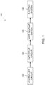
- FIG. 1 illustrates a block diagram of an embodiment of a gate drive system 100.
- the gate drive system 100 includes a controller circuit 102 and a wide bandgap switch 106 (WBG switch).
- the controller circuit 102 is configured to control the operation (e.g., activate, deactivate) of the WBG switch 106.
- the switch 106 may represent a high electron mobility transistor (HEMT).
- the WBG switch 106 may include SiC, AlGaN, GaN, GaO, and/or the like.
- the WBG switch 106 may be configured to control an electrical system 108.
- the electrical system 108 may represent an electric power system for a variable frequency drive, a drive train, a home appliance, and/or the like.
- the WBG switch 106 may be configured to switch between an ON state (e.g., saturation state) and an OFF state at a static and/or variable frequency (e.g., 100 kHz, 2 MHz, and/or the like) based on control signals received by the controller circuit 102.
- an ON state e.g., saturation state
- a static and/or variable frequency e.g., 100 kHz, 2 MHz, and/or the like
- the controller circuit 102 may be embodied in hardware, such as one or more processors, controller, or other logic-based device, that performs functions or operations based on one or more sets of instructions (e.g., software). Additionally or alternatively, the controller circuit 102 may be an application specific integrated circuit, a field programmable gate array, and/or the like configured to control the electrical system 108 via a gate drive circuit 104.
- the instructions on which the hardware operates may be stored on a tangible and non-transitory (e.g., not a transient signal) computer readable storage medium, such as memory.
- the memory may include one or more computer hard drives, flash drives, RAM, ROM, EEPROM and/or the like. Alternatively, one or more of the sets of instructions that direct operations of the hardware may be hard-wired into the logic of the hardware.
- the controller circuit 102 is configured to control the electrical system 108 based on control signals transmitted and/or communicated to the gate drive circuit 104.
- the gate drive circuit 104 may include a control switch 202 and a first and second shaping circuits 204, 206.
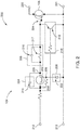
- FIG. 2 illustrates a schematic illustration 200 of an embodiment of the gate drive circuit 104.
- the control switch 202 is conductively coupled to a control terminals 212, 213 and a gate terminal 224 of the WBG switch 106.
- the control switch 202 may be a wide bandgap semiconductor similar to and/or the same as the WBG switch 106.
- the control switch 202 may include SiC, AlGaN, GaN, GaO, and/or the like
- the control switch 202 and the WBG switch 106 have a common threshold voltage (e.g., activation voltage) and/or electrical characteristics.
- the WBG switch 106 and the control switch 202 may both represent a high electron mobility transistor (HEMT).
- HEMT high electron mobility transistor
- the control terminals 212, 213 are conductively coupled to the controller circuit 102.
- the controller circuit 102 may send, transmit and/or conduct a control signal along the control terminal 212.
- the control signal may represent a pulse and/or electrical signal having a set voltage and/or current configured to enable the gate drive circuit 104 to generate the operation signal for the WBG switch 106.
- a gate terminal 226 of the control switch 202 is conductively coupled to a voltage source 208.
- the voltage source 208 is configured to provide a voltage potential to the gate terminal 226 to activate the control switch 202.
- the voltage source 208 shown in Figure 2 is a Zener diode 222.
- the Zener diode 222 is conductive coupled to the control terminal 212 having a cathode of the Zener diode 222 directly coupled to the gate terminal 226.
- a voltage potential is provided by the Zener diode 222 and at the gate terminal 226 activating the control switch 202.
- the voltage source 208 may include a capacitor and/or a second control signal.
- a voltage potential is provided by the capacitor and at the gate terminal 226.
- the voltage source 208 may correspond to a second control terminal conductively coupled to the controller circuit 102 separate from the control terminal 212.
- the controller circuit 102 may conduct the second control signal through the second control terminal configured to the gate terminal 226.
- the second controller signal may be configured to provide a voltage potential to the capacitor and/or the Zener diode 222.
- the gate drive circuit 104 includes the first shaping circuit 204 and the second shaping circuit 206.
- the first and second shaping circuits 204, 206 are configured to activate the WBG switch 106 via the gate terminal 224 when the control switch 202 is OFF (e.g., deactivated).
- the first shaping circuit 204 is conductively coupled to separate and/or opposing terminals 228, 229 of the control switch 202.
- the first shaping circuit 204 is also conductively coupled to the WBG switch 106.
- the first shaping circuit 204 may include a capacitor 214.
- the second shaping circuit 204 is interposed between the gate terminal 224 and the control switch 202.
- the second shaping circuit 206 may include a capacitor 216 configured in parallel with a resistor 217.
- the first and second shaping circuits 204, 206 may be configured to have similar and/or the same electrical characteristics, such as the components (e.g., the capacitor 214, the capacitor 216, the resistor 217) may have a common temperature coefficient.
- the first and second shaping circuits 204, 206 and the control switch 202 are configured to define an operation signal (e.g., the electrical waveform 308).
- the operation signal is formed by three shaping phases 312, 314, 216 forming a profile.
- the first shaping phase 312 may be defined by the electrical characteristics of the first and second shaping circuits 204, 206.
- the second shaping phase 314 may be defined by the second shaping circuit 206 and the control switch 202.
- the third shaping phase 316 may be defined by the control switch 202.
- Figure 3 illustrates a timing diagram 300 of an embodiment of electrical waveforms 302, 304, 306, 308, 310 of the gate drive circuit 104 shown in Figure 2 .
- the electrical waveform 302 represents a voltage of the control terminal 212 with respect to the control terminal 213.
- the electrical waveform 304 represents a voltage of the first shaping circuit 204.
- the electrical waveform 306 represents a voltage at the gate terminal 226 relative to a voltage at the terminal 229 (e.g., Vgs).
- the electrical waveform 308 represents the operation signal or the voltage at the gate terminal 224.
- the electrical waveform 310 represents a voltage of the second shaping circuit 206.
- the timing diagram 300 is subdivided into set time periods and/or divisions (e.g., to-ts) associated with the shaping phases 312, 314, 316 of the operation signal.
- the time periods may be continually repeated at a set frequency and/or intermittently by the controller circuit 102.
- the controller circuit 102 transmits and/or sends a control signal along the control terminal 212.
- the control signal may represent a voltage pulse, such as the electrical waveform 302.
- the first shaping phase 312 may represent a short period of time, such as less than 0.1 microseconds (e.g., .001 microseconds).
- the first shaping phase 312 is defined by the electrical characteristics (e.g., capacitance) of the first and second shaping circuits 204, 206.
- the operation signal at the first shaping phase 312 between t 0 and t 1 includes a slope. The slope is based on an amount of voltage across the first and second shaping circuit 204, 206.
- the rate and/or increase of the voltage of the first shaping phase 312 is based on a capacitance of the capacitors 214 and 216.
- the voltage source 208 may activate the control switch 202.
- the Zener diode 222 of the voltage source 208 is configured to provide a voltage at the gate terminal 226 based on the control signal.
- the voltage at the gate terminal 226 with respect to the voltage at the terminal 229 may be above the activation threshold of the control switch 202.
- the control switch 202 When the control switch 202 is activated, the voltage at the capacitor 214 may discharge.
- t 1 -t 2 represent the second shaping phase 314 of the operation signal (e.g., the electrical waveform 308).
- the second shaping phase 314 may represent a longer period of time relative to the first shaping phase 312.
- the second shaping phase 314 may be proximate to 0.1 microseconds (e.g., 80 nanoseconds).
- the second shaping phase 314 is configured to transition the WBG switch 106 within the Miller plateau.
- the operator signal is configured to control the gate terminal 224 of the WBG switch 106 to continually operate the WBG switch 106 within the Miller plateau through the third shaping phase 316.
- the second shaping phase 314 is defined by the electrical characteristics of the second shaping circuits 206 and/or the control switch 202.
- the operation signal at the second shaping phase 314 between t 1 and t 2 includes a curve configured to have an ascending curve.
- the ascending curve transitions by decreasing the curve angle from the slope of the first shaping phase 312 to a clamped voltage of the third shaping phase 316.
- a rate of the decrease in curve angle of the ascending curve is based on electrical characteristics of the second shaping circuit 206, such as the resistance of the resistor 217.
- the resistance may adjust a rate at which the curve angle is decreased to form the ascending curve, such as a higher resistance has a higher rate of decrease of the curve angle relative to a lower resistance of the resistor 217.
- the electrical characteristics of the control switch 202 is configured to set a maximum voltage of the operator signal to operate the WBG switch 106 in the Miller plateau.
- the control switch 202 is configured to clamp the operator signal.
- the control switch 202 is configured to operate in a Miller plateau. For example, when the control switch 202 operates beyond the Miller plateau voltage at the terminal 228 is reduced, which decreases the voltage at the gate terminal 226 returning the control switch 202 operation to the Miller plateau.
- the control switch 202 may continually operate in the Miller plateau based on feedback at the gate terminal 226, thereby clamping the voltage of the operation signal (e.g., the electrical waveform 308) during the third shaping phase 316. Based on the activation of the control switch 202, voltage across the capacitor 214 of the first shaping circuit 204 is discharged.
- t 2 -t 4 represent the third shaping phase 316 of the operation signal. For example, between t 3 -t 4 the controller circuit 102 may continually operate the WBG switch 106 for a duration of the control signal until such a time when the control signal is off.
- the controller circuit 108 may terminate the control signal along the control terminal 212, as shown by the electrical waveform 302.
- the controller circuit 108 may be configured to activate a shut off circuit 210 (shown in Figure 2 ).
- the shut off circuit 210 is conductively coupled to the gate terminal 224 of the WBG switch 106 and the control terminals 212, 213.
- the shut off circuit 210 may be configured to clamp a voltage of the gate terminal 224 deactivating the WBG switch 106.
- the shut off circuit 210 may include a semiconductor switch 218. When the semiconductor switch 218 is activated (e.g., turned ON), the voltage at the gate terminal 224 is reduced below a threshold voltage of the WBG switch 106, thereby deactivating the WBG switch 106
- Figure 4 is a flow chart of an embodiment of a method 400 for operating the WBG switch 106.
- the method 400 may employ or be performed by structures or aspects of various embodiments discussed herein.
- certain operations may be omitted or added, certain operations may be combined, certain operations may be performed simultaneously, certain operations may be performed concurrently, certain operations may be split into multiple operations, certain operations may be performed in a different order, or certain operations or series of operations may be re-performed in an iterative fashion.
- portions, aspects, and/or variations of the method 400 may be able to be used as one or more algorithms to direct hardware to perform one or more operations described herein.
- the gate drive circuit 104 may receive a control signal.
- Figure 5 is a graphical illustration 500 of an embodiment of a control signal 502 and an operator signal 503.
- the controller circuit 108 transmits and/or sends a control signal 502 along the control terminal 212.
- the control signal 502 may represent a voltage pulse.
- the controller signal 502 may be similar to and/or the same as the electrical waveform 302 shown in Figure 3 .
- the voltage source 208 is configured to deliver electrical power to the gate terminal 226 of the control switch 202.
- the voltage source 208 may include the Zener diode 222 (as shown in Figure 2 ), a capacitor, and/or a second control signal.
- the voltage source 208 is conductively coupled to the control terminal 212.
- a voltage potential may be provided by the Zener diode 222 (shown in Figure 2 ) and/or the capacitor.
- the voltage potential represent electrical power, which is provided to the gate terminal 226 activating the control switch 202.
- a second control terminal may be conductively coupled to the controller circuit 102 separate from the control terminal 212.
- the controller circuit 102 may conduct the second control signal through the second control terminal to the gate terminal 226, which provides electrical power.
- the gate drive circuit 104 configured to generate the operation signal 503.
- the operation signal 503 may have a profile formed by three shaping phases 504-506.
- each of the shaping phases 504-506 may have a different slope forming the profile, which is defined by the electrical characteristics of the first and second shaping circuits 204, 206 and the control switch 202.
- the first shaping phase 504 may be defined by the electrical characteristics of the first and second shaping circuits 204, 206.
- the first shaping phase 504 may represent a slope based on an amount of voltage across the first and second shaping circuit 204, 206. The slope corresponding to a rate and/or increase of the voltage of the first shaping phase 504 based on a capacitance of the capacitors 214 and 216.
- the second shaping phase 505 may be defined by the second shaping circuit 206 and the control switch 202.
- the second shaping phase 314 may represent a curve shaped as an ascending curve based on electrical characteristics of the second shaping circuit 206, such as the resistance of the resistor 217.
- the resistance (e.g., of the resistor 217) of the second shaping circuit 206 may adjust a rate at which the curve angle is adjusted from the first shaping phase 504 to the second shaping phase 505.
- the curve angle of the second shaping phase 505 is decreased relative to the slope of the first shaping phase 504 based on the resistance of the second shaping circuit 206.
- the decrease in the curve angle relative to the first shaping phase 504, which forms the ascending curve is based on a magnitude of the resistance of the resistor 217.
- the third shaping phase 506 may be defined by the control switch 202.
- the control switch 202 is configured to clamp the operator signal 503 during the third shaping phase 506 to a set voltage having a slope of approximately zero and/or within a predetermined threshold to the set voltage.
- the gate drive circuit 104 is configured to deliver the operation signal 503 to the WBG switch 106.
- the gate drive circuit 104 is conductively coupled to the gate terminal 224 of the WBG switch 106, thereby delivering the operation signal 504 to the WBG switch 106.
- the particular arrangement of components (e.g., the number, types, placement, and/or the like) of the illustrated embodiments may be modified in various alternate embodiments.
- different numbers of a given module or unit may be employed, a different type or types of a given module or unit may be employed, a number of modules or units (or aspects thereof) may be combined, a given module or unit may be divided into plural modules (or sub-modules) or units (or sub-units), one or more aspects of one or more modules may be shared between modules, a given module or unit may be added, or a given module or unit may be omitted.
- a structure, limitation, or element that is “configured to” perform a task or operation is particularly structurally formed, constructed, or adapted in a manner corresponding to the task or operation.
- an object that is merely capable of being modified to perform the task or operation is not “configured to” perform the task or operation as used herein.
- the use of "configured to” as used herein denotes structural adaptations or characteristics, and denotes structural requirements of any structure, limitation, or element that is described as being “configured to” perform the task or operation.
- a processing unit, processor, or computer that is "configured to" perform a task or operation may be understood as being particularly structured to perform the task or operation (e.g., having one or more programs or instructions stored thereon or used in conjunction therewith tailored or intended to perform the task or operation, and/or having an arrangement of processing circuitry tailored or intended to perform the task or operation).
- a general purpose computer which may become “configured to” perform the task or operation if appropriately programmed) is not “configured to” perform a task or operation unless or until specifically programmed or structurally modified to perform the task or operation.
- the various embodiments may be implemented in hardware, software or a combination thereof.
- the various embodiments and/or components also may be implemented as part of one or more computers or processors.
- the computer or processor may include a computing device, an input device, a display unit and an interface, for example, for accessing the Internet.
- the computer or processor may include a microprocessor.
- the microprocessor may be connected to a communication bus.
- the computer or processor may also include a memory.
- the memory may include Random Access Memory (RAM), Read Only Memory (ROM), EEPROM and/or the like.
- the computer or processor further may include a storage device, which may be a hard disk drive or a removable storage drive such as a solid state drive, optic drive, and the like.
- the storage device may also be other similar means for loading computer programs or other instructions into the computer or processor.
- the term "computer,” “controller,” and “module” may each include any processor-based or microprocessor-based system including systems using microcontrollers, reduced instruction set computers (RISC), application specific integrated circuits (ASICs), logic circuits, GPUs, FPGAs, and any other circuit or processor capable of executing the functions described herein.
- RISC reduced instruction set computers
- ASICs application specific integrated circuits
- GPUs GPUs
- FPGAs field-programmable gate arrays
- the computer, module, or processor executes a set of instructions that are stored in one or more storage elements, in order to process input data.
- the storage elements may also store data or other information as desired or needed.
- the storage element may be in the form of an information source or a physical memory element within a processing machine.
- the set of instructions may include various commands that instruct the computer, module, or processor as a processing machine to perform specific operations such as the methods and processes of the various embodiments described and/or illustrated herein.
- the set of instructions may be in the form of a software program.
- the software may be in various forms such as system software or application software and which may be embodied as a tangible and non-transitory computer readable medium. Further, the software may be in the form of a collection of separate programs or modules, a program module within a larger program or a portion of a program module.
- the software also may include modular programming in the form of object-oriented programming.
- the processing of input data by the processing machine may be in response to operator commands, or in response to results of previous processing, or in response to a request made by another processing machine.
- the terms "software” and “firmware” are interchangeable, and include any computer program stored in memory for execution by a computer, including RAM memory, ROM memory, EPROM memory, EEPROM memory, and non-volatile RAM (NVRAM) memory.
- RAM memory random access memory
- ROM memory read-only memory
- EPROM memory erasable programmable read-only memory
- EEPROM memory electrically erasable programmable read-only memory
- NVRAM non-volatile RAM
- the individual components of the various embodiments may be virtualized and hosted by a cloud type computational environment, for example to allow for dynamic allocation of computational power, without requiring the user concerning the location, configuration, and/or specific hardware of the computer system.
Landscapes
- Power Conversion In General (AREA)
- Electronic Switches (AREA)
Description
- Embodiments of the subject matter described herein relate to a gate drive circuit for controlling operation of a wide bandgap semiconductor switch.
- Wide bandgap semiconductor switches may be utilized as electronic switches for power terminals of high voltage semiconductors operating at higher frequencies and temperatures relative to conventional semiconductors. The wide bandgap semiconductor switch has a low threshold voltage and high saturation velocity resulting in relatively quick transitions between ON and OFF states relative to conventional semiconductors. Conventional gate drive circuits only control activation and clamping of the wide bandgap semiconductor switch utilizing a secondary switch.
JP 2013/026924 A - In the invention a system (e.g., a gate drive system) is provided. The system includes a wide bandgap switch (WBG switch) and a control switch conductively coupled to a control terminal and a gate terminal of the WBG switch. The WBG switch and the control switch are configured to have a common threshold voltage. The system further includes first and second shaping circuits conductively coupled to the control switch and the gate terminal of the WBG switch. The first and second shaping circuits and the control switch are configured to define an operation signal. The operation signal being configured to activate the WBG switch. The operation signal includes a profile based on electrical characteristics of the first and second shaping circuits.
- In the invention furthermore a method is provided. The method includes receiving a control signal and configuring an operation signal configured to activate a wide bandgap switch (WBG switch). A profile of the operation signal being based on electrical characteristics of first and second shaping circuits. The method further includes delivering the operation signal to the WBG switch.
- In an embodiment a system (e.g., a gate drive system) is provided. The system includes a wide bandgap switch (WBG switch) and a control switch conductively coupled to a control terminal and a gate terminal of the WBG switch. The WBG switch and the control switch are configured to have a common activation threshold. The control switch having a gate terminal conductively coupled to a voltage source. The voltage source being a diode, a capacitor, or a control signal. The system further includes first and second shaping circuits conductively coupled to the control switch and the gate terminal of the WBG switch. The first and second shaping circuits and the control switch are configured to define an operation signal. The operation signal being formed by three shaping phases. A first shaping phase is defined by the electrical characteristics of the first and second shaping circuits. A second shaping phase is defined by the electrical characteristics of the second shaping circuit and the control switch. A third shaping phase is defined by the control switch. The operation signal is configured to activate the WBG switch. A profile of the operation signal being based on electrical characteristics of the first and second shaping circuits.
-
-
Figure 1 illustrates a block diagram of an embodiment of a gate drive system. -
Figure 2 illustrates a schematic illustration of an embodiment of a gate drive circuit. -
Figure 3 illustrates a timing diagram of an embodiment of electrical waveforms of the gate drive circuit shown inFigure 2 . -
Figure 4 is a flow chart of an embodiment of a method for operating a wide bandgap switch. -
Figure 5 is a graphical illustration of an embodiment of a control and operator signal. - Various embodiments will be better understood when read in conjunction with the appended drawings. To the extent that the figures illustrate diagrams of the functional blocks of various embodiments, the functional blocks are not necessarily indicative of the division between hardware circuitry. Thus, for example, one or more of the functional blocks (e.g., processors, controllers or memories) may be implemented in a single piece of hardware (e.g., a general purpose signal processor or random access memory, hard disk, or the like) or multiple pieces of hardware. Similarly, any programs may be stand-alone programs, may be incorporated as subroutines in an operating system, may be functions in an installed software package, and the like. It should be understood that the various embodiments are not limited to the arrangements and instrumentality shown in the drawings.
- As used herein, the terms "system," "unit," or "module" may include a hardware and/or software system that operates to perform one or more functions. For example, a module, unit, or system may include a computer processor, controller, or other logic-based device that performs operations based on instructions stored on a tangible and non-transitory computer readable storage medium, such as a computer memory. Alternatively, a module, unit, or system may include a hard-wired device that performs operations based on hard-wired logic of the device. The modules or units shown in the attached figures may represent the hardware that operates based on software or hardwired instructions, the software that directs hardware to perform the operations, or a combination thereof. The hardware may include electronic circuits that include and/or are connected to one or more logic-based devices, such as microprocessors, processors, controllers, or the like. These devices may be off-the-shelf devices that are appropriately programmed or instructed to perform operations described herein from the instructions described above. Additionally or alternatively, one or more of these devices may be hard-wired with logic circuits to perform these operations.
- As used herein, an element or step recited in the singular and proceeded with the word "a" or "an" should be understood as not excluding plural of said elements or steps, unless such exclusion is explicitly stated. Furthermore, references to "one embodiment" are not intended to be interpreted as excluding the existence of additional embodiments that also incorporate the recited features. Moreover, unless explicitly stated to the contrary, embodiments "comprising" or "having" an element or a plurality of elements having a particular property may include additional such elements not having that property.
- Generally, various embodiments provide methods and systems for a gate drive system having a gate drive circuit to operate a wide bandgap switch (WBG switch). The WBG switch may include Silicon Carbide (SiC), Aluminum Gallium Nitride (AlGaN), Gallium Nitride (GaN), Gallium Oxide (GaO), and/or the like. The gate drive circuit is configured to generate an operation signal configured to activate the WBG switch. The profile of the operation signal is based on electrical characteristics of the gate drive circuit. For example, the gate drive circuit controls a rate of rise and/or slope (e.g., amplitude) of the operation signal. The profile of the operation signal is configured to sustain the WBG switch operation within the Miller plateau region. The profile of the operation signal may be divided into three different shaping phases. For example, during the first shaping phase a gate voltage of the WBG switch is above the threshold activating the WBG switch, during the second shaping phase the gate voltage is configured to be sustained to operate the WBG switch within the Miller plateau region, and during the third shaping phase the gate voltage is clamped.
- At least one technical effect of various embodiments provides effective control of a drain voltage spike of the WBG switch. At least one technical effect of various embodiments provides low cost, easily implemented gate drive control circuit that enables control over the activation of the WBG switch without sacrificing deactivation of the WBG switch.
-
Figure 1 illustrates a block diagram of an embodiment of agate drive system 100. Thegate drive system 100 includes acontroller circuit 102 and a wide bandgap switch 106 (WBG switch). Thecontroller circuit 102 is configured to control the operation (e.g., activate, deactivate) of theWBG switch 106. Additionally or alternatively, theswitch 106 may represent a high electron mobility transistor (HEMT). TheWBG switch 106 may include SiC, AlGaN, GaN, GaO, and/or the like. TheWBG switch 106 may be configured to control anelectrical system 108. Theelectrical system 108 may represent an electric power system for a variable frequency drive, a drive train, a home appliance, and/or the like. TheWBG switch 106 may be configured to switch between an ON state (e.g., saturation state) and an OFF state at a static and/or variable frequency (e.g., 100 kHz, 2 MHz, and/or the like) based on control signals received by thecontroller circuit 102. - The
controller circuit 102 may be embodied in hardware, such as one or more processors, controller, or other logic-based device, that performs functions or operations based on one or more sets of instructions (e.g., software). Additionally or alternatively, thecontroller circuit 102 may be an application specific integrated circuit, a field programmable gate array, and/or the like configured to control theelectrical system 108 via agate drive circuit 104. The instructions on which the hardware operates may be stored on a tangible and non-transitory (e.g., not a transient signal) computer readable storage medium, such as memory. The memory may include one or more computer hard drives, flash drives, RAM, ROM, EEPROM and/or the like. Alternatively, one or more of the sets of instructions that direct operations of the hardware may be hard-wired into the logic of the hardware. - The
controller circuit 102 is configured to control theelectrical system 108 based on control signals transmitted and/or communicated to thegate drive circuit 104. In connection withFigure 2 , thegate drive circuit 104 may include acontrol switch 202 and a first andsecond shaping circuits -
Figure 2 illustrates aschematic illustration 200 of an embodiment of thegate drive circuit 104. Thecontrol switch 202 is conductively coupled to acontrol terminals gate terminal 224 of theWBG switch 106. Thecontrol switch 202 may be a wide bandgap semiconductor similar to and/or the same as theWBG switch 106. For example, thecontrol switch 202 may include SiC, AlGaN, GaN, GaO, and/or thelikeThe control switch 202 and theWBG switch 106 have a common threshold voltage (e.g., activation voltage) and/or electrical characteristics. Additionally or alternatively, theWBG switch 106 and thecontrol switch 202 may both represent a high electron mobility transistor (HEMT). Thecontrol terminals controller circuit 102. For example, thecontroller circuit 102 may send, transmit and/or conduct a control signal along thecontrol terminal 212. The control signal may represent a pulse and/or electrical signal having a set voltage and/or current configured to enable thegate drive circuit 104 to generate the operation signal for theWBG switch 106. - A
gate terminal 226 of thecontrol switch 202 is conductively coupled to avoltage source 208. Thevoltage source 208 is configured to provide a voltage potential to thegate terminal 226 to activate thecontrol switch 202. Thevoltage source 208 shown inFigure 2 is aZener diode 222. For example, theZener diode 222 is conductive coupled to thecontrol terminal 212 having a cathode of theZener diode 222 directly coupled to thegate terminal 226. As the control signal is conducted from thecontrol terminal 212 to thevoltage source 208, a voltage potential is provided by theZener diode 222 and at thegate terminal 226 activating thecontrol switch 202. - Additionally or alternatively, the
voltage source 208 may include a capacitor and/or a second control signal. For example, as the control signal is conducted from thecontrol terminal 212 to thevoltage source 208, a voltage potential is provided by the capacitor and at thegate terminal 226. In another example, thevoltage source 208 may correspond to a second control terminal conductively coupled to thecontroller circuit 102 separate from thecontrol terminal 212. Thecontroller circuit 102 may conduct the second control signal through the second control terminal configured to thegate terminal 226. Optionally, the second controller signal may be configured to provide a voltage potential to the capacitor and/or theZener diode 222. - The
gate drive circuit 104 includes thefirst shaping circuit 204 and thesecond shaping circuit 206. The first andsecond shaping circuits WBG switch 106 via thegate terminal 224 when thecontrol switch 202 is OFF (e.g., deactivated). For example, thefirst shaping circuit 204 is conductively coupled to separate and/or opposingterminals control switch 202. Thefirst shaping circuit 204 is also conductively coupled to theWBG switch 106. Optionally, as shown inFigure 2 , thefirst shaping circuit 204 may include acapacitor 214. Thesecond shaping circuit 204 is interposed between thegate terminal 224 and thecontrol switch 202. Optionally, as shown inFigure 2 , thesecond shaping circuit 206 may include acapacitor 216 configured in parallel with aresistor 217. The first andsecond shaping circuits capacitor 214, thecapacitor 216, the resistor 217) may have a common temperature coefficient. - In connection with
Figure 3 , the first andsecond shaping circuits control switch 202 are configured to define an operation signal (e.g., the electrical waveform 308). The operation signal is formed by three shapingphases first shaping phase 312 may be defined by the electrical characteristics of the first andsecond shaping circuits second shaping phase 314 may be defined by thesecond shaping circuit 206 and thecontrol switch 202. Thethird shaping phase 316 may be defined by thecontrol switch 202. -
Figure 3 illustrates a timing diagram 300 of an embodiment ofelectrical waveforms gate drive circuit 104 shown inFigure 2 . Theelectrical waveform 302 represents a voltage of thecontrol terminal 212 with respect to thecontrol terminal 213. Theelectrical waveform 304 represents a voltage of thefirst shaping circuit 204. Theelectrical waveform 306 represents a voltage at thegate terminal 226 relative to a voltage at the terminal 229 (e.g., Vgs). Theelectrical waveform 308 represents the operation signal or the voltage at thegate terminal 224. Theelectrical waveform 310 represents a voltage of thesecond shaping circuit 206. - The timing diagram 300 is subdivided into set time periods and/or divisions (e.g., to-ts) associated with the shaping phases 312, 314, 316 of the operation signal. Optionally, the time periods may be continually repeated at a set frequency and/or intermittently by the
controller circuit 102. At t0, thecontroller circuit 102 transmits and/or sends a control signal along thecontrol terminal 212. The control signal may represent a voltage pulse, such as theelectrical waveform 302. - to-ti represent the
first shaping phase 312 of the operation signal (e.g., the electrical waveform 308). Thefirst shaping phase 312 may represent a short period of time, such as less than 0.1 microseconds (e.g., .001 microseconds). Thefirst shaping phase 312 is defined by the electrical characteristics (e.g., capacitance) of the first andsecond shaping circuits first shaping phase 312 between t0 and t1 includes a slope. The slope is based on an amount of voltage across the first andsecond shaping circuit first shaping phase 312 is based on a capacitance of thecapacitors - At t1, the
voltage source 208 may activate thecontrol switch 202. For example, theZener diode 222 of thevoltage source 208 is configured to provide a voltage at thegate terminal 226 based on the control signal. The voltage at thegate terminal 226 with respect to the voltage at the terminal 229 may be above the activation threshold of thecontrol switch 202. When thecontrol switch 202 is activated, the voltage at thecapacitor 214 may discharge. - t1-t2 represent the
second shaping phase 314 of the operation signal (e.g., the electrical waveform 308). Thesecond shaping phase 314 may represent a longer period of time relative to thefirst shaping phase 312. For example, thesecond shaping phase 314 may be proximate to 0.1 microseconds (e.g., 80 nanoseconds). Thesecond shaping phase 314 is configured to transition theWBG switch 106 within the Miller plateau. For example, during thesecond shaping phase 314 the operator signal is configured to control thegate terminal 224 of theWBG switch 106 to continually operate theWBG switch 106 within the Miller plateau through thethird shaping phase 316. Thesecond shaping phase 314 is defined by the electrical characteristics of thesecond shaping circuits 206 and/or thecontrol switch 202. For example, the operation signal at thesecond shaping phase 314 between t1 and t2 includes a curve configured to have an ascending curve. The ascending curve transitions by decreasing the curve angle from the slope of thefirst shaping phase 312 to a clamped voltage of thethird shaping phase 316. A rate of the decrease in curve angle of the ascending curve is based on electrical characteristics of thesecond shaping circuit 206, such as the resistance of theresistor 217. For example, the resistance may adjust a rate at which the curve angle is decreased to form the ascending curve, such as a higher resistance has a higher rate of decrease of the curve angle relative to a lower resistance of theresistor 217. - The electrical characteristics of the
control switch 202 is configured to set a maximum voltage of the operator signal to operate theWBG switch 106 in the Miller plateau. For example, thecontrol switch 202 is configured to clamp the operator signal. During thesecond shaping phase 314, thecontrol switch 202 is configured to operate in a Miller plateau. For example, when thecontrol switch 202 operates beyond the Miller plateau voltage at the terminal 228 is reduced, which decreases the voltage at thegate terminal 226 returning thecontrol switch 202 operation to the Miller plateau. - At t2, the
control switch 202 may continually operate in the Miller plateau based on feedback at thegate terminal 226, thereby clamping the voltage of the operation signal (e.g., the electrical waveform 308) during thethird shaping phase 316. Based on the activation of thecontrol switch 202, voltage across thecapacitor 214 of thefirst shaping circuit 204 is discharged. t2-t4 represent thethird shaping phase 316 of the operation signal. For example, between t3-t4 thecontroller circuit 102 may continually operate theWBG switch 106 for a duration of the control signal until such a time when the control signal is off. - At t4, the
controller circuit 108 may terminate the control signal along thecontrol terminal 212, as shown by theelectrical waveform 302. For example, thecontroller circuit 108 may be configured to activate a shut off circuit 210 (shown inFigure 2 ). The shut offcircuit 210 is conductively coupled to thegate terminal 224 of theWBG switch 106 and thecontrol terminals circuit 210 may be configured to clamp a voltage of thegate terminal 224 deactivating theWBG switch 106. For example, the shut offcircuit 210 may include asemiconductor switch 218. When thesemiconductor switch 218 is activated (e.g., turned ON), the voltage at thegate terminal 224 is reduced below a threshold voltage of theWBG switch 106, thereby deactivating theWBG switch 106 -
Figure 4 is a flow chart of an embodiment of amethod 400 for operating theWBG switch 106. Themethod 400, for example, may employ or be performed by structures or aspects of various embodiments discussed herein. In various embodiments, certain operations may be omitted or added, certain operations may be combined, certain operations may be performed simultaneously, certain operations may be performed concurrently, certain operations may be split into multiple operations, certain operations may be performed in a different order, or certain operations or series of operations may be re-performed in an iterative fashion. In various embodiments, portions, aspects, and/or variations of themethod 400 may be able to be used as one or more algorithms to direct hardware to perform one or more operations described herein. - Beginning at 402, the
gate drive circuit 104 may receive a control signal.Figure 5 is agraphical illustration 500 of an embodiment of acontrol signal 502 and anoperator signal 503. For example, thecontroller circuit 108 transmits and/or sends acontrol signal 502 along thecontrol terminal 212. Thecontrol signal 502 may represent a voltage pulse. Thecontroller signal 502 may be similar to and/or the same as theelectrical waveform 302 shown inFigure 3 . - At 404, the
voltage source 208 is configured to deliver electrical power to thegate terminal 226 of thecontrol switch 202. Thevoltage source 208 may include the Zener diode 222 (as shown inFigure 2 ), a capacitor, and/or a second control signal. For example, thevoltage source 208 is conductively coupled to thecontrol terminal 212. As the control signal is conducted from thecontrol terminal 212 to thevoltage source 208, a voltage potential may be provided by the Zener diode 222 (shown inFigure 2 ) and/or the capacitor. The voltage potential represent electrical power, which is provided to thegate terminal 226 activating thecontrol switch 202. In another example, a second control terminal may be conductively coupled to thecontroller circuit 102 separate from thecontrol terminal 212. Thecontroller circuit 102 may conduct the second control signal through the second control terminal to thegate terminal 226, which provides electrical power. - At 406, the
gate drive circuit 104 configured to generate theoperation signal 503. In connection withFigure 5 , theoperation signal 503 may have a profile formed by three shaping phases 504-506. For example, each of the shaping phases 504-506 may have a different slope forming the profile, which is defined by the electrical characteristics of the first andsecond shaping circuits control switch 202. Thefirst shaping phase 504 may be defined by the electrical characteristics of the first andsecond shaping circuits first shaping phase 504 may represent a slope based on an amount of voltage across the first andsecond shaping circuit first shaping phase 504 based on a capacitance of thecapacitors second shaping phase 505 may be defined by thesecond shaping circuit 206 and thecontrol switch 202. For example, thesecond shaping phase 314 may represent a curve shaped as an ascending curve based on electrical characteristics of thesecond shaping circuit 206, such as the resistance of theresistor 217. For example, the resistance (e.g., of the resistor 217) of thesecond shaping circuit 206 may adjust a rate at which the curve angle is adjusted from thefirst shaping phase 504 to thesecond shaping phase 505. The curve angle of thesecond shaping phase 505 is decreased relative to the slope of thefirst shaping phase 504 based on the resistance of thesecond shaping circuit 206. The decrease in the curve angle relative to thefirst shaping phase 504, which forms the ascending curve, is based on a magnitude of the resistance of theresistor 217. For example, aresistor 217 having a higher resistance has a higher rate of decrease of the curve angle relative to a lower resistance of theresistor 217. Thethird shaping phase 506 may be defined by thecontrol switch 202. For example, thecontrol switch 202 is configured to clamp theoperator signal 503 during thethird shaping phase 506 to a set voltage having a slope of approximately zero and/or within a predetermined threshold to the set voltage. - At 408, the
gate drive circuit 104 is configured to deliver theoperation signal 503 to theWBG switch 106. For example, thegate drive circuit 104 is conductively coupled to thegate terminal 224 of theWBG switch 106, thereby delivering theoperation signal 504 to theWBG switch 106. - It should be noted that the particular arrangement of components (e.g., the number, types, placement, and/or the like) of the illustrated embodiments may be modified in various alternate embodiments. For example, in various embodiments, different numbers of a given module or unit may be employed, a different type or types of a given module or unit may be employed, a number of modules or units (or aspects thereof) may be combined, a given module or unit may be divided into plural modules (or sub-modules) or units (or sub-units), one or more aspects of one or more modules may be shared between modules, a given module or unit may be added, or a given module or unit may be omitted.
- As used herein, a structure, limitation, or element that is "configured to" perform a task or operation is particularly structurally formed, constructed, or adapted in a manner corresponding to the task or operation. For purposes of clarity and the avoidance of doubt, an object that is merely capable of being modified to perform the task or operation is not "configured to" perform the task or operation as used herein. Instead, the use of "configured to" as used herein denotes structural adaptations or characteristics, and denotes structural requirements of any structure, limitation, or element that is described as being "configured to" perform the task or operation. For example, a processing unit, processor, or computer that is "configured to" perform a task or operation may be understood as being particularly structured to perform the task or operation (e.g., having one or more programs or instructions stored thereon or used in conjunction therewith tailored or intended to perform the task or operation, and/or having an arrangement of processing circuitry tailored or intended to perform the task or operation). For the purposes of clarity and the avoidance of doubt, a general purpose computer (which may become "configured to" perform the task or operation if appropriately programmed) is not "configured to" perform a task or operation unless or until specifically programmed or structurally modified to perform the task or operation.
- It should be noted that the various embodiments may be implemented in hardware, software or a combination thereof. The various embodiments and/or components, for example, the modules, or components and controllers therein, also may be implemented as part of one or more computers or processors. The computer or processor may include a computing device, an input device, a display unit and an interface, for example, for accessing the Internet. The computer or processor may include a microprocessor. The microprocessor may be connected to a communication bus. The computer or processor may also include a memory. The memory may include Random Access Memory (RAM), Read Only Memory (ROM), EEPROM and/or the like. The computer or processor further may include a storage device, which may be a hard disk drive or a removable storage drive such as a solid state drive, optic drive, and the like. The storage device may also be other similar means for loading computer programs or other instructions into the computer or processor.
- As used herein, the term "computer," "controller," and "module" may each include any processor-based or microprocessor-based system including systems using microcontrollers, reduced instruction set computers (RISC), application specific integrated circuits (ASICs), logic circuits, GPUs, FPGAs, and any other circuit or processor capable of executing the functions described herein. The above examples are exemplary only, and are thus not intended to limit in any way the definition and/or meaning of the term "module" or "computer."
- The computer, module, or processor executes a set of instructions that are stored in one or more storage elements, in order to process input data. The storage elements may also store data or other information as desired or needed. The storage element may be in the form of an information source or a physical memory element within a processing machine.
- The set of instructions may include various commands that instruct the computer, module, or processor as a processing machine to perform specific operations such as the methods and processes of the various embodiments described and/or illustrated herein. The set of instructions may be in the form of a software program. The software may be in various forms such as system software or application software and which may be embodied as a tangible and non-transitory computer readable medium. Further, the software may be in the form of a collection of separate programs or modules, a program module within a larger program or a portion of a program module. The software also may include modular programming in the form of object-oriented programming. The processing of input data by the processing machine may be in response to operator commands, or in response to results of previous processing, or in response to a request made by another processing machine.
- As used herein, the terms "software" and "firmware" are interchangeable, and include any computer program stored in memory for execution by a computer, including RAM memory, ROM memory, EPROM memory, EEPROM memory, and non-volatile RAM (NVRAM) memory. The above memory types are exemplary only, and are thus not limiting as to the types of memory usable for storage of a computer program. The individual components of the various embodiments may be virtualized and hosted by a cloud type computational environment, for example to allow for dynamic allocation of computational power, without requiring the user concerning the location, configuration, and/or specific hardware of the computer system.
- This written description uses examples to disclose the various embodiments, and also to enable a person having ordinary skill in the art to practice the various embodiments, including making and using any devices or systems and performing any incorporated methods. The patentable scope of the various embodiments is defined by the appended claims.
Claims (11)
- A gate drive system (100) comprising:a wide bandgap switch, WBG switch, (106);a control switch (202) conductively coupled to control terminals (212, 213) and a gate terminal (224) of the WBG switch (106), wherein the WBG switch (106) and the control switch (202) are configured to have a common threshold voltage; the control switch (202) having a first current carrying terminal (228) and a second current carrying terminal (229), where the first current carrying terminal is conductively coupled to a first control terminal (212) and the second current carrying terminal (229) is conductively coupled to the gate terminal (224) of the WBG switch (106); characterized in first and second shaping circuits (204, 206), wherein the first shaping circuit (204) is coupled, in parallel to the control switch (202), to the first and second current carrying terminals (228, 229) of the control switch (202); and the second shaping circuit (206) is coupled between the second current carrying terminal (229) of the control switch (202) and the gate terminal (224) of the WBG switch (106), wherein the first and second shaping circuits (204, 206) and the control switch (202) are configured to define an operation signal (503), the operation signal (503) being configured to activate the WBG switch (106), a profile of the operation signal (503) being based on electrical characteristics of the first and second shaping circuits (204, 206) and the control switch (202), wherein the operation signal (503) is formed by three shaping phases (504, 505, 506), a first shaping phase (504) is defined by the electrical characteristics of the first and second shaping circuits (204, 206), a second shaping phase (505) is defined by the electrical characteristics of the second shaping circuit (206) and the control switch (202), and a third shaping phase (506) is defined by the control switch (202).
- The gate drive system (100) of claim 1, wherein during the second shaping phase (505) the control switch (202) is configured to operate within a Miller plateau.
- The gate drive system (100) of claim 1, wherein the second shaping circuit (206) includes a capacitor (216) configured in parallel with a resistor (217), a resistance of the resistor (217) is configured to define an ascending curve of the second shaping phase (505) and wherein an electrical characteristic of the second shaping phase (505) is configured to operate the WBG switch (106) within a Miller plateau and wherein the WBG switch (106) and the control switch (202) include Silicon Carbide, Aluminum Gallium Nitride, Gallium Nitride, or Gallium Oxide.
- The gate drive system (100) of claim 1, wherein the control switch (202) is configured to clamp a voltage of the operation signal (503) during the third shaping phase (506).
- The gate drive system (100) of claim 1, a gate terminal (226) of the control switch (202) is conductively coupled to a voltage source (208).
- The gate drive system (100) of claim 1, wherein the first and second shaping circuits (204, 206) are configured to have a common temperature coefficient.
- The gate drive system (100) of claim 1, further comprising a shut off circuit (210) conductively coupled to the gate terminal (224) of the WBG switch (106) and the control terminals (212, 213), wherein the shut off circuit (210) is configured to clamp the gate terminal (224).
- A method (400), comprising:receiving (402) a control signal (502);configuring (406) an operation signal (503) configured to activate a wide bandgap switch (WBG switch) (106), wherein a profile of the operation signal (503) is based on electrical characteristics of first and second shaping circuits (204, 206) and a control switch (202) configured to receive the control signal (502) at a first current carrying terminal (228) and where the first shaping circuit (204) is conductively coupled in parallel with the control switch (202);delivering (408) the operation signal (503) to the WBG switch (106), wherein the configuring (406) operation includes forming three shaping phases (504, 505, 506) of the operation signal (503), the first shaping phase (504) is defined by the electrical characteristics of the first and second shaping circuits (204, 206), the second shaping phase (505) is defined by the electrical characteristics of the second shaping circuit (206) and the control switch (202), and a third shaping phase (506) is defined by the control switch (202) and wherein the second shaping circuit (206) is conductively coupled between a second current carrying terminal (229) of the control switch and a gate terminal of the WBG switch (106) and includes a capacitor (216) configured in parallel with a resistor (217), a resistance of the resistor (217) is configured to define a curve of the second shaping phase (505).
- The method (400) of claim 8, further comprising clamping a voltage of the operation signal (503) during the third shaping phase (506) and wherein the first and second shaping circuits (204, 206) are configured to have a common temperature coefficient.
- The method (400) of claim 8, further comprising operating the WBG switch (106) within a Miller plateau during the second shaping phase (505).
- The method (400) of claim 8, further comprising delivering (404) electrical power to a gate terminal (226) of the control switch (202), wherein the electrical power is delivered from a diode (222), a capacitor (214, 216), or the control signal (502).
Applications Claiming Priority (1)
| Application Number | Priority Date | Filing Date | Title |
|---|---|---|---|
| US15/397,443 US10374591B2 (en) | 2017-01-03 | 2017-01-03 | Systems and methods for a gate drive circuit |
Publications (2)
| Publication Number | Publication Date |
|---|---|
| EP3343768A1 EP3343768A1 (en) | 2018-07-04 |
| EP3343768B1 true EP3343768B1 (en) | 2021-02-24 |
Family
ID=60923233
Family Applications (1)
| Application Number | Title | Priority Date | Filing Date |
|---|---|---|---|
| EP17207351.2A Active EP3343768B1 (en) | 2017-01-03 | 2017-12-14 | Systems and methods for a gate drive circuit |
Country Status (5)
| Country | Link |
|---|---|
| US (1) | US10374591B2 (en) |
| EP (1) | EP3343768B1 (en) |
| JP (1) | JP7250421B2 (en) |
| KR (1) | KR102398189B1 (en) |
| CN (1) | CN108336987B (en) |
Families Citing this family (8)
| Publication number | Priority date | Publication date | Assignee | Title |
|---|---|---|---|---|
| US11257811B2 (en) | 2017-07-14 | 2022-02-22 | Cambridge Enterprise Limited | Power semiconductor device with an auxiliary gate structure |
| GB2564482B (en) | 2017-07-14 | 2021-02-10 | Cambridge Entpr Ltd | A power semiconductor device with a double gate structure |
| US11336279B2 (en) | 2017-07-14 | 2022-05-17 | Cambridge Enterprise Limited | Power semiconductor device with a series connection of two devices |
| CN109462388B (en) * | 2018-10-22 | 2022-08-19 | 京信网络系统股份有限公司 | GaN HEMT control circuit |
| US12382651B2 (en) | 2019-05-07 | 2025-08-05 | Cambridge Gan Devices Limited | Power semiconductor device with an auxiliary gate structure |
| US11955478B2 (en) | 2019-05-07 | 2024-04-09 | Cambridge Gan Devices Limited | Power semiconductor device with an auxiliary gate structure |
| CN113078888B (en) * | 2020-01-06 | 2024-04-19 | 达尔科技股份有限公司 | Gate driving apparatus and control method |
| CN112117993B (en) * | 2020-09-18 | 2024-03-01 | 上海艾为电子技术股份有限公司 | Shaping circuit and oscillating circuit |
Family Cites Families (19)
| Publication number | Priority date | Publication date | Assignee | Title |
|---|---|---|---|---|
| US5303138A (en) | 1993-04-29 | 1994-04-12 | At&T Bell Laboratories | Low loss synchronous rectifier for application to clamped-mode power converters |
| US5418410A (en) | 1993-05-25 | 1995-05-23 | Motorola, Inc. | Leading edge blanking circuit |
| US7466185B2 (en) | 2006-10-23 | 2008-12-16 | Infineon Technologies Ag | IGBT-Driver circuit for desaturated turn-off with high desaturation level |
| DE102007009734B3 (en) | 2007-02-28 | 2008-06-19 | Infineon Technologies Ag | Method for control of load connections, and control terminal with field effect transistor, involves controlling control terminal during miller plateau phase of transistor with pulse width modulated control signal |
| US7782118B2 (en) | 2007-04-30 | 2010-08-24 | Northrop Grumman Systems Corporation | Gate drive for wide bandgap semiconductor device |
| WO2008155917A1 (en) * | 2007-06-19 | 2008-12-24 | Panasonic Corporation | Switching element driving circuit |
| US8289065B2 (en) * | 2008-09-23 | 2012-10-16 | Transphorm Inc. | Inductive load power switching circuits |
| US7969226B2 (en) * | 2009-05-07 | 2011-06-28 | Semisouth Laboratories, Inc. | High temperature gate drivers for wide bandgap semiconductor power JFETs and integrated circuits including the same |
| JP2012199763A (en) | 2011-03-22 | 2012-10-18 | Sanken Electric Co Ltd | Gate drive circuit |
| JP5733627B2 (en) * | 2011-07-22 | 2015-06-10 | サンケン電気株式会社 | Gate drive circuit |
| US8593211B2 (en) * | 2012-03-16 | 2013-11-26 | Texas Instruments Incorporated | System and apparatus for driver circuit for protection of gates of GaN FETs |
| US8901989B2 (en) * | 2012-07-26 | 2014-12-02 | Qualcomm Incorporated | Adaptive gate drive circuit with temperature compensation |
| CN105075082B (en) * | 2013-02-08 | 2017-08-11 | 三菱电机株式会社 | Gate driving circuit |
| JPWO2014128942A1 (en) | 2013-02-25 | 2017-02-02 | 株式会社日立製作所 | Semiconductor device driving apparatus |
| US9444448B2 (en) | 2013-12-10 | 2016-09-13 | General Electric Company | High performance IGBT gate drive |
| US9543821B2 (en) | 2014-06-10 | 2017-01-10 | Power Integrations, Inc. | MOSFET driver with pulse timing pattern fault detection and adaptive safe operating area mode of operation |
| US9520879B2 (en) | 2014-06-18 | 2016-12-13 | Texas Instruments Incorporated | Adaptive blanking timer for short circuit detection |
| EP2978130B1 (en) | 2014-07-24 | 2019-09-11 | Renesas Electronics Europe GmbH | Circuit for controlling slew rate of a high-side switching element |
| US9755639B2 (en) | 2015-03-02 | 2017-09-05 | Infineon Technologies Austria Ag | Device and method for an electronic circuit having a driver and rectifier |
-
2017
- 2017-01-03 US US15/397,443 patent/US10374591B2/en active Active
- 2017-12-14 EP EP17207351.2A patent/EP3343768B1/en active Active
- 2017-12-21 JP JP2017244570A patent/JP7250421B2/en active Active
-
2018
- 2018-01-02 KR KR1020180000333A patent/KR102398189B1/en active Active
- 2018-01-03 CN CN201810004638.0A patent/CN108336987B/en active Active
Non-Patent Citations (1)
| Title |
|---|
| None * |
Also Published As
| Publication number | Publication date |
|---|---|
| CN108336987B (en) | 2021-03-09 |
| US20180191338A1 (en) | 2018-07-05 |
| US10374591B2 (en) | 2019-08-06 |
| JP2018113682A (en) | 2018-07-19 |
| KR102398189B1 (en) | 2022-05-17 |
| KR20180080136A (en) | 2018-07-11 |
| JP7250421B2 (en) | 2023-04-03 |
| CN108336987A (en) | 2018-07-27 |
| EP3343768A1 (en) | 2018-07-04 |
Similar Documents
| Publication | Publication Date | Title |
|---|---|---|
| US10374591B2 (en) | Systems and methods for a gate drive circuit | |
| EP2993785A1 (en) | Gate driving circuit, semiconductor device, and power conversion device | |
| EP3108580B1 (en) | Multi-stage gate turn-off with dynamic timing | |
| US9257830B2 (en) | Semiconductor device | |
| CN109936351B (en) | Semiconductor devices and power modules | |
| US9548729B2 (en) | Switching circuit | |
| CN107820680B (en) | Gate drive circuit | |
| US9900009B2 (en) | Level shift circuit | |
| JP6361610B2 (en) | Switching element driving device | |
| JP2017184519A (en) | Semiconductor device | |
| JP5880494B2 (en) | Switching control circuit | |
| CN104995837B (en) | Protective device for semiconductor switches and method for operating the protective device for semiconductor switches | |
| JP2017079534A (en) | Gate control circuit | |
| EP2978129B1 (en) | Solid state power controller | |
| JP2018029258A (en) | Transistor drive circuit | |
| US20250392301A1 (en) | Driving device for switching element | |
| JP6452831B2 (en) | System comprising multi-die power module and method for controlling switching of multi-die power module | |
| JP5864222B2 (en) | Transistor protection circuit | |
| US20190044338A1 (en) | Transistor driver and gate controller | |
| US20150276848A1 (en) | Examination device and examination method | |
| EP3528374A1 (en) | Power transistor bias circuit | |
| EP2811648B1 (en) | Method and arrangement for controlling semiconductor switch | |
| JP2016503281A (en) | System and method for control of power semiconductor devices | |
| JP5235151B2 (en) | Transistor drive circuit, semiconductor circuit breaker, and transistor drive method | |
| US12375011B2 (en) | Circuit for controlling power transistors of an inverter arm |
Legal Events
| Date | Code | Title | Description |
|---|---|---|---|
| PUAI | Public reference made under article 153(3) epc to a published international application that has entered the european phase |
Free format text: ORIGINAL CODE: 0009012 |
|
| STAA | Information on the status of an ep patent application or granted ep patent |
Free format text: STATUS: THE APPLICATION HAS BEEN PUBLISHED |
|
| AK | Designated contracting states |
Kind code of ref document: A1 Designated state(s): AL AT BE BG CH CY CZ DE DK EE ES FI FR GB GR HR HU IE IS IT LI LT LU LV MC MK MT NL NO PL PT RO RS SE SI SK SM TR |
|
| AX | Request for extension of the european patent |
Extension state: BA ME |
|
| STAA | Information on the status of an ep patent application or granted ep patent |
Free format text: STATUS: REQUEST FOR EXAMINATION WAS MADE |
|
| 17P | Request for examination filed |
Effective date: 20190104 |
|
| RBV | Designated contracting states (corrected) |
Designated state(s): AL AT BE BG CH CY CZ DE DK EE ES FI FR GB GR HR HU IE IS IT LI LT LU LV MC MK MT NL NO PL PT RO RS SE SI SK SM TR |
|
| GRAP | Despatch of communication of intention to grant a patent |
Free format text: ORIGINAL CODE: EPIDOSNIGR1 |
|
| STAA | Information on the status of an ep patent application or granted ep patent |
Free format text: STATUS: GRANT OF PATENT IS INTENDED |
|
| INTG | Intention to grant announced |
Effective date: 20201014 |
|
| GRAS | Grant fee paid |
Free format text: ORIGINAL CODE: EPIDOSNIGR3 |
|
| GRAA | (expected) grant |
Free format text: ORIGINAL CODE: 0009210 |
|
| STAA | Information on the status of an ep patent application or granted ep patent |
Free format text: STATUS: THE PATENT HAS BEEN GRANTED |
|
| AK | Designated contracting states |
Kind code of ref document: B1 Designated state(s): AL AT BE BG CH CY CZ DE DK EE ES FI FR GB GR HR HU IE IS IT LI LT LU LV MC MK MT NL NO PL PT RO RS SE SI SK SM TR |
|
| REG | Reference to a national code |
Ref country code: CH Ref legal event code: EP |
|
| REG | Reference to a national code |
Ref country code: AT Ref legal event code: REF Ref document number: 1365774 Country of ref document: AT Kind code of ref document: T Effective date: 20210315 |
|
| REG | Reference to a national code |
Ref country code: IE Ref legal event code: FG4D |
|
| REG | Reference to a national code |
Ref country code: DE Ref legal event code: R096 Ref document number: 602017033154 Country of ref document: DE |
|
| REG | Reference to a national code |
Ref country code: LT Ref legal event code: MG9D |
|
| REG | Reference to a national code |
Ref country code: NL Ref legal event code: MP Effective date: 20210224 |
|
| PG25 | Lapsed in a contracting state [announced via postgrant information from national office to epo] |
Ref country code: NO Free format text: LAPSE BECAUSE OF FAILURE TO SUBMIT A TRANSLATION OF THE DESCRIPTION OR TO PAY THE FEE WITHIN THE PRESCRIBED TIME-LIMIT Effective date: 20210524 Ref country code: PT Free format text: LAPSE BECAUSE OF FAILURE TO SUBMIT A TRANSLATION OF THE DESCRIPTION OR TO PAY THE FEE WITHIN THE PRESCRIBED TIME-LIMIT Effective date: 20210624 Ref country code: FI Free format text: LAPSE BECAUSE OF FAILURE TO SUBMIT A TRANSLATION OF THE DESCRIPTION OR TO PAY THE FEE WITHIN THE PRESCRIBED TIME-LIMIT Effective date: 20210224 Ref country code: GR Free format text: LAPSE BECAUSE OF FAILURE TO SUBMIT A TRANSLATION OF THE DESCRIPTION OR TO PAY THE FEE WITHIN THE PRESCRIBED TIME-LIMIT Effective date: 20210525 Ref country code: HR Free format text: LAPSE BECAUSE OF FAILURE TO SUBMIT A TRANSLATION OF THE DESCRIPTION OR TO PAY THE FEE WITHIN THE PRESCRIBED TIME-LIMIT Effective date: 20210224 Ref country code: BG Free format text: LAPSE BECAUSE OF FAILURE TO SUBMIT A TRANSLATION OF THE DESCRIPTION OR TO PAY THE FEE WITHIN THE PRESCRIBED TIME-LIMIT Effective date: 20210524 Ref country code: LT Free format text: LAPSE BECAUSE OF FAILURE TO SUBMIT A TRANSLATION OF THE DESCRIPTION OR TO PAY THE FEE WITHIN THE PRESCRIBED TIME-LIMIT Effective date: 20210224 |
|
| REG | Reference to a national code |
Ref country code: AT Ref legal event code: MK05 Ref document number: 1365774 Country of ref document: AT Kind code of ref document: T Effective date: 20210224 |
|
| PG25 | Lapsed in a contracting state [announced via postgrant information from national office to epo] |
Ref country code: NL Free format text: LAPSE BECAUSE OF FAILURE TO SUBMIT A TRANSLATION OF THE DESCRIPTION OR TO PAY THE FEE WITHIN THE PRESCRIBED TIME-LIMIT Effective date: 20210224 Ref country code: PL Free format text: LAPSE BECAUSE OF FAILURE TO SUBMIT A TRANSLATION OF THE DESCRIPTION OR TO PAY THE FEE WITHIN THE PRESCRIBED TIME-LIMIT Effective date: 20210224 Ref country code: RS Free format text: LAPSE BECAUSE OF FAILURE TO SUBMIT A TRANSLATION OF THE DESCRIPTION OR TO PAY THE FEE WITHIN THE PRESCRIBED TIME-LIMIT Effective date: 20210224 Ref country code: LV Free format text: LAPSE BECAUSE OF FAILURE TO SUBMIT A TRANSLATION OF THE DESCRIPTION OR TO PAY THE FEE WITHIN THE PRESCRIBED TIME-LIMIT Effective date: 20210224 Ref country code: SE Free format text: LAPSE BECAUSE OF FAILURE TO SUBMIT A TRANSLATION OF THE DESCRIPTION OR TO PAY THE FEE WITHIN THE PRESCRIBED TIME-LIMIT Effective date: 20210224 |
|
| PG25 | Lapsed in a contracting state [announced via postgrant information from national office to epo] |
Ref country code: IS Free format text: LAPSE BECAUSE OF FAILURE TO SUBMIT A TRANSLATION OF THE DESCRIPTION OR TO PAY THE FEE WITHIN THE PRESCRIBED TIME-LIMIT Effective date: 20210624 |
|
| PG25 | Lapsed in a contracting state [announced via postgrant information from national office to epo] |
Ref country code: SM Free format text: LAPSE BECAUSE OF FAILURE TO SUBMIT A TRANSLATION OF THE DESCRIPTION OR TO PAY THE FEE WITHIN THE PRESCRIBED TIME-LIMIT Effective date: 20210224 Ref country code: AT Free format text: LAPSE BECAUSE OF FAILURE TO SUBMIT A TRANSLATION OF THE DESCRIPTION OR TO PAY THE FEE WITHIN THE PRESCRIBED TIME-LIMIT Effective date: 20210224 Ref country code: EE Free format text: LAPSE BECAUSE OF FAILURE TO SUBMIT A TRANSLATION OF THE DESCRIPTION OR TO PAY THE FEE WITHIN THE PRESCRIBED TIME-LIMIT Effective date: 20210224 Ref country code: CZ Free format text: LAPSE BECAUSE OF FAILURE TO SUBMIT A TRANSLATION OF THE DESCRIPTION OR TO PAY THE FEE WITHIN THE PRESCRIBED TIME-LIMIT Effective date: 20210224 |
|
| REG | Reference to a national code |
Ref country code: DE Ref legal event code: R097 Ref document number: 602017033154 Country of ref document: DE |
|
| PG25 | Lapsed in a contracting state [announced via postgrant information from national office to epo] |
Ref country code: SK Free format text: LAPSE BECAUSE OF FAILURE TO SUBMIT A TRANSLATION OF THE DESCRIPTION OR TO PAY THE FEE WITHIN THE PRESCRIBED TIME-LIMIT Effective date: 20210224 Ref country code: RO Free format text: LAPSE BECAUSE OF FAILURE TO SUBMIT A TRANSLATION OF THE DESCRIPTION OR TO PAY THE FEE WITHIN THE PRESCRIBED TIME-LIMIT Effective date: 20210224 Ref country code: DK Free format text: LAPSE BECAUSE OF FAILURE TO SUBMIT A TRANSLATION OF THE DESCRIPTION OR TO PAY THE FEE WITHIN THE PRESCRIBED TIME-LIMIT Effective date: 20210224 |
|
| PLBE | No opposition filed within time limit |
Free format text: ORIGINAL CODE: 0009261 |
|
| STAA | Information on the status of an ep patent application or granted ep patent |
Free format text: STATUS: NO OPPOSITION FILED WITHIN TIME LIMIT |
|
| PG25 | Lapsed in a contracting state [announced via postgrant information from national office to epo] |
Ref country code: ES Free format text: LAPSE BECAUSE OF FAILURE TO SUBMIT A TRANSLATION OF THE DESCRIPTION OR TO PAY THE FEE WITHIN THE PRESCRIBED TIME-LIMIT Effective date: 20210224 Ref country code: AL Free format text: LAPSE BECAUSE OF FAILURE TO SUBMIT A TRANSLATION OF THE DESCRIPTION OR TO PAY THE FEE WITHIN THE PRESCRIBED TIME-LIMIT Effective date: 20210224 |
|
| 26N | No opposition filed |
Effective date: 20211125 |
|
| PG25 | Lapsed in a contracting state [announced via postgrant information from national office to epo] |
Ref country code: SI Free format text: LAPSE BECAUSE OF FAILURE TO SUBMIT A TRANSLATION OF THE DESCRIPTION OR TO PAY THE FEE WITHIN THE PRESCRIBED TIME-LIMIT Effective date: 20210224 |
|
| PG25 | Lapsed in a contracting state [announced via postgrant information from national office to epo] |
Ref country code: IT Free format text: LAPSE BECAUSE OF FAILURE TO SUBMIT A TRANSLATION OF THE DESCRIPTION OR TO PAY THE FEE WITHIN THE PRESCRIBED TIME-LIMIT Effective date: 20210224 |
|
| PG25 | Lapsed in a contracting state [announced via postgrant information from national office to epo] |
Ref country code: IS Free format text: LAPSE BECAUSE OF FAILURE TO SUBMIT A TRANSLATION OF THE DESCRIPTION OR TO PAY THE FEE WITHIN THE PRESCRIBED TIME-LIMIT Effective date: 20210624 |
|
| PG25 | Lapsed in a contracting state [announced via postgrant information from national office to epo] |
Ref country code: MC Free format text: LAPSE BECAUSE OF FAILURE TO SUBMIT A TRANSLATION OF THE DESCRIPTION OR TO PAY THE FEE WITHIN THE PRESCRIBED TIME-LIMIT Effective date: 20210224 |
|
| REG | Reference to a national code |
Ref country code: CH Ref legal event code: PL |
|
| GBPC | Gb: european patent ceased through non-payment of renewal fee |
Effective date: 20211214 |
|
| REG | Reference to a national code |
Ref country code: BE Ref legal event code: MM Effective date: 20211231 |
|
| PG25 | Lapsed in a contracting state [announced via postgrant information from national office to epo] |
Ref country code: LU Free format text: LAPSE BECAUSE OF NON-PAYMENT OF DUE FEES Effective date: 20211214 Ref country code: IE Free format text: LAPSE BECAUSE OF NON-PAYMENT OF DUE FEES Effective date: 20211214 Ref country code: GB Free format text: LAPSE BECAUSE OF NON-PAYMENT OF DUE FEES Effective date: 20211214 |
|
| PG25 | Lapsed in a contracting state [announced via postgrant information from national office to epo] |
Ref country code: FR Free format text: LAPSE BECAUSE OF NON-PAYMENT OF DUE FEES Effective date: 20211231 Ref country code: BE Free format text: LAPSE BECAUSE OF NON-PAYMENT OF DUE FEES Effective date: 20211231 |
|
| PG25 | Lapsed in a contracting state [announced via postgrant information from national office to epo] |
Ref country code: LI Free format text: LAPSE BECAUSE OF NON-PAYMENT OF DUE FEES Effective date: 20211231 Ref country code: CH Free format text: LAPSE BECAUSE OF NON-PAYMENT OF DUE FEES Effective date: 20211231 |
|
| PG25 | Lapsed in a contracting state [announced via postgrant information from national office to epo] |
Ref country code: HU Free format text: LAPSE BECAUSE OF FAILURE TO SUBMIT A TRANSLATION OF THE DESCRIPTION OR TO PAY THE FEE WITHIN THE PRESCRIBED TIME-LIMIT; INVALID AB INITIO Effective date: 20171214 |
|
| PG25 | Lapsed in a contracting state [announced via postgrant information from national office to epo] |
Ref country code: CY Free format text: LAPSE BECAUSE OF FAILURE TO SUBMIT A TRANSLATION OF THE DESCRIPTION OR TO PAY THE FEE WITHIN THE PRESCRIBED TIME-LIMIT Effective date: 20210224 |
|
| P01 | Opt-out of the competence of the unified patent court (upc) registered |
Effective date: 20230528 |
|
| PG25 | Lapsed in a contracting state [announced via postgrant information from national office to epo] |
Ref country code: MK Free format text: LAPSE BECAUSE OF FAILURE TO SUBMIT A TRANSLATION OF THE DESCRIPTION OR TO PAY THE FEE WITHIN THE PRESCRIBED TIME-LIMIT Effective date: 20210224 |
|
| PG25 | Lapsed in a contracting state [announced via postgrant information from national office to epo] |
Ref country code: MT Free format text: LAPSE BECAUSE OF FAILURE TO SUBMIT A TRANSLATION OF THE DESCRIPTION OR TO PAY THE FEE WITHIN THE PRESCRIBED TIME-LIMIT Effective date: 20210224 |
|
| PGFP | Annual fee paid to national office [announced via postgrant information from national office to epo] |
Ref country code: DE Payment date: 20241121 Year of fee payment: 8 |
|
| PG25 | Lapsed in a contracting state [announced via postgrant information from national office to epo] |
Ref country code: TR Free format text: LAPSE BECAUSE OF FAILURE TO SUBMIT A TRANSLATION OF THE DESCRIPTION OR TO PAY THE FEE WITHIN THE PRESCRIBED TIME-LIMIT Effective date: 20210224 |