EP3343659B1 - Afficheur à diode électroluminescente organique de type à émission supérieure - Google Patents
Afficheur à diode électroluminescente organique de type à émission supérieure Download PDFInfo
- Publication number
- EP3343659B1 EP3343659B1 EP16207219.3A EP16207219A EP3343659B1 EP 3343659 B1 EP3343659 B1 EP 3343659B1 EP 16207219 A EP16207219 A EP 16207219A EP 3343659 B1 EP3343659 B1 EP 3343659B1
- Authority
- EP
- European Patent Office
- Prior art keywords
- light emitting
- organic light
- emitting diode
- display device
- diode display
- Prior art date
- Legal status (The legal status is an assumption and is not a legal conclusion. Google has not performed a legal analysis and makes no representation as to the accuracy of the status listed.)
- Active
Links
- 239000000758 substrate Substances 0.000 claims description 18
- 229920002120 photoresistant polymer Polymers 0.000 claims description 7
- 230000003247 decreasing effect Effects 0.000 claims description 6
- 238000000605 extraction Methods 0.000 description 19
- 239000010409 thin film Substances 0.000 description 15
- 238000010438 heat treatment Methods 0.000 description 11
- 238000000034 method Methods 0.000 description 8
- 238000002161 passivation Methods 0.000 description 8
- 230000008569 process Effects 0.000 description 5
- 230000005684 electric field Effects 0.000 description 4
- 239000000463 material Substances 0.000 description 4
- 230000008901 benefit Effects 0.000 description 2
- 239000004020 conductor Substances 0.000 description 2
- 238000005137 deposition process Methods 0.000 description 2
- 238000010586 diagram Methods 0.000 description 2
- 238000000206 photolithography Methods 0.000 description 2
- 239000000956 alloy Substances 0.000 description 1
- 229910045601 alloy Inorganic materials 0.000 description 1
- 230000008859 change Effects 0.000 description 1
- 238000000151 deposition Methods 0.000 description 1
- 230000006872 improvement Effects 0.000 description 1
- 238000004519 manufacturing process Methods 0.000 description 1
- 239000011159 matrix material Substances 0.000 description 1
- 230000004044 response Effects 0.000 description 1
Images


Classifications
-
- H—ELECTRICITY
- H10—SEMICONDUCTOR DEVICES; ELECTRIC SOLID-STATE DEVICES NOT OTHERWISE PROVIDED FOR
- H10K—ORGANIC ELECTRIC SOLID-STATE DEVICES
- H10K59/00—Integrated devices, or assemblies of multiple devices, comprising at least one organic light-emitting element covered by group H10K50/00
- H10K59/10—OLED displays
- H10K59/12—Active-matrix OLED [AMOLED] displays
- H10K59/124—Insulating layers formed between TFT elements and OLED elements
-
- H—ELECTRICITY
- H10—SEMICONDUCTOR DEVICES; ELECTRIC SOLID-STATE DEVICES NOT OTHERWISE PROVIDED FOR
- H10K—ORGANIC ELECTRIC SOLID-STATE DEVICES
- H10K59/00—Integrated devices, or assemblies of multiple devices, comprising at least one organic light-emitting element covered by group H10K50/00
- H10K59/80—Constructional details
- H10K59/805—Electrodes
- H10K59/8051—Anodes
- H10K59/80515—Anodes characterised by their shape
-
- H—ELECTRICITY
- H10—SEMICONDUCTOR DEVICES; ELECTRIC SOLID-STATE DEVICES NOT OTHERWISE PROVIDED FOR
- H10K—ORGANIC ELECTRIC SOLID-STATE DEVICES
- H10K59/00—Integrated devices, or assemblies of multiple devices, comprising at least one organic light-emitting element covered by group H10K50/00
- H10K59/80—Constructional details
- H10K59/805—Electrodes
- H10K59/8052—Cathodes
- H10K59/80521—Cathodes characterised by their shape
-
- H—ELECTRICITY
- H10—SEMICONDUCTOR DEVICES; ELECTRIC SOLID-STATE DEVICES NOT OTHERWISE PROVIDED FOR
- H10K—ORGANIC ELECTRIC SOLID-STATE DEVICES
- H10K59/00—Integrated devices, or assemblies of multiple devices, comprising at least one organic light-emitting element covered by group H10K50/00
- H10K59/80—Constructional details
- H10K59/875—Arrangements for extracting light from the devices
- H10K59/878—Arrangements for extracting light from the devices comprising reflective means
-
- H—ELECTRICITY
- H10—SEMICONDUCTOR DEVICES; ELECTRIC SOLID-STATE DEVICES NOT OTHERWISE PROVIDED FOR
- H10K—ORGANIC ELECTRIC SOLID-STATE DEVICES
- H10K59/00—Integrated devices, or assemblies of multiple devices, comprising at least one organic light-emitting element covered by group H10K50/00
- H10K59/30—Devices specially adapted for multicolour light emission
Definitions
- the present disclosure relates to a display device, and more particularly, to a organic light emitting diode display device, preferably of a top emission type.
- a display device and more particularly, to a organic light emitting diode display device, preferably of a top emission type.
- the present disclosure is suitable for a wide scope of applications, it is particularly suitable for improving an external light emission efficiency as well as a power consumption in the organic light emitting diode display device.
- an organic light emitting diode display device that has been spotlighted as a display device uses an organic light emitting diode (OLED) that emits light by itself, and thus has a high response speed, a high contrast ratio, a high light emission efficiency, a high luminance, and a wide viewing angle.
- OLED organic light emitting diode
- the organic light emitting diode includes an anodic conductive layer, an organic EL layer, and a cathodic conductive layer formed from Ag or an alloy of Ag, or the like, are sequentially laminated on a substrate, wherein a two-dimensional lattice structure is provided on a surface of the cathodic conductive layer on an organic EL layer side, an extraction wavelength and a distance between centers of concave portions or convex portions in the two-dimensional lattice structure are within a region surrounded by specific coordinates in a graph illustrating a relationship between the light extraction wavelength and the distance, and the depth of the concave portions or a height of the convex portions is 12 nm to 180 nm.
- an organic light emitting display device wherein an insulating layer is arranged on a substrate, and an overcoating layer is arranged on an insulating layer.
- the overcoating layer comprises a plurality of convex parts, and the plurality of convex parts comprises a first convex part having a first height and a second convex part having a second height which is smaller than the first height.
- the present disclosure has been made in an effort to provide a top emission type organic light emitting diode display device in which external light emission efficiency is improved and power consumption is reduced.
- an organic light emitting diode display device comprising: an overcoating layer disposed over a substrate and having at least one of a plurality of convex portions and a plurality of concave portions in which a full width at half maximum is greater than a radius; a first electrode disposed over the overcoating layer; an organic light emitting layer disposed on the first electrode; and a second electrode disposed on the organic light emitting layer, and a reflection plate is disposed between the first electrode and the overcoating layer.
- a color filter is disposed on the second electrode.
- the reflection plate, the first electrode, the organic light emitting layer, and the second electrode are disposed to match a shape of an upper surface of the overcoating layer, and have a shape determined by a morphology of the overcoating layer.
- each of the convex portions or the concave portions has a ratio of the full width at half maximum to the radius to be 1.0 or more.
- each of the convex portions or the concave portions has an aspect ratio at the full width at half maximum smaller than an aspect ratio thereof.
- each of the convex portions or the concave portions has a ratio of the aspect ratio at the full width at half maximum to the aspect ratio thereof to be smaller than 1.0.
- each of the convex portions or the concave portions has the aspect ratio ranging from about 0.35 to about 0.8, and the aspect ratio at half maximum ranging from about 0.30 to about 0.60.
- each of the convex portions or the concave portions has a circular shape with a diameter ranging from about 1 ⁇ m to about 5 ⁇ m and a height ranging from about 1 ⁇ m to about 4 ⁇ m.
- each of the convex portions or the concave portions has a shape with a slope increased from a bottom portion and decreased at a maximum slope.
- each of the convex portions or the concave portions has a maximum slope ranging from about 40 degrees to about 60 degrees.
- each of the convex portions or the concave portions has a maximum slope positioned at a third area, which is adjacent to a top, of first to third areas which are trisected from a bottom with respect to a height thereof.
- the overcoating layer is formed of a negative photoresist having an exposed portion to be cured.
- the organic light emitting layer has a maximum current efficiency enhancement at the third area.
- the first electrode and the reflection plate function as a multiple electrode.
- an organic light emitting diode display device comprising an overcoating layer having at least one of a plurality of convex portions and a plurality of concave portions, each having a full width at half maximum greater than a radius a reflection plate on the overcoating layer substantially matching a contour of an upper surface of the overcoating layer; a first electrode disposed on the reflection plate; and an organic light emitting layer disposed on the first electrode.
- each of the convex portions or the concave portions has an aspect ratio ranging from about 0.35 to about 0.8, and an aspect ratio at half maximum ranging from about 0.30 to about 0.60.
- each of the convex portions or the concave portions has a ratio of the full width at half maximum to the radius to be 1.0 or more.
- each of the convex portions or the concave portions has an aspect ratio at the full width at half maximum smaller than an aspect ratio thereof.
- each of the convex portions or the concave portions has a maximum slope ranging from about 40 degrees to about 60 degrees.
- the top emission type organic light emitting diode display device includes an overcoating layer disposed on a substrate and including a plurality of convex portions or a plurality of concave portions in which a full width at half maximum is greater than a radius, a first electrode disposed on the overcoating layer, an organic light emitting layer disposed on the first electrode, and a second electrode disposed on the organic light emitting layer.
- an organic light emitting diode display device in which external light emission efficiency is improved and power consumption is reduced can be provided.
- terminologies such as first, second, A, B, (a), and (b) may be used. These terms are only used to distinguish one component from another component, but the nature, order, or number of the corresponding components is not limited by these terms. It will be understood that when an element is referred to as being “connected” or “coupled” to another element, it can be directly connected or coupled to another element, intervening elements may be present, or it can be connected or coupled to another element through the other element.
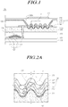
- FIG. 1 is a cross-sectional view of a top emission type organic light emitting diode display device according to one exemplary aspect.
- FIG. 2A is an enlarged cross-sectional view of area X of FIG. 1 .
- FIG. 2B is a partial plan view of an overcoating layer in area X of FIG. 1 .
- an organic light emitting diode display device 100 preferably of a top emission type, according to one exemplary aspect includes a substrate 110, a thin film transistor 120, an overcoating layer 160, an organic light emitting diode 140, and a color filter 150.
- the top emission type organic light emitting diode display device 100 illustrated in FIGs. 1 and 2A is described as being an organic light emitting diode display device in an upper emission type or a top emission type, in which the color filter 150 is positioned at a side opposite to the substrate 110.
- an organic light emitting diode display device may be a lower emission type or a bottom emission type, in which the color filter 150 is positioned at the substrate 110 side.
- the top emission type organic light emitting diode display device 100 has an aperture ratio greater than that of the bottom emission type organic light emitting diode display device, and thus has an advantage in a life span and luminance.
- the thin film transistor 120 including a gate electrode 121, an active layer 122, a source electrode 123 and a drain electrode 124, is disposed on the substrate 110.
- the gate electrode 121 is disposed on the substrate 110, a gate insulating layer 131 for insulating the gate electrode 121 from the active layer 122 is disposed on the gate electrode 121 including the substrate 110, the active layer 122 is disposed on the gate insulating layer 131, an etch stopper 132 is disposed on the active layer 122, and the source electrode 123 and the drain electrode 124 are disposed on the active layer 122 and the etch stopper 132.
- the source electrode 123 and the drain electrode 124 in a manner of being in contact with the active layer 122 are electrically connected to the active layer 122, and are disposed on a portion of the etch stopper 132.
- the etch stopper 132 may not be disposed.
- the thin film transistor 120 is described as having an inverted staggered structure or a bottom gate structure, in which the gate electrode 121 is positioned at a side opposite to the source electrode 123 and the drain electrode 124 with respect to the active layer 122, but a thin film transistor having a coplanar structure or a top gate structure, in which the gate electrode 121 is positioned at a side, at which the source electrode 123 and the drain electrode 124 are positioned, with respect to the active layer 122, may be used.
- a passivation layer 133 is illustrated as planarizing an upper portion of the thin film transistor 120 in FIG. 1 , the passivation layer 133 may not planarize the upper portion of the thin film transistor 120 and may be disposed along surface shapes of elements positioned thereunder.
- the overcoating layer 160 is disposed on the passivation layer 133.
- the passivation layer 133 is illustrated as being included in the top emission type organic light emitting diode display device 100 in FIG. 1 , the passivation layer 133 may not be used and the overcoating layer 160 may be directly disposed on the thin film transistor 120.
- the overcoating layer 160 includes a plurality of convex portions 162 and first connection portions 161 which connect adjacent convex portions 162.
- the first connection portion 161 is a portion positioned between adjacent convex portions 162.
- the overcoating layer 160 functions as a planarizing layer at portions in which the plurality of convex portions 162 are not disposed.
- each of the plurality of convex portions 162 and the first connection portions 161 may have a generally circular shape in a plan view, but the present disclosure is not limited thereto, and may have various shapes such as a generally hemispherical shape, a semi-ellipsoidal shape, a rectangular shape, a hexagonal shape, and the like.
- the plurality of convex portions 162 may be disposed in a circular shape in a plan view.
- the convex portion 162 having a circular shape and another convex portion 162 adjacent thereto may be disposed in a circular-shaped structure to be integrally formed with one shared side.
- a bank layer 136 and the organic light emitting diode 140 including a first electrode 141, an organic light emitting layer 142, and a second electrode 143 are disposed on the overcoating layer 160.
- an insulating second passivation layer (not illustrated) may be added between the overcoating layer 160 and the first electrode 141 so as to have a shape depending on a morphology of the convex portion 162 of the overcoating layer 160 while preventing outgas from being diffused from the overcoat layer 160 to the organic light emitting diode 140 and to have a refractive index similar to that of the first electrode 141.
- the first electrode 141 for supplying one among electrons and holes to the organic light emitting layer 142 is disposed on a portion of the overcoating layer 160.
- the first electrode 141 may be a positive electrode, a pixel electrode or an anode in a normal organic light emitting diode (OLED), and may be a negative electrode, a pixel electrode or a cathode in an inverted OLED.
- a reflection plate 141a formed of, for example, a conductive material is included at a lower portion of the first electrode 141.
- the reflection plate 141a may reflect light emitted from the organic light emitting layer 142 to improve top light emission efficiency.
- the first electrode 141 itself functions as a reflection plate, a separate reflection plate 141a may not be included at the lower portion of the first electrode 141.
- the reflection plate 141a When the reflection plate 141a is included at the lower portion of the first electrode 141, the reflection plate 141a may be patterned in the same manner as the first electrode 141. Therefore, the first electrode 141 and the reflection plate 141a may function as multiple electrodes. Further, the first electrode 141 may be a multiple electrode including multiple layers, for example, double electrodes, and the reflection plate 141a may be included in the multilayered first electrode 141.
- the reflection plate 141a is included at the lower portion of the first electrode 141 and the first electrode 141 and the reflection plate 141a function as multiple electrodes will be described.
- the reflection plate 141a and the first electrode 141 may be connected to the source electrode 123 of the thin film transistor 120 through a contact hole formed in the overcoating layer 160.
- the first electrode 141 is described as being connected to the source electrode 123 assuming a case in which the thin film transistor 120 is an N-type thin film transistor, but the reflection plate 141a and the first electrode 141 may be connected to the drain electrode 124 in a case in which the thin film transistor 120 is a P-type thin film transistor.
- the first electrode 141 may be in direct contact with the organic light emitting layer 142, or may be electrically connected to the organic light emitting layer 142 to be in contact therewith, with a conductive material interposed therebetween.
- the reflection plate 141a and the first electrode 141 are disposed to have a shape depending on a morphology of a surface of the overcoating layer 160. Therefore, the reflection plate 141a and the first electrode 141 have a convex morphology at the convex portion 162 of the overcoating layer 160.
- the bank layer 136 including an opening 136a through which the first electrode 141 is exposed is disposed on the overcoating layer 160, the reflection plate 141a, and the first electrode 141.
- the bank layer 136 may serve to distinguish adjacent pixel areas (or sub pixel areas), and may be disposed between adjacent pixel areas (or sub pixel areas).
- the convex portion 162 and the first connection portion 161 of the overcoating layer 160 are disposed to overlap the opening 136a of the bank layer 136. Since the convex portion 162 and the first connection portion 161 of the overcoating layer 160 arc disposed to overlap the color filter 150 to be described below, the convex portion 162 and the first connection portion 161 of the overcoating layer 160 overlap the opening 136a of the bank layer 136, and the color filter 150 above.
- the organic light emitting layer 142 is disposed on the first electrode 141, and the second electrode 143 for supplying one among electrons and holes to the organic light emitting layer 142 is disposed on the organic light emitting layer 142.
- the organic light emitting layer 142 is disposed in a structure (e.g., a tandem white structure) in which a plurality of organic light emitting layers are stacked in order to emit white light.
- the organic light emitting layer 142 includes a first organic light emitting layer which emits blue light and a second organic light emitting layer which is disposed on the first organic light emitting layer and emits light having a color that becomes white by being mixed with blue.
- the second organic light emitting layer may be, for example, an organic light emitting layer which emits yellow-green light.
- the organic light emitting layer 142 may include only an organic light emitting layer which emits one of blue light, red light, and green light.
- the color filter 150 may not be included therein.
- the second electrode 143 may be a negative electrode, a common electrode, or a cathode in a normal OLED, and may be a positive electrode, a common electrode or an anode in an inverted OLED.
- the color filter 150 When the color filter 150 is included therein, the color filter 150 is disposed on the second electrode 143. An adhesion layer 170 may be included between the second electrode 143 and the color filter 150.
- the color filter 150 is for converting a color of light emitted from the organic light emitting layer 142, and may be one of a red color filter, a green color filter, and a blue color filter.
- the color filter 150 is disposed at a position corresponding to an emission area on the second electrode 143.
- the emission area refers to an area in which the organic light emitting layer 142 emits light by the first electrode 141 and the second electrode 143, and that the color filter 150 is disposed at a position corresponding to the emission area signifies that the color filter 150 is disposed so as to prevent a blurring phenomenon and a ghost phenomenon from occurring by mixing lights emitted from adjacent emission areas.
- the color filter 150 is disposed to overlap the emission area, and specifically, may have a size less than or equal to that of the emission area.
- a size and arrangement position of the color filter 150 may be determined by various factors such as a size and position of the emission area, a distance between the color filter 150 and the second electrode 143, a distance between the emission areas, and the like.
- a thickness of the organic light emitting layer 142 between the convex portion 162 and the first connection portion 161 of the overcoating layer 160 may be smaller than a thickness of the organic light emitting layer 142 at a bottom of the convex portion 162 of the overcoating layer 160 or at a top of the first connection portion 161.
- the thickness of the organic light emitting layer 142 may be smallest at a position at which a slope of the organic light emitting layer 142 between the convex portion 162 and the first connection portion 161 of the overcoating layer 160 is largest.
- a thickness of the organic light emitting layer 142 deposited in a direction perpendicular to the substrate 110 is the same, but the organic light emitting layer 142 may have a shape depending on a morphology of the overcoating layer 160. Due to characteristics of the deposition process, a thickness d1 of the organic light emitting layer 142 which drives a current between the first electrode 141 and the second electrode 143 is smallest at a position at which the slope of the organic light emitting layer 142 is largest.
- Thicknesses d2 and d3 of the organic light emitting layer 142 which drives a current between the first electrode 141 and the second electrode 143 is largest at a position at which the slope of the organic light emitting layer 142 is smallest, that is, at a bottom or top thereof.
- an amount of emission per unit area of the organic light emitting layer 142 between the convex portion 162 and the first connection portion 161 of the overcoating layer 160 may be greater than an amount of emission per unit area of the organic light emitting layer 142 at the bottom of the convex portion 162 or at the top of the first connection portion 161.
- the amount of emission of the organic light emitting layer 142 may be the largest at a position at which the slope of the organic light emitting layer 142 between the convex portion 162 and the first connection portion 161 of the overcoating layer 160 is largest.
- the organic light emitting layer 142 and the second electrode 143 are disposed to have a shape depending on the morphology of the surface of the overcoating layer 160.
- a shape of the organic light emitting diode 140 having a micro lens array structure may be implemented using the convex portion 162 of the overcoating layer 160.
- the organic light emitting diode 140 has a micro lens array structure for improving an external light extraction efficiency
- a convex curvature is generated on the surface of the organic light emitting diode 140 by the convex portion 162 of the overcoating layer 160 as illustrated in FIG. 2A due to a characteristic of the pattern.
- a thinnest thickness d1 of the organic light emitting layer 142 between the first electrode 141 and the second electrode 143 is reduced in the area having a large slope, an efficient emission area Y in which electric fields are locally concentrated, that is, an area between the convex portion 162 and the first connection portion 161 of the overcoating layer 160, is formed.
- the organic light emitting diode 140 When the organic light emitting diode 140 is driven, the electric fields are locally concentrated in such an efficient emission area, a main current path is formed, and the main emission occurs.
- light is rarely extracted in an inefficient emission area Z in the convex portion 162 of the overcoating layer 160. In the inefficient emission area Z, light is rarely extracted despite power consumption, and thus the external light extraction efficiency is reduced.
- a micro lens array pattern having a convex shape may be included in the overcoating layer 160.
- Light emitted from the organic light emitting layer 142 is locked in the organic light emitting layer 142 and the second electrode 143 while being totally reflected, but the light travels at an angle smaller than a critical angle for total reflection by the inserted micro lens array structure, and thus the external light emission efficiency may be increased by multiple reflections.
- a traveling angle of the light emitted from the organic light emitting layer 142 is changed by the inserted micro lens array pattern, and the traveling angle of the light may be clearly changed even by a minute difference in a shape of the micro lens array.
- the shape of the convex portion 162 of the overcoating layer 160 is formed through a process such as a photolithography process and the like, and the morphology of the convex portion 162 of the overcoating layer 160 may be adjusted by controlling a heat treatment process performed at this time.
- a material of the overcoating layer 160 may be a general positive or negative photoresist.
- the material of the overcoating layer 160 may be a negative photoresist in which an exposed portion is cured.
- the convex portion 162 of the overcoating layer 160 is patterned in a convex shape through a photolithography process by being coated with a photoresist, and heat treatment is then performed thereon.
- the shape of the convex portion 162 of the overcoating layer 160 may be formed by sequentially performing the heat treatment in two steps rather than performing the heat treatment at one time. For example, an intermediate heat treatment at a temperature ranging from about 100 °C to about 130 °C should be performed before the final heat treatment at a temperature ranging from about 200 °C to about 250 °C is performed.
- a time for which the intermediate heat treatment is performed is related to the morphology of the convex portion 162 of the overcoating layer 160.
- the morphology of the finally formed convex portion 162 of the overcoating layer 160 is increased.
- the morphology of the convex portion 162 of the overcoating layer 160 disappears and the overcoating layer 160 is planarized.
- various top emission type organic light emitting diode display devices having different morphologies of the convex portion 162 of the overcoating layer 160 are formed.
- these top emission type organic light emitting diode display devices when the convex portion 162 of the overcoating layer 160 had a certain morphology, that is, when the convex portion 162 of the overcoating layer 160 had a certain aspect ratio value, it was experimentally examined whether the organic light emitting diode 140 can be operated with maximum light emission efficiency.
- top emission type organic light emitting diode display device 100 In the top emission type organic light emitting diode display device 100 according to one exemplary aspect, light which is totally reflected and locked in the organic light emitting diode 140 is extracted to the outside through a light path changed according to the shape of the convex portion 162 of the overcoating layer 160 which is inserted for improving the external light extraction efficiency.
- FIG. 3A is a view conceptually illustrating variables on which a shape of a convex portion of an overcoating layer depends.
- FIG. 3B is a view illustrating variables determining the shape of the convex portion of the overcoating layer in the top emission type organic light emitting diode display device according to one exemplary aspect.
- FIG. 3C is a view for describing the concept of gap G at a bottom of the convex portion of the overcoating layer.
- a diameter D of the convex portion 162 of the overcoating layer 160 refers to a length between centers of two first connection portions 161, and a height H refers to a length from the bottom of the convex portion 162 to the top of the convex portion 162.
- a full width at half maximum F refers to a length between both sides of the convex portion 162 at a position of a half-height H/2 as illustrated in FIG. 3A .
- An aspect ratio (A/R) of the convex portion 162 refers to a value obtained by dividing the height H of the convex portion 162 by a radius D/2 of the convex portion 162.
- the convex portion 162 may have a circular shape in which a diameter D ranges from about 1 ⁇ m to 5 ⁇ m and a height H ranges from about 1 ⁇ m to 4 ⁇ m.
- a current efficiency enhancement is more excellent in the case in which the aspect ratio A/R of the convex portion 162 of the overcoating layer 160 has a value ranging from about 0.35 to about 0.8 than in the case in which the aspect ratio A/R of the convex portion 162 of the overcoating layer 160 has a value more than 0.8. It can be confirmed that the current efficiency enhancement is rather reduced in the case in which the aspect ratio A/R of the convex portion 162 of the overcoating layer 160 has a value more than 0.8. Specifically, it can be seen that the current efficiency enhancement is maximum in the case in which the aspect ratio A/R of the convex portion 162 of the overcoating layer 160 has a value ranging from about 0.4 to about 0.7.
- a surface on which the organic light emitting diode 140 is disposed may be an upper surface of the overcoating layer 160 in which the aspect ratio A/R of the convex portion 162 of the overcoating layer 160 has a value ranging from about 0.35 to about 0.8.
- a surface on which the organic light emitting diode 140 is disposed may be an upper surface of a second passivation layer (not illustrated) depending on the morphology of the overcoating layer 160 in which the aspect ratio A/R of the convex portion 162 of the overcoating layer 160 has a value ranging from about 0.35 to about 0.8.
- the overcoating layer 160 or the second passivation layer (not illustrated) is a smooth non-flat plane in which an aspect ratio A/R of a surface has a value ranging from about 0.35 to about 0.8, and thus the organic light emitting diode 140 is formed on a smooth non-flat plane in which an aspect ratio has a value ranging from about 0.35 to about 0.8. Therefore, the first electrode 141, the organic light emitting layer 142, and the second electrode 143 have a shape depending on the morphology of the smooth non-flat plane.
- an intermediate heat treatment process is necessarily performed in a short time when the convex portion 162 of the overcoating layer 160 is formed, and thus the convex portion 162 of the overcoating layer 160 may be formed to have a smooth slope.
- the overcoating layer 160 is formed so that the aspect ratio A/R of the convex portion 162 of the overcoating layer 160 has a value ranging from about 0.35 to about 0.8 through such a method
- the bank layer 136 and the organic light emitting diode 140 including the first electrode 141, the organic light emitting layer 142, and the second electrode 143 may be formed on the overcoating layer 160.
- the shape of the convex portion 162 of the overcoating layer 160 is significantly changed when values defined by the full width at half maximum F or the other variables such as gap G between the convex portions and the like are changed as illustrated in FIG. 3C .
- FIG. 4 is a cross-sectional view of a convex portion 162 of an overcoating layer 160 having a specific aspect ratio.
- An aspect ratio A/R of the convex portion 162 of the overcoating layer 160 illustrated in FIG. 4 is set to about 0.45, and is included in a range of about 0.35 to about 0.8 of the convex portion 162 of the overcoating layer 160 having an excellent current efficiency enhancement as described above.
- the organic light emitting diode 140 has a micro lens array structure for improving the external light extraction efficiency, since a thinnest thickness d1 of the organic light emitting layer 142 between the first electrode 141 and the second electrode 143 is reduced in an area of the convex portion 162 of the overcoating layer 160 having a large slope S due to a characteristic of the pattern, an efficient emission area Y in which electric fields are locally concentrated, that is, an area between the convex portion 162 and the first connection portion 161 of the overcoating layer 160, is formed.
- a maximum slope Smax of the convex portion 162 is positioned at a position at which the organic light emitting layer 142 has a thinnest thickness d1.
- FIGs. 5A and 5B illustrate various shapes of a convex portion of an overcoating layer having the same or similar aspect ratio (A/R).
- a full width at half maximum F of the convex portion 162 of the overcoating layer 160 is a half diameter D/2.
- the convex portion 162 of the overcoating layer 160 included in the top emission type organic light emitting diode display device 100 may have a full width at half maximum F greater than a radius D/2.
- FIG. 5B a comparison of a convex portion 162 of an overcoating layer 160 having a shape in which a full width at half maximum F is greater than a radius D/2 and a convex portion 162a of an overcoating layer 160 having a shape in which a full width at half maximum F is smaller than a radius D/2 is illustrated.
- a light path on which light emitted from the organic light emitting layer 142 at the same position is reflected by the convex portion 162a having a shape different from that of the convex portion 162 of the overcoating layer 160 is illustrated.
- the full width at half maximum F of the convex portion 162 of the overcoating layer 160 is greater than the radius D/2 thereof signifies that the convex portion 162 is formed wider between side surfaces, a light path in a direction of a side surface of the reflection plate 141a is reduced, and thus an external light extraction efficiency may be improved.
- the full width at half maximum F of the convex portion 162a of the overcoating layer 160 is smaller than the radius D/2 signifies that the convex portion 162a is formed thinner between side surfaces, a light path in the direction of the side surface of the reflection plate 141a is increased, and thus the external light extraction efficiency may be rcduccd.
- the convex portion 162 of the overcoating layer 160 having a shape in which a full width at half maximum F is greater than a radius D/2, a light path in the direction of the side surface of the reflection plate 141a is reduced, and thus the external light extraction efficiency may be improved.
- a ratio of the full width at half maximum F with respect to the radius D/2 of the convex portion 162 may be about 1.0 or more.
- FIG. 6 is a graph illustrating a relationship between current efficiency enhancements (%) or enhancements of current efficiency (%) and a full width at half maximum in respective top emission type organic light emitting diode display devices having various values of the full width at half maximum of a convex portion 162 of an overcoating layer 160.
- a high current efficiency enhancement means an excellent light emission efficiency.
- a height H is about 1.7 2. ⁇ m, and an aspect ratio A/R is 0.76
- current efficiency enhancement is more excellent in the case in which the full width at half maximum F is about 2.0 ⁇ m or more than in the case in which the full width at half maximum F is less than about 2.0 ⁇ m. It may be confirmed that the current efficiency enhancement is rather reduced (i.e., the current efficiency enhancement has a negative value) in the case in which the full width at half maximum F of the convex portion 162 of the overcoating layer 160 has a value less than about 2.0 ⁇ m.
- the aspect ratio A/R of the convex portion 162 of the overcoating layer 160 has an optimal value
- the full width at half maximum F has a value less than about 2.0 um
- an angle of light which travels inside the organic light emitting diode 140 becomes greater than or equal to a critical angle for total reflection at which light should be locked between the substrate 110 and the organic light emitting layer 142. Therefore, it may be confirmed that the current efficiency enhancement is rather reduced, and thus the light emission efficiency is reduced.
- an aspect ratio at half maximum F_A/R of the convex portion 162 may be smaller than an aspect ratio A/R.
- the aspect ratio at half maximum F_A/R of the convex portion 162 refers to a height H with respect to the full width at half maximum F of the convex portion 162. That is, the aspect ratio at half maximum with respect to the aspect ratio of the convex portion 162 may be smaller than 1.0.
- the aspect ratio at half maximum F_A/R of the convex portion 162 may be, for example, more than 0.30 and 0.6 or less.
- the convex portion 162 of the overcoating layer 160 may have various shapes even when a full width at half maximum F is greater than a radius D/2 and the full width at half maximum F is the same.
- the convex portion 162 of the overcoating layer 160 having the full width at half maximum F greater than the radius D/2 may have a shape in which a slope S of the convex portion 162 of the overcoating layer 160 is gradually increased at a bottom with respect to a left upper surface and is gradually decreased again after reaching a maximum slope Smax (i.e., the shape of the convex portion 162 of FIG. 5A ).
- an amount of emission of the organic light emitting layer 142 is largest at a position at which a slope of the organic light emitting layer 142 between the convex portion 162 and the first connection portion 161 of the overcoating layer 160 is largest, that is, at a maximum slope Smax.
- the top emission type organic light emitting diode display device 100 when the top emission type organic light emitting diode display device 100 according to one exemplary aspect has a shape in which the slope of the convex portion 162 of the overcoating layer 160 is increased at the bottom and is decreased at the maximum slope (i.e., the shape of the convex portion 162 of FIG. 5A ), light emitted from the organic light emitting layer 142 travels at an angle smaller than a critical angle for total reflection, the external light emission efficiency is increased by multiple reflections, and thus maximum external light extraction efficiency may be obtained.
- the external light extraction efficiency may be increased.
- the gap G at the bottom of the convex portion 162 is 0.
- the gap G is greater than 0, a gap is present between two adjacent first connection portions 161, and because an efficient emission area is reduced, the light emission efficiency may be reduced by an area of the gap G.
- FIG. 7 is a view illustrating a light path according to a maximum slope of a convex portion of an overcoating layer.
- the convex portion 162 of the overcoating layer 160 may have a shape in which the slope is increased at the bottom and is decreased at the maximum slope Smax (i.e., the shape of the convex portion 162 of FIG. 5A ) as illustrated in FIG. 5A .
- the convex portion 162 of the overcoating layer 160 may have various shapes according to an angle of the maximum slope.
- the convex portion 162 of the overcoating layer 160 has a shape in which the maximum slope Smax has a high angle more than 60 degrees, for example, 70 degrees (i.e., Smax is 70 degrees)
- a traveling angle of light starting from the efficient emission area becomes 42 degrees or more, as a result, the light is locked in the organic light emitting diode 140, and thus the light emission efficiency may not be increased.
- the convex portion 162 of the overcoating layer 160 has a shape in which the maximum slope Smax of the convex portion 162 has an angle ranging from 40 degrees to 60 degrees (e.g., 50 degrees)
- light emitted from the organic light emitting layer 142 is not locked in the organic light emitting diode 140 in view of the traveling angle of light starting from the efficient emission area, and thus the light emission efficiency may be increased.
- FIG. 8 is a graph illustrating a relationship between current efficiency enhancements (%) or enhancements of current efficiency (%) and a maximum slope Smax in respective top emission type organic light emitting diode display devices having various values of the maximum slope Smax of the convex portion 162 of the overcoating layer 160.
- the maximum slope Smax of the convex portion 162 of the overcoating layer 160 is less than 40 degrees, because a traveling angle of light in the efficient emission area is not significantly different from a flat organic light emitting diode of the overcoating layer 160, it was confirmed that there is little improvement in efficiency. Further, when the maximum slope Smax of the convex portion 162 of the overcoating layer 160 is more than 60 degrees, a traveling angle of light is greater than a total reflection angle between the substrate 110 and an air layer outside the substrate 110, an amount of light locked in the organic light emitting diode 140 is significantly increased, and thus a result in which the efficiency is somewhat reduced compared to that of the flat organic light emitting diode of the overcoating layer 160 was shown.
- the shape of the convex portion 162 of the overcoating layer 160 illustrated in FIG. 4 has a maximum slope Smax of the convex portion 162 ranging from 40 degrees to 60 degrees, light emitted from the organic light emitting layer 142 is not locked in the organic light emitting diode 140 in view of the traveling angle of light starting from the efficient emission area, and thus the light emission efficiency may be increased.
- FIG. 9 illustrates an area having a maximum slope according to an aspect ratio at half maximum Rm with respect to an aspect ratio of a convex portion.
- the aspect ratio at half maximum Rm with respect to the aspect ratio of the convex portion 162 is a ratio of an aspect ratio at half maximum F_A/R and an aspect ratio A/R, and may be a variable on which an area having a sharpest maximum slope Smax depends.
- a first area C is an area having a maximum slope Smax.
- a second area B is an area having a maximum slope Smax.
- a third area A is an area having a maximum slope Smax.
- the overcoating layer 160 includes the convex portion 162
- the light extraction efficiency or the light emission efficiency according to the shape of the convex portion 162 has been described.
- the case in which the external light extraction efficiency or the light emission efficiency according to a shape of a concave portion is obtained in the same manner as the convex portion 162 even when the overcoating layer 160 includes the concave portion will be described with reference to FIG. 10 .
- FIG. 10 is a cross-sectional view for describing a top emission type organic light emitting diode display device including an overcoating layer having a plurality of concave portions according to another exemplary aspect.
- an overcoating layer 260 includes a plurality of concave portions 264 unlike the top emission type organic light emitting diode display device 100 of FIGs. 1 to 2B , since the other components are the same, redundant description thereof will be omitted.
- Elements of the organic light emitting display device 200 which are not illustrated in FIG. 10 may be the same as the above-described elements of the top emission type organic light emitting diode display device 100 according to one exemplary aspect.
- the overcoating layer 260 includes the plurality of concave portions 264 and second connection portions 263 which connect adjacent concave portions 264.
- the overcoating layer 260 includes the plurality of concave portions 264 which are disposed to overlap the opening 136a of the bank layer 136 illustrated in FIG. 1 , and the plurality of second connection portions 263 which connect the concave portions 264.
- a reflection plate 241a and a first electrode 241 are disposed on the overcoating layer 260.
- An organic light emitting layer 242 and a second electrode 243 are disposed on the overcoating layer 260 and the first electrode 241.
- the first electrode 241, the organic light emitting layer 242, and the second electrode 243 may constitute an organic light emitting diode 240.
- a color filter (not illustrated) which is disposed to overlap the concave portions 264 and the second connection portions 263 which connect adjacent concave portions 264 is disposed on the second electrode 243.
- the reflection plate 241a, the first electrode 241, the organic light emitting layer 24, and the second electrode 243 may be disposed along a shape of an upper surface of the overcoating layer 260, and may have a shape depending on a morphology of the overcoating layer 260.
- a full width at half maximum F of the convex portion 162 of the overcoating layer 160 may be greater than a radius D/2.
- a ratio of the full width at half maximum F with respect to a radius D/2 of the concave portion 264 may be 1.0 or more.
- an aspect ratio at half maximum F_A/R of the convex portion 162 of the overcoating layer 160 may be smaller than an aspect ratio A/R.
- the aspect ratio at half maximum F_A/R with respect to the aspect ratio A/R of the concave portion 264 may be smaller than 1.0.
- the concave portion 264 may have a hexagonal shape in which a diameter ranges from about 1 ⁇ m to about 5 ⁇ m and a height ranges from about 1 ⁇ m to about 4 ⁇ m.
- the aspect ratio of the concave portion 264 may range from 0.35 to 0.8 and the aspect ratio at half maximum thereof may range from 0.30 to 0.60, but the present disclosure is not limited thereto.
- the concave portion 264 of the overcoating layer 260 may have a shape in which a slope is increased at a bottom and is then gradually reduced at a maximum slope.
- a maximum slope of the concave portion 264 of the overcoating layer 260 may range from 40 degrees to 60 degrees.
- the overcoating layer 260 includes the concave portion 264 is described as having external light extraction efficiency or light emission efficiency according to the shape of the concave portion 264 like the case in which the convex portion 162 of the overcoating layer 160 of the top emission type organic light emitting diode display device 100 described with reference to FIG. 1 , but the shapes of the concave portion 264 and the second connection portion 263 according to the omitted variables are the same as those described above with reference to the convex portion 162 and the first connection portion 262.
- FIG. 11 is a schematic diagram illustrating a configuration of a top emission type organic light emitting diode display device according to exemplary aspects.
- a top emission type organic light emitting diode display device 300 includes an organic light emitting display panel 310, a data driver 320, a gate driver 330, and a controller 340.
- the organic light emitting display panel 310 includes a plurality of data lines DLs, a plurality of gate lines GLs, and a plurality of sub pixels SPs which is disposed in a matrix form.
- the data driver 320 drives the plurality of data lines by supplying a data voltage to the plurality of data lines.
- the gate driver 330 subsequently drives the plurality of gate lines by sequentially supplying a scanning signal to the plurality of gate lines.
- the controller 340 controls the data driver 320 and the gate driver 330.
- the thin film transistor and the organic light emitting diode which are described with reference to FIG. 1 are included in each of a plurality of pixels disposed on the organic light emitting display panel 310 according to the exemplary aspects.
- a micro lens array structure may be applied to the top emission type organic light emitting diode display device so that external light extraction efficiency may be improved.
- the top emission type organic light emitting diode display device may improve external light emission efficiency and reduce power consumption.
- a life span of the top emission type organic light emitting diode display device may be increased.
Landscapes
- Engineering & Computer Science (AREA)
- Microelectronics & Electronic Packaging (AREA)
- Electroluminescent Light Sources (AREA)
Claims (14)
- Dispositif d'affichage à diodes électroluminescentes organiques, comportant :des régions de pixels au-dessus d'un substrat (11) ;une couche de revêtement de finition (160, 260) sur les régions de pixels du substrat, la couche de revêtement de finition (160, 260) ayant au moins une partie parmi une pluralité de parties convexes (162) et une pluralité de parties concaves (264), chacune ayant une largeur totale à mi-hauteur (F) supérieure à un rayon (D/2) ;une première électrode (141, 241) disposée au-dessus de la couche de revêtement de finition (160, 160) ;une couche électroluminescente organique (142, 242) disposée sur la première électrode (141, 242), etune plaque de réflexion (141a, 241a) disposée entre la première électrode (141, 241) et la couche de revêtement de finition (160, 260),dans lequel la couche de revêtement de finition (160, 260) inclut en outre une partie d'aplatissement entre les régions de pixels,dans lequel le rayon (D/2) est égal à la moitié d'un diamètre (D), le diamètre (D) étant une longueur entre deux centres de deux parties de liaison (161, 263), qui relient des parties convexes (162) ou des parties concaves (264) adjacentes,dans lequel la largeur totale à mi-hauteur (F) est une longueur entre deux côtés de la partie convexe ou concave (162, 264) à une position d'une demie hauteur (H/2), qui est la moitié d'une hauteur (H) correspondant à une longueur depuis un bas de cette partie (162, 264) jusqu'au sommet de cette partie (162, 264).
- Dispositif d'affichage à diodes électroluminescentes organiques selon la revendication 1, dans lequel la plaque de réflexion (141a, 241a) sur la couche de revêtement de finition (160, 260) correspond sensiblement à un contour d'une surface supérieure de la couche de revêtement de finition (160, 260).
- Dispositif d'affichage à diodes électroluminescentes organiques selon l'une des revendications précédentes, dans lequel chacune des parties convexes (162) ou des parties concaves (264) a un rapport d'aspect (A/R) variant d'environ 0,35 à environ 0,8, le rapport d'aspect (A/R) étant un quotient entre la hauteur (H) et le rayon (D/2), et un rapport d'aspect (F_A/R) à mi-hauteur (F) variant d'environ 0,30 à environ 0,60, le rapport d'aspect (F_A/R) à mi-hauteur (F) étant un quotient entre la hauteur (H) et la largeur totale à mi-hauteur (F).
- Dispositif d'affichage à diodes électroluminescentes organiques selon l'une des revendications précédentes, dans lequel chacune des parties convexes (162) ou des parties concaves (264) a un rapport de la largeur totale à mi-hauteur (F) sur le rayon (D/2) supérieur à 1,0.
- Dispositif d'affichage à diodes électroluminescentes organiques selon l'une des revendications précédentes, dans lequel chacune des parties convexes (162) ou des parties concaves (264) a un rapport d'aspect (A/R) à la largeur totale à mi-hauteur (F) inférieur à un rapport d'aspect (A/R) de celle-ci.
- Dispositif d'affichage à diodes électroluminescentes organiques selon l'une des revendications précédentes, dans lequel chacune des parties convexes (162) ou des parties concaves (264) a une pente maximale (Smax) variant d'environ 40 degrés à environ 60 degrés.
- Dispositif d'affichage à diodes électroluminescentes organiques selon l'une des revendications précédentes, dans lequel le dispositif d'affichage à diodes électroluminescentes organiques est un dispositif d'affichage à diodes électroluminescentes organiques de type à émission par le dessus, comportant :la couche de revêtement de finition (160, 260) disposée au-dessus d'un substrat (110) ; etune seconde électrode (143, 243) disposée sur la couche électroluminescente organique (142, 242).
- Dispositif d'affichage à diodes électroluminescentes organiques selon la revendication 7, comportant en outre un filtre à couleur (150) disposé sur la seconde électrode (143, 243).
- Dispositif d'affichage à diodes électroluminescentes organiques selon la revendication 7 ou 8, dans lequel la plaque de réflexion (141a, 241a), la première électrode (141, 241), la couche électroluminescente organique (142, 242) et la seconde électrode (143, 243) sont disposées pour correspondre à une forme d'une surface supérieure de la couche de revêtement de finition (160, 260), et ont une forme déterminée par une morphologie de la couche de revêtement de finition (160, 260).
- Dispositif d'affichage à diodes électroluminescentes organiques selon l'une des revendications 5 à 9, dans lequel chacune des parties convexes (162) ou des parties concaves (264) a un rapport du rapport d'aspect (A/R) à la largeur totale à mi-hauteur (F) sur le rapport d'aspect (A/R) de celle-ci soit inférieur à 1,0.
- Dispositif d'affichage à diodes électroluminescentes organiques selon l'une des revendications 7 à 10, dans lequel chacune des parties convexes (162) ou des parties concaves (264) a une forme circulaire avec un diamètre (D) variant d'environ 1 µm à environ 5 µm et une hauteur (H) variant d'environ 1 µm à environ 4 µm.
- Dispositif d'affichage à diodes électroluminescentes organiques selon l'une des revendications 7 à 11, dans lequel chacune des parties convexes (162) ou des parties concaves (264) a une forme avec une pente (S) augmentant à partir d'une partie inférieure et diminuant à une pente maximale (Smax).
- Dispositif d'affichage à diodes électroluminescentes organiques selon l'une des revendications 7 à 12, dans lequel chacune des parties convexes (162) ou des parties concaves (264) a une pente maximale (Smax) positionnée au niveau d'une troisième zone, qui est adjacente à un sommet de première à troisième zones qui sont coupées en trois parties égales à partir d'un bas par rapport à une hauteur de celle-ci, dans lequel la couche électroluminescente organique (142) a de préférence une amélioration de rendement en courant maximale au niveau de la troisième zone.
- Dispositif d'affichage à diodes électroluminescentes organiques selon l'une des revendications précédentes, dans lequel la couche de revêtement de finition (160, 260) est formée d'une résine photosensible négative ayant une partie exposée devant être durcie, et/ou dans lequel la première électrode (141) et la plaque de réflexion (141a, 241a) fonctionnent comme une électrode multiple.
Priority Applications (1)
| Application Number | Priority Date | Filing Date | Title |
|---|---|---|---|
| EP16207219.3A EP3343659B1 (fr) | 2016-12-29 | 2016-12-29 | Afficheur à diode électroluminescente organique de type à émission supérieure |
Applications Claiming Priority (1)
| Application Number | Priority Date | Filing Date | Title |
|---|---|---|---|
| EP16207219.3A EP3343659B1 (fr) | 2016-12-29 | 2016-12-29 | Afficheur à diode électroluminescente organique de type à émission supérieure |
Publications (2)
| Publication Number | Publication Date |
|---|---|
| EP3343659A1 EP3343659A1 (fr) | 2018-07-04 |
| EP3343659B1 true EP3343659B1 (fr) | 2021-06-16 |
Family
ID=57680150
Family Applications (1)
| Application Number | Title | Priority Date | Filing Date |
|---|---|---|---|
| EP16207219.3A Active EP3343659B1 (fr) | 2016-12-29 | 2016-12-29 | Afficheur à diode électroluminescente organique de type à émission supérieure |
Country Status (1)
| Country | Link |
|---|---|
| EP (1) | EP3343659B1 (fr) |
Families Citing this family (1)
| Publication number | Priority date | Publication date | Assignee | Title |
|---|---|---|---|---|
| KR102328085B1 (ko) * | 2017-11-30 | 2021-11-17 | 엘지디스플레이 주식회사 | 전계발광 표시장치 |
Citations (1)
| Publication number | Priority date | Publication date | Assignee | Title |
|---|---|---|---|---|
| KR20160080834A (ko) * | 2014-12-29 | 2016-07-08 | 엘지디스플레이 주식회사 | 유기 발광 표시 장치 및 유기 발광 표시 장치 제조 방법 |
Family Cites Families (3)
| Publication number | Priority date | Publication date | Assignee | Title |
|---|---|---|---|---|
| JP2011076774A (ja) * | 2009-09-29 | 2011-04-14 | Sony Corp | 発光装置および表示装置 |
| WO2012060404A1 (fr) * | 2010-11-02 | 2012-05-10 | 王子製紙株式会社 | Diode électroluminescente organique, procédé de fabrication de celle-ci, dispositif d'affichage d'images et dispositif d'éclairage |
| CN103000639B (zh) * | 2012-12-12 | 2016-01-27 | 京东方科技集团股份有限公司 | 阵列基板及其制备方法、有机发光二极管显示装置 |
-
2016
- 2016-12-29 EP EP16207219.3A patent/EP3343659B1/fr active Active
Patent Citations (1)
| Publication number | Priority date | Publication date | Assignee | Title |
|---|---|---|---|---|
| KR20160080834A (ko) * | 2014-12-29 | 2016-07-08 | 엘지디스플레이 주식회사 | 유기 발광 표시 장치 및 유기 발광 표시 장치 제조 방법 |
Also Published As
| Publication number | Publication date |
|---|---|
| EP3343659A1 (fr) | 2018-07-04 |
Similar Documents
| Publication | Publication Date | Title |
|---|---|---|
| US10096659B2 (en) | Top emission type organic light emitting diode display device | |
| TWI627743B (zh) | 有機發光顯示裝置 | |
| US10622578B2 (en) | Organic light emitting device | |
| US10957871B2 (en) | Organic light emitting device | |
| US11812636B2 (en) | Organic light emitting diode having overcoat layer and organic light emitting device including the same | |
| TWI711176B (zh) | 有機發光顯示裝置及其製造方法 | |
| CN108258134B (zh) | 顶部发光型有机发光二极管显示装置 | |
| US9024305B2 (en) | Organic light emitting diode display and method for manufacturing the same | |
| US8922112B2 (en) | Light emitting device | |
| KR101766714B1 (ko) | 유기발광 표시장치 | |
| EP3367457B1 (fr) | Dispositif électroluminescent organique | |
| KR102285918B1 (ko) | 유기발광 표시장치 | |
| CN111613651B (zh) | 有机发光装置 | |
| CN112864188A (zh) | 发光显示设备 | |
| EP3343659B1 (fr) | Afficheur à diode électroluminescente organique de type à émission supérieure | |
| KR101802778B1 (ko) | 상부발광 유기발광표시장치 | |
| KR102498271B1 (ko) | 유기발광 표시장치 |
Legal Events
| Date | Code | Title | Description |
|---|---|---|---|
| PUAI | Public reference made under article 153(3) epc to a published international application that has entered the european phase |
Free format text: ORIGINAL CODE: 0009012 |
|
| STAA | Information on the status of an ep patent application or granted ep patent |
Free format text: STATUS: REQUEST FOR EXAMINATION WAS MADE |
|
| 17P | Request for examination filed |
Effective date: 20161229 |
|
| AK | Designated contracting states |
Kind code of ref document: A1 Designated state(s): AL AT BE BG CH CY CZ DE DK EE ES FI FR GB GR HR HU IE IS IT LI LT LU LV MC MK MT NL NO PL PT RO RS SE SI SK SM TR |
|
| AX | Request for extension of the european patent |
Extension state: BA ME |
|
| STAA | Information on the status of an ep patent application or granted ep patent |
Free format text: STATUS: EXAMINATION IS IN PROGRESS |
|
| 17Q | First examination report despatched |
Effective date: 20200617 |
|
| STAA | Information on the status of an ep patent application or granted ep patent |
Free format text: STATUS: EXAMINATION IS IN PROGRESS |
|
| GRAP | Despatch of communication of intention to grant a patent |
Free format text: ORIGINAL CODE: EPIDOSNIGR1 |
|
| STAA | Information on the status of an ep patent application or granted ep patent |
Free format text: STATUS: GRANT OF PATENT IS INTENDED |
|
| INTG | Intention to grant announced |
Effective date: 20210219 |
|
| GRAS | Grant fee paid |
Free format text: ORIGINAL CODE: EPIDOSNIGR3 |
|
| GRAA | (expected) grant |
Free format text: ORIGINAL CODE: 0009210 |
|
| STAA | Information on the status of an ep patent application or granted ep patent |
Free format text: STATUS: THE PATENT HAS BEEN GRANTED |
|
| AK | Designated contracting states |
Kind code of ref document: B1 Designated state(s): AL AT BE BG CH CY CZ DE DK EE ES FI FR GB GR HR HU IE IS IT LI LT LU LV MC MK MT NL NO PL PT RO RS SE SI SK SM TR |
|
| REG | Reference to a national code |
Ref country code: GB Ref legal event code: FG4D |
|
| REG | Reference to a national code |
Ref country code: CH Ref legal event code: EP |
|
| REG | Reference to a national code |
Ref country code: DE Ref legal event code: R096 Ref document number: 602016059326 Country of ref document: DE |
|
| REG | Reference to a national code |
Ref country code: AT Ref legal event code: REF Ref document number: 1403077 Country of ref document: AT Kind code of ref document: T Effective date: 20210715 |
|
| REG | Reference to a national code |
Ref country code: IE Ref legal event code: FG4D |
|
| REG | Reference to a national code |
Ref country code: LT Ref legal event code: MG9D |
|
| PG25 | Lapsed in a contracting state [announced via postgrant information from national office to epo] |
Ref country code: LT Free format text: LAPSE BECAUSE OF FAILURE TO SUBMIT A TRANSLATION OF THE DESCRIPTION OR TO PAY THE FEE WITHIN THE PRESCRIBED TIME-LIMIT Effective date: 20210616 Ref country code: FI Free format text: LAPSE BECAUSE OF FAILURE TO SUBMIT A TRANSLATION OF THE DESCRIPTION OR TO PAY THE FEE WITHIN THE PRESCRIBED TIME-LIMIT Effective date: 20210616 Ref country code: HR Free format text: LAPSE BECAUSE OF FAILURE TO SUBMIT A TRANSLATION OF THE DESCRIPTION OR TO PAY THE FEE WITHIN THE PRESCRIBED TIME-LIMIT Effective date: 20210616 Ref country code: BG Free format text: LAPSE BECAUSE OF FAILURE TO SUBMIT A TRANSLATION OF THE DESCRIPTION OR TO PAY THE FEE WITHIN THE PRESCRIBED TIME-LIMIT Effective date: 20210916 |
|
| REG | Reference to a national code |
Ref country code: AT Ref legal event code: MK05 Ref document number: 1403077 Country of ref document: AT Kind code of ref document: T Effective date: 20210616 |
|
| REG | Reference to a national code |
Ref country code: NL Ref legal event code: MP Effective date: 20210616 |
|
| PG25 | Lapsed in a contracting state [announced via postgrant information from national office to epo] |
Ref country code: LV Free format text: LAPSE BECAUSE OF FAILURE TO SUBMIT A TRANSLATION OF THE DESCRIPTION OR TO PAY THE FEE WITHIN THE PRESCRIBED TIME-LIMIT Effective date: 20210616 Ref country code: GR Free format text: LAPSE BECAUSE OF FAILURE TO SUBMIT A TRANSLATION OF THE DESCRIPTION OR TO PAY THE FEE WITHIN THE PRESCRIBED TIME-LIMIT Effective date: 20210917 Ref country code: NO Free format text: LAPSE BECAUSE OF FAILURE TO SUBMIT A TRANSLATION OF THE DESCRIPTION OR TO PAY THE FEE WITHIN THE PRESCRIBED TIME-LIMIT Effective date: 20210916 Ref country code: RS Free format text: LAPSE BECAUSE OF FAILURE TO SUBMIT A TRANSLATION OF THE DESCRIPTION OR TO PAY THE FEE WITHIN THE PRESCRIBED TIME-LIMIT Effective date: 20210616 Ref country code: SE Free format text: LAPSE BECAUSE OF FAILURE TO SUBMIT A TRANSLATION OF THE DESCRIPTION OR TO PAY THE FEE WITHIN THE PRESCRIBED TIME-LIMIT Effective date: 20210616 |
|
| PG25 | Lapsed in a contracting state [announced via postgrant information from national office to epo] |
Ref country code: SK Free format text: LAPSE BECAUSE OF FAILURE TO SUBMIT A TRANSLATION OF THE DESCRIPTION OR TO PAY THE FEE WITHIN THE PRESCRIBED TIME-LIMIT Effective date: 20210616 Ref country code: SM Free format text: LAPSE BECAUSE OF FAILURE TO SUBMIT A TRANSLATION OF THE DESCRIPTION OR TO PAY THE FEE WITHIN THE PRESCRIBED TIME-LIMIT Effective date: 20210616 Ref country code: CZ Free format text: LAPSE BECAUSE OF FAILURE TO SUBMIT A TRANSLATION OF THE DESCRIPTION OR TO PAY THE FEE WITHIN THE PRESCRIBED TIME-LIMIT Effective date: 20210616 Ref country code: EE Free format text: LAPSE BECAUSE OF FAILURE TO SUBMIT A TRANSLATION OF THE DESCRIPTION OR TO PAY THE FEE WITHIN THE PRESCRIBED TIME-LIMIT Effective date: 20210616 Ref country code: PT Free format text: LAPSE BECAUSE OF FAILURE TO SUBMIT A TRANSLATION OF THE DESCRIPTION OR TO PAY THE FEE WITHIN THE PRESCRIBED TIME-LIMIT Effective date: 20211018 Ref country code: NL Free format text: LAPSE BECAUSE OF FAILURE TO SUBMIT A TRANSLATION OF THE DESCRIPTION OR TO PAY THE FEE WITHIN THE PRESCRIBED TIME-LIMIT Effective date: 20210616 Ref country code: RO Free format text: LAPSE BECAUSE OF FAILURE TO SUBMIT A TRANSLATION OF THE DESCRIPTION OR TO PAY THE FEE WITHIN THE PRESCRIBED TIME-LIMIT Effective date: 20210616 Ref country code: ES Free format text: LAPSE BECAUSE OF FAILURE TO SUBMIT A TRANSLATION OF THE DESCRIPTION OR TO PAY THE FEE WITHIN THE PRESCRIBED TIME-LIMIT Effective date: 20210616 Ref country code: AT Free format text: LAPSE BECAUSE OF FAILURE TO SUBMIT A TRANSLATION OF THE DESCRIPTION OR TO PAY THE FEE WITHIN THE PRESCRIBED TIME-LIMIT Effective date: 20210616 |
|
| PG25 | Lapsed in a contracting state [announced via postgrant information from national office to epo] |
Ref country code: PL Free format text: LAPSE BECAUSE OF FAILURE TO SUBMIT A TRANSLATION OF THE DESCRIPTION OR TO PAY THE FEE WITHIN THE PRESCRIBED TIME-LIMIT Effective date: 20210616 |
|
| REG | Reference to a national code |
Ref country code: DE Ref legal event code: R097 Ref document number: 602016059326 Country of ref document: DE |
|
| PLBE | No opposition filed within time limit |
Free format text: ORIGINAL CODE: 0009261 |
|
| STAA | Information on the status of an ep patent application or granted ep patent |
Free format text: STATUS: NO OPPOSITION FILED WITHIN TIME LIMIT |
|
| PG25 | Lapsed in a contracting state [announced via postgrant information from national office to epo] |
Ref country code: DK Free format text: LAPSE BECAUSE OF FAILURE TO SUBMIT A TRANSLATION OF THE DESCRIPTION OR TO PAY THE FEE WITHIN THE PRESCRIBED TIME-LIMIT Effective date: 20210616 |
|
| 26N | No opposition filed |
Effective date: 20220317 |
|
| PG25 | Lapsed in a contracting state [announced via postgrant information from national office to epo] |
Ref country code: AL Free format text: LAPSE BECAUSE OF FAILURE TO SUBMIT A TRANSLATION OF THE DESCRIPTION OR TO PAY THE FEE WITHIN THE PRESCRIBED TIME-LIMIT Effective date: 20210616 |
|
| PG25 | Lapsed in a contracting state [announced via postgrant information from national office to epo] |
Ref country code: MC Free format text: LAPSE BECAUSE OF FAILURE TO SUBMIT A TRANSLATION OF THE DESCRIPTION OR TO PAY THE FEE WITHIN THE PRESCRIBED TIME-LIMIT Effective date: 20210616 Ref country code: IT Free format text: LAPSE BECAUSE OF FAILURE TO SUBMIT A TRANSLATION OF THE DESCRIPTION OR TO PAY THE FEE WITHIN THE PRESCRIBED TIME-LIMIT Effective date: 20210616 |
|
| REG | Reference to a national code |
Ref country code: CH Ref legal event code: PL |
|
| REG | Reference to a national code |
Ref country code: BE Ref legal event code: MM Effective date: 20211231 |
|
| PG25 | Lapsed in a contracting state [announced via postgrant information from national office to epo] |
Ref country code: LU Free format text: LAPSE BECAUSE OF NON-PAYMENT OF DUE FEES Effective date: 20211229 Ref country code: IE Free format text: LAPSE BECAUSE OF NON-PAYMENT OF DUE FEES Effective date: 20211229 |
|
| REG | Reference to a national code |
Ref country code: DE Ref legal event code: R079 Ref document number: 602016059326 Country of ref document: DE Free format text: PREVIOUS MAIN CLASS: H01L0051520000 Ipc: H10K0050800000 |
|
| PG25 | Lapsed in a contracting state [announced via postgrant information from national office to epo] |
Ref country code: BE Free format text: LAPSE BECAUSE OF NON-PAYMENT OF DUE FEES Effective date: 20211231 |
|
| PG25 | Lapsed in a contracting state [announced via postgrant information from national office to epo] |
Ref country code: LI Free format text: LAPSE BECAUSE OF NON-PAYMENT OF DUE FEES Effective date: 20211231 Ref country code: CH Free format text: LAPSE BECAUSE OF NON-PAYMENT OF DUE FEES Effective date: 20211231 |
|
| PG25 | Lapsed in a contracting state [announced via postgrant information from national office to epo] |
Ref country code: HU Free format text: LAPSE BECAUSE OF FAILURE TO SUBMIT A TRANSLATION OF THE DESCRIPTION OR TO PAY THE FEE WITHIN THE PRESCRIBED TIME-LIMIT; INVALID AB INITIO Effective date: 20161229 |
|
| PG25 | Lapsed in a contracting state [announced via postgrant information from national office to epo] |
Ref country code: CY Free format text: LAPSE BECAUSE OF FAILURE TO SUBMIT A TRANSLATION OF THE DESCRIPTION OR TO PAY THE FEE WITHIN THE PRESCRIBED TIME-LIMIT Effective date: 20210616 |
|
| PGFP | Annual fee paid to national office [announced via postgrant information from national office to epo] |
Ref country code: GB Payment date: 20231023 Year of fee payment: 8 |
|
| PGFP | Annual fee paid to national office [announced via postgrant information from national office to epo] |
Ref country code: FR Payment date: 20231024 Year of fee payment: 8 Ref country code: DE Payment date: 20231023 Year of fee payment: 8 |
|
| PG25 | Lapsed in a contracting state [announced via postgrant information from national office to epo] |
Ref country code: MK Free format text: LAPSE BECAUSE OF FAILURE TO SUBMIT A TRANSLATION OF THE DESCRIPTION OR TO PAY THE FEE WITHIN THE PRESCRIBED TIME-LIMIT Effective date: 20210616 |