EP3343634A1 - Organic light-emitting display device - Google Patents
Organic light-emitting display device Download PDFInfo
- Publication number
- EP3343634A1 EP3343634A1 EP17210796.3A EP17210796A EP3343634A1 EP 3343634 A1 EP3343634 A1 EP 3343634A1 EP 17210796 A EP17210796 A EP 17210796A EP 3343634 A1 EP3343634 A1 EP 3343634A1
- Authority
- EP
- European Patent Office
- Prior art keywords
- layer
- electrode
- organic light
- planarization film
- display device
- Prior art date
- Legal status (The legal status is an assumption and is not a legal conclusion. Google has not performed a legal analysis and makes no representation as to the accuracy of the status listed.)
- Granted
Links
Images


Classifications
-
- H—ELECTRICITY
- H10—SEMICONDUCTOR DEVICES; ELECTRIC SOLID-STATE DEVICES NOT OTHERWISE PROVIDED FOR
- H10K—ORGANIC ELECTRIC SOLID-STATE DEVICES
- H10K59/00—Integrated devices, or assemblies of multiple devices, comprising at least one organic light-emitting element covered by group H10K50/00
- H10K59/10—OLED displays
- H10K59/12—Active-matrix OLED [AMOLED] displays
- H10K59/124—Insulating layers formed between TFT elements and OLED elements
-
- H—ELECTRICITY
- H10—SEMICONDUCTOR DEVICES; ELECTRIC SOLID-STATE DEVICES NOT OTHERWISE PROVIDED FOR
- H10K—ORGANIC ELECTRIC SOLID-STATE DEVICES
- H10K59/00—Integrated devices, or assemblies of multiple devices, comprising at least one organic light-emitting element covered by group H10K50/00
- H10K59/10—OLED displays
- H10K59/12—Active-matrix OLED [AMOLED] displays
- H10K59/122—Pixel-defining structures or layers, e.g. banks
-
- H—ELECTRICITY
- H10—SEMICONDUCTOR DEVICES; ELECTRIC SOLID-STATE DEVICES NOT OTHERWISE PROVIDED FOR
- H10K—ORGANIC ELECTRIC SOLID-STATE DEVICES
- H10K50/00—Organic light-emitting devices
- H10K50/80—Constructional details
- H10K50/805—Electrodes
- H10K50/81—Anodes
- H10K50/816—Multilayers, e.g. transparent multilayers
-
- H—ELECTRICITY
- H10—SEMICONDUCTOR DEVICES; ELECTRIC SOLID-STATE DEVICES NOT OTHERWISE PROVIDED FOR
- H10K—ORGANIC ELECTRIC SOLID-STATE DEVICES
- H10K50/00—Organic light-emitting devices
- H10K50/80—Constructional details
- H10K50/805—Electrodes
- H10K50/82—Cathodes
- H10K50/824—Cathodes combined with auxiliary electrodes
-
- H—ELECTRICITY
- H10—SEMICONDUCTOR DEVICES; ELECTRIC SOLID-STATE DEVICES NOT OTHERWISE PROVIDED FOR
- H10K—ORGANIC ELECTRIC SOLID-STATE DEVICES
- H10K50/00—Organic light-emitting devices
- H10K50/80—Constructional details
- H10K50/86—Arrangements for improving contrast, e.g. preventing reflection of ambient light
- H10K50/865—Arrangements for improving contrast, e.g. preventing reflection of ambient light comprising light absorbing layers, e.g. light-blocking layers
-
- H—ELECTRICITY
- H10—SEMICONDUCTOR DEVICES; ELECTRIC SOLID-STATE DEVICES NOT OTHERWISE PROVIDED FOR
- H10K—ORGANIC ELECTRIC SOLID-STATE DEVICES
- H10K59/00—Integrated devices, or assemblies of multiple devices, comprising at least one organic light-emitting element covered by group H10K50/00
- H10K59/10—OLED displays
- H10K59/12—Active-matrix OLED [AMOLED] displays
- H10K59/121—Active-matrix OLED [AMOLED] displays characterised by the geometry or disposition of pixel elements
- H10K59/1213—Active-matrix OLED [AMOLED] displays characterised by the geometry or disposition of pixel elements the pixel elements being TFTs
-
- H—ELECTRICITY
- H10—SEMICONDUCTOR DEVICES; ELECTRIC SOLID-STATE DEVICES NOT OTHERWISE PROVIDED FOR
- H10K—ORGANIC ELECTRIC SOLID-STATE DEVICES
- H10K59/00—Integrated devices, or assemblies of multiple devices, comprising at least one organic light-emitting element covered by group H10K50/00
- H10K59/10—OLED displays
- H10K59/12—Active-matrix OLED [AMOLED] displays
- H10K59/123—Connection of the pixel electrodes to the thin film transistors [TFT]
-
- H—ELECTRICITY
- H10—SEMICONDUCTOR DEVICES; ELECTRIC SOLID-STATE DEVICES NOT OTHERWISE PROVIDED FOR
- H10K—ORGANIC ELECTRIC SOLID-STATE DEVICES
- H10K59/00—Integrated devices, or assemblies of multiple devices, comprising at least one organic light-emitting element covered by group H10K50/00
- H10K59/10—OLED displays
- H10K59/12—Active-matrix OLED [AMOLED] displays
- H10K59/126—Shielding, e.g. light-blocking means over the TFTs
-
- H—ELECTRICITY
- H10—SEMICONDUCTOR DEVICES; ELECTRIC SOLID-STATE DEVICES NOT OTHERWISE PROVIDED FOR
- H10K—ORGANIC ELECTRIC SOLID-STATE DEVICES
- H10K59/00—Integrated devices, or assemblies of multiple devices, comprising at least one organic light-emitting element covered by group H10K50/00
- H10K59/10—OLED displays
- H10K59/12—Active-matrix OLED [AMOLED] displays
- H10K59/131—Interconnections, e.g. wiring lines or terminals
-
- H—ELECTRICITY
- H10—SEMICONDUCTOR DEVICES; ELECTRIC SOLID-STATE DEVICES NOT OTHERWISE PROVIDED FOR
- H10K—ORGANIC ELECTRIC SOLID-STATE DEVICES
- H10K59/00—Integrated devices, or assemblies of multiple devices, comprising at least one organic light-emitting element covered by group H10K50/00
- H10K59/10—OLED displays
- H10K59/12—Active-matrix OLED [AMOLED] displays
- H10K59/131—Interconnections, e.g. wiring lines or terminals
- H10K59/1315—Interconnections, e.g. wiring lines or terminals comprising structures specially adapted for lowering the resistance
-
- H—ELECTRICITY
- H10—SEMICONDUCTOR DEVICES; ELECTRIC SOLID-STATE DEVICES NOT OTHERWISE PROVIDED FOR
- H10K—ORGANIC ELECTRIC SOLID-STATE DEVICES
- H10K59/00—Integrated devices, or assemblies of multiple devices, comprising at least one organic light-emitting element covered by group H10K50/00
- H10K59/80—Constructional details
- H10K59/8791—Arrangements for improving contrast, e.g. preventing reflection of ambient light
- H10K59/8792—Arrangements for improving contrast, e.g. preventing reflection of ambient light comprising light absorbing layers, e.g. black layers
-
- H—ELECTRICITY
- H10—SEMICONDUCTOR DEVICES; ELECTRIC SOLID-STATE DEVICES NOT OTHERWISE PROVIDED FOR
- H10K—ORGANIC ELECTRIC SOLID-STATE DEVICES
- H10K71/00—Manufacture or treatment specially adapted for the organic devices covered by this subclass
-
- G—PHYSICS
- G02—OPTICS
- G02B—OPTICAL ELEMENTS, SYSTEMS OR APPARATUS
- G02B5/00—Optical elements other than lenses
- G02B5/003—Light absorbing elements
-
- H—ELECTRICITY
- H10—SEMICONDUCTOR DEVICES; ELECTRIC SOLID-STATE DEVICES NOT OTHERWISE PROVIDED FOR
- H10K—ORGANIC ELECTRIC SOLID-STATE DEVICES
- H10K2102/00—Constructional details relating to the organic devices covered by this subclass
- H10K2102/301—Details of OLEDs
- H10K2102/302—Details of OLEDs of OLED structures
- H10K2102/3023—Direction of light emission
- H10K2102/3026—Top emission
-
- H—ELECTRICITY
- H10—SEMICONDUCTOR DEVICES; ELECTRIC SOLID-STATE DEVICES NOT OTHERWISE PROVIDED FOR
- H10K—ORGANIC ELECTRIC SOLID-STATE DEVICES
- H10K59/00—Integrated devices, or assemblies of multiple devices, comprising at least one organic light-emitting element covered by group H10K50/00
- H10K59/10—OLED displays
- H10K59/12—Active-matrix OLED [AMOLED] displays
- H10K59/1201—Manufacture or treatment
-
- H—ELECTRICITY
- H10—SEMICONDUCTOR DEVICES; ELECTRIC SOLID-STATE DEVICES NOT OTHERWISE PROVIDED FOR
- H10K—ORGANIC ELECTRIC SOLID-STATE DEVICES
- H10K59/00—Integrated devices, or assemblies of multiple devices, comprising at least one organic light-emitting element covered by group H10K50/00
- H10K59/80—Constructional details
- H10K59/875—Arrangements for extracting light from the devices
- H10K59/878—Arrangements for extracting light from the devices comprising reflective means
Definitions
- the present disclosure relates to an organic light-emitting display device, and more particularly to an organic light-emitting display device that is capable of reducing the reflection of external light and improving transmittance when a transparent display is realized using the organic light-emitting display device.
- Image display devices which are a core technology in the information and communication age and serve to display various kinds of information on a screen, have been developed such that the image display devices are thinner, lighter, and portable and exhibit high performance.
- organic light-emitting display devices which control the amount of light that is emitted from an organic light-emitting layer to display an image, have been highlighted as flat panel display devices that have lower weight and volume than cathode ray tubes (CRT).
- CTR cathode ray tubes
- a plurality of pixels is arranged in the form of a matrix to display images.
- Each pixel includes a light-emitting element
- the organic light-emitting display device includes a pixel-driving circuit including a plurality of transistors configured to independently drive the respective light-emitting elements and storage capacitors.
- Each light-emitting element includes an emission layer disposed between a first electrode and a second electrode.
- top-emission type organic light-emitting display devices that are capable of realizing a transparent display.
- a polarizing plate for reducing the reflection of external light cannot be used.
- transparent top-emission type organic light-emitting display devices do not satisfactorily prevent the reflection of external light, which causes deterioration in the quality of images.
- the present disclosure is directed to an organic light-emitting display device that substantially obviates one or more problems due to limitations and disadvantages of the related art.
- An object of the present disclosure is to provide an organic light-emitting display device that is capable of preventing the reflection of light incident from outside and improving transparency when a transparent display is realized.
- an organic light-emitting display device includes a first substrate defined by a transmission area and a light emission area, a first electrode located on a region of a planarization film, which covers a thin film transistor, corresponding to the light emission area, the first electrode being electrically connected to the thin film transistor, and a shielding layer located to cover a region of the planarization film corresponding to the transmission area and the side surface of the planarization film, the shielding layer being electrically isolated from the first electrode.
- a black bank is provided between the transmission area and the light emission area so as to cover the edge of the first electrode, and an organic light emissive layer and a second electrode, which covers the organic light emissive layer, are sequentially formed on the first electrode.
- an organic light-emitting display device comprising: a first substrate having a transmission area and a light emission area; a thin film transistor provided on the first substrate; a planarization film located to cover the thin film transistor; a first electrode located on a region of the planarization film corresponding to the light emission area, the first electrode being electrically connected to the thin film transistor; a shielding layer located to cover a region of the planarization film corresponding to the transmission area and a side surface of the planarization film, the shielding layer being electrically isolated from the first electrode; a black bank located between the transmission area and the light emission area for covering an edge of the first electrode; an organic light emissive layer located on the first electrode; and a second electrode located to cover the organic light emissive layer.
- the shielding layer is made of a transparent conductive material.
- the first electrode comprises: a lower-layer part made of a transparent conductive material; a middle-layer part comprising at least one selected from among aluminum (Al), silver (Ag), and APC (Ag/Pb/Cu); and an upper-layer part made of the transparent conductive material.
- the shielding layer is made of a same material as the first electrode lower-layer part and is formed in a same layer as the first electrode lower-layer part.
- an organic light-emitting display device comprising: a first substrate having a transmission area and a light emission area; a thin film transistor provided on the first substrate; a first planarization film located to cover the thin film transistor; a connection electrode located on a region of the first planarization film corresponding to the light emission area, the connection electrode being electrically connected to the thin film transistor; a first shielding layer located on a region of the first planarization film corresponding to the transmission area, the first shielding layer being electrically isolated from the connection electrode, the first shielding layer extending to a side surface of the first planarization film so as to cover the side surface of the first planarization film; a second planarization film located to cover the connection electrode and the first shielding layer; a first electrode located on a region of the second planarization film corresponding to the light emission area, the first electrode being electrically connected to the connection electrode; a second shielding layer located on a region of the second planarization film corresponding to the transmission area, the second shielding layer
- a portion of the transmission area of the first substrate is defined as an auxiliary electrode area
- the organic light-emitting display device further comprises: a first auxiliary electrode provided on a portion of a region of the first planarization film corresponding to the auxiliary electrode area; and a second auxiliary electrode located on the second planarization film so as to overlap the first auxiliary electrode, the second auxiliary electrode being electrically connected to the first auxiliary electrode.
- the organic light-emitting display device further comprises a black bank located to cover an edge of the second auxiliary electrode.
- the first auxiliary electrode has a three-layer structure comprising a first layer, a second layer, and a third layer, the third layer being made of a transparent conductive material, the third layer being integrally formed with the first shielding layer.
- the second auxiliary electrode has a three-layer structure comprising a fourth layer, a fifth layer, and a sixth layer, the fourth and sixth layers being made of a transparent conductive material, the fourth layer being integrally formed with the second shielding layer.
- the first shielding layer and the second shielding layer contact each other at a side surface of the first planarization film.
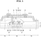
- FIG. 1 is a schematic view illustrating an organic light-emitting display device according to a first embodiment of the present disclosure.
- the organic light-emitting display device includes a thin film transistor T located on a first substrate 10, which is defined by a light emission area E/A and a transmission area T/A, a passivation layer 13 provided on the thin film transistor T, a planarization film 14 provided on the passivation layer 13, a first electrode 51 located on a region of the planarization film 14 corresponding to the light emission area E/A, the first electrode 51 being electrically connected to the thin film transistor T, an organic light emissive layer 52 provided on the first electrode 51, and a second electrode 53 provided on the organic light emissive layer 52.
- a shielding layer 56 is provided on a region of the planarization film 14 corresponding to the transmission area T/A.
- a black bank 15 is further provided so as to correspond to a region between the transmission area T/A and the emission area E/A. The black bank 15 covers the edge of the first electrode 51.
- FIG. 1 A further detailed description will be given with reference to FIG. 1 .
- a buffer layer 11 is located on the first substrate 10.
- the buffer layer 11 serves to prevent moisture or impurities from permeating through the first substrate 10 and to planarize the upper part of the first substrate 10.
- the buffer layer 11 may be made of an inorganic insulation material, such as SiNx or SiOx.
- a gate insulation film 26 is located on the active layer 21, and a gate electrode 27 is located on the gate insulation film 26.
- the gate electrode 27 is located so as to overlap a channel region of the active layer 21 via the gate insulation film 26.
- the gate electrode 27 may have a single-layer or multi-layer structure made of any one selected from among molybdenum (Mo), aluminum (Al), chrome (Cr), gold (Au), titanium (Ti), nickel (Ni), neodymium (Nd), and copper (Cu) or an alloy thereof.
- a shading layer 8 is located under a region in which the thin film transistor T is located.
- the shading layer 8 may serve to block light incident on the active layer 21 and to reduce parasitic capacitance generated between the thin film transistor T and various wires (not shown).
- the shading layer 8 may be made of any one selected from among silver (Ag), nickel (Ni), gold (Au), platinum (Pt), aluminum (Al), copper (Cu), molybdenum (Mo), titanium (Ti), and neodymium (Nd) or an alloy thereof.
- An interlayer insulation film 12 is located on the gate electrode 27.
- the interlayer insulation film 12 is located on the entirety of one surface of the first substrate 10 extending from an active area A/A so as to include a lower pad unit of a pad area.
- the interlayer insulation film 12 may be formed so as to have a single-layer or multi-layer structure made of an inorganic insulation material, such as SiNx or SiOx.
- the interlayer insulation film 12 is provided with a first contact hole HI, through which a source region 22 of the active layer 21 is exposed, and a second contact hole H2, through which a drain region 23 is exposed.
- a source electrode 24 is connected to the source region 22 through the first contact hole HI, and a drain electrode 25 is connected to the drain region 23 through the second contact hole H2.
- the source electrode 24 and the drain electrode 25 may have a single-layer or multi-layer structure made of any one selected from among molybdenum (Mo), aluminum (Al), chrome (Cr), gold (Au), titanium (Ti), nickel (Ni), neodymium (Nd), and copper (Cu) or an alloy thereof.
- the source electrode 24 may have a two-layer structure including a first source division layer 24a and a second source division layer 24b
- the drain electrode 25 may have a two-layer structure including a first drain division layer 25a and a second drain division layer 25b.
- the passivation layer 13 is located on the thin film transistor T.
- the passivation layer 13 may be formed so as to have a single-layer or multi-layer structure made of an inorganic film, such as SiNx or SiOx.
- the passivation layer 13 serves to protect the thin film transistor T. Depending on the design, the passivation layer 13 may be omitted.
- the planarization film 14 is located on the passivation layer 13.
- the planarization film 14 serves to planarize the upper part of the first substrate 10 on which the thin film transistor T is located.
- the planarization film 14 may be made of, for example, acrylic resin, epoxy resin, phenolic resin, polyamide resin, or polyimide resin.
- the first electrode 51 is formed on the planarization film 14.
- the first electrode 51 is provided on a position corresponding to the emission area E/A of the first substrate 10, and is electrically connected to the thin film transistor T.
- the first electrode 51 is electrically connected to a drain electrode 25 of the thin film transistor T through a third contact hole H3 formed by removing a portion of the planarization film 14 and the passivation layer 13 so as to expose the drain electrode 25.
- the first electrode 51 may serve as an anode or a cathode. In FIG. 1 , the first electrode 51 serves as an anode.
- the first electrode 51 is made of a transparent conductive material having a relatively large work function value, such as ITO, IZO, ZnO, or IGZO.
- the first electrode 51 may be configured so as to include a metal material exhibiting high reflectance, such as aluminum (Al), silver (Ag), or APC (Ag/Pb/Cu).
- a metal material exhibiting high reflectance such as aluminum (Al), silver (Ag), or APC (Ag/Pb/Cu).
- the first electrode 51 includes a first electrode lower-layer part 51a, a first electrode middle-layer part 51b, and a first electrode upper-layer part 51c.
- the middle-layer part 51b includes a material exhibiting high reflectance, such as silver (Ag), and the lower-layer part 51a and the upper-layer part 51c are made of a transparent conductive material in order to protect the metal layer of the middle-layer part 51b, which is highly reflective.
- the first electrode upper-layer part 51c is made of a transparent conductive material such that light reflected by the first electrode middle-layer part 51b is transmitted through the first electrode upper-layer part 51c and emitted to the upper side of the organic light-emitting element.
- the shielding layer 56 is provided on a position of the upper region of the planarization film 14 corresponding to the transmission area T/A.
- the shielding layer 56 may be made of a transparent conductive material that is separated from the first electrode 51 and is thus electrically isolated from the first electrode 51.
- the shielding layer 56 may be made of the same material as the first electrode lower-layer part 51a, and may be formed simultaneously with the first electrode lower-layer part 51a.
- the shielding layer 56 is provided so as to cover a portion of the upper region of the planarization film 14 corresponding to the transmission area T/A, and serves to prevent outgassing through the planarization film 14. In addition, the shielding layer 56 extends to the side surface of the planarization film 14 to prevent the planarization film 14 from being exposed to the outside.
- the black bank 15 is provided at a position of the upper region of the planarization film 14 corresponding to a region between the transmission area T/A and the emission area E/A.
- the black bank 15 is made of a material exhibiting a low dielectric constant.
- the black bank 15 may be made of at least one selected from among black resin, graphite powder, gravure ink, black spray, and black enamel, all of which are organic insulation materials.
- the black bank 15 serves to define a pixel region of the organic light-emitting display device and to absorb light incident from outside, thereby preventing the reflection of the external light.
- the black bank 15 covers a region of the upper layer of the planarization film 14 where the shielding layer 56 is not provided to further prevent outgassing through the planarization film 14.
- the organic light emissive layer 52 is provided on the first electrode 51.
- the organic light emissive layer 52 may be configured as a series of layers, some of which might not, as individual layers emit light, but the structure of layer 52 as a whole is a light emissive layer.
- the layer 52 may have a structure including a hole injection layer (HIL)/a hole transport layer (HTL)/an light emissive layer (EML)/an electron transport layer (ETL)/an electron injection layer (EIL).
- the organic light emissive layer 52 may further include at least one functional layer for improving the light emission efficiency and lifespan of the emissive layer, such as a charge generation layer for generating charges, an additional electron transport layer, or an additional hole transport layer.
- the organic light emissive layer 52 may extend so as to cover the upper part of the black bank 15 for mask reduction.
- the light emissive layer of the organic light emissive layer 52 may be provided only on the first electrode 51.
- the second electrode 53 is provided so as to cover the organic light emissive layer 52 and the upper part of the black bank 15.
- the second electrode 53 serves as a cathode.
- the second electrode 53 is made of a metal material having a sufficiently small thickness (e.g., about 200 ⁇ or less) to transmit light and a small work function value such that light from the organic light emissive layer 52 is transmitted through the second electrode 53, thereby achieving top emission.
- the second electrode 53 may be made of at least one selected from among silver (Ag), titanium (Ti), aluminum (Al), molybdenum (Mo), and an alloy of silver (Ag) and magnesium (Mg).
- the second electrode 53 is made of a transparent conductive material, such as ITO, IZO, IGZO, or ZnO, such that light from the organic light emissive layer 52 is transmitted through the second electrode 53, thereby achieving top emission.
- a second substrate may be laminated to the second electrode 53 via an adhesive layer (not shown). Depending on the design, the adhesive layer and the second substrate may be omitted. The second substrate may be replaced by a thin film type encapsulation member.
- the organic light-emitting display device is a transparent organic light-emitting display device including a transmission area T/A and alight emission area E/A wherein no additional polarizing plate is provided.
- a transparent organic light-emitting display device of the related art does not include a polarizing plate, external light is reflected and is visible to a user when images are displayed. Consequently, the reflection of external light deteriorates the quality of the displayed images.
- the main region from which the external light is reflected is a region around the light emission area E/A in which circuits are located.
- the external light is reflected by metal constituting the circuits.
- the black bank 15 is provided between the transmission area T/A and the light emission area E/A.
- the black bank 15 is provided around the emission area E/A to absorb external light, thereby minimizing the reflection of the external light by the metal constituting the circuits. According to the present disclosure, therefore, the black bank 15 is provided around the emission area E/A, thereby minimizing the reflection of the external light. Since the black bank 15 is provided only around the emission area and the shielding layer is provided on the other regions, transmittance is improved while deterioration in quality of images due to the external light is minimized. Consequently, the organic light-emitting display device according to the present disclosure has the effect of realizing a transparent display having excellent image quality.
- FIG. 2 is a schematic view illustrating an organic light-emitting display device including an auxiliary electrode and a connection electrode according to a second embodiment of the present disclosure.
- the organic light-emitting display device includes a thin film transistor T located on a first substrate 10, which is defined by an emission area E/A, a transmission area T/A, an auxiliary electrode area Aux/A, a passivation layer 13 provided on the thin film transistor T, a first planarization film 14a provided on the passivation layer 13, a connection electrode 41 located on the first planarization film 14a so as to contact the thin film transistor T, a second planarization film 14b for covering the connection electrode 41, a first electrode 51 located on a region of the second planarization film 14b corresponding to the emission area E/A, the first electrode 51 being electrically connected to the thin film transistor T, an organic light emissive layer 52 provided on the first electrode 51, and a second electrode 53 provided on the organic light emissive layer 52.
- the auxiliary electrode 30 is provided on the auxiliary electrode area Aux/A.
- the auxiliary electrode 30 may include a first auxiliary electrode 31 located on the same layer as the connection electrode 41 and a second auxiliary electrode 32 located on the same layer as the first electrode 51.
- the second electrode 53 is made of a transparent conductive material for top emission or a sufficiently thin metal material to transmit light, whereby the second electrode 53 has high resistance.
- the auxiliary electrode 30 is connected to the second electrode 53 to reduce the resistance of the second electrode 53.
- a first shielding layer 56a may be further provided on a region of the first planarization film 14a corresponding to the transmission area T/A.
- the first shielding layer 56a serves to prevent outgassing through the first planarization film 14a.
- the first shielding layer 56a is made of a transparent conductive material to transmit external light.
- the first shielding layer 56a extends to the side surface of the first planarization film 14a to cover the side surface of the first planarization film 14a.
- a second shielding layer 56b is further provided on a region of the second planarization film 14b corresponding to the transmission area T/A.
- the second shielding layer 56b serves to prevent outgassing through the second planarization film 14b.
- the second shielding layer 56b is made of a transparent conductive material, like the first shielding layer 56a.
- the second shielding layer 56b extends to the side surface of the second planarization film 14b to cover the side surface of the second planarization film 14b.
- a black bank 15 is further provided on a region of the second planarization film 14b corresponding to a region between the transmission area T/A and the emission area E/A.
- the black bank 15 covers the edge of the first electrode 51.
- the black bank 15 may be further provided on a region of the second planarization film 14b corresponding to a region between the auxiliary electrode area Aux/A and the transmission area T/A.
- the black bank 15 may be made of at least one selected from among black resin, graphite powder, gravure ink, black spray, and black enamel, all of which are organic insulation materials.
- the black bank 15 serves to define a pixel region of the organic light-emitting display device and to absorb light incident from outside, thereby preventing the reflection of the external light.
- the black bank 15 covers a region of the upper layer of the second planarization film 14b where the second shielding layer 56b is not provided to further prevent outgassing through the second planarization film 14b.
- the thin film transistor T is provided on the first substrate 10.
- a shading layer 8 is located between the thin film transistor T and the first substrate 10.
- the thin film transistor T and the shading layer 8 are the same as those described in the first embodiment, and therefore a detailed description thereof will be omitted.
- the passivation layer 13 is provided on the thin film transistor T.
- the first planarization film 14a is provided on the passivation layer 13.
- the first planarization film 14a has the same characteristics as the planarization film 14 of the first embodiment.
- the first planarization film 14a is provided with a third contact hole H3 formed by removing a portion of the first planarization film 14a and the passivation layer 13 so as to expose a drain electrode 25.
- connection electrode 41 is provided on a position of the first planarization film 14a corresponding to the emission area E/A.
- the second planarization film 14b is further provided due to the further provision of the first auxiliary electrode 31.
- the connection electrode 41 is further provided to connect the first electrode 51 and the drain electrode 25 on the first planarization film 14a.
- the connection electrode 41 may be formed to have a three-layer structure including a lower-layer part 41a, a middle-layer part 41b, and an upper-layer part 41c.
- the middle-layer part 41b of the connection electrode 41 may be made of a material exhibiting high conductivity, such as aluminum (Al), chrome (Cr), or copper (Cu).
- the above materials exhibit high electrical conductivity, but have low resistance to external oxygen or moisture.
- the lower-layer part 41a and the upper-layer part 41c of the connection electrode 41 may be made of a material exhibiting high corrosion resistance to protect the middle-layer part 41b of the connection electrode 41.
- the lower-layer part 41a of the connection electrode 41 is made of MoTi.
- the lower-layer part 41a of the connection electrode 41 may also be made of a transparent conductive material.
- the lower-layer part 41a of the connection electrode 41 may be made of various other materials.
- the upper-layer part 41c of the connection electrode 41 is made of a transparent conductive material, such as ITO, IZO, IGZO, or ZnO, to protect the middle-layer part 41b of the connection electrode 41.
- the second planarization film 14b is provided on the connection electrode 41.
- the second planarization film 14b covers the irregularities formed by the connection electrode 41 and the auxiliary electrode 30, whereby the upper surface of the second planarization film 14b is planarized.
- the second planarization film 14b may be made of the same material as the first planarization film 14a.
- the first electrode 51 is located on a region of the second planarization film 14b corresponding to the light emission area E/A.
- the organic light emissive layer 52 is provided on the first electrode 51, and the second electrode 53 is provided on the organic light emissive layer 52.
- the first electrode 51 includes a lower-layer part 51a, a middle-layer part 51b, and an upper-layer part 51c.
- the middle-layer part 51b of the first electrode 51 includes a material exhibiting high reflectance, such as silver (Ag), and the lower-layer part 51a and the upper-layer part 51c of the first electrode 51 are made of a transparent conductive material in order to protect the metal layer of the middle-layer part 51b of the first electrode 51, which is highly reflective.
- the first electrode 51 is electrically connected to the connection electrode 41 via a fourth contact hole H4 provided on the second planarization film 14b.
- the organic light emissive layer 52 and the second electrode 53 are the same as those described in the first embodiment, and therefore a detailed description thereof will be omitted.
- a portion of the transmission area T/A of the first substrate 10 is defined as the auxiliary electrode area Aux/A.
- the auxiliary electrode 30 is provided on the auxiliary electrode area Aux/A. As previously described, the auxiliary electrode 30 includes the first and second auxiliary electrodes 31 and 32.
- the first auxiliary electrode 31 is formed on the same layer as the connection electrode 41.
- the first auxiliary electrode 31 may have a three-layer structure including a first layer 31a, a second layer 31b, and a third layer 31c.
- the second layer 31b of the first auxiliary electrode 31 may be made of a material exhibiting high conductivity, such as aluminum (Al), chrome (Cr), or copper (Cu), like the middle-layer part 41b of the connection electrode 41.
- the first layer 31a and the third layer 31c of the first auxiliary electrode 31 may be made of a material exhibiting high corrosion resistance to protect the second layer 31b of the first auxiliary electrode 31.
- the first layer 31a of the first auxiliary electrode 31 is made of MoTi.
- the first 31a of the first auxiliary electrode 31 may also be made of a transparent conductive material.
- the first layer 31a of the first auxiliary electrode 31 may be made of various other materials.
- the third layer 31c of the first auxiliary electrode 31 is made of a transparent conductive material, such as ITO, IZO, IGZO, or ZnO, to protect the second layer 31b of the first auxiliary electrode 31.
- the second auxiliary electrode 32 is formed on the same layer as the first electrode 51. That is, the second auxiliary electrode 32 is located on the second planarization film 14b. The second auxiliary electrode 32 is electrically connected to the first auxiliary electrode 31 via a fifth contact hole H5 provided on the second planarization film 14b for allowing the third layer 31c of the first auxiliary electrode 31 to be exposed therethrough.
- the second auxiliary electrode 32 may have a three-layer structure including a fourth layer 32a, a fifth layer 32b, and a sixth layer 32c.
- the fifth layer 32b of the second auxiliary electrode 32 includes a material exhibiting high reflectance, such as silver (Ag), and the fourth layer 32a and the sixth layer 32c of the second auxiliary electrode 32 are made of a transparent conductive material, such as ITO, IZO, IGZO, or ZnO, to protect the highly reflective material of the fifth layer 32b of the second auxiliary electrode 32.
- the second auxiliary electrode 32 may be made of the same material as the first electrode 51.
- a partition wall 54 made of an organic insulation material and having a reverse taper shape may be further provided on the second auxiliary electrode 32. Since opposite side surfaces of the partition wall 54 have a reverse taper shape, a portion of the organic light emissive layer 52 may be discontinuous at the upper side of the partition wall 54. However, the organic light emissive layer 52 is not formed around the partition wall 54. As a result, the sixth auxiliary electrode division layer 32c of the second auxiliary electrode 32 is exposed around the partition wall 54, whereby the second electrode 53 and the second auxiliary electrode 32 contact each other around the partition wall 54.
- the first shielding layer 56a is provided on a region of the first planarization film 14a corresponding to the transmission area T/A.
- the second shielding layer 56b is provided on a region of the second planarization film 14b corresponding to the transmission area T/A.
- the first shielding layer 56a covers the upper part of the first planarization film 14a to prevent outgassing through the first planarization film 14a such that the organic light emissive layer 52 of the emission area E/A is not affected
- the second shielding layer 56b covers the upper part of the second planarization film 14b to prevent outgassing through the second planarization film 14b such that the organic light emissive layer 52 is not affected.
- the first and second shielding layers 56a and 56b may be made of the previously described transparent conductive material.
- the third layer 31c of the first auxiliary electrode 31 may be made of a transparent conductive material to protect the second layer 31b of the first auxiliary electrode 31.
- the first shielding layer 56a may be integrally formed with the third layer 31c of the first auxiliary electrode 31.
- the first shielding layer 56a and the third layer 31c of the first auxiliary electrode 31 may be integrally formed so as to be electrically connected to each other.
- the fifth division layer 32b of the second auxiliary electrode 32 is made of a metal material exhibiting high reflectance, and the fourth and sixth layers 32a and 32c of the second auxiliary electrode 32 are made of a transparent conductive material to protect the metal material.
- the second shielding layer 56b may be integrally formed with the fourth layer 32a of the second auxiliary electrode 32.
- the fourth layer 32a of the second auxiliary electrode 32 and the second shielding layer 56b may be integrally formed so as to be electrically connected to each other.
- the first shielding layer 56a is connected to the third division layer 31c of the first auxiliary electrode 31, and the second shielding layer 56b is connected to the sixth layer 32c of the second auxiliary electrode 32.
- the first shielding layer 56a and the second shielding layer 56b are electrically isolated from the first electrode 51 and the connection electrode 41. That is, the first shielding layer 56a and the second shielding layer 56b may be connected to the auxiliary electrode 30 so as to perform some of the roles of the auxiliary electrode 30. Consequently, the organic light-emitting display device according to the present disclosure has substantially the same effect as increasing the area of the auxiliary electrode 30, thereby compensating for the low resistance of the second electrode 53.
- first shielding layer 56a and the second shielding layer 56b may be connected to each other at the side surface C of the boundary line between the first planarization film 14a and the second planarization film 14b.
- first shielding layer 56a and the second shielding layer 56b may substantially serve as the auxiliary electrode.
- the black bank 15 is provided on a region of the second planarization film 14b corresponding to a region between the transmission area T/A and the emission area E/A, like the first embodiment.
- the black bank 15 is made of the same material as in the first embodiment to cover a region on the second planarization film 14b where the shielding layer 56 is not provided, thereby further preventing outgassing through the second planarization film 14b.
- the black bank 15 may be further provided on a region of the second planarization film 14b corresponding to a region between the auxiliary electrode area Aux/A and the transmission area T/A.
- the second auxiliary electrode 32 in the auxiliary electrode area Aux/A also includes a metal exhibiting high reflectance. Consequently, a region on which the auxiliary electrode 30 is formed is one of the sections where there is a high possibility of external light being reflected.
- the black bank 15 covers the edge of the second auxiliary electrode 32 to prevent upward outgassing through the second planarization film 14b and to reduce the reflection of external light due to the second auxiliary electrode 32.
- a second substrate may be laminated to the second electrode 53 via an adhesive layer (not shown).
- the adhesive layer and the second substrate may be omitted.
- the second substrate may be replaced by a thin film type encapsulation member.
- FIGs. 3A to 3G are views illustrating the method of manufacturing the organic light-emitting display device according to the second embodiment of the present disclosure.
- a shading layer 8 is formed on a first substrate 10, and then a buffer layer 11 is formed on the entirety of one surface of the first substrate 10 by deposition so as to cover the upper part of the shading layer 8.
- the shading layer 8 may be formed by depositing and patterning any one selected from among silver (Ag), nickel (Ni), gold (Au), platinum (Pt), aluminum (Al), copper (Cu), molybdenum (Mo), titanium (Ti), and neodymium (Nd) or an alloy thereof.
- the buffer layer 11 is formed by depositing an inorganic insulation material.
- an active layer 21 made of a semiconductor material is formed on the buffer layer 11.
- a gate insulation film 26 and a gate electrode 27 are sequentially formed on a channel region of the active layer 21.
- the gate electrode 27 may be formed by depositing and patterning a second metal layer (not shown) having a single-layer or multi-layer structure made of any one selected from among molybdenum (Mo), aluminum (Al), chrome (Cr), gold (Au), titanium (Ti), nickel (Ni), neodymium (Nd), and copper (Cu) or an alloy thereof.
- Mo molybdenum
- Al aluminum
- Cr chrome
- Au gold
- Ti titanium
- Ni nickel
- Nd neodymium
- Cu copper
- the disclosure is not limited thereto.
- the active layer 21 is doped with a dopant using the gate electrode 27 as a mask to form a source region 22 and a drain region 23.
- the active layer 21 is made of an oxide semiconductor
- opposite sides of the active layer 21 may be made conductive through plasma processing to form source and drain regions 22 and 23.
- an interlayer insulation film 12 is formed on the entire surface of the first substrate 10, including the gate electrode 27 and a lower pad unit.
- the interlayer insulation film 12 may be made of an inorganic insulation material, like the buffer layer 11.
- the interlayer insulation film 12 is patterned to form a first contact hole HI, through which the source region 22 is exposed, and a second contact hole H2, through which the drain region 23 is exposed.
- a source electrode 24 is formed on the interlayer insulation film 12 so as to be connected to the source region 22 through the first contact hole HI, and a drain electrode 25 is formed so as to be connected to the drain region 23 through the second contact hole H2.
- the source electrode 24 and the drain electrode 25 may be formed so as to have a multi-layer structure.
- the source and drain electrodes 24 and 25 have a two-layer structure of MoTi/Cu
- two-layer metals of MoTi/Cu may be stacked and simultaneously patterned on the entire upper surface of the interlayer insulation film 12 to simultaneously form the source and drain electrodes 24 and 25.
- a first planarization film 14a is formed on a thin film transistor T.
- the first planarization film 14a may be made of acrylic resin, epoxy resin, phenolic resin, polyamide resin, or polyimide resin.
- a third contact hole H3 for allowing a connection electrode 41 to be connected to the drain electrode 25 therethrough is formed on the first planarization film 14a.
- a transparent conductive material such as ITO, is formed so as to cover the middle-layer part 41b of the connection electrode 41 and the second layer 31b of the first auxiliary electrode 31, and is patterned to form a upper-layer part 41c of the connection electrode 41, a first shielding layer 56a, and a third layer 31c of the first auxiliary electrode 31.
- a second planarization film 14b is formed so as to cover the connection electrode 41 and the first auxiliary electrode 31.
- the second planarization film 14b is provided with a fourth contact hole H4, through which the connection electrode 41 is exposed, and a fifth contact hole H5, through which a second auxiliary electrode 32 is exposed.
- a metal layer 410 from which a first electrode 51 and a second auxiliary electrode 32 will be formed, is formed on the second planarization film 14b so as to cover the fourth contact hole H4 and the fifth contact hole H5.
- the metal layer 410 may be formed so as to have a three-layer structure including a third metal layer 411, a fourth metal layer 412, and a fifth metal layer 413.
- the metal layer 410 may be formed so as to have a three-layer structure of ITO/Ag/ITO.
- a photoresist 80 is applied to the upper part of the metal layer 410, and is patterned using a half-tone mask to partially remove the portion of the photoresist 80 where a second shielding layer 56b will be located, to completely remove the portion of the photoresist 80 where a black bank 15 will be located, and to leave the portion of the photoresist 80 corresponding to an emission area E/A in a thick state.
- etching is performed to remove the portion of the metal layer 410 where a black bank 15 will be located.
- ashing is performed to remove the portion of the photoresist 80 where a second shielding layer 56b will be located and to leave the portion of the photoresist 80 corresponding to an emission area E/A.
- etching is performed again to form a first electrode 51, a second shielding layer 56b, and a second auxiliary electrode 32.
- a black bank 15 is formed so as to cover the edge of the first electrode 51 and the edge of the second auxiliary electrode 32, and a partition wall 54 is formed on the second auxiliary electrode 32.
- an organic light emissive layer 52 and a second electrode 53 are deposited on the first electrode 51.
- the organic light emissive layer 52 and the second electrode 53 may also be formed on the black bank 15 and the partition wall 54.
- the organic light emissive layer 52 is not formed around the partition wall 54, but the second electrode 53 is formed around the partition wall 54 such that the second electrode 53 and the second auxiliary electrode 32 are connected to each other around the partition wall 54.
- the black bank is provided between the transmission area and the emission area.
- the black bank is provided around the emission area to absorb external light, thereby minimizing the reflection of the external light by metal constituting the circuits.
- outgassing through the planarization film is prevented using the shielding layer in the transmission area, and the shielding layer is made of a transparent conductive material to transmit external light. According to the present disclosure, therefore, the black bank is provided around the emission area, thereby minimizing the reflection of the external light.
- the organic light-emitting display device has the effect of realizing a transparent display having excellent image quality.
Landscapes
- Engineering & Computer Science (AREA)
- Microelectronics & Electronic Packaging (AREA)
- Physics & Mathematics (AREA)
- Optics & Photonics (AREA)
- Geometry (AREA)
- Manufacturing & Machinery (AREA)
- Electroluminescent Light Sources (AREA)
Abstract
Description
- This application claims the benefit of Korean Patent Application No.
10-2016-0184484, filed on December 30, 2016 - The present disclosure relates to an organic light-emitting display device, and more particularly to an organic light-emitting display device that is capable of reducing the reflection of external light and improving transmittance when a transparent display is realized using the organic light-emitting display device.
- Image display devices, which are a core technology in the information and communication age and serve to display various kinds of information on a screen, have been developed such that the image display devices are thinner, lighter, and portable and exhibit high performance. In addition, organic light-emitting display devices, which control the amount of light that is emitted from an organic light-emitting layer to display an image, have been highlighted as flat panel display devices that have lower weight and volume than cathode ray tubes (CRT).
- In an organic light-emitting display device, a plurality of pixels is arranged in the form of a matrix to display images. Each pixel includes a light-emitting element, and the organic light-emitting display device includes a pixel-driving circuit including a plurality of transistors configured to independently drive the respective light-emitting elements and storage capacitors. Each light-emitting element includes an emission layer disposed between a first electrode and a second electrode.
- In recent years, research has been actively conducted into top-emission type organic light-emitting display devices that are capable of realizing a transparent display. In organic light-emitting display devices that realize such a transparent display, a polarizing plate for reducing the reflection of external light cannot be used. As a result, transparent top-emission type organic light-emitting display devices do not satisfactorily prevent the reflection of external light, which causes deterioration in the quality of images.
- Accordingly, the present disclosure is directed to an organic light-emitting display device that substantially obviates one or more problems due to limitations and disadvantages of the related art.
- An object of the present disclosure is to provide an organic light-emitting display device that is capable of preventing the reflection of light incident from outside and improving transparency when a transparent display is realized.
- Additional advantages, objects, and features of the disclosure will be set forth in part in the description which follows and in part will become apparent to those having ordinary skill in the art upon examination of the following, or may be learned from practice of the disclosure. The objectives and other advantages of the disclosure may be realized and attained by the structure particularly pointed out in the written description and claims hereof as well as the appended drawings.
- To achieve these objects and other advantages and in accordance with the purpose of the disclosure, as embodied and broadly described herein, an organic light-emitting display device includes a first substrate defined by a transmission area and a light emission area, a first electrode located on a region of a planarization film, which covers a thin film transistor, corresponding to the light emission area, the first electrode being electrically connected to the thin film transistor, and a shielding layer located to cover a region of the planarization film corresponding to the transmission area and the side surface of the planarization film, the shielding layer being electrically isolated from the first electrode. A black bank is provided between the transmission area and the light emission area so as to cover the edge of the first electrode, and an organic light emissive layer and a second electrode, which covers the organic light emissive layer, are sequentially formed on the first electrode.
- Various embodiments provide an organic light-emitting display device comprising: a first substrate having a transmission area and a light emission area; a thin film transistor provided on the first substrate; a planarization film located to cover the thin film transistor; a first electrode located on a region of the planarization film corresponding to the light emission area, the first electrode being electrically connected to the thin film transistor; a shielding layer located to cover a region of the planarization film corresponding to the transmission area and a side surface of the planarization film, the shielding layer being electrically isolated from the first electrode; a black bank located between the transmission area and the light emission area for covering an edge of the first electrode; an organic light emissive layer located on the first electrode; and a second electrode located to cover the organic light emissive layer.
- In one or more embodiments, the shielding layer is made of a transparent conductive material.
- In one or more embodiments, the first electrode comprises: a lower-layer part made of a transparent conductive material; a middle-layer part comprising at least one selected from among aluminum (Al), silver (Ag), and APC (Ag/Pb/Cu); and an upper-layer part made of the transparent conductive material.
- In one or more embodiments, the shielding layer is made of a same material as the first electrode lower-layer part and is formed in a same layer as the first electrode lower-layer part.
- Various embodiments provide an organic light-emitting display device comprising: a first substrate having a transmission area and a light emission area; a thin film transistor provided on the first substrate; a first planarization film located to cover the thin film transistor; a connection electrode located on a region of the first planarization film corresponding to the light emission area, the connection electrode being electrically connected to the thin film transistor; a first shielding layer located on a region of the first planarization film corresponding to the transmission area, the first shielding layer being electrically isolated from the connection electrode, the first shielding layer extending to a side surface of the first planarization film so as to cover the side surface of the first planarization film; a second planarization film located to cover the connection electrode and the first shielding layer; a first electrode located on a region of the second planarization film corresponding to the light emission area, the first electrode being electrically connected to the connection electrode; a second shielding layer located on a region of the second planarization film corresponding to the transmission area, the second shielding layer being electrically isolated from the first electrode, the second shielding layer extending to a side surface of the second planarization film so as to cover the side surface of the second planarization film; a black bank located to cover an edge of the first electrode; an organic light emissive layer located on the first electrode; and a second electrode located on the organic light emissive layer.
- In one or more embodiments, a portion of the transmission area of the first substrate is defined as an auxiliary electrode area, and the organic light-emitting display device further comprises: a first auxiliary electrode provided on a portion of a region of the first planarization film corresponding to the auxiliary electrode area; and a second auxiliary electrode located on the second planarization film so as to overlap the first auxiliary electrode, the second auxiliary electrode being electrically connected to the first auxiliary electrode.
- In one or more embodiments, the organic light-emitting display device further comprises a black bank located to cover an edge of the second auxiliary electrode.
- In one or more embodiments, the first auxiliary electrode has a three-layer structure comprising a first layer, a second layer, and a third layer, the third layer being made of a transparent conductive material, the third layer being integrally formed with the first shielding layer.
- In one or more embodiments, the second auxiliary electrode has a three-layer structure comprising a fourth layer, a fifth layer, and a sixth layer, the fourth and sixth layers being made of a transparent conductive material, the fourth layer being integrally formed with the second shielding layer.
- In one or more embodiments, the first shielding layer and the second shielding layer contact each other at a side surface of the first planarization film.
- It is to be understood that both the foregoing general description and the following detailed description of the present disclosure are exemplary and explanatory and are intended to provide further explanation of the disclosure as claimed.
- The accompanying drawings, which are included to provide a further understanding of the disclosure and are incorporated in and constitute a part of this application, illustrate embodiment(s) of the disclosure and together with the description serve to explain the principle of the disclosure. In the drawings:
-
FIG. 1 is a schematic view illustrating an organic light-emitting display device according to a first embodiment of the present disclosure; -
FIG. 2 is a schematic view illustrating an organic light-emitting display device including an auxiliary electrode and a connection electrode according to a second embodiment of the present disclosure; and -
FIGs. 3A to 3G are views illustrating a method of manufacturing the organic light-emitting display device according to the second embodiment of the present disclosure. - Reference will now be made in detail to the preferred embodiments of the present disclosure, examples of which are illustrated in the accompanying drawings. Wherever possible, the same reference numbers will be used throughout the drawings to refer to the same or like parts. In the following description of the present disclosure, a detailed description of known functions and configurations incorporated herein will be omitted when it may obscure the subject matter of the present disclosure. In addition, the terms used in the following description are selected in consideration of ease of preparation of the specification, and may be different from the names of parts constituting an actual product.
- It will be understood that when an element is referred to as being "on," "above," "under" or "beside" another element, one or more intervening elements may be present therebetween, as long as the term "immediately" or "directly" is not used.
- It may be understood that, although the terms "first," "second," etc., may be used herein to describe various elements, these elements are not to be limited by these terms. These terms are generally only used to distinguish one element from another. In the following description, therefore, an element identified by "first" may be an element identified by "second" without falling outside the technical concept of the present disclosure.
- The size and thickness of each element shown in the drawings are given merely for the convenience of description, and the present disclosure is not limited thereto.
- Hereinafter, various embodiments of the present disclosure will be described in detail with reference to the accompanying drawings.
-
FIG. 1 is a schematic view illustrating an organic light-emitting display device according to a first embodiment of the present disclosure. - The organic light-emitting display device according to the first embodiment of the present disclosure includes a thin film transistor T located on a
first substrate 10, which is defined by a light emission area E/A and a transmission area T/A, apassivation layer 13 provided on the thin film transistor T, aplanarization film 14 provided on thepassivation layer 13, afirst electrode 51 located on a region of theplanarization film 14 corresponding to the light emission area E/A, thefirst electrode 51 being electrically connected to the thin film transistor T, an organic lightemissive layer 52 provided on thefirst electrode 51, and asecond electrode 53 provided on the organic lightemissive layer 52. Ashielding layer 56 is provided on a region of theplanarization film 14 corresponding to the transmission area T/A. Ablack bank 15 is further provided so as to correspond to a region between the transmission area T/A and the emission area E/A. Theblack bank 15 covers the edge of thefirst electrode 51. - A further detailed description will be given with reference to
FIG. 1 . - Referring to
FIG. 1 , abuffer layer 11 is located on thefirst substrate 10. Thebuffer layer 11 serves to prevent moisture or impurities from permeating through thefirst substrate 10 and to planarize the upper part of thefirst substrate 10. Thebuffer layer 11 may be made of an inorganic insulation material, such as SiNx or SiOx. - An
active layer 21 made of a semiconductor, such as a silicon or oxide semiconductor, is formed on thebuffer layer 11. Agate insulation film 26 is located on theactive layer 21, and agate electrode 27 is located on thegate insulation film 26. Thegate electrode 27 is located so as to overlap a channel region of theactive layer 21 via thegate insulation film 26. Thegate electrode 27 may have a single-layer or multi-layer structure made of any one selected from among molybdenum (Mo), aluminum (Al), chrome (Cr), gold (Au), titanium (Ti), nickel (Ni), neodymium (Nd), and copper (Cu) or an alloy thereof. - A
shading layer 8 is located under a region in which the thin film transistor T is located. Theshading layer 8 may serve to block light incident on theactive layer 21 and to reduce parasitic capacitance generated between the thin film transistor T and various wires (not shown). Theshading layer 8 may be made of any one selected from among silver (Ag), nickel (Ni), gold (Au), platinum (Pt), aluminum (Al), copper (Cu), molybdenum (Mo), titanium (Ti), and neodymium (Nd) or an alloy thereof. - An
interlayer insulation film 12 is located on thegate electrode 27. Theinterlayer insulation film 12 is located on the entirety of one surface of thefirst substrate 10 extending from an active area A/A so as to include a lower pad unit of a pad area. Theinterlayer insulation film 12 may be formed so as to have a single-layer or multi-layer structure made of an inorganic insulation material, such as SiNx or SiOx. - The
interlayer insulation film 12 is provided with a first contact hole HI, through which asource region 22 of theactive layer 21 is exposed, and a second contact hole H2, through which adrain region 23 is exposed. - A
source electrode 24 is connected to thesource region 22 through the first contact hole HI, and adrain electrode 25 is connected to thedrain region 23 through the second contact hole H2. Thesource electrode 24 and thedrain electrode 25 may have a single-layer or multi-layer structure made of any one selected from among molybdenum (Mo), aluminum (Al), chrome (Cr), gold (Au), titanium (Ti), nickel (Ni), neodymium (Nd), and copper (Cu) or an alloy thereof. As shown inFIG. 1 , thesource electrode 24 may have a two-layer structure including a firstsource division layer 24a and a secondsource division layer 24b, and thedrain electrode 25 may have a two-layer structure including a firstdrain division layer 25a and a seconddrain division layer 25b. - The
passivation layer 13 is located on the thin film transistor T. Thepassivation layer 13 may be formed so as to have a single-layer or multi-layer structure made of an inorganic film, such as SiNx or SiOx. Thepassivation layer 13 serves to protect the thin film transistor T. Depending on the design, thepassivation layer 13 may be omitted. - The
planarization film 14 is located on thepassivation layer 13. Theplanarization film 14 serves to planarize the upper part of thefirst substrate 10 on which the thin film transistor T is located. Theplanarization film 14 may be made of, for example, acrylic resin, epoxy resin, phenolic resin, polyamide resin, or polyimide resin. - The
first electrode 51 is formed on theplanarization film 14. Thefirst electrode 51 is provided on a position corresponding to the emission area E/A of thefirst substrate 10, and is electrically connected to the thin film transistor T. Thefirst electrode 51 is electrically connected to adrain electrode 25 of the thin film transistor T through a third contact hole H3 formed by removing a portion of theplanarization film 14 and thepassivation layer 13 so as to expose thedrain electrode 25. - The
first electrode 51 may serve as an anode or a cathode. InFIG. 1 , thefirst electrode 51 serves as an anode. - The
first electrode 51 is made of a transparent conductive material having a relatively large work function value, such as ITO, IZO, ZnO, or IGZO. In addition, thefirst electrode 51 may be configured so as to include a metal material exhibiting high reflectance, such as aluminum (Al), silver (Ag), or APC (Ag/Pb/Cu). The reason for this is that, in order to improve the efficiency of top emission and lifespan of the light-emitting element, light incident on the lower side of the organic light-emitting element is reflected upward, thereby contributing to the emission of the light-emitting element. A metal material exhibiting high reflectance, such as aluminum (Al) or silver (Ag), has low resistance to oxidization due to external oxygen or moisture. For this reason, thefirst electrode 51 includes a first electrode lower-layer part 51a, a first electrode middle-layer part 51b, and a first electrode upper-layer part 51c. The middle-layer part 51b includes a material exhibiting high reflectance, such as silver (Ag), and the lower-layer part 51a and the upper-layer part 51c are made of a transparent conductive material in order to protect the metal layer of the middle-layer part 51b, which is highly reflective. The first electrode upper-layer part 51c is made of a transparent conductive material such that light reflected by the first electrode middle-layer part 51b is transmitted through the first electrode upper-layer part 51c and emitted to the upper side of the organic light-emitting element. In the organic light-emitting display device according to the present disclosure, therefore, light incident on the lower side of the organic light-emitting element is reflected upward to contribute to the emission of the organic light-emitting element, thereby improving the efficiency and lifespan of the organic light-emitting element. - The
shielding layer 56 is provided on a position of the upper region of theplanarization film 14 corresponding to the transmission area T/A. Theshielding layer 56 may be made of a transparent conductive material that is separated from thefirst electrode 51 and is thus electrically isolated from thefirst electrode 51. Theshielding layer 56 may be made of the same material as the first electrode lower-layer part 51a, and may be formed simultaneously with the first electrode lower-layer part 51a. - The
shielding layer 56 is provided so as to cover a portion of the upper region of theplanarization film 14 corresponding to the transmission area T/A, and serves to prevent outgassing through theplanarization film 14. In addition, theshielding layer 56 extends to the side surface of theplanarization film 14 to prevent theplanarization film 14 from being exposed to the outside. - The
black bank 15 is provided at a position of the upper region of theplanarization film 14 corresponding to a region between the transmission area T/A and the emission area E/A. Theblack bank 15 is made of a material exhibiting a low dielectric constant. For example, theblack bank 15 may be made of at least one selected from among black resin, graphite powder, gravure ink, black spray, and black enamel, all of which are organic insulation materials. Theblack bank 15 serves to define a pixel region of the organic light-emitting display device and to absorb light incident from outside, thereby preventing the reflection of the external light. In addition, theblack bank 15 covers a region of the upper layer of theplanarization film 14 where theshielding layer 56 is not provided to further prevent outgassing through theplanarization film 14. - The organic light
emissive layer 52 is provided on thefirst electrode 51. The organic lightemissive layer 52 may be configured as a series of layers, some of which might not, as individual layers emit light, but the structure oflayer 52 as a whole is a light emissive layer. For example, thelayer 52 may have a structure including a hole injection layer (HIL)/a hole transport layer (HTL)/an light emissive layer (EML)/an electron transport layer (ETL)/an electron injection layer (EIL). In addition, the organic lightemissive layer 52 may further include at least one functional layer for improving the light emission efficiency and lifespan of the emissive layer, such as a charge generation layer for generating charges, an additional electron transport layer, or an additional hole transport layer. - The organic light
emissive layer 52 may extend so as to cover the upper part of theblack bank 15 for mask reduction. The light emissive layer of the organic lightemissive layer 52 may be provided only on thefirst electrode 51. - The
second electrode 53 is provided so as to cover the organic lightemissive layer 52 and the upper part of theblack bank 15. In the case in which thefirst electrode 51 serves as an anode, thesecond electrode 53 serves as a cathode. In a top-emission type organic light-emitting display device, thesecond electrode 53 is made of a metal material having a sufficiently small thickness (e.g., about 200Å or less) to transmit light and a small work function value such that light from the organic lightemissive layer 52 is transmitted through thesecond electrode 53, thereby achieving top emission. Thesecond electrode 53 may be made of at least one selected from among silver (Ag), titanium (Ti), aluminum (Al), molybdenum (Mo), and an alloy of silver (Ag) and magnesium (Mg). In addition, thesecond electrode 53 is made of a transparent conductive material, such as ITO, IZO, IGZO, or ZnO, such that light from the organic lightemissive layer 52 is transmitted through thesecond electrode 53, thereby achieving top emission. - A second substrate (not shown) may be laminated to the
second electrode 53 via an adhesive layer (not shown). Depending on the design, the adhesive layer and the second substrate may be omitted. The second substrate may be replaced by a thin film type encapsulation member. - The organic light-emitting display device according to the present disclosure is a transparent organic light-emitting display device including a transmission area T/A and alight emission area E/A wherein no additional polarizing plate is provided.
- Since a transparent organic light-emitting display device of the related art does not include a polarizing plate, external light is reflected and is visible to a user when images are displayed. Consequently, the reflection of external light deteriorates the quality of the displayed images.
- The main region from which the external light is reflected is a region around the light emission area E/A in which circuits are located. The external light is reflected by metal constituting the circuits.
- In the organic light-emitting display device according to the present disclosure, the
black bank 15 is provided between the transmission area T/A and the light emission area E/A. In the organic light-emitting display device according to the present disclosure, theblack bank 15 is provided around the emission area E/A to absorb external light, thereby minimizing the reflection of the external light by the metal constituting the circuits. According to the present disclosure, therefore, theblack bank 15 is provided around the emission area E/A, thereby minimizing the reflection of the external light. Since theblack bank 15 is provided only around the emission area and the shielding layer is provided on the other regions, transmittance is improved while deterioration in quality of images due to the external light is minimized. Consequently, the organic light-emitting display device according to the present disclosure has the effect of realizing a transparent display having excellent image quality. -
FIG. 2 is a schematic view illustrating an organic light-emitting display device including an auxiliary electrode and a connection electrode according to a second embodiment of the present disclosure. - The organic light-emitting display device according to the second embodiment includes a thin film transistor T located on a
first substrate 10, which is defined by an emission area E/A, a transmission area T/A, an auxiliary electrode area Aux/A, apassivation layer 13 provided on the thin film transistor T, afirst planarization film 14a provided on thepassivation layer 13, aconnection electrode 41 located on thefirst planarization film 14a so as to contact the thin film transistor T, asecond planarization film 14b for covering theconnection electrode 41, afirst electrode 51 located on a region of thesecond planarization film 14b corresponding to the emission area E/A, thefirst electrode 51 being electrically connected to the thin film transistor T, an organic lightemissive layer 52 provided on thefirst electrode 51, and asecond electrode 53 provided on the organic lightemissive layer 52. - An
auxiliary electrode 30 is provided on the auxiliary electrode area Aux/A. Theauxiliary electrode 30 may include a firstauxiliary electrode 31 located on the same layer as theconnection electrode 41 and a secondauxiliary electrode 32 located on the same layer as thefirst electrode 51. Thesecond electrode 53 is made of a transparent conductive material for top emission or a sufficiently thin metal material to transmit light, whereby thesecond electrode 53 has high resistance. Theauxiliary electrode 30 is connected to thesecond electrode 53 to reduce the resistance of thesecond electrode 53. - A
first shielding layer 56a may be further provided on a region of thefirst planarization film 14a corresponding to the transmission area T/A. Thefirst shielding layer 56a serves to prevent outgassing through thefirst planarization film 14a. Thefirst shielding layer 56a is made of a transparent conductive material to transmit external light. Thefirst shielding layer 56a extends to the side surface of thefirst planarization film 14a to cover the side surface of thefirst planarization film 14a. - A
second shielding layer 56b is further provided on a region of thesecond planarization film 14b corresponding to the transmission area T/A. Thesecond shielding layer 56b serves to prevent outgassing through thesecond planarization film 14b. Thesecond shielding layer 56b is made of a transparent conductive material, like thefirst shielding layer 56a. Thesecond shielding layer 56b extends to the side surface of thesecond planarization film 14b to cover the side surface of thesecond planarization film 14b. - A
black bank 15 is further provided on a region of thesecond planarization film 14b corresponding to a region between the transmission area T/A and the emission area E/A. Theblack bank 15 covers the edge of thefirst electrode 51. Theblack bank 15 may be further provided on a region of thesecond planarization film 14b corresponding to a region between the auxiliary electrode area Aux/A and the transmission area T/A. - As previously described, the
black bank 15 may be made of at least one selected from among black resin, graphite powder, gravure ink, black spray, and black enamel, all of which are organic insulation materials. Theblack bank 15 serves to define a pixel region of the organic light-emitting display device and to absorb light incident from outside, thereby preventing the reflection of the external light. In addition, theblack bank 15 covers a region of the upper layer of thesecond planarization film 14b where thesecond shielding layer 56b is not provided to further prevent outgassing through thesecond planarization film 14b. - A further detailed description will be given with reference to
FIG. 2 . - Referring to
FIG. 2 , the thin film transistor T is provided on thefirst substrate 10. Ashading layer 8 is located between the thin film transistor T and thefirst substrate 10. - The thin film transistor T and the
shading layer 8 are the same as those described in the first embodiment, and therefore a detailed description thereof will be omitted. Like the first embodiment, thepassivation layer 13 is provided on the thin film transistor T. - The
first planarization film 14a is provided on thepassivation layer 13. Thefirst planarization film 14a has the same characteristics as theplanarization film 14 of the first embodiment. Thefirst planarization film 14a is provided with a third contact hole H3 formed by removing a portion of thefirst planarization film 14a and thepassivation layer 13 so as to expose adrain electrode 25. - The
connection electrode 41 is provided on a position of thefirst planarization film 14a corresponding to the emission area E/A. - In the organic light-emitting display device according to the second embodiment of the present disclosure, the
second planarization film 14b is further provided due to the further provision of the firstauxiliary electrode 31. As a result, theconnection electrode 41 is further provided to connect thefirst electrode 51 and thedrain electrode 25 on thefirst planarization film 14a. Theconnection electrode 41 may be formed to have a three-layer structure including a lower-layer part 41a, a middle-layer part 41b, and an upper-layer part 41c. - The middle-
layer part 41b of theconnection electrode 41 may be made of a material exhibiting high conductivity, such as aluminum (Al), chrome (Cr), or copper (Cu). The above materials exhibit high electrical conductivity, but have low resistance to external oxygen or moisture. For this reason, the lower-layer part 41a and the upper-layer part 41c of theconnection electrode 41 may be made of a material exhibiting high corrosion resistance to protect the middle-layer part 41b of theconnection electrode 41. - Typically, the lower-
layer part 41a of theconnection electrode 41 is made of MoTi. The lower-layer part 41a of theconnection electrode 41 may also be made of a transparent conductive material. In addition, the lower-layer part 41a of theconnection electrode 41 may be made of various other materials. The upper-layer part 41c of theconnection electrode 41 is made of a transparent conductive material, such as ITO, IZO, IGZO, or ZnO, to protect the middle-layer part 41b of theconnection electrode 41. - The
second planarization film 14b is provided on theconnection electrode 41. Thesecond planarization film 14b covers the irregularities formed by theconnection electrode 41 and theauxiliary electrode 30, whereby the upper surface of thesecond planarization film 14b is planarized. Thesecond planarization film 14b may be made of the same material as thefirst planarization film 14a. - The
first electrode 51 is located on a region of thesecond planarization film 14b corresponding to the light emission area E/A. The organic lightemissive layer 52 is provided on thefirst electrode 51, and thesecond electrode 53 is provided on the organic lightemissive layer 52. - Like the first embodiment, the
first electrode 51 includes a lower-layer part 51a, a middle-layer part 51b, and an upper-layer part 51c. The middle-layer part 51b of thefirst electrode 51 includes a material exhibiting high reflectance, such as silver (Ag), and the lower-layer part 51a and the upper-layer part 51c of thefirst electrode 51 are made of a transparent conductive material in order to protect the metal layer of the middle-layer part 51b of thefirst electrode 51, which is highly reflective. Thefirst electrode 51 is electrically connected to theconnection electrode 41 via a fourth contact hole H4 provided on thesecond planarization film 14b. - The organic light
emissive layer 52 and thesecond electrode 53 are the same as those described in the first embodiment, and therefore a detailed description thereof will be omitted. - A portion of the transmission area T/A of the
first substrate 10 is defined as the auxiliary electrode area Aux/A. Theauxiliary electrode 30 is provided on the auxiliary electrode area Aux/A. As previously described, theauxiliary electrode 30 includes the first and secondauxiliary electrodes - The first
auxiliary electrode 31 is formed on the same layer as theconnection electrode 41. The firstauxiliary electrode 31 may have a three-layer structure including afirst layer 31a, asecond layer 31b, and athird layer 31c. - The
second layer 31b of the firstauxiliary electrode 31 may be made of a material exhibiting high conductivity, such as aluminum (Al), chrome (Cr), or copper (Cu), like the middle-layer part 41b of theconnection electrode 41. In addition, like theconnection electrode 41, thefirst layer 31a and thethird layer 31c of the firstauxiliary electrode 31 may be made of a material exhibiting high corrosion resistance to protect thesecond layer 31b of the firstauxiliary electrode 31. - Typically, the
first layer 31a of the firstauxiliary electrode 31 is made of MoTi. The first 31a of the firstauxiliary electrode 31 may also be made of a transparent conductive material. In addition, thefirst layer 31a of the firstauxiliary electrode 31 may be made of various other materials. Thethird layer 31c of the firstauxiliary electrode 31 is made of a transparent conductive material, such as ITO, IZO, IGZO, or ZnO, to protect thesecond layer 31b of the firstauxiliary electrode 31. - The second
auxiliary electrode 32 is formed on the same layer as thefirst electrode 51. That is, the secondauxiliary electrode 32 is located on thesecond planarization film 14b. The secondauxiliary electrode 32 is electrically connected to the firstauxiliary electrode 31 via a fifth contact hole H5 provided on thesecond planarization film 14b for allowing thethird layer 31c of the firstauxiliary electrode 31 to be exposed therethrough. - The second
auxiliary electrode 32 may have a three-layer structure including afourth layer 32a, afifth layer 32b, and asixth layer 32c. - Like the middle-
layer part 51b of thefirst electrode 51, thefifth layer 32b of the secondauxiliary electrode 32 includes a material exhibiting high reflectance, such as silver (Ag), and thefourth layer 32a and thesixth layer 32c of the secondauxiliary electrode 32 are made of a transparent conductive material, such as ITO, IZO, IGZO, or ZnO, to protect the highly reflective material of thefifth layer 32b of the secondauxiliary electrode 32. In other words, the secondauxiliary electrode 32 may be made of the same material as thefirst electrode 51. - A
partition wall 54 made of an organic insulation material and having a reverse taper shape may be further provided on the secondauxiliary electrode 32. Since opposite side surfaces of thepartition wall 54 have a reverse taper shape, a portion of the organic lightemissive layer 52 may be discontinuous at the upper side of thepartition wall 54. However, the organic lightemissive layer 52 is not formed around thepartition wall 54. As a result, the sixth auxiliaryelectrode division layer 32c of the secondauxiliary electrode 32 is exposed around thepartition wall 54, whereby thesecond electrode 53 and the secondauxiliary electrode 32 contact each other around thepartition wall 54. - The
first shielding layer 56a is provided on a region of thefirst planarization film 14a corresponding to the transmission area T/A. In addition, thesecond shielding layer 56b is provided on a region of thesecond planarization film 14b corresponding to the transmission area T/A. As previously described, thefirst shielding layer 56a covers the upper part of thefirst planarization film 14a to prevent outgassing through thefirst planarization film 14a such that the organic lightemissive layer 52 of the emission area E/A is not affected, and thesecond shielding layer 56b covers the upper part of thesecond planarization film 14b to prevent outgassing through thesecond planarization film 14b such that the organic lightemissive layer 52 is not affected. - The first and second shielding layers 56a and 56b may be made of the previously described transparent conductive material. In this case, the
third layer 31c of the firstauxiliary electrode 31 may be made of a transparent conductive material to protect thesecond layer 31b of the firstauxiliary electrode 31. Thefirst shielding layer 56a may be integrally formed with thethird layer 31c of the firstauxiliary electrode 31. In other words, thefirst shielding layer 56a and thethird layer 31c of the firstauxiliary electrode 31 may be integrally formed so as to be electrically connected to each other. - The
fifth division layer 32b of the secondauxiliary electrode 32 is made of a metal material exhibiting high reflectance, and the fourth andsixth layers auxiliary electrode 32 are made of a transparent conductive material to protect the metal material. Thesecond shielding layer 56b may be integrally formed with thefourth layer 32a of the secondauxiliary electrode 32. In other words, thefourth layer 32a of the secondauxiliary electrode 32 and thesecond shielding layer 56b may be integrally formed so as to be electrically connected to each other. - The
first shielding layer 56a is connected to thethird division layer 31c of the firstauxiliary electrode 31, and thesecond shielding layer 56b is connected to thesixth layer 32c of the secondauxiliary electrode 32. In addition, thefirst shielding layer 56a and thesecond shielding layer 56b are electrically isolated from thefirst electrode 51 and theconnection electrode 41. That is, thefirst shielding layer 56a and thesecond shielding layer 56b may be connected to theauxiliary electrode 30 so as to perform some of the roles of theauxiliary electrode 30. Consequently, the organic light-emitting display device according to the present disclosure has substantially the same effect as increasing the area of theauxiliary electrode 30, thereby compensating for the low resistance of thesecond electrode 53. - Meanwhile, the
first shielding layer 56a and thesecond shielding layer 56b may be connected to each other at the side surface C of the boundary line between thefirst planarization film 14a and thesecond planarization film 14b. As a result, thefirst shielding layer 56a and thesecond shielding layer 56b may substantially serve as the auxiliary electrode. - In the organic light-emitting display device according to the second embodiment of the present disclosure, the
black bank 15 is provided on a region of thesecond planarization film 14b corresponding to a region between the transmission area T/A and the emission area E/A, like the first embodiment. Theblack bank 15 is made of the same material as in the first embodiment to cover a region on thesecond planarization film 14b where theshielding layer 56 is not provided, thereby further preventing outgassing through thesecond planarization film 14b. - In addition, the
black bank 15 may be further provided on a region of thesecond planarization film 14b corresponding to a region between the auxiliary electrode area Aux/A and the transmission area T/A. The secondauxiliary electrode 32 in the auxiliary electrode area Aux/A also includes a metal exhibiting high reflectance. Consequently, a region on which theauxiliary electrode 30 is formed is one of the sections where there is a high possibility of external light being reflected. Theblack bank 15 covers the edge of the secondauxiliary electrode 32 to prevent upward outgassing through thesecond planarization film 14b and to reduce the reflection of external light due to the secondauxiliary electrode 32. - As previously described, a second substrate (not shown) may be laminated to the
second electrode 53 via an adhesive layer (not shown). Depending on the design, the adhesive layer and the second substrate may be omitted. The second substrate may be replaced by a thin film type encapsulation member. - Hereinafter, a method of manufacturing the organic light-emitting display device according to the present disclosure will be described with reference to the drawings. The method of manufacturing the organic light-emitting display device according to the first embodiment of the present disclosure and the method of manufacturing the organic light-emitting display device according to the second embodiment of the present disclosure are generally similar to each other. Consequently, the method of manufacturing the organic light-emitting display device according to the second embodiment of the present disclosure will be described, and the method of manufacturing the organic light-emitting display device according to the first embodiment of the present disclosure will be omitted.
-
FIGs. 3A to 3G are views illustrating the method of manufacturing the organic light-emitting display device according to the second embodiment of the present disclosure. - First, as shown in
FIG. 3A , ashading layer 8 is formed on afirst substrate 10, and then abuffer layer 11 is formed on the entirety of one surface of thefirst substrate 10 by deposition so as to cover the upper part of theshading layer 8. Theshading layer 8 may be formed by depositing and patterning any one selected from among silver (Ag), nickel (Ni), gold (Au), platinum (Pt), aluminum (Al), copper (Cu), molybdenum (Mo), titanium (Ti), and neodymium (Nd) or an alloy thereof. Thebuffer layer 11 is formed by depositing an inorganic insulation material. - Subsequently, as shown in
FIG. 3B , anactive layer 21 made of a semiconductor material is formed on thebuffer layer 11. Agate insulation film 26 and agate electrode 27 are sequentially formed on a channel region of theactive layer 21. - The
gate electrode 27 may be formed by depositing and patterning a second metal layer (not shown) having a single-layer or multi-layer structure made of any one selected from among molybdenum (Mo), aluminum (Al), chrome (Cr), gold (Au), titanium (Ti), nickel (Ni), neodymium (Nd), and copper (Cu) or an alloy thereof. However, the disclosure is not limited thereto. - Subsequently, the
active layer 21 is doped with a dopant using thegate electrode 27 as a mask to form asource region 22 and adrain region 23. In the case in which theactive layer 21 is made of an oxide semiconductor, opposite sides of theactive layer 21 may be made conductive through plasma processing to form source and drainregions - Subsequently, an
interlayer insulation film 12 is formed on the entire surface of thefirst substrate 10, including thegate electrode 27 and a lower pad unit. Theinterlayer insulation film 12 may be made of an inorganic insulation material, like thebuffer layer 11. - Subsequently, the
interlayer insulation film 12 is patterned to form a first contact hole HI, through which thesource region 22 is exposed, and a second contact hole H2, through which thedrain region 23 is exposed. - Subsequently, a
source electrode 24 is formed on theinterlayer insulation film 12 so as to be connected to thesource region 22 through the first contact hole HI, and adrain electrode 25 is formed so as to be connected to thedrain region 23 through the second contact hole H2. As previously described, thesource electrode 24 and thedrain electrode 25 may be formed so as to have a multi-layer structure. For example, when the source and drainelectrodes interlayer insulation film 12 to simultaneously form the source and drainelectrodes - Subsequently, as shown in
FIG. 3C , afirst planarization film 14a is formed on a thin film transistor T. Thefirst planarization film 14a may be made of acrylic resin, epoxy resin, phenolic resin, polyamide resin, or polyimide resin. A third contact hole H3 for allowing aconnection electrode 41 to be connected to thedrain electrode 25 therethrough is formed on thefirst planarization film 14a. - First and second metal layers 401 and 402, from which a
connection electrode 41 and a firstauxiliary electrode 31 will be formed, are deposited and patterned on thefirst planarization film 14a to form a lower-layer part 41a and a middle-layer part 41b of theconnection electrode 41, and afirst layer 31a and asecond layer 31b of the firstauxiliary electrode 31. - Subsequently, as shown in
FIG. 3D , a transparent conductive material, such as ITO, is formed so as to cover the middle-layer part 41b of theconnection electrode 41 and thesecond layer 31b of the firstauxiliary electrode 31, and is patterned to form a upper-layer part 41c of theconnection electrode 41, afirst shielding layer 56a, and athird layer 31c of the firstauxiliary electrode 31. - Subsequently, a
second planarization film 14b is formed so as to cover theconnection electrode 41 and the firstauxiliary electrode 31. Thesecond planarization film 14b is provided with a fourth contact hole H4, through which theconnection electrode 41 is exposed, and a fifth contact hole H5, through which a secondauxiliary electrode 32 is exposed. - Subsequently, as shown in
FIG. 3E , ametal layer 410, from which afirst electrode 51 and a secondauxiliary electrode 32 will be formed, is formed on thesecond planarization film 14b so as to cover the fourth contact hole H4 and the fifth contact hole H5. Themetal layer 410 may be formed so as to have a three-layer structure including athird metal layer 411, afourth metal layer 412, and afifth metal layer 413. For example, themetal layer 410 may be formed so as to have a three-layer structure of ITO/Ag/ITO. - Subsequently, a
photoresist 80 is applied to the upper part of themetal layer 410, and is patterned using a half-tone mask to partially remove the portion of thephotoresist 80 where asecond shielding layer 56b will be located, to completely remove the portion of thephotoresist 80 where ablack bank 15 will be located, and to leave the portion of thephotoresist 80 corresponding to an emission area E/A in a thick state. - Subsequently, as shown in
FIG. 3F , etching is performed to remove the portion of themetal layer 410 where ablack bank 15 will be located. Subsequently, ashing is performed to remove the portion of thephotoresist 80 where asecond shielding layer 56b will be located and to leave the portion of thephotoresist 80 corresponding to an emission area E/A. - Subsequently, etching is performed again to form a
first electrode 51, asecond shielding layer 56b, and a secondauxiliary electrode 32. Subsequently, ablack bank 15 is formed so as to cover the edge of thefirst electrode 51 and the edge of the secondauxiliary electrode 32, and apartition wall 54 is formed on the secondauxiliary electrode 32. - Subsequently, as shown in
FIG. 3G , an organic lightemissive layer 52 and asecond electrode 53 are deposited on thefirst electrode 51. At this time, the organic lightemissive layer 52 and thesecond electrode 53 may also be formed on theblack bank 15 and thepartition wall 54. The organic lightemissive layer 52 is not formed around thepartition wall 54, but thesecond electrode 53 is formed around thepartition wall 54 such that thesecond electrode 53 and the secondauxiliary electrode 32 are connected to each other around thepartition wall 54. - As is apparent from the above description, in the organic light-emitting display device according to the present disclosure, the black bank is provided between the transmission area and the emission area. In the organic light-emitting display device according to the present disclosure, the black bank is provided around the emission area to absorb external light, thereby minimizing the reflection of the external light by metal constituting the circuits. Additionally, in the organic light-emitting display device according to the present disclosure, outgassing through the planarization film is prevented using the shielding layer in the transmission area, and the shielding layer is made of a transparent conductive material to transmit external light. According to the present disclosure, therefore, the black bank is provided around the emission area, thereby minimizing the reflection of the external light. Since the black bank is provided only around the emission area and the shielding layer is provided on the other regions, transmittance is improved while deterioration in the quality of images due to external light is minimized. Consequently, the organic light-emitting display device according to the present disclosure has the effect of realizing a transparent display having excellent image quality.
- It will be apparent to those skilled in the art that various modifications and variations can be made in the present disclosure without departing from the scope of the disclosure. Thus, it is intended that the present disclosure covers the modifications and variations of this disclosure provided they come within the scope of the appended claims.
- The various embodiments described above can be combined to provide further embodiments.
- These and other changes can be made to the embodiments in light of the above-detailed description. In general, in the following claims, the terms used should not be construed to limit the claims to the specific embodiments disclosed in the specification and the claims, but should be construed to include all possible embodiments to which such claims are entitled. Accordingly, the claims are not limited by the disclosure.
Claims (10)
- An organic light-emitting display device comprising:a first substrate (10) having a transmission area (T/A) and a light emission area (E/A);a thin film transistor (T) provided on the first substrate (10);a planarization film (14) located to cover the thin film transistor (T);a first electrode (51) located on a region of the planarization film (14) corresponding to the light emission area (E/A), the first electrode (51) being electrically connected to the thin film transistor (T);a shielding layer (56) located to cover a region of the planarization film (14) corresponding to the transmission area (T/A) and a side surface of the planarization film (14), the shielding layer (56) being electrically isolated from the first electrode (51);a black bank (15) located between the transmission area (T/A) and the light emission area (E/A) for covering an edge of the first electrode (51);an organic light emissive layer (52) located on the first electrode (51); anda second electrode (53) located to cover the organic light emissive layer (52).
- The organic light-emitting display device according to claim 1, wherein the shielding layer (56) is made of a transparent conductive material.
- The organic light-emitting display device according to claim 2, wherein the first electrode (51) comprises:a lower-layer part (51a) made of a transparent conductive material;a middle-layer part (51b) comprising at least one selected from among aluminum, silver, and Ag/Pb/Cu; andan upper-layer part (51c) made of the transparent conductive material.
- The organic light-emitting display device according to claim 3, wherein the shielding layer (56) is made of a same material as the first electrode lower-layer part (51a) and is formed in a same layer as the first electrode lower-layer part (51a).
- An organic light-emitting display device comprising:a first substrate (10) having a transmission area (T/A) and a light emission area (E/A);a thin film transistor (T) provided on the first substrate (10);a first planarization film (14a) located to cover the thin film transistor (T);a connection electrode (41) located on a region of the first planarization film (14a) corresponding to the light emission area (E/A), the connection electrode (41) being electrically connected to the thin film transistor (T);a first shielding layer (56a) located on a region of the first planarization film (14a) corresponding to the transmission area (T/A), the first shielding layer (56a) being electrically isolated from the connection electrode (41), the first shielding layer (56a) extending to a side surface of the first planarization film (14a) so as to cover the side surface of the first planarization film (14a);a second planarization film (14b) located to cover the connection electrode (41) and the first shielding layer (56a);a first electrode (51) located on a region of the second planarization film (14b) corresponding to the light emission area (E/A), the first electrode (51) being electrically connected to the connection electrode (41);a second shielding layer (56b) located on a region of the second planarization film (14b) corresponding to the transmission area (T/A), the second shielding layer (56b) being electrically isolated from the first electrode (51), the second shielding layer (56b) extending to a side surface of the second planarization film (14b) so as to cover the side surface of the second planarization film (14b);a black bank (15) located to cover an edge of the first electrode (51);an organic light emissive layer (52) located on the first electrode (51); anda second electrode (53) located on the organic light emissive layer (52).
- The organic light-emitting display device according to claim 5, wherein
a portion of the transmission area (T/A) of the first substrate (10) is defined as an auxiliary electrode area (AUX/A), and
the organic light-emitting display device further comprises:a first auxiliary electrode (31) provided on a portion of a region of the first planarization film (14a) corresponding to the auxiliary electrode area (AUX/A); anda second auxiliary electrode (32) located on the second planarization film (14b) so as to overlap the first auxiliary electrode (31), the second auxiliary electrode (32) being electrically connected to the first auxiliary electrode (31). - The organic light-emitting display device according to claim 6, further comprising a black bank (15) located to cover an edge of the second auxiliary electrode (32).
- The organic light-emitting display device according to claim 6 or 7, wherein the first auxiliary electrode (31) has a three-layer structure comprising a first layer (31a), a second layer (31b), and a third layer (31c), the third layer (31c) being made of a transparent conductive material, the third layer (31c) being integrally formed with the first shielding layer (56a).
- The organic light-emitting display device according to any one of claims 6 to 8, wherein the second auxiliary electrode (32) has a three-layer structure comprising a fourth layer (32a), a fifth layer (32b), and a sixth layer (32c), the fourth and sixth layers (32a, 32c) being made of a transparent conductive material, the fourth layer (32a) being integrally formed with the second shielding layer (56b).
- The organic light-emitting display device according to any one of claims 5 to 9, wherein the first shielding layer (56a) and the second shielding layer (56b) contact each other at a side surface of the first planarization film (14a).
Applications Claiming Priority (1)
| Application Number | Priority Date | Filing Date | Title |
|---|---|---|---|
| KR1020160184484A KR102738324B1 (en) | 2016-12-30 | 2016-12-30 | Organic light emitting diode display device |
Publications (2)
| Publication Number | Publication Date |
|---|---|
| EP3343634A1 true EP3343634A1 (en) | 2018-07-04 |
| EP3343634B1 EP3343634B1 (en) | 2020-05-20 |
Family
ID=62044451
Family Applications (1)
| Application Number | Title | Priority Date | Filing Date |
|---|---|---|---|
| EP17210796.3A Active EP3343634B1 (en) | 2016-12-30 | 2017-12-28 | Organic light-emitting display device |
Country Status (4)
| Country | Link |
|---|---|
| US (1) | US10644269B2 (en) |
| EP (1) | EP3343634B1 (en) |
| KR (1) | KR102738324B1 (en) |
| CN (2) | CN111668269B (en) |
Cited By (3)
| Publication number | Priority date | Publication date | Assignee | Title |
|---|---|---|---|---|
| GB2569884A (en) * | 2017-11-30 | 2019-07-03 | Lg Display Co Ltd | Electroluminescent display device |
| CN111370446A (en) * | 2018-12-26 | 2020-07-03 | 武汉华星光电半导体显示技术有限公司 | OLED display panel and OLED display device |
| EP3806159A1 (en) * | 2019-10-11 | 2021-04-14 | Samsung Display Co., Ltd. | Light-emitting display apparatus |
Families Citing this family (33)
| Publication number | Priority date | Publication date | Assignee | Title |
|---|---|---|---|---|
| JP5037808B2 (en) * | 2005-10-20 | 2012-10-03 | キヤノン株式会社 | Field effect transistor using amorphous oxide, and display device using the transistor |
| KR102506035B1 (en) * | 2017-12-27 | 2023-03-03 | 엘지디스플레이 주식회사 | Electroluminescent display device |
| KR102457997B1 (en) * | 2017-12-29 | 2022-10-21 | 엘지디스플레이 주식회사 | Electroluminescent Display Device |
| CN109301092B (en) * | 2018-08-31 | 2020-10-16 | 武汉华星光电半导体显示技术有限公司 | OLED display panel and manufacturing method thereof |
| KR102794929B1 (en) * | 2018-12-31 | 2025-04-10 | 엘지디스플레이 주식회사 | Organic light emitting display device and method of fabricating thereof |
| KR102814726B1 (en) * | 2019-03-28 | 2025-05-30 | 삼성디스플레이 주식회사 | Display apparatus |
| JP2020181190A (en) * | 2019-04-24 | 2020-11-05 | 三星ディスプレイ株式會社Samsung Display Co.,Ltd. | Display device and manufacturing method therefor |
| KR102698881B1 (en) | 2019-05-23 | 2024-08-28 | 삼성디스플레이 주식회사 | Display device |
| CN110137381B (en) * | 2019-06-11 | 2020-08-11 | 武汉华星光电半导体显示技术有限公司 | An OLED display panel |
| CN114600556B (en) * | 2019-10-21 | 2025-06-03 | 夏普株式会社 | Display device |
| KR102738326B1 (en) * | 2019-10-31 | 2024-12-05 | 삼성디스플레이 주식회사 | Display device |
| KR102936405B1 (en) * | 2019-12-09 | 2026-03-06 | 엘지디스플레이 주식회사 | Transparent Display Device |
| KR102904963B1 (en) * | 2019-12-30 | 2025-12-26 | 엘지디스플레이 주식회사 | Transparent display device |
| KR102899769B1 (en) * | 2019-12-31 | 2025-12-12 | 엘지디스플레이 주식회사 | Display Panel and Display Device Using the Same |
| CN111834400B (en) * | 2020-02-26 | 2021-10-12 | 昆山国显光电有限公司 | Display panel, manufacturing method thereof and display device |
| KR102900181B1 (en) * | 2020-03-06 | 2025-12-15 | 삼성디스플레이 주식회사 | Display device |
| WO2021189495A1 (en) | 2020-03-27 | 2021-09-30 | 京东方科技集团股份有限公司 | Display panel and display device |
| US11980046B2 (en) * | 2020-05-27 | 2024-05-07 | Taiwan Semiconductor Manufacturing Company, Ltd. | Method for forming an isolation structure having multiple thicknesses to mitigate damage to a display device |
| CN111640774B (en) * | 2020-06-11 | 2023-08-22 | 京东方科技集团股份有限公司 | Display substrate and display device |
| CN111682057B (en) * | 2020-07-07 | 2021-09-24 | 深圳市华星光电半导体显示技术有限公司 | Display panel and method for producing the same |
| CN112687190B (en) * | 2020-12-29 | 2022-06-17 | 武汉天马微电子有限公司 | Display panel, display device and preparation method of display panel |
| CN112993183B (en) * | 2021-02-05 | 2022-12-09 | 合肥鑫晟光电科技有限公司 | Display substrate and display device |
| KR20220144457A (en) * | 2021-04-19 | 2022-10-27 | 삼성디스플레이 주식회사 | Display apparatus and method for manufacturing the same |
| WO2022230060A1 (en) * | 2021-04-27 | 2022-11-03 | シャープディスプレイテクノロジー株式会社 | Display device |
| KR20230010866A (en) * | 2021-07-12 | 2023-01-20 | 삼성디스플레이 주식회사 | Display device and method of manufacturing display device |
| CN114023762B (en) * | 2021-10-18 | 2023-06-27 | 深圳市华星光电半导体显示技术有限公司 | A kind of array substrate and its preparation method, display panel |
| KR20230063993A (en) | 2021-11-01 | 2023-05-10 | 삼성디스플레이 주식회사 | Display Apparatus |
| CN114141827B (en) * | 2021-11-16 | 2023-11-28 | 深圳市华星光电半导体显示技术有限公司 | Display panel and preparation method thereof |
| KR20230095595A (en) * | 2021-12-22 | 2023-06-29 | 엘지디스플레이 주식회사 | Display apparatus |
| CN117178654A (en) | 2022-02-28 | 2023-12-05 | 京东方科技集团股份有限公司 | OLED display panel |
| US20240381747A1 (en) * | 2022-05-20 | 2024-11-14 | Chengdu Boe Optoelectronics Technology Co., Ltd. | Display Substrate, Manufacturing Method Therefor, and Display Device |
| CN115425044A (en) * | 2022-06-08 | 2022-12-02 | 云谷(固安)科技有限公司 | Display panel, display device and preparation method of display panel |
| CN115867082B (en) * | 2022-12-02 | 2025-09-02 | 深圳市华星光电半导体显示技术有限公司 | Display panel |
Citations (1)
| Publication number | Priority date | Publication date | Assignee | Title |
|---|---|---|---|---|
| US20160322453A1 (en) * | 2015-04-30 | 2016-11-03 | Samsung Display Co., Ltd. | Organic light emitting display devices and methods of manufacturing organic light emitting display devices |
Family Cites Families (20)
| Publication number | Priority date | Publication date | Assignee | Title |
|---|---|---|---|---|
| KR100698062B1 (en) * | 2004-04-01 | 2007-03-23 | 엘지.필립스 엘시디 주식회사 | LCD and its manufacturing method |
| KR100830331B1 (en) * | 2007-07-23 | 2008-05-16 | 삼성에스디아이 주식회사 | Organic light emitting display device and manufacturing method thereof |
| JP4506810B2 (en) * | 2007-10-19 | 2010-07-21 | ソニー株式会社 | Display device |
| JP2011044271A (en) * | 2009-08-19 | 2011-03-03 | Panasonic Corp | Display panel device, display device, and manufacturing method for display panel device |
| KR20110019498A (en) | 2009-08-20 | 2011-02-28 | 삼성모바일디스플레이주식회사 | Organic light emitting display |
| KR20120019026A (en) * | 2010-08-24 | 2012-03-06 | 삼성모바일디스플레이주식회사 | Organic light emitting display device |
| KR101954981B1 (en) * | 2010-09-24 | 2019-03-08 | 삼성디스플레이 주식회사 | Organic light emitting display device |
| US20130056784A1 (en) | 2011-09-02 | 2013-03-07 | Lg Display Co., Ltd. | Organic Light-Emitting Display Device and Method of Fabricating the Same |
| KR101931176B1 (en) | 2012-06-11 | 2018-12-21 | 삼성디스플레이 주식회사 | Organic light emitting display device and manufacturing method thereof |
| KR20140088369A (en) * | 2013-01-02 | 2014-07-10 | 삼성디스플레이 주식회사 | Organic light emitting diode display |
| KR101548304B1 (en) | 2013-04-23 | 2015-08-28 | 엘지디스플레이 주식회사 | Organic Light Emitting Diode Display Device and Method for Manufacturing The Same |
| KR20150016053A (en) * | 2013-07-31 | 2015-02-11 | 삼성디스플레이 주식회사 | Flexible display device and manufacturing method thereof |
| US9478591B2 (en) * | 2013-12-23 | 2016-10-25 | Lg Display Co., Ltd. | Organic light emitting display device and repair method thereof |
| KR102295537B1 (en) * | 2014-09-30 | 2021-08-31 | 삼성디스플레이 주식회사 | Organic light-emitting display apparatus |
| KR102411565B1 (en) * | 2014-11-25 | 2022-06-22 | 엘지디스플레이 주식회사 | Transparent organic light emitting display device and method of manufacturing the same |
| KR102374833B1 (en) * | 2014-11-25 | 2022-03-15 | 엘지디스플레이 주식회사 | Organic light emitting display device and method of manufacturing the same |
| US10032844B2 (en) | 2014-12-29 | 2018-07-24 | Lg Display Co., Ltd. | Organic light emitting display device and method of manufacturing the same |
| KR102350366B1 (en) * | 2014-12-31 | 2022-01-11 | 엘지디스플레이 주식회사 | Organic light emitting display device |
| KR102394427B1 (en) * | 2015-04-02 | 2022-05-04 | 엘지디스플레이 주식회사 | Organic light emitting display device and fabricating method thereof |
| KR102477299B1 (en) * | 2015-06-12 | 2022-12-14 | 삼성디스플레이 주식회사 | Display device |
-
2016
- 2016-12-30 KR KR1020160184484A patent/KR102738324B1/en active Active
-
2017
- 2017-12-13 US US15/841,154 patent/US10644269B2/en active Active
- 2017-12-14 CN CN202010492237.1A patent/CN111668269B/en active Active
- 2017-12-14 CN CN201711339902.8A patent/CN108269943B/en active Active
- 2017-12-28 EP EP17210796.3A patent/EP3343634B1/en active Active
Patent Citations (1)
| Publication number | Priority date | Publication date | Assignee | Title |
|---|---|---|---|---|
| US20160322453A1 (en) * | 2015-04-30 | 2016-11-03 | Samsung Display Co., Ltd. | Organic light emitting display devices and methods of manufacturing organic light emitting display devices |
Cited By (7)
| Publication number | Priority date | Publication date | Assignee | Title |
|---|---|---|---|---|
| GB2569884A (en) * | 2017-11-30 | 2019-07-03 | Lg Display Co Ltd | Electroluminescent display device |
| GB2569884B (en) * | 2017-11-30 | 2021-03-31 | Lg Display Co Ltd | Electroluminescent display device |
| US11282905B2 (en) | 2017-11-30 | 2022-03-22 | Lg Display Co., Ltd. | Electroluminescent display device |
| CN111370446A (en) * | 2018-12-26 | 2020-07-03 | 武汉华星光电半导体显示技术有限公司 | OLED display panel and OLED display device |
| EP3806159A1 (en) * | 2019-10-11 | 2021-04-14 | Samsung Display Co., Ltd. | Light-emitting display apparatus |
| US11502145B2 (en) | 2019-10-11 | 2022-11-15 | Samsung Display Co., Ltd. | Method of forming display electrodes and pixel defining layers without an increase of masks |
| US12402487B2 (en) | 2019-10-11 | 2025-08-26 | Samsung Display Co., Ltd. | Display apparatus having pixel defining layer covering pixel electrode edge portions |
Also Published As
| Publication number | Publication date |
|---|---|
| KR20180079097A (en) | 2018-07-10 |
| CN111668269B (en) | 2023-05-30 |
| KR102738324B1 (en) | 2024-12-03 |
| US20180190944A1 (en) | 2018-07-05 |
| CN108269943B (en) | 2020-06-30 |
| EP3343634B1 (en) | 2020-05-20 |
| CN111668269A (en) | 2020-09-15 |
| US10644269B2 (en) | 2020-05-05 |
| CN108269943A (en) | 2018-07-10 |
Similar Documents
| Publication | Publication Date | Title |
|---|---|---|
| EP3343634B1 (en) | Organic light-emitting display device | |
| JP6652953B2 (en) | Organic light emitting display | |
| USRE50700E1 (en) | Organic light emitting display device and method of manufacturing an organic light emitting display device | |
| US10756293B2 (en) | Organic light-emitting display device having an undercut in the opening for the electrical connection to an auxiliary electrode | |
| KR101155903B1 (en) | Organic light emitting diode display and method for manufacturing the same | |
| US10361257B2 (en) | Organic light-emitting display device and method of manufacturing the same | |
| EP2835831A2 (en) | Organic light emitting diode display | |
| KR20150041511A (en) | Display apparatus and method for manufacturing the same | |
| KR20170119801A (en) | Organic light emitting display device and method of manufacturing organic light emitting display device | |
| CN105742324A (en) | Organic Light Emitting Display Device And Method Of Manufacturing The Same | |
| JP2019091642A (en) | Display device | |
| CN112635534A (en) | Display panel, display device and manufacturing method of display panel | |
| KR20180061852A (en) | Organic light emitting diode display |
Legal Events
| Date | Code | Title | Description |
|---|---|---|---|
| PUAI | Public reference made under article 153(3) epc to a published international application that has entered the european phase |
Free format text: ORIGINAL CODE: 0009012 |
|
| STAA | Information on the status of an ep patent application or granted ep patent |
Free format text: STATUS: REQUEST FOR EXAMINATION WAS MADE |
|
| 17P | Request for examination filed |
Effective date: 20171228 |
|
| AK | Designated contracting states |
Kind code of ref document: A1 Designated state(s): AL AT BE BG CH CY CZ DE DK EE ES FI FR GB GR HR HU IE IS IT LI LT LU LV MC MK MT NL NO PL PT RO RS SE SI SK SM TR |
|
| AX | Request for extension of the european patent |
Extension state: BA ME |
|
| STAA | Information on the status of an ep patent application or granted ep patent |
Free format text: STATUS: EXAMINATION IS IN PROGRESS |
|
| RBV | Designated contracting states (corrected) |
Designated state(s): AL AT BE BG CH CY CZ DE DK EE ES FI FR GB GR HR HU IE IS IT LI LT LU LV MC MK MT NL NO PL PT RO RS SE SI SK SM TR |
|
| 17Q | First examination report despatched |
Effective date: 20190131 |
|
| GRAP | Despatch of communication of intention to grant a patent |
Free format text: ORIGINAL CODE: EPIDOSNIGR1 |
|
| STAA | Information on the status of an ep patent application or granted ep patent |
Free format text: STATUS: GRANT OF PATENT IS INTENDED |
|
| INTG | Intention to grant announced |
Effective date: 20200131 |
|
| GRAS | Grant fee paid |
Free format text: ORIGINAL CODE: EPIDOSNIGR3 |
|
| GRAA | (expected) grant |
Free format text: ORIGINAL CODE: 0009210 |
|
| STAA | Information on the status of an ep patent application or granted ep patent |
Free format text: STATUS: THE PATENT HAS BEEN GRANTED |
|
| AK | Designated contracting states |
Kind code of ref document: B1 Designated state(s): AL AT BE BG CH CY CZ DE DK EE ES FI FR GB GR HR HU IE IS IT LI LT LU LV MC MK MT NL NO PL PT RO RS SE SI SK SM TR |
|
| REG | Reference to a national code |
Ref country code: GB Ref legal event code: FG4D |
|
| REG | Reference to a national code |
Ref country code: CH Ref legal event code: EP |
|
| REG | Reference to a national code |
Ref country code: DE Ref legal event code: R096 Ref document number: 602017016992 Country of ref document: DE |
|
| REG | Reference to a national code |
Ref country code: AT Ref legal event code: REF Ref document number: 1273186 Country of ref document: AT Kind code of ref document: T Effective date: 20200615 |
|
| REG | Reference to a national code |
Ref country code: LT Ref legal event code: MG4D |
|
| REG | Reference to a national code |
Ref country code: NL Ref legal event code: MP Effective date: 20200520 |
|
| PG25 | Lapsed in a contracting state [announced via postgrant information from national office to epo] |
Ref country code: NO Free format text: LAPSE BECAUSE OF FAILURE TO SUBMIT A TRANSLATION OF THE DESCRIPTION OR TO PAY THE FEE WITHIN THE PRESCRIBED TIME-LIMIT Effective date: 20200820 Ref country code: GR Free format text: LAPSE BECAUSE OF FAILURE TO SUBMIT A TRANSLATION OF THE DESCRIPTION OR TO PAY THE FEE WITHIN THE PRESCRIBED TIME-LIMIT Effective date: 20200821 Ref country code: SE Free format text: LAPSE BECAUSE OF FAILURE TO SUBMIT A TRANSLATION OF THE DESCRIPTION OR TO PAY THE FEE WITHIN THE PRESCRIBED TIME-LIMIT Effective date: 20200520 Ref country code: LT Free format text: LAPSE BECAUSE OF FAILURE TO SUBMIT A TRANSLATION OF THE DESCRIPTION OR TO PAY THE FEE WITHIN THE PRESCRIBED TIME-LIMIT Effective date: 20200520 Ref country code: PT Free format text: LAPSE BECAUSE OF FAILURE TO SUBMIT A TRANSLATION OF THE DESCRIPTION OR TO PAY THE FEE WITHIN THE PRESCRIBED TIME-LIMIT Effective date: 20200921 Ref country code: FI Free format text: LAPSE BECAUSE OF FAILURE TO SUBMIT A TRANSLATION OF THE DESCRIPTION OR TO PAY THE FEE WITHIN THE PRESCRIBED TIME-LIMIT Effective date: 20200520 Ref country code: IS Free format text: LAPSE BECAUSE OF FAILURE TO SUBMIT A TRANSLATION OF THE DESCRIPTION OR TO PAY THE FEE WITHIN THE PRESCRIBED TIME-LIMIT Effective date: 20200920 |
|
| PG25 | Lapsed in a contracting state [announced via postgrant information from national office to epo] |
Ref country code: HR Free format text: LAPSE BECAUSE OF FAILURE TO SUBMIT A TRANSLATION OF THE DESCRIPTION OR TO PAY THE FEE WITHIN THE PRESCRIBED TIME-LIMIT Effective date: 20200520 Ref country code: RS Free format text: LAPSE BECAUSE OF FAILURE TO SUBMIT A TRANSLATION OF THE DESCRIPTION OR TO PAY THE FEE WITHIN THE PRESCRIBED TIME-LIMIT Effective date: 20200520 Ref country code: LV Free format text: LAPSE BECAUSE OF FAILURE TO SUBMIT A TRANSLATION OF THE DESCRIPTION OR TO PAY THE FEE WITHIN THE PRESCRIBED TIME-LIMIT Effective date: 20200520 Ref country code: BG Free format text: LAPSE BECAUSE OF FAILURE TO SUBMIT A TRANSLATION OF THE DESCRIPTION OR TO PAY THE FEE WITHIN THE PRESCRIBED TIME-LIMIT Effective date: 20200820 |
|
| REG | Reference to a national code |
Ref country code: AT Ref legal event code: MK05 Ref document number: 1273186 Country of ref document: AT Kind code of ref document: T Effective date: 20200520 |
|
| PG25 | Lapsed in a contracting state [announced via postgrant information from national office to epo] |
Ref country code: NL Free format text: LAPSE BECAUSE OF FAILURE TO SUBMIT A TRANSLATION OF THE DESCRIPTION OR TO PAY THE FEE WITHIN THE PRESCRIBED TIME-LIMIT Effective date: 20200520 Ref country code: AL Free format text: LAPSE BECAUSE OF FAILURE TO SUBMIT A TRANSLATION OF THE DESCRIPTION OR TO PAY THE FEE WITHIN THE PRESCRIBED TIME-LIMIT Effective date: 20200520 |
|
| PG25 | Lapsed in a contracting state [announced via postgrant information from national office to epo] |
Ref country code: ES Free format text: LAPSE BECAUSE OF FAILURE TO SUBMIT A TRANSLATION OF THE DESCRIPTION OR TO PAY THE FEE WITHIN THE PRESCRIBED TIME-LIMIT Effective date: 20200520 Ref country code: CZ Free format text: LAPSE BECAUSE OF FAILURE TO SUBMIT A TRANSLATION OF THE DESCRIPTION OR TO PAY THE FEE WITHIN THE PRESCRIBED TIME-LIMIT Effective date: 20200520 Ref country code: RO Free format text: LAPSE BECAUSE OF FAILURE TO SUBMIT A TRANSLATION OF THE DESCRIPTION OR TO PAY THE FEE WITHIN THE PRESCRIBED TIME-LIMIT Effective date: 20200520 Ref country code: EE Free format text: LAPSE BECAUSE OF FAILURE TO SUBMIT A TRANSLATION OF THE DESCRIPTION OR TO PAY THE FEE WITHIN THE PRESCRIBED TIME-LIMIT Effective date: 20200520 Ref country code: SM Free format text: LAPSE BECAUSE OF FAILURE TO SUBMIT A TRANSLATION OF THE DESCRIPTION OR TO PAY THE FEE WITHIN THE PRESCRIBED TIME-LIMIT Effective date: 20200520 Ref country code: AT Free format text: LAPSE BECAUSE OF FAILURE TO SUBMIT A TRANSLATION OF THE DESCRIPTION OR TO PAY THE FEE WITHIN THE PRESCRIBED TIME-LIMIT Effective date: 20200520 Ref country code: IT Free format text: LAPSE BECAUSE OF FAILURE TO SUBMIT A TRANSLATION OF THE DESCRIPTION OR TO PAY THE FEE WITHIN THE PRESCRIBED TIME-LIMIT Effective date: 20200520 Ref country code: DK Free format text: LAPSE BECAUSE OF FAILURE TO SUBMIT A TRANSLATION OF THE DESCRIPTION OR TO PAY THE FEE WITHIN THE PRESCRIBED TIME-LIMIT Effective date: 20200520 |
|
| REG | Reference to a national code |
Ref country code: DE Ref legal event code: R097 Ref document number: 602017016992 Country of ref document: DE |
|
| PG25 | Lapsed in a contracting state [announced via postgrant information from national office to epo] |
Ref country code: SK Free format text: LAPSE BECAUSE OF FAILURE TO SUBMIT A TRANSLATION OF THE DESCRIPTION OR TO PAY THE FEE WITHIN THE PRESCRIBED TIME-LIMIT Effective date: 20200520 Ref country code: PL Free format text: LAPSE BECAUSE OF FAILURE TO SUBMIT A TRANSLATION OF THE DESCRIPTION OR TO PAY THE FEE WITHIN THE PRESCRIBED TIME-LIMIT Effective date: 20200520 |
|
| PLBE | No opposition filed within time limit |
Free format text: ORIGINAL CODE: 0009261 |
|
| STAA | Information on the status of an ep patent application or granted ep patent |
Free format text: STATUS: NO OPPOSITION FILED WITHIN TIME LIMIT |
|
| 26N | No opposition filed |
Effective date: 20210223 |
|
| PG25 | Lapsed in a contracting state [announced via postgrant information from national office to epo] |
Ref country code: SI Free format text: LAPSE BECAUSE OF FAILURE TO SUBMIT A TRANSLATION OF THE DESCRIPTION OR TO PAY THE FEE WITHIN THE PRESCRIBED TIME-LIMIT Effective date: 20200520 |
|
| REG | Reference to a national code |
Ref country code: CH Ref legal event code: PL |
|
| PG25 | Lapsed in a contracting state [announced via postgrant information from national office to epo] |
Ref country code: MC Free format text: LAPSE BECAUSE OF FAILURE TO SUBMIT A TRANSLATION OF THE DESCRIPTION OR TO PAY THE FEE WITHIN THE PRESCRIBED TIME-LIMIT Effective date: 20200520 |
|
| REG | Reference to a national code |
Ref country code: BE Ref legal event code: MM Effective date: 20201231 |
|
| PG25 | Lapsed in a contracting state [announced via postgrant information from national office to epo] |
Ref country code: LU Free format text: LAPSE BECAUSE OF NON-PAYMENT OF DUE FEES Effective date: 20201228 Ref country code: IE Free format text: LAPSE BECAUSE OF NON-PAYMENT OF DUE FEES Effective date: 20201228 |
|
| PG25 | Lapsed in a contracting state [announced via postgrant information from national office to epo] |
Ref country code: LI Free format text: LAPSE BECAUSE OF NON-PAYMENT OF DUE FEES Effective date: 20201231 Ref country code: CH Free format text: LAPSE BECAUSE OF NON-PAYMENT OF DUE FEES Effective date: 20201231 |
|
| PG25 | Lapsed in a contracting state [announced via postgrant information from national office to epo] |
Ref country code: TR Free format text: LAPSE BECAUSE OF FAILURE TO SUBMIT A TRANSLATION OF THE DESCRIPTION OR TO PAY THE FEE WITHIN THE PRESCRIBED TIME-LIMIT Effective date: 20200520 Ref country code: MT Free format text: LAPSE BECAUSE OF FAILURE TO SUBMIT A TRANSLATION OF THE DESCRIPTION OR TO PAY THE FEE WITHIN THE PRESCRIBED TIME-LIMIT Effective date: 20200520 Ref country code: CY Free format text: LAPSE BECAUSE OF FAILURE TO SUBMIT A TRANSLATION OF THE DESCRIPTION OR TO PAY THE FEE WITHIN THE PRESCRIBED TIME-LIMIT Effective date: 20200520 |
|
| PG25 | Lapsed in a contracting state [announced via postgrant information from national office to epo] |
Ref country code: MK Free format text: LAPSE BECAUSE OF FAILURE TO SUBMIT A TRANSLATION OF THE DESCRIPTION OR TO PAY THE FEE WITHIN THE PRESCRIBED TIME-LIMIT Effective date: 20200520 |
|
| PG25 | Lapsed in a contracting state [announced via postgrant information from national office to epo] |
Ref country code: BE Free format text: LAPSE BECAUSE OF NON-PAYMENT OF DUE FEES Effective date: 20201231 |
|
| REG | Reference to a national code |
Ref country code: DE Ref legal event code: R079 Ref document number: 602017016992 Country of ref document: DE Free format text: PREVIOUS MAIN CLASS: H01L0027320000 Ipc: H10K0059000000 |
|
| PGFP | Annual fee paid to national office [announced via postgrant information from national office to epo] |
Ref country code: DE Payment date: 20251020 Year of fee payment: 9 |
|
| PGFP | Annual fee paid to national office [announced via postgrant information from national office to epo] |
Ref country code: GB Payment date: 20251023 Year of fee payment: 9 |
|
| PGFP | Annual fee paid to national office [announced via postgrant information from national office to epo] |
Ref country code: FR Payment date: 20251021 Year of fee payment: 9 |