EP3343618A1 - Thin film transistor and method for manufacturing the same, and display device including the same - Google Patents
Thin film transistor and method for manufacturing the same, and display device including the same Download PDFInfo
- Publication number
- EP3343618A1 EP3343618A1 EP17210707.0A EP17210707A EP3343618A1 EP 3343618 A1 EP3343618 A1 EP 3343618A1 EP 17210707 A EP17210707 A EP 17210707A EP 3343618 A1 EP3343618 A1 EP 3343618A1
- Authority
- EP
- European Patent Office
- Prior art keywords
- active layer
- layer
- thin film
- film transistor
- metal oxide
- Prior art date
- Legal status (The legal status is an assumption and is not a legal conclusion. Google has not performed a legal analysis and makes no representation as to the accuracy of the status listed.)
- Granted
Links
Images






Classifications
-
- H—ELECTRICITY
- H10—SEMICONDUCTOR DEVICES; ELECTRIC SOLID-STATE DEVICES NOT OTHERWISE PROVIDED FOR
- H10D—INORGANIC ELECTRIC SEMICONDUCTOR DEVICES
- H10D30/00—Field-effect transistors [FET]
- H10D30/60—Insulated-gate field-effect transistors [IGFET]
- H10D30/67—Thin-film transistors [TFT]
- H10D30/674—Thin-film transistors [TFT] characterised by the active materials
- H10D30/6755—Oxide semiconductors, e.g. zinc oxide, copper aluminium oxide or cadmium stannate
-
- H—ELECTRICITY
- H10—SEMICONDUCTOR DEVICES; ELECTRIC SOLID-STATE DEVICES NOT OTHERWISE PROVIDED FOR
- H10D—INORGANIC ELECTRIC SEMICONDUCTOR DEVICES
- H10D30/00—Field-effect transistors [FET]
- H10D30/60—Insulated-gate field-effect transistors [IGFET]
- H10D30/67—Thin-film transistors [TFT]
- H10D30/6704—Thin-film transistors [TFT] having supplementary regions or layers in the thin films or in the insulated bulk substrates for controlling properties of the device
-
- H—ELECTRICITY
- H10—SEMICONDUCTOR DEVICES; ELECTRIC SOLID-STATE DEVICES NOT OTHERWISE PROVIDED FOR
- H10D—INORGANIC ELECTRIC SEMICONDUCTOR DEVICES
- H10D30/00—Field-effect transistors [FET]
- H10D30/60—Insulated-gate field-effect transistors [IGFET]
- H10D30/67—Thin-film transistors [TFT]
- H10D30/6704—Thin-film transistors [TFT] having supplementary regions or layers in the thin films or in the insulated bulk substrates for controlling properties of the device
- H10D30/6713—Thin-film transistors [TFT] having supplementary regions or layers in the thin films or in the insulated bulk substrates for controlling properties of the device characterised by the properties of the source or drain regions, e.g. compositions or sectional shapes
-
- H—ELECTRICITY
- H10—SEMICONDUCTOR DEVICES; ELECTRIC SOLID-STATE DEVICES NOT OTHERWISE PROVIDED FOR
- H10D—INORGANIC ELECTRIC SEMICONDUCTOR DEVICES
- H10D30/00—Field-effect transistors [FET]
- H10D30/60—Insulated-gate field-effect transistors [IGFET]
- H10D30/67—Thin-film transistors [TFT]
- H10D30/6729—Thin-film transistors [TFT] characterised by the electrodes
- H10D30/6737—Thin-film transistors [TFT] characterised by the electrodes characterised by the electrode materials
- H10D30/6739—Conductor-insulator-semiconductor electrodes
-
- H—ELECTRICITY
- H10—SEMICONDUCTOR DEVICES; ELECTRIC SOLID-STATE DEVICES NOT OTHERWISE PROVIDED FOR
- H10D—INORGANIC ELECTRIC SEMICONDUCTOR DEVICES
- H10D30/00—Field-effect transistors [FET]
- H10D30/60—Insulated-gate field-effect transistors [IGFET]
- H10D30/67—Thin-film transistors [TFT]
- H10D30/6757—Thin-film transistors [TFT] characterised by the structure of the channel, e.g. transverse or longitudinal shape or doping profile
-
- H—ELECTRICITY
- H10—SEMICONDUCTOR DEVICES; ELECTRIC SOLID-STATE DEVICES NOT OTHERWISE PROVIDED FOR
- H10D—INORGANIC ELECTRIC SEMICONDUCTOR DEVICES
- H10D62/00—Semiconductor bodies, or regions thereof, of devices having potential barriers
- H10D62/80—Semiconductor bodies, or regions thereof, of devices having potential barriers characterised by the materials
-
- H—ELECTRICITY
- H10—SEMICONDUCTOR DEVICES; ELECTRIC SOLID-STATE DEVICES NOT OTHERWISE PROVIDED FOR
- H10D—INORGANIC ELECTRIC SEMICONDUCTOR DEVICES
- H10D64/00—Electrodes of devices having potential barriers
- H10D64/60—Electrodes characterised by their materials
- H10D64/66—Electrodes having a conductor capacitively coupled to a semiconductor by an insulator, e.g. MIS electrodes
- H10D64/68—Electrodes having a conductor capacitively coupled to a semiconductor by an insulator, e.g. MIS electrodes characterised by the insulator, e.g. by the gate insulator
- H10D64/691—Electrodes having a conductor capacitively coupled to a semiconductor by an insulator, e.g. MIS electrodes characterised by the insulator, e.g. by the gate insulator comprising metallic compounds, e.g. metal oxides or metal silicates
-
- H—ELECTRICITY
- H10—SEMICONDUCTOR DEVICES; ELECTRIC SOLID-STATE DEVICES NOT OTHERWISE PROVIDED FOR
- H10D—INORGANIC ELECTRIC SEMICONDUCTOR DEVICES
- H10D86/00—Integrated devices formed in or on insulating or conducting substrates, e.g. formed in silicon-on-insulator [SOI] substrates or on stainless steel or glass substrates
- H10D86/01—Manufacture or treatment
- H10D86/021—Manufacture or treatment of multiple TFTs
- H10D86/0221—Manufacture or treatment of multiple TFTs comprising manufacture, treatment or patterning of TFT semiconductor bodies
-
- H—ELECTRICITY
- H10—SEMICONDUCTOR DEVICES; ELECTRIC SOLID-STATE DEVICES NOT OTHERWISE PROVIDED FOR
- H10D—INORGANIC ELECTRIC SEMICONDUCTOR DEVICES
- H10D86/00—Integrated devices formed in or on insulating or conducting substrates, e.g. formed in silicon-on-insulator [SOI] substrates or on stainless steel or glass substrates
- H10D86/40—Integrated devices formed in or on insulating or conducting substrates, e.g. formed in silicon-on-insulator [SOI] substrates or on stainless steel or glass substrates characterised by multiple TFTs
-
- H—ELECTRICITY
- H10—SEMICONDUCTOR DEVICES; ELECTRIC SOLID-STATE DEVICES NOT OTHERWISE PROVIDED FOR
- H10D—INORGANIC ELECTRIC SEMICONDUCTOR DEVICES
- H10D86/00—Integrated devices formed in or on insulating or conducting substrates, e.g. formed in silicon-on-insulator [SOI] substrates or on stainless steel or glass substrates
- H10D86/40—Integrated devices formed in or on insulating or conducting substrates, e.g. formed in silicon-on-insulator [SOI] substrates or on stainless steel or glass substrates characterised by multiple TFTs
- H10D86/421—Integrated devices formed in or on insulating or conducting substrates, e.g. formed in silicon-on-insulator [SOI] substrates or on stainless steel or glass substrates characterised by multiple TFTs having a particular composition, shape or crystalline structure of the active layer
- H10D86/423—Integrated devices formed in or on insulating or conducting substrates, e.g. formed in silicon-on-insulator [SOI] substrates or on stainless steel or glass substrates characterised by multiple TFTs having a particular composition, shape or crystalline structure of the active layer comprising semiconductor materials not belonging to the Group IV, e.g. InGaZnO
-
- H—ELECTRICITY
- H10—SEMICONDUCTOR DEVICES; ELECTRIC SOLID-STATE DEVICES NOT OTHERWISE PROVIDED FOR
- H10D—INORGANIC ELECTRIC SEMICONDUCTOR DEVICES
- H10D86/00—Integrated devices formed in or on insulating or conducting substrates, e.g. formed in silicon-on-insulator [SOI] substrates or on stainless steel or glass substrates
- H10D86/40—Integrated devices formed in or on insulating or conducting substrates, e.g. formed in silicon-on-insulator [SOI] substrates or on stainless steel or glass substrates characterised by multiple TFTs
- H10D86/421—Integrated devices formed in or on insulating or conducting substrates, e.g. formed in silicon-on-insulator [SOI] substrates or on stainless steel or glass substrates characterised by multiple TFTs having a particular composition, shape or crystalline structure of the active layer
- H10D86/425—Integrated devices formed in or on insulating or conducting substrates, e.g. formed in silicon-on-insulator [SOI] substrates or on stainless steel or glass substrates characterised by multiple TFTs having a particular composition, shape or crystalline structure of the active layer having different crystal properties in different TFTs or within an individual TFT
-
- H—ELECTRICITY
- H10—SEMICONDUCTOR DEVICES; ELECTRIC SOLID-STATE DEVICES NOT OTHERWISE PROVIDED FOR
- H10D—INORGANIC ELECTRIC SEMICONDUCTOR DEVICES
- H10D86/00—Integrated devices formed in or on insulating or conducting substrates, e.g. formed in silicon-on-insulator [SOI] substrates or on stainless steel or glass substrates
- H10D86/40—Integrated devices formed in or on insulating or conducting substrates, e.g. formed in silicon-on-insulator [SOI] substrates or on stainless steel or glass substrates characterised by multiple TFTs
- H10D86/471—Integrated devices formed in or on insulating or conducting substrates, e.g. formed in silicon-on-insulator [SOI] substrates or on stainless steel or glass substrates characterised by multiple TFTs having different architectures, e.g. having both top-gate and bottom-gate TFTs
-
- H—ELECTRICITY
- H10—SEMICONDUCTOR DEVICES; ELECTRIC SOLID-STATE DEVICES NOT OTHERWISE PROVIDED FOR
- H10D—INORGANIC ELECTRIC SEMICONDUCTOR DEVICES
- H10D86/00—Integrated devices formed in or on insulating or conducting substrates, e.g. formed in silicon-on-insulator [SOI] substrates or on stainless steel or glass substrates
- H10D86/40—Integrated devices formed in or on insulating or conducting substrates, e.g. formed in silicon-on-insulator [SOI] substrates or on stainless steel or glass substrates characterised by multiple TFTs
- H10D86/60—Integrated devices formed in or on insulating or conducting substrates, e.g. formed in silicon-on-insulator [SOI] substrates or on stainless steel or glass substrates characterised by multiple TFTs wherein the TFTs are in active matrices
-
- H—ELECTRICITY
- H10—SEMICONDUCTOR DEVICES; ELECTRIC SOLID-STATE DEVICES NOT OTHERWISE PROVIDED FOR
- H10D—INORGANIC ELECTRIC SEMICONDUCTOR DEVICES
- H10D99/00—Subject matter not provided for in other groups of this subclass
-
- H—ELECTRICITY
- H10—SEMICONDUCTOR DEVICES; ELECTRIC SOLID-STATE DEVICES NOT OTHERWISE PROVIDED FOR
- H10P—GENERIC PROCESSES OR APPARATUS FOR THE MANUFACTURE OR TREATMENT OF DEVICES COVERED BY CLASS H10
- H10P14/00—Formation of materials, e.g. in the shape of layers or pillars
- H10P14/60—Formation of materials, e.g. in the shape of layers or pillars of insulating materials
- H10P14/63—Formation of materials, e.g. in the shape of layers or pillars of insulating materials characterised by the formation processes
- H10P14/6302—Non-deposition formation processes
- H10P14/6304—Formation by oxidation, e.g. oxidation of the substrate
- H10P14/6314—Formation by oxidation, e.g. oxidation of the substrate of a metallic layer
-
- H—ELECTRICITY
- H10—SEMICONDUCTOR DEVICES; ELECTRIC SOLID-STATE DEVICES NOT OTHERWISE PROVIDED FOR
- H10P—GENERIC PROCESSES OR APPARATUS FOR THE MANUFACTURE OR TREATMENT OF DEVICES COVERED BY CLASS H10
- H10P14/00—Formation of materials, e.g. in the shape of layers or pillars
- H10P14/60—Formation of materials, e.g. in the shape of layers or pillars of insulating materials
- H10P14/69—Inorganic materials
- H10P14/692—Inorganic materials composed of oxides, glassy oxides or oxide-based glasses
- H10P14/6938—Inorganic materials composed of oxides, glassy oxides or oxide-based glasses the material containing at least one metal element, e.g. metal oxides, metal oxynitrides or metal oxycarbides
-
- H—ELECTRICITY
- H10—SEMICONDUCTOR DEVICES; ELECTRIC SOLID-STATE DEVICES NOT OTHERWISE PROVIDED FOR
- H10P—GENERIC PROCESSES OR APPARATUS FOR THE MANUFACTURE OR TREATMENT OF DEVICES COVERED BY CLASS H10
- H10P14/00—Formation of materials, e.g. in the shape of layers or pillars
- H10P14/60—Formation of materials, e.g. in the shape of layers or pillars of insulating materials
- H10P14/69—Inorganic materials
- H10P14/692—Inorganic materials composed of oxides, glassy oxides or oxide-based glasses
- H10P14/6938—Inorganic materials composed of oxides, glassy oxides or oxide-based glasses the material containing at least one metal element, e.g. metal oxides, metal oxynitrides or metal oxycarbides
- H10P14/6939—Inorganic materials composed of oxides, glassy oxides or oxide-based glasses the material containing at least one metal element, e.g. metal oxides, metal oxynitrides or metal oxycarbides characterised by the metal
-
- H—ELECTRICITY
- H10—SEMICONDUCTOR DEVICES; ELECTRIC SOLID-STATE DEVICES NOT OTHERWISE PROVIDED FOR
- H10P—GENERIC PROCESSES OR APPARATUS FOR THE MANUFACTURE OR TREATMENT OF DEVICES COVERED BY CLASS H10
- H10P14/00—Formation of materials, e.g. in the shape of layers or pillars
- H10P14/60—Formation of materials, e.g. in the shape of layers or pillars of insulating materials
- H10P14/69—Inorganic materials
- H10P14/692—Inorganic materials composed of oxides, glassy oxides or oxide-based glasses
- H10P14/6938—Inorganic materials composed of oxides, glassy oxides or oxide-based glasses the material containing at least one metal element, e.g. metal oxides, metal oxynitrides or metal oxycarbides
- H10P14/6939—Inorganic materials composed of oxides, glassy oxides or oxide-based glasses the material containing at least one metal element, e.g. metal oxides, metal oxynitrides or metal oxycarbides characterised by the metal
- H10P14/69391—Inorganic materials composed of oxides, glassy oxides or oxide-based glasses the material containing at least one metal element, e.g. metal oxides, metal oxynitrides or metal oxycarbides characterised by the metal the material containing aluminium, e.g. Al2O3
-
- H—ELECTRICITY
- H10—SEMICONDUCTOR DEVICES; ELECTRIC SOLID-STATE DEVICES NOT OTHERWISE PROVIDED FOR
- H10P—GENERIC PROCESSES OR APPARATUS FOR THE MANUFACTURE OR TREATMENT OF DEVICES COVERED BY CLASS H10
- H10P14/00—Formation of materials, e.g. in the shape of layers or pillars
- H10P14/60—Formation of materials, e.g. in the shape of layers or pillars of insulating materials
- H10P14/69—Inorganic materials
- H10P14/692—Inorganic materials composed of oxides, glassy oxides or oxide-based glasses
- H10P14/6938—Inorganic materials composed of oxides, glassy oxides or oxide-based glasses the material containing at least one metal element, e.g. metal oxides, metal oxynitrides or metal oxycarbides
- H10P14/6939—Inorganic materials composed of oxides, glassy oxides or oxide-based glasses the material containing at least one metal element, e.g. metal oxides, metal oxynitrides or metal oxycarbides characterised by the metal
- H10P14/69394—Inorganic materials composed of oxides, glassy oxides or oxide-based glasses the material containing at least one metal element, e.g. metal oxides, metal oxynitrides or metal oxycarbides characterised by the metal the material containing titanium, e.g. TiO2
-
- H—ELECTRICITY
- H10—SEMICONDUCTOR DEVICES; ELECTRIC SOLID-STATE DEVICES NOT OTHERWISE PROVIDED FOR
- H10P—GENERIC PROCESSES OR APPARATUS FOR THE MANUFACTURE OR TREATMENT OF DEVICES COVERED BY CLASS H10
- H10P14/00—Formation of materials, e.g. in the shape of layers or pillars
- H10P14/60—Formation of materials, e.g. in the shape of layers or pillars of insulating materials
- H10P14/69—Inorganic materials
- H10P14/692—Inorganic materials composed of oxides, glassy oxides or oxide-based glasses
- H10P14/6938—Inorganic materials composed of oxides, glassy oxides or oxide-based glasses the material containing at least one metal element, e.g. metal oxides, metal oxynitrides or metal oxycarbides
- H10P14/6939—Inorganic materials composed of oxides, glassy oxides or oxide-based glasses the material containing at least one metal element, e.g. metal oxides, metal oxynitrides or metal oxycarbides characterised by the metal
- H10P14/69397—Inorganic materials composed of oxides, glassy oxides or oxide-based glasses the material containing at least one metal element, e.g. metal oxides, metal oxynitrides or metal oxycarbides characterised by the metal the material containing two or more metal elements
-
- H—ELECTRICITY
- H10—SEMICONDUCTOR DEVICES; ELECTRIC SOLID-STATE DEVICES NOT OTHERWISE PROVIDED FOR
- H10P—GENERIC PROCESSES OR APPARATUS FOR THE MANUFACTURE OR TREATMENT OF DEVICES COVERED BY CLASS H10
- H10P95/00—Generic processes or apparatus for manufacture or treatments not covered by the other groups of this subclass
- H10P95/90—Thermal treatments, e.g. annealing or sintering
Definitions
- the present invention relates to a thin film transistor and a method for manufacturing the same, and a display device including the same.
- LCD liquid crystal display
- PDP plasma display panel
- OLED organic light emitting display
- the flat panel display device such as the liquid crystal display device and the organic light emitting display device includes a display panel, a gate driving circuit, a data driving circuit, and a timing controller.
- the display panel includes data lines, gate lines, and a plurality of pixels formed at crossing portions of the data lines and the gate lines, receiving data voltages of the data lines when gate signals are supplied to the gate lines.
- the pixels emit light at a predetermined brightness in accordance with the data voltages.
- the flat panel display device is a switching device, and drives the pixels and the gate driving circuit using a thin film transistor.
- the thin film transistor may be a metal oxide semiconductor field effect transistor (MOSFET, hereinafter, referred to as "oxide semiconductor transistor”) that controls a flow of a current by means of an electric field.
- MOSFET metal oxide semiconductor field effect transistor
- CMOS complementary metal oxide semiconductor
- N type oxide semiconductor transistor N type oxide semiconductor transistor
- P type oxide semiconductor transistor P type oxide semiconductor transistor
- an indium gallium zinc oxide (IGZO) based oxide semiconductor transistor has N type semiconductor characteristic as shown in FIG. 1 but does not have P type semiconductor characteristic. Therefore, it is difficult to form a thin film transistor having P type semiconductor characteristic by using the IGZO based oxide semiconductor transistor.
- IGZO indium gallium zinc oxide
- an Sn based oxide may exist as Sn(IV)O 2 and Sn(II)O.
- Sn(IV)O 2 has N type semiconductor characteristic
- Sn(II)O has P type semiconductor characteristic.
- FIG. 2 since gibbs free energy of Sn(IV)O 2 is lower than that of Sn(II)O, Sn(II)O is easily transited to Sn(IV)O 2 having low gibbs free energy. Therefore, it is not easy to form a thin film transistor having P type semiconductor characteristic by using Sn based oxide semiconductor transistor.
- the present invention is directed to a thin film transistor and a method for manufacturing the same, and a display device including the same, which substantially obviate one or more problems due to limitations and disadvantages of the related art.
- An advantage of the present invention is to provide a thin film transistor and a method for manufacturing the same, and a display device including the same, in which P type semiconductor characteristic is realized using an active layer that includes an Sn based oxide.
- a thin film transistor comprising an active layer that includes an Sn(II)O based oxide; a metal oxide layer being in contact with one surface of the active layer; a gate electrode overlapped with the active layer; a gate insulating film provided between the gate electrode and the active layer; a source electrode being in contact with a first side of the active layer; and a drain electrode being in contact with a second side of the active layer.
- a method for manufacturing a thin film transistor which comprises the steps of forming a gate electrode and forming a gate insulating film covering the gate electrode; forming an active layer on the gate insulating film; forming a reactive metal layer on the active layer; forming the active layer as an Sn(II)O based oxide semiconductor layer and forming the reactive metal layer as a metal oxide layer by heat-treating the active layer and the reactive metal layer; and forming a source electrode which is in contact with a first side of the active layer and a drain electrode which is in contact with a second side of the active layer.
- a display device comprising a first thin film transistor having P type semiconductor characteristic; and a second thin film transistor having N type semiconductor characteristic, wherein the first thin film transistor includes a first active layer having an Sn(II)O based oxide, and the second thin film transistor includes a second active layer having an Sn(IV)O 2 based oxide.
- the metal oxide layer is an insulating layer which is electrically insulated.
- the metal oxide layer is formed of an aluminum oxide, a titanium oxide, a thallium oxide, or a molybdenum-titanium oxide.
- the metal oxide layer is provided on an upper surface of the active layer.
- the metal oxide layer is arranged on far side surface of the active layer or the averted surface with respect to a surface facing the gate insulation layer or the first gate electrode.
- the source electrode and the drain electrode are in contact with the metal oxide layer.
- the gate electrode is arranged below the active layer.
- the metal oxide layer is provided on a part of the upper surface of the active layer.
- the upper surface of the active layer, which is not covered with the metal oxide layer is conducted.
- the source electrode and the drain electrode are in contact with a conducting area of the active layer.
- the gate electrode is arranged on the active layer.
- the metal oxide layer is provided below the active layer.
- a method for manufacturing a thin film transistor comprising the steps of: forming an active layer; forming a reactive metal layer on the active layer; forming the active layer as an Sn(II)O based oxide semiconductor layer and forming the reactive metal layer as a metal oxide layer by heat-treating the active layer and the reactive metal layer; and forming a gate insulating layer covering the metal oxide layer and forming a gate electrode layer on the gate insulating layer, and forming a gate electrode and a gate insulating film by etching the gate electrode layer and the gate insulating layer; forming an inter-layer dielectric film on the gate electrode; and forming first and second contact holes for exposing the active layer by passing through the inter-layer insulating film, and forming a source electrode, which is in contact with a first side of the active layer, through the first contact hole and a drain electrode, which is in contact with a second side of the active layer, through the second contact hole.
- the first thin film transistor includes: a metal oxide layer which is in contact with one surface of the first active layer; a first gate electrode overlapped with the first active layer; a gate insulating film provided between the first gate electrode and the first active layer; a first source electrode which is in contact with a first side of the first active layer; and a first drain electrode which is in contact with a second side of the first active layer.
- the second thin film transistor includes: a second gate electrode overlapped with the second active layer; a gate insulating film provided between the second gate electrode and the second active layer; a second source electrode which is in contact with a first side of the second active layer; and a second drain electrode which is in contact with a second side of the second active layer.
- the metal oxide layer is an insulating layer which is electrically insulated.
- the metal oxide layer is provided on an upper surface of the second active layer.
- the metal oxide layer is provided below the second active layer.
- one or more portions may be arranged between two other portions unless 'just' or 'direct' is used.
- X-axis direction should not be construed by a geometric relation only of a mutual vertical relation, and may have broader directionality within the range that elements of the present invention may act functionally.
- At least one should be understood as including any and all combinations of one or more of the associated listed items.
- the meaning of "at least one of a first item, a second item, and a third item” denotes the combination of all items proposed from two or more of the first item, second item, and third item as well as the first item, second item, or third item.
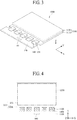
- FIG. 3 is a perspective view illustrating a display device according to one embodiment of the present invention.
- FIG. 4 is a plane view illustrating a first substrate, a gate driver, a source drive IC, a flexible film, a circuit board, and a timing controller of FIG. 3 .
- an organic light emitting display device 1000 includes a display panel 1100, a gate driver 1200, a source drive integrated circuit (hereinafter, referred to as "IC") 1300, a flexible film 1400, a circuit board 1500, and a timing controller 1600.
- the display device according to one embodiment of the present invention may be realized as any one of a liquid crystal display device, an organic light emitting display device, a field emission display device and an electrophoresis display device.
- the display panel 1100 includes a first substrate 1110 and a second substrate 1120.
- the second substrate 1120 may be an encapsulation substrate.
- Each of the first substrate 1110 and the second substrate 1120 may be a plastic film or a glass.
- Gate lines, data lines and pixels P are formed on one surface of the first substrate 1110, which faces the second substrate 1120.
- the pixels P are provided in an area defined by a crossing structure of the gate lines and the data lines.
- the display panel 1100 may be categorized into a display area DA where the pixels are formed to display an image and a non-display area NDA where an image is not displayed, as shown in FIG. 4 .
- the gate lines, the data lines and the pixels may be formed on the display area DA.
- the gate driver 1200, pads, and link lines for connecting the data lines with the pads may be formed on the non-display area NDA.
- the gate driver 1200 supplies gate signals to the gate lines in accordance with a gate control signal input from the timing controller 1600.
- the gate driver 1200 may be formed on the non-display area NDA outside one side or both sides of the display area DA of the display panel 1100 in a gate driver in panel (GIP) mode.
- GIP gate driver in panel
- the source drive IC 1300 receives digital video data and a source control signal from the timing controller 1600.
- the source drive IC 1300 converts the digital video data to analog data voltages in accordance with the source control signal and supplies the analog data voltages to the data lines. If the source drive IC 1300 is fabricated of a driving chip, the source drive IC 1300 may be packaged in the flexible film 1400 in a chip on film (COF) or chip on plastic (COP) mode.
- COF chip on film
- COP chip on plastic
- Pads such as data pads may be formed on the non-display area NDA of the display panel 1100. Lines which connect the pads with the source drive IC 1300 and lines which connect the pads with lines of the circuit board 1500 may be formed in the flexible film 1400.
- the flexible film 1400 may be attached onto the pads by an anisotropic conducting film, whereby the pads may be connected with the lines of the flexible film 1400.
- the circuit board 1500 may be attached to the flexible films 1400.
- a plurality of circuits comprised of driving chips may be packaged in the circuit board 1500.
- the timing controller 1600 may be packaged in the circuit board 1500.
- the circuit board 1500 may be a printed circuit board or a flexible printed circuit board.
- the timing controller 1600 receives digital video data and a timing signal from an external system board through a cable of the circuit board 1500.
- the timing controller 1600 generates a gate control signal for controlling an operation timing of the gate driver 1200 and a source control signal for controlling the source drive ICs 1300 on the basis of the timing signal.
- the timing controller 1600 supplies the gate control signal to the gate driver 1200, and supplies the source control signal to the source drive ICs 1300.
- the pixels P of the display device or the gate driver 1200 may use, for driving, both a thin film transistor having P type semiconductor characteristic and a thin film transistor having N type semiconductor characteristic.
- the pixel P of the organic light emitting display device may include a switching transistor and a driving transistor.
- the switching transistor may be formed of a thin film transistor having N type semiconductor characteristic while the driving transistor may be formed of a thin film transistor having P type semiconductor characteristic.
- the switching transistor may be formed of a thin film transistor having P type semiconductor characteristic while the driving transistor may be formed of a thin film transistor having N type semiconductor characteristic.
- the gate driver may include a CMOS (complementary metal oxide semiconductor) circuit to output gate signals.
- the display device may include a CMOS circuit to output other signals.
- the CMOS circuit includes a first transistor T1 having P type semiconductor characteristic and a second transistor T2 having N type semiconductor characteristic.
- a gate electrode of the first transistor T1 and a gate electrode of the second transistor T2 are connected to an input terminal IT.
- a source electrode of the first transistor T1 is connected to a driving voltage line VDD to which a driving voltage is supplied, and a drain electrode of the first transistor T1 is connected to an output terminal OT.
- a source electrode of the second transistor T2 is connected to a ground GND, and a drain electrode of the second transistor T2 is connected to the output terminal OT.
- the first transistor T1 may be turned on, and the second transistor T2 may be turned off. For this reason, the driving voltage of the driving voltage line VDD may be output to the output terminal OT through the first transistor T1.
- the second transistor T2 may be turned on, and the first transistor T1 may be turned off. For this reason, since the output terminal OT may be connected to the ground GND through the second transistor T, the output terminal OT may be discharged to a ground voltage.
- the first transistor T1 has P type semiconductor characteristic
- the second transistor T2 has N type semiconductor characteristic
- the gate electrode of the first transistor T1 and the gate electrode of the second transistor T2 are connected to the gate electrode, the first transistor T1 and the second transistor T2 may be turned on and turned off complementarily with each other.
- a first thin film transistor that includes an active layer having Sn(II)O based oxide and a second thin film transistor that includes an active layer having Sn(IV)O 2 based oxide are provided.
- the first and second thin film transistors according to the embodiments of the present invention will be described in detail with FIGS. 6 to 24 .
- FIG. 6 is a cross-sectional view illustrating first and second thin film transistors according to the first embodiment of the present invention.
- first and second thin film transistors 10 and 20 are formed in an inverted staggered structure based on a back channel etched (BCE) process.
- the inverted staggered structure has a bottom gate structure in which a gate electrode is formed below an active layer.
- the first thin film transistor 10 includes a first gate electrode 110, a first active layer 130, a metal oxide layer 140, a first source electrode 150, and a first drain electrode 160.
- the second thin film transistor 20 according to the first embodiment of the present invention includes a second gate electrode 210, a second active layer 230, a second source electrode 250, and a second drain electrode 260.
- the first and second thin film transistors 10 and 20 may be formed on a buffer film 100 formed on a substrate.
- the substrate may be formed of plastic or glass.
- the buffer film 100 is intended to protect the first and second thin film transistors 10 and 20 from water permeated through the substrate.
- the buffer film 100 may be made of a plurality of inorganic films which are deposited alternately.
- the buffer film 100 may be formed of a multi-layered film of one or more inorganic films of a silicon oxide film (SiOx), a silicon nitride film (SiNx) and SiON, which are deposited alternately.
- the buffer film 100 may be omitted, and in this case, the first and second thin film transistors 10 and 20 may be formed on the substrate.
- the first and second gate electrodes 110 and 210 are formed on the buffer film 100.
- the first and second gate electrodes 110 and 210 may be formed of a single layer or multi-layer comprised of any one of Mo, Al, Cr, Au, Ti, Ni, Nd and Cu or their alloy.
- a gate insulating film 120 is formed on the first and second gate electrodes 110 and 210.
- the gate insulating film 120 may be formed of an inorganic film, for example, a silicon oxide film (SiOx), a silicon nitride film (SiNx) or a multi-layered film of the silicon oxide film and the silicon nitride film.
- the first and second active layers 130 and 230 are formed on the gate insulating film 120.
- the first active layer 130 may be arranged to overlap the first gate electrode 110, and the second active layer 230 may be arranged to overlap the second gate electrode 210. For this reason, light entering the first active layer 130 from the substrate may be blocked by the first gate electrode 110, and light entering the second active layer 230 may be blocked by the second gate electrode 210.
- the first active layer 130 may be an Sn(II)O based oxide semiconductor layer. That is, the first active layer 130 may be a semiconductor layer that includes an Sn(II)O based oxide.
- the first active layer 130 may include SnO, Sn-M-Ox, Sn-M1-M2-Ox, and SnO doped with M.
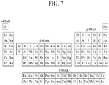
- M, M1, or M2 may be an element of d-Block or an element of p-Block in the periodic table of FIG. 7 .
- M, M1 or M2 may be, but not limited to, any one of W, B, Nb, Al, Ga, Pb and Si.
- the second active layer 230 may be an Sn(IV)O 2 based oxide semiconductor layer. That is, the second active layer 230 may be a semiconductor layer that includes an Sn(IV)O 2 based oxide.
- the second active layer 230 may include SnO 2 , Sn-M-Ox, Sn-M1-M2-Ox, and SnO 2 doped with M.
- M, M1, or M2 may be an element of d-Block or an element of p-Block in the periodic table of FIG. 7 .
- M, M1 or M2 may be, but not limited to, any one of W, B, Nb, Al, Ga, Pb and Si.
- the first active layer 130 is formed of Sn(II)O based oxide semiconductor layer, the first active layer 130 has P type semiconductor characteristic.
- the second active layer 230 is formed of an Sn(IV)O 2 based oxide semiconductor layer, the second active layer 230 has N type semiconductor characteristic.
- the metal oxide layer 140 is formed on the first active layer 130.
- the metal oxide layer 140 is an insulating film which is electrically insulated, and may include metal which is likely to generate oxidation.
- the metal oxide layer 140 may be an aluminum oxide, a titanium oxide, a thallium oxide, or a molybdenum-titanium oxide.
- the first source electrode 150 and the first drain electrode 160 are formed on the metal oxide layer 140. For this reason, the first source electrode 150 may be in contact with the first active layer 130 at a first side of the first active layer 130. The first drain electrode 160 may be in contact with the first active layer 130 at a second side of the first active layer 130.
- the second source electrode 250 and the second drain electrode 260 are formed on the second active layer 230.
- the second source electrode 250 may be in contact with the second active layer 230 at a first side of the second active layer 230.
- the second drain electrode 260 may be in contact with the second active layer 230 at a second side of the second active layer 230.
- the first drain electrode 160 and the second drain electrode 260 may be connected with each other as shown in FIG. 19 .
- the first and second thin film transistors 10 and 20 may serve as CMOS circuits as shown in FIG. 5 .
- An inter-layer dielectric film 170 is formed on the first and second source electrodes 150 and 250 and the first and second drain electrodes 160 and 260.
- the inter-layer dielectric film 170 may be formed of an inorganic film, for example, a silicon oxide film (SiOx), a silicon nitride film (SiNx), or a multi-layered film of the silicon oxide film and the silicon nitride film.
- the first thin film transistor 10 that includes a first active layer 130 having Sn(II)O based oxide and the second thin film transistor 20 that includes a second active layer 230 having Sn(IV)O 2 based oxide are provided.
- the first thin film transistor 10 may be realized as a thin film transistor having P type semiconductor characteristic
- the second thin film transistor 20 may be realized as a thin film transistor having N type semiconductor characteristic.
- FIG. 8 is a flow chart illustrating a method for manufacturing first and second thin film transistors according to the first embodiment of the present invention.
- FIGS. 9a to 9e are cross-sectional views illustrating a method for manufacturing first and second thin film transistors according to the first embodiment of the present invention.
- FIGS. 9a to 9e are intended to describe a method for manufacturing the first and second thin film transistors 10 and 20 shown in FIG. 6 , the same reference numerals are given to the same elements.
- the method for manufacturing the first and second thin film transistors according to the first embodiment of the present invention will be described in detail with reference to FIGS. 8 and 9a to 9e .
- first and second gate electrodes 110 and 210 and a gate insulating film 120 are formed on a buffer film 100.
- the buffer film 100 is intended to protect the first and second thin film transistors 10 and 20 from water permeated through the substrate.
- the buffer film 100 may be made of a plurality of inorganic films which are deposited alternately.
- the buffer film 100 may be formed of a multi-layered film of one or more inorganic films of a silicon oxide film (SiOx), a silicon nitride film (SiNx) and SiON, which are deposited alternately.
- the buffer film 100 may be formed using a plasma enhanced chemical vapor deposition (PECVD) method.
- PECVD plasma enhanced chemical vapor deposition
- the first and second gate electrodes 110 and 210 are formed on the buffer film 100.
- a first metal layer may be formed on an entire surface of the buffer film 100 by sputtering.
- the first metal layer is patterned using a mask process for etching the first metal layer, whereby the first and second gate electrodes 110 and 210 may be formed.
- the first and second gate electrodes 110 and 210 may be formed of a single layer or multi-layer comprised of any one of Mo, Al, Cr, Au, Ti, Ni, Nd and Cu or their alloy.
- a gate insulating film 120 is formed on the first and second gate electrodes 110 and 210.
- the gate insulating film 120 may be formed to cover the first and second gate electrodes 110 and 210.
- the gate insulating film 120 may be formed of an inorganic film, for example, a silicon oxide film (SiOx), a silicon nitride film (SiNx) or a multi-layered film of the silicon oxide film and the silicon nitride film.
- first and second active layers 130 and 230 are formed on the gate insulating film 120.
- a semiconductor layer is formed on the entire surface of the gate insulating film 120 by sputtering or metal organic chemical vapor deposition (MOCVD) method. Then, the semiconductor layer is patterned using a mask process based on a photo resist pattern, whereby the first and second active layers 130 and 230 are formed.
- the first active layer 130 may be arranged to overlap the first gate electrode 110
- the second active layer 230 may be arranged to overlap the second gate electrode 210.
- the first and second active layers 130 and 230 may be formed of SnO 2 , Sn-M-Ox, Sn-M1-M2-Ox, and SnO 2 doped with M.
- M, M1, or M2 may be an element of d-Block or an element of p-Block in the periodic table of FIG. 7 .
- M, M1 or M2 may be, but not limited to, any one of W, B, Nb, Al, Ga, Pb and Si.
- each of the first and second active layers 130 and 230 is formed of an Sn(IV)O 2 based oxide semiconductor layer in step S102 of FIG. 8 , each of them has N type semiconductor characteristic (S102 of FIG. 8 ).
- a reactive metal layer 140' is formed on the first active layer 130.
- a second metal layer may be formed on the gate insulating film 120 and the first and second active layers 130 and 230 by sputtering. Then, after a photo resist pattern is formed on the second metal layer, the second metal layer is patterned using a mask process for etching the second metal layer, whereby the reactive metal layer 140' may be formed.
- the reactive metal layer 140' may be formed of Al, Ti, Ta, or an alloy of Mo and Ti, which is likely to generate oxidation (S103 of FIG. 8 ).
- the first active layer 130 and the reactive metal layer 140' are heat-treated, whereby the first active layer 130 is formed as an Sn(II)O based oxide semiconductor layer, and the reactive metal layer 140' is converted to a metal oxide layer 140.
- the first active layer 130 and the reactive metal layer 140' are heat-treated at a temperature between 200°C and 500°C.
- metal of the reactive metal layer 140' may react with oxygen of the first active layer 130.
- a reduction reaction may be generated in the first active layer 130
- an oxidation reaction may be generated in the reactive metal layer 140'.
- the first active layer 130 may include an Sn(II)O based oxide by means of the reduction reaction
- the reactive metal layer 140' may be converted to the metal oxide layer 140 by means of the oxidation reaction.
- the metal oxide layer 140 may be an aluminum oxide, a titanium oxide, a thallium oxide, or a molybdenum-titanium oxide. That is, the metal oxide layer 140 may be an insulating film which is electrically insulated.
- FIG. 10a Results of XPS (x-ray photoelectron spectroscopy) analysis for the active layer when the reactive metal layer is not formed are shown in FIG. 10a , and graphs and tables illustrating results of XPS analysis for the metal oxide layer and the active layer after the reactive metal layer is formed of titanium and heat-treated at 200°C or 300°C are shown in FIGS. 10b and 10c .
- XPS x-ray photoelectron spectroscopy
- a curve A illustrates that the active layer is ion-etched for 30 seconds and then subjected to XPS analysis
- a curve B illustrates that the metal oxide layer and the active layer are ion-etched for 7 minutes and then subjected to XPS analysis
- a curve C illustrates that the metal oxide layer and the active layer are ion-etched for 17 minutes and then subjected to XPS analysis
- a curve D illustrates that the metal oxide layer and the active layer are ion-etched for 20 minutes and then subjected to XPS analysis.
- Ion-etching may be performed using Ar ion.
- a curve A illustrates that the active layer is ion-etched for 60 minutes at 200°C and then subjected to XPS analysis
- a curve B illustrates that the metal oxide layer and the active layer are ion-etched for 66 minutes and then subjected to XPS analysis
- a curve C illustrates that the metal oxide layer and the active layer are ion-etched for 77 minutes and then subjected to XPS analysis
- a curve D illustrates that the metal oxide layer and the active layer are ion-etched for 81 minutes and then subjected to XPS analysis.
- a curve A illustrates that the active layer is ion-etched for 69 minutes at 300°C and then subjected to XPS analysis
- a curve B illustrates that the metal oxide layer and the active layer are ion-etched for 74 minutes and then subjected to XPS analysis
- a curve C illustrates that the metal oxide layer and the active layer are ion-etched for 85 minutes and then subjected to XPS analysis
- a curve D illustrates that the metal oxide layer and the active layer are ion-etched for 91 minutes and then subjected to XPS analysis.
- a binding energy (BE) of Sn2+ has a value between 484nm and 485nm and between 493nm and 493nm, approximately.
- XPS analysis is an analysis method for obtaining a binding energy of metal to be analyzed by irradiating X-ray to the metal. If an ion-etching time is short, a binding energy on a metal surface or interface may be obtained, and if the ion-etching time is long, a binding energy inside the metal may be obtained. Therefore, if the reactive metal layer 140' is formed of titanium on the first active layer 130, X-ray may be irradiated for 60 minutes or more as shown in FIGS. 10b and 10c for XPS analysis of the first active layer 130.
- the reactive metal layer 140' is not formed, as a result of XPS analysis of the first active layer 130, a peak at a binding energy of Sn 2+ is not generated as shown in FIG. 10a . Therefore, if the reactive metal layer 140' is not formed, it may be regarded that Sn(II)O does not exist in the first active layer.
- the reactive metal layer 140' is formed of titanium and is heat-treated at 200°C together with the first active layer 130, a peak at a binding energy of Sn 2+ of the curve A and the curve B is generated as shown in FIGS. 10b and 10d . Therefore, if the reactive metal layer 140' and the first active layer 130 are heat-treated at 200°C, it may be regarded that Sn(II)O exists on the interface of the first active layer 130. That is, since the first active layer 130 may include an Sn(II)O based oxide, the first active layer 130 may have P type semiconductor characteristic.
- the reactive metal layer 140' is formed of titanium and is heat-treated at 300°C together with the first active layer 130, a peak at a binding energy of Sn 2+ of all the curves A to D is generated as shown in FIGS. 10c and 10d . Therefore, if the reactive metal layer 140' and the first active layer 130 are heat-treated at 300°C, it may be regarded that Sn(II)O exists on the interface of the first active layer 130 and inside the first active layer 130. That is, since the first active layer 130 may include an Sn(II)O based oxide, the first active layer 130 may have P type semiconductor characteristic.
- FIGS. 11a to 11d Graphs and tables illustrating results of XPS analysis for the active layer when the reactive metal layer is not formed and when the reactive metal layer is formed of titanium and heat-treated at 200°C or 300°C are shown in FIGS. 11a to 11d .
- a curve A illustrates that the active layer is ion-etched for 30 seconds and then subjected to XPS analysis
- a curve B illustrates that the metal oxide layer and the active layer are ion-etched for 7 minutes and then subjected to XPS analysis
- a curve C illustrates that the metal oxide layer and the active layer are ion-etched for 17 minutes and then subjected to XPS analysis
- a curve D illustrates that the metal oxide layer and the active layer are ion-etched for 20 minutes and then subjected to XPS analysis.
- a curve A illustrates that the active layer is ion-etched for 31 minutes at 200°C and then subjected to XPS analysis
- a curve B illustrates that the metal oxide layer and the active layer are ion-etched for 32 minutes and then subjected to XPS analysis
- a curve C illustrates that the metal oxide layer and the active layer are ion-etched for 37 minutes and then subjected to XPS analysis
- a curve D illustrates that the metal oxide layer and the active layer are ion-etched for 40 minutes and then subjected to XPS analysis.
- a curve A illustrates that the active layer is ion-etched for 35 minutes at 300°C and then subjected to XPS analysis
- a curve B illustrates that the metal oxide layer and the active layer are ion-etched for 36 minutes and then subjected to XPS analysis
- a curve C illustrates that the metal oxide layer and the active layer are ion-etched for 38 minutes and then subjected to XPS analysis
- a curve D illustrates that the metal oxide layer and the active layer are ion-etched for 40 minutes and then subjected to XPS analysis.
- a binding energy (BE) of Sn 2+ has a value between 484nm and 485nm and between 493nm and 493nm, approximately.
- XPS analysis is an analysis method for obtaining a binding energy of metal to be analyzed by irradiating X-ray to the metal. If an ion-etching time is short, a binding energy on a metal surface or interface may be obtained, and if the ion-etching time is long, a binding energy inside the metal may be obtained. Therefore, if the reactive metal layer 140' is formed of titanium on the first active layer 130, X-ray may be irradiated for 30 minutes or more as shown in FIGS. 11b and 11c for XPS analysis of the first active layer 130.
- the reactive metal layer 140' is not formed, as a result of XPS analysis of the first active layer 130, a peak at a binding energy of Sn 2+ is not generated as shown in FIG. 11a . Therefore, if the reactive metal layer 140' is not formed, it may be regarded that Sn(II)O does not exist in the first active layer.
- the reactive metal layer 140' is formed of titanium and is heat-treated at 200°C together with the first active layer 130, a peak at a binding energy of Sn 2+ of the curve A and the curve B is generated as shown in FIGS. 11b and 11d . Therefore, if the reactive metal layer 140' and the first active layer 130 are heat-treated at 200°C, it may be regarded that Sn(II)O exists on the interface of the first active layer 130. That is, since the first active layer 130 may include an Sn(II)O based oxide, the first active layer 130 may have P type semiconductor characteristic.
- the reactive metal layer 140' is formed of titanium and is heat-treated at 300°C together with the first active layer 130, a peak at a binding energy of Sn 2+ of all the curves A to D is generated as shown in FIGS. 11c and 11d . Therefore, if the reactive metal layer 140' and the first active layer 130 are heat-treated at 300°C, it may be regarded that Sn(II)O exists on the interface of the first active layer 130 and inside the first active layer 130. That is, since the first active layer 130 may include an Sn(II)O based oxide, the first active layer 130 may have P type semiconductor characteristic.
- the reactive metal layer 140' is formed on the first active layer 130 and then heat-treated at a temperature between 200°C and 500°C, whereby oxidation reaction may be generated in the reactive metal layer 140' and reduction reaction may be generated in the first active layer 130.
- the first active layer 130 may be formed of an Sn(II)O based oxide semiconductor layer. Therefore, in the embodiment of the present invention, an Sn(II)O based oxide semiconductor transistor having P type semiconductor characteristic may be formed (S104 of FIG. 8 ).
- first and second source electrodes 150 and 250 and first and second drain electrodes 160 and 260 are formed on the first and second active layers 130 and 230.
- a third metal layer is formed on the gate insulating film 120, the first and second active layers 130 and 230 and the metal oxide layer 140 by sputtering or metal organic chemical vapor deposition (MOCVD) method. Then, the third metal layer is patterned using a mask process based on a photo resist pattern, whereby the first and second source electrodes 150 and 250 and the first and second drain electrodes 160 and 260 are formed.
- MOCVD metal organic chemical vapor deposition
- the first source electrode 150 may be in contact with the first active layer 130 at a first side of the first active layer 130.
- the first drain electrode 160 may be in contact with the first active layer 130 at a second side of the first active layer 130.
- the first source electrode 150 may be in contact with, but not limited to, an upper surface of the metal oxide layer 140 and the first side of the first active layer 130
- the first drain electrode 160 may be in contact with, but not limited to, the upper surface of the metal oxide layer 140 and the second side of the first active layer 130.
- the second source electrode 250 may be in contact with the second active layer 230 at a first side of the second active layer 230.
- the second drain electrode 260 may be in contact with the second active layer 230 at a second side of the second active layer 230.
- the second source electrode 250 may be in contact with, but not limited to, an upper surface and the first side of the second active layer 230
- the second drain electrode 260 may be in contact with, but not limited to, the upper surface and the second side of the second active layer 230.
- the first drain electrode 160 and the second drain electrode 260 may be connected with each other.
- the first and second thin film transistors 10 and 20 may serve as CMOS circuits as shown in FIG. 5 .
- the first and second source electrodes 150 and 250 and the first and second drain electrodes 160 and 260 may be formed of a single layer or multi-layer comprised of any one of Mo, Al, Cr, Au, Ti, Ni, Nd and Cu or their alloy. However, since the first source electrode 150 and the first drain electrode 160 are in contact with the first active layer 130 having P type semiconductor characteristic, the first and second source electrodes 150 and 250 and the first and second drain electrodes 160 and 260 may be formed of a single layer or multi-layer comprised of any one of Pd (5.22eV or 5.6eV), Pt (5.12eV to 5.93eV), Au (5.1eV to 5.47eV), and Ni (5.04eV to 5.35eV), which are greater than a work function of 5.0eV, or their alloy.
- an inter-layer dielectric film 170 is formed on the first and second source electrodes 150 and 250 and the first and second drain electrodes 160 and 260.
- the inter-layer dielectric film 170 may be formed of an inorganic film, for example, a silicon oxide film (SiOx), a silicon nitride film (SiNx), or a multi-layered film of the silicon oxide film and the silicon nitride film (S105 of FIG. 8 ).
- the reactive metal layer 140' is formed on the first active layer 130 and then heat-treated at a temperature between 200°C and 500°C, whereby the oxidation reaction may be generated in the reactive metal layer 140' and the reduction reaction may be generated in the first active layer 130.
- the first active layer 130 may be formed of an Sn(II)O based oxide semiconductor layer. Therefore, in the embodiment of the present invention, an Sn(II)O based oxide semiconductor transistor having P type semiconductor characteristic may be formed.
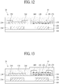
- FIG. 12 is a cross-sectional view illustrating first and second thin film transistors according to the second embodiment of the present invention.
- first and second thin film transistors 10 and 20 are formed in an inverted staggered structure based on a back channel etched (BCE) process.
- the inverted staggered structure has a bottom gate structure in which a gate electrode is formed below an active layer.
- the first thin film transistor 10 includes a first gate electrode 110, a first active layer 130, a metal oxide layer 140, a first source electrode 150, and a first drain electrode 160.
- the second thin film transistor 20 according to the second embodiment of the present invention includes a second gate electrode 210, a second active layer 230, a second source electrode 250, and a second drain electrode 260.
- the second embodiment of FIG. 12 is substantially the same as the first embodiment described with reference to FIG. 6 except that the metal oxide layer 140 is formed below the first active layer 130. Therefore, a detailed description of FIG. 12 will be omitted.
- a method for manufacturing the first and second thin film transistors 10 and 20 according to the second embodiment of the present invention is substantially the same as the method described with reference to FIGS. 8 and 9a to 9e except that the order of the steps S102 and S103 of FIG. 8 is changed. Therefore, a detailed description of the method for manufacturing the first and second thin film transistors 10 and 20 according to the second embodiment of the present invention will be omitted.
- FIG. 13 is a cross-sectional view illustrating first and second thin film transistors according to the third embodiment of the present invention.
- first and second thin film transistors 10 and 20 are formed in an inverted staggered structure based on a back channel etched (BCE) process.
- the inverted staggered structure has a bottom gate structure in which a gate electrode is formed below an active layer.
- the first thin film transistor 10 includes a first gate electrode 110, a first active layer 130, a metal oxide layer 140, a first source electrode 150, and a first drain electrode 160.
- the second thin film transistor 20 according to the third embodiment of the present invention includes a second gate electrode 210, a second active layer 230, a second source electrode 250, and a second drain electrode 260.
- the third embodiment of FIG. 13 is substantially the same as the first embodiment described with reference to FIG. 6 except that a first metal oxide layer 141 is formed below the first active layer 130 and a second metal oxide layer 142 is formed on the first active layer 130. As shown in FIG. 13 , if the first and second metal oxide layers 141 and 142 are formed below and on the first active layer 130, a reduction reaction is generated below and on the first active layer 130, whereby a time period for forming the first active layer 130 as Sn(II)O based oxide semiconductor layer may be reduced.
- a method for manufacturing the first and second thin film transistors 10 and 20 according to the third embodiment of the present invention is substantially the same as the method described with reference to FIGS. 8 and 9a to 9e except that the first metal oxide layer 141 is additionally formed prior to the step S102 of FIG. 8 . Therefore, a detailed description of the method for manufacturing the first and second thin film transistors 10 and 20 according to the third embodiment of the present invention will be omitted.
- FIG. 14 is a cross-sectional view illustrating first and second thin film transistors according to the fourth embodiment of the present invention.
- first and second thin film transistors 10 and 20 are formed in a coplanar structure.
- the coplanar structure has a top gate structure in which a gate electrode is formed on an active layer.
- the first thin film transistor 10 includes a first gate electrode 110, a first active layer 130, a metal oxide layer 140, a first source electrode 150, and a first drain electrode 160.
- the second thin film transistor 20 according to the fourth embodiment of the present invention includes a second gate electrode 210, a second active layer 230, a second source electrode 250, and a second drain electrode 260.
- the first and second thin film transistors 10 and 20 may be formed on a buffer film 100 formed on a substrate.
- the substrate may be formed of plastic or glass.
- the buffer film 100 is intended to protect the first and second thin film transistors 10 and 20 from water permeated through the substrate.
- the buffer film 100 may be made of a plurality of inorganic films which are deposited alternately.
- the buffer film 100 may be formed of a multi-layered film of one or more inorganic films of a silicon oxide film (SiOx), a silicon nitride film (SiNx) and SiON, which are deposited alternately.
- the buffer film 100 may be omitted, and in this case, the first and second thin film transistors 10 and 20 may be formed on the substrate.
- the first and second active layers 130 and 230 are formed on the buffer film 100.
- the first active layer 130 may be an Sn(II)O based oxide semiconductor layer. That is, the first active layer 130 may be a semiconductor layer that includes Sn(II)O based oxide.
- the first active layer 130 may include SnO, Sn-M-Ox, Sn-M1-M2-Ox, and SnO doped with M.
- M, M1, or M2 may be an element of d-Block or an element of p-Block in the periodic table of FIG. 7 .
- M, M1 or M2 may be, but not limited to, any one of W, B, Nb, Al, Ga, Pb and Si.
- the second active layer 230 may be an Sn(IV)O 2 based oxide semiconductor layer. That is, the second active layer 230 may be a semiconductor layer that includes an Sn(IV)O 2 based oxide.
- the second active layer 230 may include SnO 2 , Sn-M-Ox, Sn-M1-M2-Ox, and SnO 2 doped with M.
- M, M1, or M2 may be an element of d-Block or an element of p-Block in the periodic table of FIG. 7 .
- M, M1 or M2 may be, but not limited to, any one of W, B, Nb, Al, Ga, Pb and Si.
- the first active layer 130 is formed of an Sn(II)O based oxide semiconductor layer
- the first active layer 130 has P type semiconductor characteristic
- the second active layer 230 is formed of an Sn(IV)O 2 based oxide semiconductor layer
- the second active layer 230 has N type semiconductor characteristic.
- the metal oxide layer 140 is formed on the first active layer 130.
- the metal oxide layer 140 is formed on a part of an upper surface of the first active layer 130, and the upper surface of the first active layer 130, which is not covered with the metal oxide layer 140, may be defined as a conductive area having conductivity.
- the metal oxide layer 140 is an insulating film which is electrically insulated, and may include metal which is likely to generate oxidation.
- the metal oxide layer 140 may be an aluminum oxide, a titanium oxide, a thallium oxide, or a molybdenum-titanium oxide.
- a gate insulating film 120 is formed on the metal oxide layer 140.
- the gate insulating film 120 may be formed of an inorganic film, for example, a silicon oxide film (SiOx), a silicon nitride film (SiNx) or a multi-layered film of the silicon oxide film and the silicon nitride film.
- the first and second gate electrodes 110 and 210 are formed on the gate insulating film 120.
- the first gate electrode 110 may be arranged to overlap the first active layer 130, and the second gate electrode 210 may be arranged to overlap the second active layer 230.
- the first and second gate electrodes 110 and 210 may be formed of a single layer or multi-layer comprised of any one of Mo, Al, Cr, Au, Ti, Ni, Nd and Cu or their alloy.
- An inter-layer dielectric film 170 is formed on the first and second active layers 130 and 230 and the first and second gate electrodes 110 and 210.
- the inter-layer dielectric film 170 may be formed of an inorganic film, for example, a silicon oxide film (SiOx), a silicon nitride film (SiNx), or a multi-layered film of the silicon oxide film and the silicon nitride film.
- the first and second source electrodes 150 and 250 and the first and second drain electrodes 160 and 260 are formed on the inter-layer dielectric film 170.
- First and second contact holes CT1 and CT2 for partially exposing the first active layer 130 by passing through the inter-layer dielectric film 170 and third and fourth contact holes CT3 and CT4 for partially exposing the second active layer 230 are formed in the inter-layer dielectric film 170.
- the first source electrode 150 may be in contact with the first active layer 130 at a first side of the first active layer 130 through the first contact hole CT1.
- the first drain electrode 160 may be in contact with the first active layer 130 at a second side of the first active layer 130 through the second contact hole CT2. Also, each of the first source electrode 150 and the first drain electrode 160 may be in contact with a conducting area 131 of the first active layer 130.
- the second source electrode 250 may be in contact with the second active layer 230 at a first side of the second active layer 230 through the third contact hole CT3.
- the second drain electrode 260 may be in contact with the second active layer 230 at a second side of the second active layer 230 through the fourth contact hole CT4.
- each of the second source electrode 250 and the second drain electrode 260 may be in contact with a conducting area 231 of the second active layer 230.
- the first drain electrode 160 and the second drain electrode 260 may be connected with each other on the inter-layer dielectric film 170, or the first active layer 130 and the second active layer 230 may be connected with each other as shown in FIG. 20 .
- the first and second thin film transistors 10 and 20 may serve as CMOS circuits as shown in FIG. 5 .
- the first thin film transistor 10 that includes a first active layer 130 having an Sn(II)O based oxide and the second thin film transistor 20 that includes a second active layer 230 having an Sn(IV)O 2 based oxide are provided.
- the first thin film transistor 10 may be realized as a thin film transistor having P type semiconductor characteristic
- the second thin film transistor 20 may be realized as a thin film transistor having N type semiconductor characteristic.
- FIG. 15 is a flow chart illustrating a method for manufacturing first and second thin film transistors according to the fourth embodiment of the present invention.
- FIGS. 16a to 16d are cross-sectional views illustrating a method for manufacturing first and second thin film transistors according to the fourth embodiment of the present invention.
- FIGS. 16a to 16d are intended to describe a method for manufacturing the first and second thin film transistors 10 and 20 shown in FIG. 14 , the same reference numerals are given to the same elements.
- the method for manufacturing the first and second thin film transistors according to the fourth embodiment of the present invention will be described in detail with reference to FIGS. 15 and 16a to 16d .
- first and second active layers 130 and 230 are formed on a buffer film 100.
- the buffer film 100 is intended to protect the first and second thin film transistors 10 and 20 from water permeated through a substrate.
- the buffer film 100 may be made of a plurality of inorganic films which are deposited alternately.
- the buffer film 100 may be formed of a multi-layered film of one or more inorganic films of a silicon oxide film (SiOx), a silicon nitride film (SiNx) and SiON, which are deposited alternately.
- the buffer film 100 may be formed using a plasma enhanced chemical vapor deposition (PECVD) method.
- PECVD plasma enhanced chemical vapor deposition
- the first and second active layers 130 and 230 are formed on the buffer film 100.
- a semiconductor layer is formed on an entire surface of the gate insulating film 120 by sputtering or MOCVD method. Then, the semiconductor layer is patterned using a mask process based on a photo resist pattern, whereby the first and second active layers 130 and 230 are formed.
- the first and second active layers 130 and 230 may be formed of SnO 2 , Sn-M-Ox, Sn-M1-M2-Ox, and SnO 2 doped with M.
- M, M1, or M2 may be an element of d-Block or an element of p-Block in the periodic table of FIG. 7 .
- M, M1 or M2 may be, but not limited to, any one of W, B, Nb, Al, Ga, Pb and Si.
- each of the first and second active layers 130 and 230 is formed of an Sn(IV)O 2 based oxide semiconductor layer in step S201 of FIG. 15 , each of them has N type semiconductor characteristic (S201 of FIG. 15 ).
- a reactive metal layer 140' is formed on the first active layer 130.
- a first metal layer may be formed on the gate insulating film 120 and the first and second active layers 130 and 230 by sputtering. Then, after a photo resist pattern is formed on the first metal layer, the first metal layer is patterned using a mask process for etching the first metal layer, whereby the reactive metal layer 140' may be formed.
- the reactive metal layer 140' may be formed of Al, Ti, Ta, or an alloy of Mo and Ti, which is likely to generate oxidation (S202 of FIG. 15 ).
- the first active layer 130 and the reactive metal layer 140' are heat-treated, whereby the first active layer 130 is formed as an Sn(II)O based oxide semiconductor layer, and the reactive metal layer 140' is converted to a metal oxide layer 140.
- the first active layer 130 and the reactive metal layer 140' are heat-treated at a temperature between 200°C and 500°C.
- metal of the reactive metal layer 140' may react with oxygen of the first active layer 130.
- a reduction reaction may be generated in the first active layer 130
- an oxidation reaction may be generated in the reactive metal layer 140'.
- the first active layer 130 may include an Sn(II)O based oxide by means of the reduction reaction
- the reactive metal layer 140' may be converted to the metal oxide layer 140 by means of the oxidation reaction.
- the metal oxide layer 140 may be an aluminum oxide, a titanium oxide, a thallium oxide, or a molybdenum-titanium oxide. (S103 of FIG. 15 )
- the gate insulating film 120, the first and second gate electrodes 110 and 210, the inter-layer dielectric film 170, the first and second source electrodes 150 and 250, and the first and second drain electrodes 160 and 260 are formed as shown in FIG. 16d .
- the gate insulating film 120 and the first and second gate electrodes 110 and 210 are formed on the second active layer 230 and the metal oxide layer 140.
- the gate insulating film 120 and the second metal layer may be formed on the first and second active layers and the metal oxide layer 140.
- the second metal layer and the gate insulating film 120 are patterned using a mask process for etching the second metal layer and the second gate insulating film 120, whereby the gate insulating film 120 and the first and second gate electrodes 110 and 210 may be formed.
- the metal oxide layer which is not covered with the first gate electrode 110 and the gate insulating film 120 may be etched by an etching process. Also, upper surfaces of the first and second active layers 130 and 230, which are not covered with the first gate electrode 110 and the gate insulating film 120, may have conductivity by an etching process.
- the gate insulating film 120 may be formed of an inorganic film, for example, a silicon oxide film (SiOx), a silicon nitride film (SiNx) or a multi-layered film of the silicon oxide film and the silicon nitride film.
- the first and second gate electrodes 110 and 210 may be formed of a single layer or multi-layer comprised of any one of Mo, Al, Cr, Au, Ti, Ni, Nd and Cu or their alloy.
- the inter-layer dielectric film 170 is formed on the first and second active layers 130 and 230 and the first and second gate electrodes 110 and 210.
- the inter-layer dielectric film 170 may be formed of an inorganic film, for example, a silicon oxide film (SiOx), a silicon nitride film (SiNx), or a multi-layered film of the silicon oxide film and the silicon nitride film.
- the inter-layer dielectric film 170 may be formed using a plasma enhanced chemical vapor deposition (PECVD) method.
- first and second contact holes CT1 and CT2 for partially exposing the first active layer 130 and third and fourth contact holes CT3 and CT4 for partially exposing the second active layer 230 are formed to pass through the inter-layer dielectric film 170.
- First and second source electrodes 150 and 250 and first and second drain electrodes 160 and 260 may be formed on the inter-layer dielectric film 170.
- a third metal layer is formed on the inter-layer dielectric film 170 by sputtering or metal organic chemical vapor deposition (MOCVD) method. Then, the third metal layer is patterned using a mask process based on a photo resist pattern, whereby the first and second source electrodes 150 and 250 and the first and second drain electrodes 160 and 260 are formed.
- MOCVD metal organic chemical vapor deposition
- the first source electrode 150 may be in contact with the first active layer 130 at a first side of the first active layer 130 through the first contact hole CT1.
- the first drain electrode 160 may be in contact with the first active layer 130 at a second side of the first active layer 130 through the second contact hole CT2. Also, each of the first source electrode 150 and the first drain electrode 160 may be in contact with a conducting area 131 of the first active layer 130.
- the second source electrode 250 may be in contact with the second active layer 230 at a first side of the second active layer 230 through the third contact hole CT3.
- the second drain electrode 260 may be in contact with the second active layer 230 at a second side of the second active layer 230 through the fourth contact hole CT4.
- each of the second source electrode 250 and the second drain electrode 260 may be in contact with a conducting area 231 of the second active layer 230.
- the first drain electrode 160 and the second drain electrode 260 may be connected with each other on the inter-layer dielectric film 170.
- the first and second thin film transistors 10 and 20 may serve as CMOS circuits as shown in FIG. 5 .
- the first and second source electrodes 150 and 250 and the first and second drain electrodes 160 and 260 may be formed of a single layer or multi-layer comprised of any one of Mo, Al, Cr, Au, Ti, Ni, Nd and Cu or their alloy. However, since the first source electrode 150 and the first drain electrode 160 are in contact with the first active layer 130 having P type semiconductor characteristic, the first and second source electrodes 150 and 250 and the first and second drain electrodes 160 and 260 may be formed of a single layer or multi-layer comprised of any one of Pd (5.22eV or 5.6eV), Pt (5.12eV to 5.93eV), Au (5.1eV to 5.47eV), and Ni (5.04eV to 5.35eV), which are greater than a work function of 5.0eV, or their alloy. (S204 of FIG. 15 )
- the reactive metal layer 140' is formed on the first active layer 130 and then heat-treated at a temperature between 200°C and 500°C, whereby the oxidation reaction may be generated in the reactive metal layer 140' and the reduction reaction may be generated in the first active layer 130.
- the first active layer 130 may be formed of an Sn(II)O based oxide semiconductor layer. Therefore, in the embodiment of the present invention, an Sn(II)O based oxide semiconductor transistor having P type semiconductor characteristic may be formed.
- FIG. 17 is a cross-sectional view illustrating first and second thin film transistors according to the fifth embodiment of the present invention.
- first and second thin film transistors 10 and 20 are formed in a coplanar structure.
- the coplanar structure has a top gate structure in which a gate electrode is formed on an active layer.
- the first thin film transistor 10 includes a first gate electrode 110, a first active layer 130, a metal oxide layer 140, a first source electrode 150, and a first drain electrode 160.
- the second thin film transistor 20 according to the fifth embodiment of the present invention includes a second gate electrode 210, a second active layer 230, a second source electrode 250, and a second drain electrode 260.
- the fifth embodiment of FIG. 17 is substantially the same as the fourth embodiment described with reference to FIG. 14 except that the metal oxide layer 140 is formed below the first active layer 130. Therefore, a detailed description of FIG. 17 will be omitted.
- a method for manufacturing the first and second thin film transistors 10 and 20 according to the fifth embodiment of the present invention is substantially the same as the method described with reference to FIGS. 15 and 16a to 16d except that the order of the steps S201 and S202 of FIG. 14 is changed. Therefore, a detailed description of the method for manufacturing the first and second thin film transistors 10 and 20 according to the fifth embodiment of the present invention will be omitted.
- FIG. 18 is a cross-sectional view illustrating first and second thin film transistors according to the sixth embodiment of the present invention.
- first and second thin film transistors 10 and 20 are formed in a coplanar structure.
- the coplanar structure has a top gate structure in which a gate electrode is formed on an active layer.
- the first thin film transistor 10 includes a first gate electrode 110, a first active layer 130, a first metal oxide layer 141, a second metal oxide layer 142, a first source electrode 150, and a first drain electrode 160.
- the second thin film transistor 20 according to the sixth embodiment of the present invention includes a second gate electrode 210, a second active layer 230, a second source electrode 250, and a second drain electrode 260.
- the sixth embodiment of FIG. 18 is substantially the same as the fourth embodiment described with reference to FIG. 14 except that the first metal oxide layer 141 is formed below the first active layer 130 and the second metal oxide layer 142 is formed on the first active layer 130. Therefore, a detailed description of FIG. 18 will be omitted.
- a method for manufacturing the first and second thin film transistors 10 and 20 according to the sixth embodiment of the present invention is substantially the same as the method described with reference to FIGS. 15 and 16a to 16d except that the step of forming the first metal layer 141 is added prior to the step of S201 of FIG. 14 . Therefore, a detailed description of the method for manufacturing the first and second thin film transistors 10 and 20 according to the sixth embodiment of the present invention will be omitted.
- the reactive metal layer is formed on the first active layer and then heat-treated at a temperature between 200°C and 500°C, whereby the oxidation reaction may be generated in the reactive metal layer and the reduction reaction may be generated in the first active layer.
- the first active layer may be formed of Sn(II)O based oxide semiconductor layer. Therefore, in the embodiment of the present invention, Sn(II)O based oxide semiconductor transistor having P type semiconductor characteristic may be formed.
- the first thin film transistor that includes a first active layer having an Sn(II)O based oxide and the second thin film transistor that includes a second active layer having an Sn(IV)O 2 based oxide are provided.
- the first thin film transistor may be realized as a thin film transistor having P type semiconductor characteristic
- the second thin film transistor may be realized as a thin film transistor having N type semiconductor characteristic.
Landscapes
- Thin Film Transistor (AREA)
- Chemical & Material Sciences (AREA)
- Crystallography & Structural Chemistry (AREA)
Abstract
Description
- This application claims the benefit of the Korean Patent Application No.
10-2016-0183661 filed on December 30, 2016 - The present invention relates to a thin film transistor and a method for manufacturing the same, and a display device including the same.
- Recently, with the advancement of the information age, a demand for a display device for displaying an image has been increased in various forms. Therefore, various flat panel display devices such as liquid crystal display (LCD) devices, plasma display panel (PDP) devices, and organic light emitting display (OLED) devices have been used.
- The flat panel display device such as the liquid crystal display device and the organic light emitting display device includes a display panel, a gate driving circuit, a data driving circuit, and a timing controller. The display panel includes data lines, gate lines, and a plurality of pixels formed at crossing portions of the data lines and the gate lines, receiving data voltages of the data lines when gate signals are supplied to the gate lines. The pixels emit light at a predetermined brightness in accordance with the data voltages.
- Also, the flat panel display device is a switching device, and drives the pixels and the gate driving circuit using a thin film transistor. The thin film transistor may be a metal oxide semiconductor field effect transistor (MOSFET, hereinafter, referred to as "oxide semiconductor transistor") that controls a flow of a current by means of an electric field.
- In the gate driving circuit or data driving circuit of the flat panel display device, a complementary metal oxide semiconductor (CMOS) which is an inverter may be used to properly output a signal which is input. The CMOS requires both an N type oxide semiconductor transistor and a P type oxide semiconductor transistor.
- However, an indium gallium zinc oxide (IGZO) based oxide semiconductor transistor has N type semiconductor characteristic as shown in
FIG. 1 but does not have P type semiconductor characteristic. Therefore, it is difficult to form a thin film transistor having P type semiconductor characteristic by using the IGZO based oxide semiconductor transistor. - Also, an Sn based oxide may exist as Sn(IV)O2 and Sn(II)O. Sn(IV)O2 has N type semiconductor characteristic, and Sn(II)O has P type semiconductor characteristic. However, as shown in
FIG. 2 , since gibbs free energy of Sn(IV)O2 is lower than that of Sn(II)O, Sn(II)O is easily transited to Sn(IV)O2 having low gibbs free energy. Therefore, it is not easy to form a thin film transistor having P type semiconductor characteristic by using Sn based oxide semiconductor transistor. - Accordingly, the present invention is directed to a thin film transistor and a method for manufacturing the same, and a display device including the same, which substantially obviate one or more problems due to limitations and disadvantages of the related art.
- An advantage of the present invention is to provide a thin film transistor and a method for manufacturing the same, and a display device including the same, in which P type semiconductor characteristic is realized using an active layer that includes an Sn based oxide.
- Additional advantages and features of the invention will be set forth in part in the description which follows and in part will become apparent to those having ordinary skill in the art upon examination of the following or may be learned from practice of the invention. The objectives and other advantages of the invention may be realized and attained by the structure particularly pointed out in the written description and claims hereof as well as the appended drawings.
- The object is solved by the features of the independent claims. Preferred embodiments are given in the dependent claims.
- To achieve these objects and other advantages and in accordance with the purpose of the invention, as embodied and broadly described herein, there is provided a thin film transistor comprising an active layer that includes an Sn(II)O based oxide; a metal oxide layer being in contact with one surface of the active layer; a gate electrode overlapped with the active layer; a gate insulating film provided between the gate electrode and the active layer; a source electrode being in contact with a first side of the active layer; and a drain electrode being in contact with a second side of the active layer.
- In another aspect of the present invention, there is provided a method for manufacturing a thin film transistor, which comprises the steps of forming a gate electrode and forming a gate insulating film covering the gate electrode; forming an active layer on the gate insulating film; forming a reactive metal layer on the active layer; forming the active layer as an Sn(II)O based oxide semiconductor layer and forming the reactive metal layer as a metal oxide layer by heat-treating the active layer and the reactive metal layer; and forming a source electrode which is in contact with a first side of the active layer and a drain electrode which is in contact with a second side of the active layer. In other aspect of the present invention, there is provided a display device comprising a first thin film transistor having P type semiconductor characteristic; and a second thin film transistor having N type semiconductor characteristic, wherein the first thin film transistor includes a first active layer having an Sn(II)O based oxide, and the second thin film transistor includes a second active layer having an Sn(IV)O2 based oxide.
- Preferably, the metal oxide layer is an insulating layer which is electrically insulated.
- Preferably, the metal oxide layer is formed of an aluminum oxide, a titanium oxide, a thallium oxide, or a molybdenum-titanium oxide.
- Preferably, the metal oxide layer is provided on an upper surface of the active layer. Thus, the metal oxide layer is arranged on far side surface of the active layer or the averted surface with respect to a surface facing the gate insulation layer or the first gate electrode.
- Preferably, the source electrode and the drain electrode are in contact with the metal oxide layer.
- Preferably, the gate electrode is arranged below the active layer.
- Preferably, the metal oxide layer is provided on a part of the upper surface of the active layer.
- Preferably, the upper surface of the active layer, which is not covered with the metal oxide layer is conducted.
- Preferably, the source electrode and the drain electrode are in contact with a conducting area of the active layer.
- Preferably, the gate electrode is arranged on the active layer.
- Preferably, the metal oxide layer is provided below the active layer.
- Preferably, a method for manufacturing a thin film transistor is provided, the method comprising the steps of: forming an active layer; forming a reactive metal layer on the active layer; forming the active layer as an Sn(II)O based oxide semiconductor layer and forming the reactive metal layer as a metal oxide layer by heat-treating the active layer and the reactive metal layer; and forming a gate insulating layer covering the metal oxide layer and forming a gate electrode layer on the gate insulating layer, and forming a gate electrode and a gate insulating film by etching the gate electrode layer and the gate insulating layer; forming an inter-layer dielectric film on the gate electrode; and forming first and second contact holes for exposing the active layer by passing through the inter-layer insulating film, and forming a source electrode, which is in contact with a first side of the active layer, through the first contact hole and a drain electrode, which is in contact with a second side of the active layer, through the second contact hole.
- Preferably, the first thin film transistor includes: a metal oxide layer which is in contact with one surface of the first active layer; a first gate electrode overlapped with the first active layer; a gate insulating film provided between the first gate electrode and the first active layer; a first source electrode which is in contact with a first side of the first active layer; and a first drain electrode which is in contact with a second side of the first active layer.
- Preferably, the second thin film transistor includes: a second gate electrode overlapped with the second active layer; a gate insulating film provided between the second gate electrode and the second active layer; a second source electrode which is in contact with a first side of the second active layer; and a second drain electrode which is in contact with a second side of the second active layer.
- Preferably, the metal oxide layer is an insulating layer which is electrically insulated.
- Preferably, the metal oxide layer is provided on an upper surface of the second active layer.
- Preferably, the metal oxide layer is provided below the second active layer.
- It is to be understood that both the foregoing general description and the following detailed description of the present invention are exemplary and explanatory and are intended to provide further explanation of the invention as claimed.
- The accompanying drawings, which are included to provide a further understanding of the invention and are incorporated in and constitute a part of this application, illustrate embodiment(s) of the invention and together with the description serve to explain the principle of the invention. In the drawings:
-
FIG. 1 is a graph illustrating semiconductor characteristic of an IGZO based oxide semiconductor transistor; -
FIG. 2 is a table illustrating gibbs free energy of each of Sn(IV)O2 and Sn(II)O; -
FIG. 3 is a perspective view illustrating a display device according to one embodiment of the present invention; -
FIG. 4 is a plane view illustrating a first substrate, a gate driver, a source drive IC, a flexible film, a circuit board, and a timing controller ofFIG. 3 ; -
FIG. 5 is a circuit diagram illustrating a CMOS circuit; -
FIG. 6 is a cross-sectional view illustrating first and second thin film transistors according to the first embodiment of the present invention; -
FIG. 7 is a table illustrating a periodic table of elements; -
FIG. 8 is a flow chart illustrating a method for manufacturing first and second thin film transistors according to the first embodiment of the present invention; -
FIGS. 9a to 9e are cross-sectional views illustrating a method for manufacturing first and second thin film transistors according to the first embodiment of the present invention; -
FIGS. 10a to 10d are graphs and tables illustrating results of XPS analysis for an active layer when a reactive metal layer is not formed and when the reactive metal layer is formed of titanium and heat-treated at 200°C or 300°C; -
FIGS. 11a to 11d are graphs and tables illustrating results of XPS analysis for an active layer when a reactive metal layer is not formed and when the reactive metal layer is formed of tantalum and heat-treated at 200°C or 300°C; -
FIG. 12 is a cross-sectional view illustrating first and second thin film transistors according to the second embodiment of the present invention; -
FIG. 13 is a cross-sectional view illustrating first and second thin film transistors according to the third embodiment of the present invention; -
FIG. 14 is a cross-sectional view illustrating first and second thin film transistors according to the fourth embodiment of the present invention; -
FIG. 15 is a flow chart illustrating a method for manufacturing first and second thin film transistors according to the fourth embodiment of the present invention; -
FIGS. 16a to 16d are cross-sectional views illustrating a method for manufacturing first and second thin film transistors according to the fourth embodiment of the present invention; -
FIG. 17 is a cross-sectional view illustrating first and second thin film transistors according to the fifth embodiment of the present invention; -
FIG. 18 is a cross-sectional view illustrating first and second thin film transistors according to the sixth embodiment of the present invention; -
FIG. 19 is a cross-sectional view illustrating first and second thin film transistors according to the seventh embodiment of the present invention; and -
FIG. 20 is a cross-sectional view illustrating first and second thin film transistors according to the eighth embodiment of the present invention. - The same reference numbers substantially mean the same elements through the specification. In the following description of the present invention, if detailed description of elements or functions known in respect of the present invention is not relevant to the subject matter of the present invention, the detailed description will be omitted. The terms disclosed in this specification should be understood as follows.
- Advantages and features of the present invention, and implementation methods thereof will be clarified through following embodiments described with reference to the accompanying drawings. The present invention may, however, be embodied in different forms and should not be construed as limited to the embodiments set forth herein. Rather, these embodiments are provided so that this disclosure will be thorough and complete, and will fully convey the scope of the present invention to those skilled in the art. Further, the invention is only defined by scopes of claims.
- A shape, a size, a ratio, an angle, and a number disclosed in the drawings for describing embodiments of the present invention are merely an example, and thus, the present invention is not limited to the illustrated details. Like reference numerals refer to like elements throughout. In the following description, when the detailed description of the relevant known function or configuration is determined to unnecessarily obscure the important point of the present invention, the detailed description will be omitted.
- In a case where 'comprise', 'have', and 'include' described in the present specification are used, another part may be added unless 'only∼' is used. The terms of a singular form may include plural forms unless referred to the contrary.
- In construing an element, the element is construed as including an error range although there is no explicit description.
- In describing a position relationship, for example, when the position relationship is described as 'upon∼', 'above∼', 'below∼', and 'next to∼', one or more portions may be arranged between two other portions unless 'just' or 'direct' is used.
- In describing a time relationship, for example, when the temporal order is described as 'after∼', 'subsequent∼', 'next∼', and 'before∼', a case which is not continuous may be included unless 'just' or 'direct' is used.
- It will be understood that, although the terms "first", "second", etc. may be used herein to describe various elements, these elements should not be limited by these terms. These terms are only used to distinguish one element from another element. Therefore, a first element could be termed a second element, and, similarly, a second element could be termed a first element, without departing from the scope of the present invention.
- "X-axis direction", "Y-axis direction" and "Z-axis direction" should not be construed by a geometric relation only of a mutual vertical relation, and may have broader directionality within the range that elements of the present invention may act functionally.
- The term "at least one" should be understood as including any and all combinations of one or more of the associated listed items. For example, the meaning of "at least one of a first item, a second item, and a third item" denotes the combination of all items proposed from two or more of the first item, second item, and third item as well as the first item, second item, or third item.
- Features of various embodiments of the present invention may be partially or overall coupled to or combined with each other, and may be variously inter-operated with each other and driven technically as those skilled in the art can sufficiently understand. The embodiments of the present invention may be carried out independently from each other, or may be carried out together in co-dependent relationship.
- Hereinafter, the preferred embodiments of the present invention will be described in detail with reference to the accompanying drawings.
-
FIG. 3 is a perspective view illustrating a display device according to one embodiment of the present invention.FIG. 4 is a plane view illustrating a first substrate, a gate driver, a source drive IC, a flexible film, a circuit board, and a timing controller ofFIG. 3 . - Referring to
FIGS. 3 and 4 , an organic light emittingdisplay device 1000 according to one embodiment of the present invention includes a display panel 1100, agate driver 1200, a source drive integrated circuit (hereinafter, referred to as "IC") 1300, aflexible film 1400, acircuit board 1500, and atiming controller 1600. The display device according to one embodiment of the present invention may be realized as any one of a liquid crystal display device, an organic light emitting display device, a field emission display device and an electrophoresis display device. - The display panel 1100 includes a first substrate 1110 and a
second substrate 1120. Thesecond substrate 1120 may be an encapsulation substrate. Each of the first substrate 1110 and thesecond substrate 1120 may be a plastic film or a glass. - Gate lines, data lines and pixels P are formed on one surface of the first substrate 1110, which faces the
second substrate 1120. The pixels P are provided in an area defined by a crossing structure of the gate lines and the data lines. - The display panel 1100 may be categorized into a display area DA where the pixels are formed to display an image and a non-display area NDA where an image is not displayed, as shown in
FIG. 4 . The gate lines, the data lines and the pixels may be formed on the display area DA. Thegate driver 1200, pads, and link lines for connecting the data lines with the pads may be formed on the non-display area NDA. - The
gate driver 1200 supplies gate signals to the gate lines in accordance with a gate control signal input from thetiming controller 1600. Thegate driver 1200 may be formed on the non-display area NDA outside one side or both sides of the display area DA of the display panel 1100 in a gate driver in panel (GIP) mode. - The
source drive IC 1300 receives digital video data and a source control signal from thetiming controller 1600. Thesource drive IC 1300 converts the digital video data to analog data voltages in accordance with the source control signal and supplies the analog data voltages to the data lines. If thesource drive IC 1300 is fabricated of a driving chip, thesource drive IC 1300 may be packaged in theflexible film 1400 in a chip on film (COF) or chip on plastic (COP) mode. - Pads such as data pads may be formed on the non-display area NDA of the display panel 1100. Lines which connect the pads with the
source drive IC 1300 and lines which connect the pads with lines of thecircuit board 1500 may be formed in theflexible film 1400. Theflexible film 1400 may be attached onto the pads by an anisotropic conducting film, whereby the pads may be connected with the lines of theflexible film 1400. - The
circuit board 1500 may be attached to theflexible films 1400. A plurality of circuits comprised of driving chips may be packaged in thecircuit board 1500. For example, thetiming controller 1600 may be packaged in thecircuit board 1500. Thecircuit board 1500 may be a printed circuit board or a flexible printed circuit board. - The
timing controller 1600 receives digital video data and a timing signal from an external system board through a cable of thecircuit board 1500. Thetiming controller 1600 generates a gate control signal for controlling an operation timing of thegate driver 1200 and a source control signal for controlling the source driveICs 1300 on the basis of the timing signal. Thetiming controller 1600 supplies the gate control signal to thegate driver 1200, and supplies the source control signal to the source driveICs 1300. - Meanwhile, the pixels P of the display device or the
gate driver 1200 may use, for driving, both a thin film transistor having P type semiconductor characteristic and a thin film transistor having N type semiconductor characteristic. - For example, the pixel P of the organic light emitting display device may include a switching transistor and a driving transistor. The switching transistor may be formed of a thin film transistor having N type semiconductor characteristic while the driving transistor may be formed of a thin film transistor having P type semiconductor characteristic. Alternatively, the switching transistor may be formed of a thin film transistor having P type semiconductor characteristic while the driving transistor may be formed of a thin film transistor having N type semiconductor characteristic.
- Also, the gate driver may include a CMOS (complementary metal oxide semiconductor) circuit to output gate signals. Alternatively, the display device may include a CMOS circuit to output other signals. The CMOS circuit includes a first transistor T1 having P type semiconductor characteristic and a second transistor T2 having N type semiconductor characteristic.
- A gate electrode of the first transistor T1 and a gate electrode of the second transistor T2 are connected to an input terminal IT. A source electrode of the first transistor T1 is connected to a driving voltage line VDD to which a driving voltage is supplied, and a drain electrode of the first transistor T1 is connected to an output terminal OT. A source electrode of the second transistor T2 is connected to a ground GND, and a drain electrode of the second transistor T2 is connected to the output terminal OT.
- If a first logic level voltage is applied to the input terminal IT, the first transistor T1 may be turned on, and the second transistor T2 may be turned off. For this reason, the driving voltage of the driving voltage line VDD may be output to the output terminal OT through the first transistor T1.
- If a second logic level voltage higher than the first logic level voltage is applied to the input terminal IT, the second transistor T2 may be turned on, and the first transistor T1 may be turned off. For this reason, since the output terminal OT may be connected to the ground GND through the second transistor T, the output terminal OT may be discharged to a ground voltage.
- That is, since the first transistor T1 has P type semiconductor characteristic, the second transistor T2 has N type semiconductor characteristic, and the gate electrode of the first transistor T1 and the gate electrode of the second transistor T2 are connected to the gate electrode, the first transistor T1 and the second transistor T2 may be turned on and turned off complementarily with each other.
- According to the embodiment of the present invention, a first thin film transistor that includes an active layer having Sn(II)O based oxide and a second thin film transistor that includes an active layer having Sn(IV)O2 based oxide are provided. Hereinafter, the first and second thin film transistors according to the embodiments of the present invention will be described in detail with
FIGS. 6 to 24 . -
FIG. 6 is a cross-sectional view illustrating first and second thin film transistors according to the first embodiment of the present invention. - In
FIG. 6 , first and secondthin film transistors - Referring to
FIG. 6 , the firstthin film transistor 10 according to the first embodiment of the present invention includes afirst gate electrode 110, a firstactive layer 130, ametal oxide layer 140, afirst source electrode 150, and afirst drain electrode 160. The secondthin film transistor 20 according to the first embodiment of the present invention includes asecond gate electrode 210, a secondactive layer 230, asecond source electrode 250, and asecond drain electrode 260. - The first and second
thin film transistors buffer film 100 formed on a substrate. The substrate may be formed of plastic or glass. Thebuffer film 100 is intended to protect the first and secondthin film transistors buffer film 100 may be made of a plurality of inorganic films which are deposited alternately. For example, thebuffer film 100 may be formed of a multi-layered film of one or more inorganic films of a silicon oxide film (SiOx), a silicon nitride film (SiNx) and SiON, which are deposited alternately. Thebuffer film 100 may be omitted, and in this case, the first and secondthin film transistors - The first and
second gate electrodes buffer film 100. The first andsecond gate electrodes - A
gate insulating film 120 is formed on the first andsecond gate electrodes gate insulating film 120 may be formed of an inorganic film, for example, a silicon oxide film (SiOx), a silicon nitride film (SiNx) or a multi-layered film of the silicon oxide film and the silicon nitride film. - The first and second
active layers gate insulating film 120. The firstactive layer 130 may be arranged to overlap thefirst gate electrode 110, and the secondactive layer 230 may be arranged to overlap thesecond gate electrode 210. For this reason, light entering the firstactive layer 130 from the substrate may be blocked by thefirst gate electrode 110, and light entering the secondactive layer 230 may be blocked by thesecond gate electrode 210. - The first
active layer 130 may be an Sn(II)O based oxide semiconductor layer. That is, the firstactive layer 130 may be a semiconductor layer that includes an Sn(II)O based oxide. For example, the firstactive layer 130 may include SnO, Sn-M-Ox, Sn-M1-M2-Ox, and SnO doped with M. In this case, M, M1, or M2 may be an element of d-Block or an element of p-Block in the periodic table ofFIG. 7 . - For example, M, M1 or M2 may be, but not limited to, any one of W, B, Nb, Al, Ga, Pb and Si.
- The second
active layer 230 may be an Sn(IV)O2 based oxide semiconductor layer. That is, the secondactive layer 230 may be a semiconductor layer that includes an Sn(IV)O2 based oxide. For example, the secondactive layer 230 may include SnO2, Sn-M-Ox, Sn-M1-M2-Ox, and SnO2 doped with M. In this case, M, M1, or M2 may be an element of d-Block or an element of p-Block in the periodic table ofFIG. 7 . For example, M, M1 or M2 may be, but not limited to, any one of W, B, Nb, Al, Ga, Pb and Si. - Since the first
active layer 130 is formed of Sn(II)O based oxide semiconductor layer, the firstactive layer 130 has P type semiconductor characteristic. By contrast, since the secondactive layer 230 is formed of an Sn(IV)O2 based oxide semiconductor layer, the secondactive layer 230 has N type semiconductor characteristic. - The
metal oxide layer 140 is formed on the firstactive layer 130. Themetal oxide layer 140 is an insulating film which is electrically insulated, and may include metal which is likely to generate oxidation. For example, themetal oxide layer 140 may be an aluminum oxide, a titanium oxide, a thallium oxide, or a molybdenum-titanium oxide. - A detailed description of a method for forming the first
active layer 130, the secondactive layer 230 and themetal oxide layer 140 will be described later with reference toFIGS. 8 and9a to 9e . - Since
metal oxide layer 140 is formed on the firstactive layer 130, thefirst source electrode 150 and thefirst drain electrode 160 are formed on themetal oxide layer 140. For this reason, thefirst source electrode 150 may be in contact with the firstactive layer 130 at a first side of the firstactive layer 130. Thefirst drain electrode 160 may be in contact with the firstactive layer 130 at a second side of the firstactive layer 130. - The
second source electrode 250 and thesecond drain electrode 260 are formed on the secondactive layer 230. Thesecond source electrode 250 may be in contact with the secondactive layer 230 at a first side of the secondactive layer 230. Thesecond drain electrode 260 may be in contact with the secondactive layer 230 at a second side of the secondactive layer 230. - The
first drain electrode 160 and thesecond drain electrode 260 may be connected with each other as shown inFIG. 19 . In this case, the first and secondthin film transistors FIG. 5 . - An
inter-layer dielectric film 170 is formed on the first andsecond source electrodes second drain electrodes inter-layer dielectric film 170 may be formed of an inorganic film, for example, a silicon oxide film (SiOx), a silicon nitride film (SiNx), or a multi-layered film of the silicon oxide film and the silicon nitride film. - As described above, according to the embodiment of the present invention, the first
thin film transistor 10 that includes a firstactive layer 130 having Sn(II)O based oxide and the secondthin film transistor 20 that includes a secondactive layer 230 having Sn(IV)O2 based oxide are provided. As a result, according to the embodiment of the present invention, the firstthin film transistor 10 may be realized as a thin film transistor having P type semiconductor characteristic, and the secondthin film transistor 20 may be realized as a thin film transistor having N type semiconductor characteristic. -
FIG. 8 is a flow chart illustrating a method for manufacturing first and second thin film transistors according to the first embodiment of the present invention.FIGS. 9a to 9e are cross-sectional views illustrating a method for manufacturing first and second thin film transistors according to the first embodiment of the present invention. - Since the cross-sectional views shown in
FIGS. 9a to 9e are intended to describe a method for manufacturing the first and secondthin film transistors FIG. 6 , the same reference numerals are given to the same elements. Hereinafter, the method for manufacturing the first and second thin film transistors according to the first embodiment of the present invention will be described in detail with reference toFIGS. 8 and9a to 9e . - First of all, as shown in
FIG. 9a , first andsecond gate electrodes gate insulating film 120 are formed on abuffer film 100. - The
buffer film 100 is intended to protect the first and secondthin film transistors buffer film 100 may be made of a plurality of inorganic films which are deposited alternately. For example, thebuffer film 100 may be formed of a multi-layered film of one or more inorganic films of a silicon oxide film (SiOx), a silicon nitride film (SiNx) and SiON, which are deposited alternately. Thebuffer film 100 may be formed using a plasma enhanced chemical vapor deposition (PECVD) method. Thebuffer film 100 may be omitted. - Then, the first and
second gate electrodes buffer film 100. In more detail, a first metal layer may be formed on an entire surface of thebuffer film 100 by sputtering. Then, after a photo resist pattern is formed on the first metal layer, the first metal layer is patterned using a mask process for etching the first metal layer, whereby the first andsecond gate electrodes second gate electrodes - Then, a
gate insulating film 120 is formed on the first andsecond gate electrodes gate insulating film 120 may be formed to cover the first andsecond gate electrodes gate insulating film 120 may be formed of an inorganic film, for example, a silicon oxide film (SiOx), a silicon nitride film (SiNx) or a multi-layered film of the silicon oxide film and the silicon nitride film. - Secondly, as shown in
FIG. 9b , first and secondactive layers gate insulating film 120. - In more detail, a semiconductor layer is formed on the entire surface of the
gate insulating film 120 by sputtering or metal organic chemical vapor deposition (MOCVD) method. Then, the semiconductor layer is patterned using a mask process based on a photo resist pattern, whereby the first and secondactive layers active layer 130 may be arranged to overlap thefirst gate electrode 110, and the secondactive layer 230 may be arranged to overlap thesecond gate electrode 210. - The first and second
active layers FIG. 7 . For example, M, M1 or M2 may be, but not limited to, any one of W, B, Nb, Al, Ga, Pb and Si. - That is, since each of the first and second
active layers FIG. 8 , each of them has N type semiconductor characteristic (S102 ofFIG. 8 ). - Thirdly, as shown in
FIG. 9c , a reactive metal layer 140' is formed on the firstactive layer 130. - In more detail, a second metal layer may be formed on the
gate insulating film 120 and the first and secondactive layers FIG. 8 ). - Fourthly, as shown in
FIG. 9d , the firstactive layer 130 and the reactive metal layer 140' are heat-treated, whereby the firstactive layer 130 is formed as an Sn(II)O based oxide semiconductor layer, and the reactive metal layer 140' is converted to ametal oxide layer 140. - In more detail, the first
active layer 130 and the reactive metal layer 140' are heat-treated at a temperature between 200°C and 500°C. In this case, metal of the reactive metal layer 140' may react with oxygen of the firstactive layer 130. For this reason, a reduction reaction may be generated in the firstactive layer 130, and an oxidation reaction may be generated in the reactive metal layer 140'. Therefore, the firstactive layer 130 may include an Sn(II)O based oxide by means of the reduction reaction, and the reactive metal layer 140' may be converted to themetal oxide layer 140 by means of the oxidation reaction. Themetal oxide layer 140 may be an aluminum oxide, a titanium oxide, a thallium oxide, or a molybdenum-titanium oxide. That is, themetal oxide layer 140 may be an insulating film which is electrically insulated. - Results of XPS (x-ray photoelectron spectroscopy) analysis for the active layer when the reactive metal layer is not formed are shown in
FIG. 10a , and graphs and tables illustrating results of XPS analysis for the metal oxide layer and the active layer after the reactive metal layer is formed of titanium and heat-treated at 200°C or 300°C are shown inFIGS. 10b and10c . - In
FIG. 10a , a curve A illustrates that the active layer is ion-etched for 30 seconds and then subjected to XPS analysis, a curve B illustrates that the metal oxide layer and the active layer are ion-etched for 7 minutes and then subjected to XPS analysis, a curve C illustrates that the metal oxide layer and the active layer are ion-etched for 17 minutes and then subjected to XPS analysis, and a curve D illustrates that the metal oxide layer and the active layer are ion-etched for 20 minutes and then subjected to XPS analysis. Ion-etching may be performed using Ar ion. - In
FIG. 10b , a curve A illustrates that the active layer is ion-etched for 60 minutes at 200°C and then subjected to XPS analysis, a curve B illustrates that the metal oxide layer and the active layer are ion-etched for 66 minutes and then subjected to XPS analysis, a curve C illustrates that the metal oxide layer and the active layer are ion-etched for 77 minutes and then subjected to XPS analysis, and a curve D illustrates that the metal oxide layer and the active layer are ion-etched for 81 minutes and then subjected to XPS analysis. - In
FIG. 10c , a curve A illustrates that the active layer is ion-etched for 69 minutes at 300°C and then subjected to XPS analysis, a curve B illustrates that the metal oxide layer and the active layer are ion-etched for 74 minutes and then subjected to XPS analysis, a curve C illustrates that the metal oxide layer and the active layer are ion-etched for 85 minutes and then subjected to XPS analysis, and a curve D illustrates that the metal oxide layer and the active layer are ion-etched for 91 minutes and then subjected to XPS analysis. - As shown in
FIGS. 10a to 10c , a binding energy (BE) of Sn2+ has a value between 484nm and 485nm and between 493nm and 493nm, approximately. - XPS analysis is an analysis method for obtaining a binding energy of metal to be analyzed by irradiating X-ray to the metal. If an ion-etching time is short, a binding energy on a metal surface or interface may be obtained, and if the ion-etching time is long, a binding energy inside the metal may be obtained. Therefore, if the reactive metal layer 140' is formed of titanium on the first
active layer 130, X-ray may be irradiated for 60 minutes or more as shown inFIGS. 10b and10c for XPS analysis of the firstactive layer 130. - If the reactive metal layer 140' is not formed, as a result of XPS analysis of the first
active layer 130, a peak at a binding energy of Sn2+ is not generated as shown inFIG. 10a . Therefore, if the reactive metal layer 140' is not formed, it may be regarded that Sn(II)O does not exist in the first active layer. - If the reactive metal layer 140' is formed of titanium and is heat-treated at 200°C together with the first
active layer 130, a peak at a binding energy of Sn2+ of the curve A and the curve B is generated as shown inFIGS. 10b and10d . Therefore, if the reactive metal layer 140' and the firstactive layer 130 are heat-treated at 200°C, it may be regarded that Sn(II)O exists on the interface of the firstactive layer 130. That is, since the firstactive layer 130 may include an Sn(II)O based oxide, the firstactive layer 130 may have P type semiconductor characteristic. - If the reactive metal layer 140' is formed of titanium and is heat-treated at 300°C together with the first
active layer 130, a peak at a binding energy of Sn2+ of all the curves A to D is generated as shown inFIGS. 10c and 10d . Therefore, if the reactive metal layer 140' and the firstactive layer 130 are heat-treated at 300°C, it may be regarded that Sn(II)O exists on the interface of the firstactive layer 130 and inside the firstactive layer 130. That is, since the firstactive layer 130 may include an Sn(II)O based oxide, the firstactive layer 130 may have P type semiconductor characteristic. - Graphs and tables illustrating results of XPS analysis for the active layer when the reactive metal layer is not formed and when the reactive metal layer is formed of titanium and heat-treated at 200°C or 300°C are shown in
FIGS. 11a to 11d . - In
FIG. 11a , a curve A illustrates that the active layer is ion-etched for 30 seconds and then subjected to XPS analysis, a curve B illustrates that the metal oxide layer and the active layer are ion-etched for 7 minutes and then subjected to XPS analysis, a curve C illustrates that the metal oxide layer and the active layer are ion-etched for 17 minutes and then subjected to XPS analysis, and a curve D illustrates that the metal oxide layer and the active layer are ion-etched for 20 minutes and then subjected to XPS analysis. - In
FIG. 11b , a curve A illustrates that the active layer is ion-etched for 31 minutes at 200°C and then subjected to XPS analysis, a curve B illustrates that the metal oxide layer and the active layer are ion-etched for 32 minutes and then subjected to XPS analysis, a curve C illustrates that the metal oxide layer and the active layer are ion-etched for 37 minutes and then subjected to XPS analysis, and a curve D illustrates that the metal oxide layer and the active layer are ion-etched for 40 minutes and then subjected to XPS analysis. - In
FIG. 11c , a curve A illustrates that the active layer is ion-etched for 35 minutes at 300°C and then subjected to XPS analysis, a curve B illustrates that the metal oxide layer and the active layer are ion-etched for 36 minutes and then subjected to XPS analysis, a curve C illustrates that the metal oxide layer and the active layer are ion-etched for 38 minutes and then subjected to XPS analysis, and a curve D illustrates that the metal oxide layer and the active layer are ion-etched for 40 minutes and then subjected to XPS analysis. - As shown in
FIGS. 11a to 11c , a binding energy (BE) of Sn2+ has a value between 484nm and 485nm and between 493nm and 493nm, approximately. - XPS analysis is an analysis method for obtaining a binding energy of metal to be analyzed by irradiating X-ray to the metal. If an ion-etching time is short, a binding energy on a metal surface or interface may be obtained, and if the ion-etching time is long, a binding energy inside the metal may be obtained. Therefore, if the reactive metal layer 140' is formed of titanium on the first
active layer 130, X-ray may be irradiated for 30 minutes or more as shown inFIGS. 11b and11c for XPS analysis of the firstactive layer 130. - If the reactive metal layer 140' is not formed, as a result of XPS analysis of the first
active layer 130, a peak at a binding energy of Sn2+ is not generated as shown inFIG. 11a . Therefore, if the reactive metal layer 140' is not formed, it may be regarded that Sn(II)O does not exist in the first active layer. - If the reactive metal layer 140' is formed of titanium and is heat-treated at 200°C together with the first
active layer 130, a peak at a binding energy of Sn2+ of the curve A and the curve B is generated as shown inFIGS. 11b and11d . Therefore, if the reactive metal layer 140' and the firstactive layer 130 are heat-treated at 200°C, it may be regarded that Sn(II)O exists on the interface of the firstactive layer 130. That is, since the firstactive layer 130 may include an Sn(II)O based oxide, the firstactive layer 130 may have P type semiconductor characteristic. - If the reactive metal layer 140' is formed of titanium and is heat-treated at 300°C together with the first
active layer 130, a peak at a binding energy of Sn2+ of all the curves A to D is generated as shown inFIGS. 11c and 11d . Therefore, if the reactive metal layer 140' and the firstactive layer 130 are heat-treated at 300°C, it may be regarded that Sn(II)O exists on the interface of the firstactive layer 130 and inside the firstactive layer 130. That is, since the firstactive layer 130 may include an Sn(II)O based oxide, the firstactive layer 130 may have P type semiconductor characteristic. - As shown in
FIG. 2 , since gibbs free energy of Sn(IV)O2 is lower than that of Sn(II)O, Sn(II)O is easily transited to Sn(IV)O2 having low gibbs free energy. For this reason, it is general that Sn based oxide exists as Sn(IV)O2. However, in the embodiment of the present invention, the reactive metal layer 140' is formed on the firstactive layer 130 and then heat-treated at a temperature between 200°C and 500°C, whereby oxidation reaction may be generated in the reactive metal layer 140' and reduction reaction may be generated in the firstactive layer 130. As a result, in the embodiment of the present invention, the firstactive layer 130 may be formed of an Sn(II)O based oxide semiconductor layer. Therefore, in the embodiment of the present invention, an Sn(II)O based oxide semiconductor transistor having P type semiconductor characteristic may be formed (S104 ofFIG. 8 ). - Fifthly, as shown in
FIG. 9e , first andsecond source electrodes second drain electrodes active layers - In more detail, a third metal layer is formed on the
gate insulating film 120, the first and secondactive layers metal oxide layer 140 by sputtering or metal organic chemical vapor deposition (MOCVD) method. Then, the third metal layer is patterned using a mask process based on a photo resist pattern, whereby the first andsecond source electrodes second drain electrodes - The
first source electrode 150 may be in contact with the firstactive layer 130 at a first side of the firstactive layer 130. Thefirst drain electrode 160 may be in contact with the firstactive layer 130 at a second side of the firstactive layer 130. For example, as shown inFIG. 9e , thefirst source electrode 150 may be in contact with, but not limited to, an upper surface of themetal oxide layer 140 and the first side of the firstactive layer 130, and thefirst drain electrode 160 may be in contact with, but not limited to, the upper surface of themetal oxide layer 140 and the second side of the firstactive layer 130. - The
second source electrode 250 may be in contact with the secondactive layer 230 at a first side of the secondactive layer 230. Thesecond drain electrode 260 may be in contact with the secondactive layer 230 at a second side of the secondactive layer 230. For example, as shown inFIG. 9e , thesecond source electrode 250 may be in contact with, but not limited to, an upper surface and the first side of the secondactive layer 230, and thesecond drain electrode 260 may be in contact with, but not limited to, the upper surface and the second side of the secondactive layer 230. - The
first drain electrode 160 and thesecond drain electrode 260 may be connected with each other. In this case, the first and secondthin film transistors FIG. 5 . - The first and
second source electrodes second drain electrodes first source electrode 150 and thefirst drain electrode 160 are in contact with the firstactive layer 130 having P type semiconductor characteristic, the first andsecond source electrodes second drain electrodes - Then, an
inter-layer dielectric film 170 is formed on the first andsecond source electrodes second drain electrodes inter-layer dielectric film 170 may be formed of an inorganic film, for example, a silicon oxide film (SiOx), a silicon nitride film (SiNx), or a multi-layered film of the silicon oxide film and the silicon nitride film (S105 ofFIG. 8 ). - As described above, according to the embodiment of the present invention, the reactive metal layer 140' is formed on the first
active layer 130 and then heat-treated at a temperature between 200°C and 500°C, whereby the oxidation reaction may be generated in the reactive metal layer 140' and the reduction reaction may be generated in the firstactive layer 130. As a result, in the embodiment of the present invention, the firstactive layer 130 may be formed of an Sn(II)O based oxide semiconductor layer. Therefore, in the embodiment of the present invention, an Sn(II)O based oxide semiconductor transistor having P type semiconductor characteristic may be formed. -
FIG. 12 is a cross-sectional view illustrating first and second thin film transistors according to the second embodiment of the present invention. - In
FIG. 12 , first and secondthin film transistors - Referring to
FIG. 12 , the firstthin film transistor 10 according to the second embodiment of the present invention includes afirst gate electrode 110, a firstactive layer 130, ametal oxide layer 140, afirst source electrode 150, and afirst drain electrode 160. The secondthin film transistor 20 according to the second embodiment of the present invention includes asecond gate electrode 210, a secondactive layer 230, asecond source electrode 250, and asecond drain electrode 260. - The second embodiment of
FIG. 12 is substantially the same as the first embodiment described with reference toFIG. 6 except that themetal oxide layer 140 is formed below the firstactive layer 130. Therefore, a detailed description ofFIG. 12 will be omitted. - Also, a method for manufacturing the first and second
thin film transistors FIGS. 8 and9a to 9e except that the order of the steps S102 and S103 ofFIG. 8 is changed. Therefore, a detailed description of the method for manufacturing the first and secondthin film transistors -
FIG. 13 is a cross-sectional view illustrating first and second thin film transistors according to the third embodiment of the present invention. - In
FIG. 13 , first and secondthin film transistors - Referring to
FIG. 13 , the firstthin film transistor 10 according to the third embodiment of the present invention includes afirst gate electrode 110, a firstactive layer 130, ametal oxide layer 140, afirst source electrode 150, and afirst drain electrode 160. The secondthin film transistor 20 according to the third embodiment of the present invention includes asecond gate electrode 210, a secondactive layer 230, asecond source electrode 250, and asecond drain electrode 260. - The third embodiment of
FIG. 13 is substantially the same as the first embodiment described with reference toFIG. 6 except that a firstmetal oxide layer 141 is formed below the firstactive layer 130 and a secondmetal oxide layer 142 is formed on the firstactive layer 130. As shown inFIG. 13 , if the first and secondmetal oxide layers active layer 130, a reduction reaction is generated below and on the firstactive layer 130, whereby a time period for forming the firstactive layer 130 as Sn(II)O based oxide semiconductor layer may be reduced. - Also, a method for manufacturing the first and second
thin film transistors FIGS. 8 and9a to 9e except that the firstmetal oxide layer 141 is additionally formed prior to the step S102 ofFIG. 8 . Therefore, a detailed description of the method for manufacturing the first and secondthin film transistors -
FIG. 14 is a cross-sectional view illustrating first and second thin film transistors according to the fourth embodiment of the present invention. - In
FIG. 14 , first and secondthin film transistors - Referring to
FIG. 14 , the firstthin film transistor 10 according to the fourth embodiment of the present invention includes afirst gate electrode 110, a firstactive layer 130, ametal oxide layer 140, afirst source electrode 150, and afirst drain electrode 160. The secondthin film transistor 20 according to the fourth embodiment of the present invention includes asecond gate electrode 210, a secondactive layer 230, asecond source electrode 250, and asecond drain electrode 260. - The first and second
thin film transistors buffer film 100 formed on a substrate. The substrate may be formed of plastic or glass. Thebuffer film 100 is intended to protect the first and secondthin film transistors buffer film 100 may be made of a plurality of inorganic films which are deposited alternately. For example, thebuffer film 100 may be formed of a multi-layered film of one or more inorganic films of a silicon oxide film (SiOx), a silicon nitride film (SiNx) and SiON, which are deposited alternately. Thebuffer film 100 may be omitted, and in this case, the first and secondthin film transistors - The first and second
active layers buffer film 100. The firstactive layer 130 may be an Sn(II)O based oxide semiconductor layer. That is, the firstactive layer 130 may be a semiconductor layer that includes Sn(II)O based oxide. For example, the firstactive layer 130 may include SnO, Sn-M-Ox, Sn-M1-M2-Ox, and SnO doped with M. In this case, M, M1, or M2 may be an element of d-Block or an element of p-Block in the periodic table ofFIG. 7 . - For example, M, M1 or M2 may be, but not limited to, any one of W, B, Nb, Al, Ga, Pb and Si.
- The second
active layer 230 may be an Sn(IV)O2 based oxide semiconductor layer. That is, the secondactive layer 230 may be a semiconductor layer that includes an Sn(IV)O2 based oxide. For example, the secondactive layer 230 may include SnO2, Sn-M-Ox, Sn-M1-M2-Ox, and SnO2 doped with M. In this case, M, M1, or M2 may be an element of d-Block or an element of p-Block in the periodic table ofFIG. 7 . For example, M, M1 or M2 may be, but not limited to, any one of W, B, Nb, Al, Ga, Pb and Si. - Since the first
active layer 130 is formed of an Sn(II)O based oxide semiconductor layer, the firstactive layer 130 has P type semiconductor characteristic. By contrast, since the secondactive layer 230 is formed of an Sn(IV)O2 based oxide semiconductor layer, the secondactive layer 230 has N type semiconductor characteristic. - The
metal oxide layer 140 is formed on the firstactive layer 130. Themetal oxide layer 140 is formed on a part of an upper surface of the firstactive layer 130, and the upper surface of the firstactive layer 130, which is not covered with themetal oxide layer 140, may be defined as a conductive area having conductivity. Themetal oxide layer 140 is an insulating film which is electrically insulated, and may include metal which is likely to generate oxidation. For example, themetal oxide layer 140 may be an aluminum oxide, a titanium oxide, a thallium oxide, or a molybdenum-titanium oxide. - A detailed description of a method for forming the first
active layer 130, the secondactive layer 230 and themetal oxide layer 140 will be described later with reference toFIGS. 15 and16a to 16d . - A
gate insulating film 120 is formed on themetal oxide layer 140. Thegate insulating film 120 may be formed of an inorganic film, for example, a silicon oxide film (SiOx), a silicon nitride film (SiNx) or a multi-layered film of the silicon oxide film and the silicon nitride film. - The first and
second gate electrodes gate insulating film 120. Thefirst gate electrode 110 may be arranged to overlap the firstactive layer 130, and thesecond gate electrode 210 may be arranged to overlap the secondactive layer 230. The first andsecond gate electrodes - An
inter-layer dielectric film 170 is formed on the first and secondactive layers second gate electrodes inter-layer dielectric film 170 may be formed of an inorganic film, for example, a silicon oxide film (SiOx), a silicon nitride film (SiNx), or a multi-layered film of the silicon oxide film and the silicon nitride film. - The first and
second source electrodes second drain electrodes inter-layer dielectric film 170. First and second contact holes CT1 and CT2 for partially exposing the firstactive layer 130 by passing through theinter-layer dielectric film 170 and third and fourth contact holes CT3 and CT4 for partially exposing the secondactive layer 230 are formed in theinter-layer dielectric film 170. - The
first source electrode 150 may be in contact with the firstactive layer 130 at a first side of the firstactive layer 130 through the first contact hole CT1. Thefirst drain electrode 160 may be in contact with the firstactive layer 130 at a second side of the firstactive layer 130 through the second contact hole CT2. Also, each of thefirst source electrode 150 and thefirst drain electrode 160 may be in contact with a conductingarea 131 of the firstactive layer 130. - The
second source electrode 250 may be in contact with the secondactive layer 230 at a first side of the secondactive layer 230 through the third contact hole CT3. Thesecond drain electrode 260 may be in contact with the secondactive layer 230 at a second side of the secondactive layer 230 through the fourth contact hole CT4. Also, each of thesecond source electrode 250 and thesecond drain electrode 260 may be in contact with a conductingarea 231 of the secondactive layer 230. - The
first drain electrode 160 and thesecond drain electrode 260 may be connected with each other on theinter-layer dielectric film 170, or the firstactive layer 130 and the secondactive layer 230 may be connected with each other as shown inFIG. 20 . In this case, the first and secondthin film transistors FIG. 5 . - As described above, according to the embodiment of the present invention, the first
thin film transistor 10 that includes a firstactive layer 130 having an Sn(II)O based oxide and the secondthin film transistor 20 that includes a secondactive layer 230 having an Sn(IV)O2 based oxide are provided. As a result, according to the embodiment of the present invention, the firstthin film transistor 10 may be realized as a thin film transistor having P type semiconductor characteristic, and the secondthin film transistor 20 may be realized as a thin film transistor having N type semiconductor characteristic. -
FIG. 15 is a flow chart illustrating a method for manufacturing first and second thin film transistors according to the fourth embodiment of the present invention.FIGS. 16a to 16d are cross-sectional views illustrating a method for manufacturing first and second thin film transistors according to the fourth embodiment of the present invention; - Since the cross-sectional views shown in
FIGS. 16a to 16d are intended to describe a method for manufacturing the first and secondthin film transistors FIG. 14 , the same reference numerals are given to the same elements. Hereinafter, the method for manufacturing the first and second thin film transistors according to the fourth embodiment of the present invention will be described in detail with reference toFIGS. 15 and16a to 16d . - First of all, as shown in
FIG. 16a , first and secondactive layers buffer film 100. - The
buffer film 100 is intended to protect the first and secondthin film transistors buffer film 100 may be made of a plurality of inorganic films which are deposited alternately. For example, thebuffer film 100 may be formed of a multi-layered film of one or more inorganic films of a silicon oxide film (SiOx), a silicon nitride film (SiNx) and SiON, which are deposited alternately. Thebuffer film 100 may be formed using a plasma enhanced chemical vapor deposition (PECVD) method. Thebuffer film 100 may be omitted. - Then, the first and second
active layers buffer film 100. In more detail, a semiconductor layer is formed on an entire surface of thegate insulating film 120 by sputtering or MOCVD method. Then, the semiconductor layer is patterned using a mask process based on a photo resist pattern, whereby the first and secondactive layers - The first and second
active layers FIG. 7 . For example, M, M1 or M2 may be, but not limited to, any one of W, B, Nb, Al, Ga, Pb and Si. - That is, since each of the first and second
active layers FIG. 15 , each of them has N type semiconductor characteristic (S201 ofFIG. 15 ). - Secondly, as shown in
FIG. 16b , a reactive metal layer 140' is formed on the firstactive layer 130. - In more detail, a first metal layer may be formed on the
gate insulating film 120 and the first and secondactive layers FIG. 15 ). - Thirdly, as shown in
FIG. 16c , the firstactive layer 130 and the reactive metal layer 140' are heat-treated, whereby the firstactive layer 130 is formed as an Sn(II)O based oxide semiconductor layer, and the reactive metal layer 140' is converted to ametal oxide layer 140. - In more detail, the first
active layer 130 and the reactive metal layer 140' are heat-treated at a temperature between 200°C and 500°C. In this case, metal of the reactive metal layer 140' may react with oxygen of the firstactive layer 130. For this reason, a reduction reaction may be generated in the firstactive layer 130, and an oxidation reaction may be generated in the reactive metal layer 140'. Therefore, the firstactive layer 130 may include an Sn(II)O based oxide by means of the reduction reaction, and the reactive metal layer 140' may be converted to themetal oxide layer 140 by means of the oxidation reaction. Themetal oxide layer 140 may be an aluminum oxide, a titanium oxide, a thallium oxide, or a molybdenum-titanium oxide. (S103 ofFIG. 15 ) - Fourthly, the
gate insulating film 120, the first andsecond gate electrodes inter-layer dielectric film 170, the first andsecond source electrodes second drain electrodes FIG. 16d . - The
gate insulating film 120 and the first andsecond gate electrodes active layer 230 and themetal oxide layer 140. In more detail, thegate insulating film 120 and the second metal layer may be formed on the first and second active layers and themetal oxide layer 140. Then, after a photo resist pattern is formed on the second metal layer, the second metal layer and thegate insulating film 120 are patterned using a mask process for etching the second metal layer and the secondgate insulating film 120, whereby thegate insulating film 120 and the first andsecond gate electrodes - Also, the metal oxide layer which is not covered with the
first gate electrode 110 and thegate insulating film 120 may be etched by an etching process. Also, upper surfaces of the first and secondactive layers first gate electrode 110 and thegate insulating film 120, may have conductivity by an etching process. - The
gate insulating film 120 may be formed of an inorganic film, for example, a silicon oxide film (SiOx), a silicon nitride film (SiNx) or a multi-layered film of the silicon oxide film and the silicon nitride film. The first andsecond gate electrodes - Then, the
inter-layer dielectric film 170 is formed on the first and secondactive layers second gate electrodes inter-layer dielectric film 170 may be formed of an inorganic film, for example, a silicon oxide film (SiOx), a silicon nitride film (SiNx), or a multi-layered film of the silicon oxide film and the silicon nitride film. Theinter-layer dielectric film 170 may be formed using a plasma enhanced chemical vapor deposition (PECVD) method. - Then, first and second contact holes CT1 and CT2 for partially exposing the first
active layer 130 and third and fourth contact holes CT3 and CT4 for partially exposing the secondactive layer 230 are formed to pass through theinter-layer dielectric film 170. - First and
second source electrodes second drain electrodes inter-layer dielectric film 170. - In more detail, a third metal layer is formed on the
inter-layer dielectric film 170 by sputtering or metal organic chemical vapor deposition (MOCVD) method. Then, the third metal layer is patterned using a mask process based on a photo resist pattern, whereby the first andsecond source electrodes second drain electrodes - The
first source electrode 150 may be in contact with the firstactive layer 130 at a first side of the firstactive layer 130 through the first contact hole CT1. Thefirst drain electrode 160 may be in contact with the firstactive layer 130 at a second side of the firstactive layer 130 through the second contact hole CT2. Also, each of thefirst source electrode 150 and thefirst drain electrode 160 may be in contact with a conductingarea 131 of the firstactive layer 130. - The
second source electrode 250 may be in contact with the secondactive layer 230 at a first side of the secondactive layer 230 through the third contact hole CT3. Thesecond drain electrode 260 may be in contact with the secondactive layer 230 at a second side of the secondactive layer 230 through the fourth contact hole CT4. Also, each of thesecond source electrode 250 and thesecond drain electrode 260 may be in contact with a conductingarea 231 of the secondactive layer 230. - The
first drain electrode 160 and thesecond drain electrode 260 may be connected with each other on theinter-layer dielectric film 170. In this case, the first and secondthin film transistors FIG. 5 . - The first and
second source electrodes second drain electrodes first source electrode 150 and thefirst drain electrode 160 are in contact with the firstactive layer 130 having P type semiconductor characteristic, the first andsecond source electrodes second drain electrodes FIG. 15 ) - As described above, according to the embodiment of the present invention, the reactive metal layer 140' is formed on the first
active layer 130 and then heat-treated at a temperature between 200°C and 500°C, whereby the oxidation reaction may be generated in the reactive metal layer 140' and the reduction reaction may be generated in the firstactive layer 130. As a result, in the embodiment of the present invention, the firstactive layer 130 may be formed of an Sn(II)O based oxide semiconductor layer. Therefore, in the embodiment of the present invention, an Sn(II)O based oxide semiconductor transistor having P type semiconductor characteristic may be formed. -
FIG. 17 is a cross-sectional view illustrating first and second thin film transistors according to the fifth embodiment of the present invention. - In
FIG. 17 , first and secondthin film transistors - Referring to
FIG. 17 , the firstthin film transistor 10 according to the fifth embodiment of the present invention includes afirst gate electrode 110, a firstactive layer 130, ametal oxide layer 140, afirst source electrode 150, and afirst drain electrode 160. The secondthin film transistor 20 according to the fifth embodiment of the present invention includes asecond gate electrode 210, a secondactive layer 230, asecond source electrode 250, and asecond drain electrode 260. - The fifth embodiment of
FIG. 17 is substantially the same as the fourth embodiment described with reference toFIG. 14 except that themetal oxide layer 140 is formed below the firstactive layer 130. Therefore, a detailed description ofFIG. 17 will be omitted. - Also, a method for manufacturing the first and second
thin film transistors FIGS. 15 and16a to 16d except that the order of the steps S201 and S202 ofFIG. 14 is changed. Therefore, a detailed description of the method for manufacturing the first and secondthin film transistors -
FIG. 18 is a cross-sectional view illustrating first and second thin film transistors according to the sixth embodiment of the present invention. - In
FIG. 18 , first and secondthin film transistors - Referring to
FIG. 18 , the firstthin film transistor 10 according to the sixth embodiment of the present invention includes afirst gate electrode 110, a firstactive layer 130, a firstmetal oxide layer 141, a secondmetal oxide layer 142, afirst source electrode 150, and afirst drain electrode 160. The secondthin film transistor 20 according to the sixth embodiment of the present invention includes asecond gate electrode 210, a secondactive layer 230, asecond source electrode 250, and asecond drain electrode 260. - The sixth embodiment of
FIG. 18 is substantially the same as the fourth embodiment described with reference toFIG. 14 except that the firstmetal oxide layer 141 is formed below the firstactive layer 130 and the secondmetal oxide layer 142 is formed on the firstactive layer 130. Therefore, a detailed description ofFIG. 18 will be omitted. - Also, a method for manufacturing the first and second
thin film transistors FIGS. 15 and16a to 16d except that the step of forming thefirst metal layer 141 is added prior to the step of S201 ofFIG. 14 . Therefore, a detailed description of the method for manufacturing the first and secondthin film transistors - As described above, according to the embodiment of the present invention, the following advantages may be obtained.
- In the embodiment of the present invention, the reactive metal layer is formed on the first active layer and then heat-treated at a temperature between 200°C and 500°C, whereby the oxidation reaction may be generated in the reactive metal layer and the reduction reaction may be generated in the first active layer. For this reason, in the embodiment of the present invention, the first active layer may be formed of Sn(II)O based oxide semiconductor layer. Therefore, in the embodiment of the present invention, Sn(II)O based oxide semiconductor transistor having P type semiconductor characteristic may be formed.
- Also, according to the embodiment of the present invention, the first thin film transistor that includes a first active layer having an Sn(II)O based oxide and the second thin film transistor that includes a second active layer having an Sn(IV)O2 based oxide are provided. As a result, according to the embodiment of the present invention, the first thin film transistor may be realized as a thin film transistor having P type semiconductor characteristic, and the second thin film transistor may be realized as a thin film transistor having N type semiconductor characteristic.
- It will be apparent to those skilled in the art that various modifications and variations can be made in the present invention without departing from the spirit or scope of the inventions. Thus, it is intended that the present invention covers the modifications and variations of this invention provided they come within the scope of the appended claims and their equivalents. Thus, the above embodiments are to be considered in all respects as illustrative and not restrictive. The scope of the invention should be determined by reasonable interpretation of the appended claims and all change which comes within the equivalent scope of the invention are included in the scope of the invention.
Claims (14)
- A thin film transistor (10, 20) comprising:an active layer (130) that includes an Sn(II)O based oxide;a metal oxide layer (140) being in contact with one surface of the active layer (130);a gate electrode (110) overlapped with the active layer (130);a gate insulating film (120) provided between the gate electrode (110) and the active layer (130);a source electrode (150) being in contact with a first side of the active layer (130); anda drain electrode (160) being in contact with a second side of the active layer (130).
- The thin film transistor of claim 1, wherein the metal oxide layer (140) is an insulating layer which is electrically insulated.
- The thin film transistor of claim 1 or 2, wherein the metal oxide layer (140) is formed of an aluminum oxide, a titanium oxide, a thallium oxide, or a molybdenum-titanium oxide.
- The thin film transistor of claim 1, 2 or 3, wherein the metal oxide layer (140) is provided on an upper surface of the active layer (130).
- The thin film transistor as claimed in any one of the preceding claims, wherein the source electrode (150) and the drain electrode (160) are in contact with the metal oxide layer (140).
- The thin film transistor as claimed in any one of the preceding claims, wherein the gate electrode (110) is arranged below the active layer (130).
- The thin film transistor as claimed in any one of the preceding claims, wherein the metal oxide layer (140) is provided on a part of the upper surface of the active layer (130).
- The thin film transistor of claim 7, wherein the upper surface of the active layer (130), which is not covered with the metal oxide layer (140), is defined as a conductive area (131).
- The thin film transistor as claimed in claim 8, wherein the source electrode (150) and the drain electrode (160) are in contact with the conductive area (131) of the active layer (130), respectively.
- The thin film transistor of claim 7, 8 or 9, wherein the gate electrode (110) is arranged on the active layer (130).
- The thin film transistor of claim 1 or 4, wherein the metal oxide layer (141) is provided below the active layer (130).
- A display device comprising:a first thin film transistor (10) having P type semiconductor characteristic as defined in any one of the claims 1-11; anda second thin film transistor (20) having N type semiconductor characteristic,wherein the first thin film transistor (10) includes a first active layer (130) having an Sn(II)O based oxide, and the second thin film transistor (20) includes a second active layer (230) having an Sn(IV)O2 based oxide.
- The display device of claim 12, wherein the second thin film transistor (20) includes:a second gate electrode (210) overlapped with a second active layer (230);a gate insulating film (220) provided between the second gate electrode (210) and the second active layer (230);a second source electrode (250) which is in contact with a first side of the second active layer (230); anda second drain electrode (260) which is in contact with a second side of the second active layer (230).
- A method for manufacturing a thin film transistor, the method comprising the steps of:forming a gate electrode (110) and forming a gate insulating film (120) covering the gate electrode (110);forming an active layer (130) on the gate insulating film (120);forming a reactive metal layer (140) on the active layer (130);forming the active layer (130) as an Sn(II)O based oxide semiconductor layer and forming the reactive metal layer (140) as a metal oxide layer by heat-treating the active layer (130) and the reactive metal layer (140); andforming a source electrode (150) which is in contact with a first side of the active layer (130) and a drain electrode (160) which is in contact with a second side of the active layer (130).
Applications Claiming Priority (1)
| Application Number | Priority Date | Filing Date | Title |
|---|---|---|---|
| KR1020160183661A KR102676341B1 (en) | 2016-12-30 | 2016-12-30 | Thin film transistor and method for manufacturing the same, and display device including the same |
Publications (2)
| Publication Number | Publication Date |
|---|---|
| EP3343618A1 true EP3343618A1 (en) | 2018-07-04 |
| EP3343618B1 EP3343618B1 (en) | 2022-02-09 |
Family
ID=61965658
Family Applications (1)
| Application Number | Title | Priority Date | Filing Date |
|---|---|---|---|
| EP17210707.0A Active EP3343618B1 (en) | 2016-12-30 | 2017-12-27 | Thin film transistor and method for manufacturing the same, and display device including the same |
Country Status (4)
| Country | Link |
|---|---|
| US (2) | US20180190683A1 (en) |
| EP (1) | EP3343618B1 (en) |
| KR (1) | KR102676341B1 (en) |
| CN (1) | CN108269852B (en) |
Families Citing this family (7)
| Publication number | Priority date | Publication date | Assignee | Title |
|---|---|---|---|---|
| CN108878540A (en) * | 2018-07-12 | 2018-11-23 | 南方科技大学 | Bottom gate thin film transistor and preparation method thereof |
| KR102145387B1 (en) * | 2019-01-07 | 2020-08-18 | 한양대학교 산학협력단 | Thin film transistors and a method for fabricating the same |
| KR102862301B1 (en) * | 2020-12-31 | 2025-09-18 | 엘지디스플레이 주식회사 | Display device |
| KR102864042B1 (en) * | 2021-10-21 | 2025-09-23 | 엘지디스플레이 주식회사 | Thin film transistor substrate and display apparatus comprising the same |
| US20230238235A1 (en) * | 2022-01-21 | 2023-07-27 | Changxin Memory Technologies, Inc. | Semiconductor device and method for manufacturing same |
| US12363970B2 (en) * | 2022-02-15 | 2025-07-15 | Taiwan Semiconductor Manufacturing Company Limited | Germanium tin oxide-containing semiconductor device and methods for forming the same |
| US20250220974A1 (en) * | 2023-12-27 | 2025-07-03 | Taiwan Semiconductor Manufacturing Company, Ltd. | Integrated circuit device using oxide semiconductor with oxygen vacancy stabilizing material |
Citations (3)
| Publication number | Priority date | Publication date | Assignee | Title |
|---|---|---|---|---|
| US20100252832A1 (en) * | 2009-04-02 | 2010-10-07 | Semiconductor Energy Laboratory Co., Ltd. | Semiconductor device and method for manufacturing the same |
| US20110309356A1 (en) * | 2009-03-06 | 2011-12-22 | Canon Kabushiki Kaisha | Method for forming semiconductor film, method for forming semiconductor device and semiconductor device |
| US20150325605A1 (en) * | 2013-12-24 | 2015-11-12 | Boe Technology Group Co., Ltd. | Complementary thin film transistor driving back plate and preparing method thereof, and display device |
Family Cites Families (16)
| Publication number | Priority date | Publication date | Assignee | Title |
|---|---|---|---|---|
| JP2983684B2 (en) * | 1991-05-23 | 1999-11-29 | 三洋電機株式会社 | Method for manufacturing photovoltaic device |
| JP4609797B2 (en) * | 2006-08-09 | 2011-01-12 | Nec液晶テクノロジー株式会社 | Thin film device and manufacturing method thereof |
| KR100963027B1 (en) * | 2008-06-30 | 2010-06-10 | 삼성모바일디스플레이주식회사 | Thin film transistor, its manufacturing method, and flat panel display device comprising thin film transistor |
| TWI627757B (en) * | 2008-07-31 | 2018-06-21 | 半導體能源研究所股份有限公司 | Semiconductor device |
| JP5552753B2 (en) * | 2008-10-08 | 2014-07-16 | ソニー株式会社 | Thin film transistor and display device |
| JP5615018B2 (en) * | 2009-04-10 | 2014-10-29 | 株式会社半導体エネルギー研究所 | Semiconductor device and manufacturing method of semiconductor device |
| KR101147414B1 (en) * | 2009-09-22 | 2012-05-22 | 삼성모바일디스플레이주식회사 | Organic light emitting diode display and method for manufacturing the same |
| CN101764065B (en) * | 2010-01-20 | 2011-12-14 | 中国科学院宁波材料技术与工程研究所 | Preparing method of p-type stannous oxide ditch film transistors |
| KR20110133251A (en) * | 2010-06-04 | 2011-12-12 | 삼성전자주식회사 | Thin film transistor array panel and manufacturing method thereof |
| CN102122620A (en) * | 2011-01-18 | 2011-07-13 | 北京大学深圳研究生院 | Method for manufacturing self-aligned thin film transistor |
| CN102157565A (en) * | 2011-01-18 | 2011-08-17 | 北京大学深圳研究生院 | Manufacturing method of thin-film transistor |
| KR102207063B1 (en) * | 2012-12-12 | 2021-01-25 | 엘지디스플레이 주식회사 | Thin film transistor, method for manufacturing the same and display device comprising the same |
| CN103579115B (en) * | 2013-11-11 | 2015-11-25 | 京东方科技集团股份有限公司 | Complementary thin-film transistor and preparation method thereof, array base palte, display unit |
| CN104299915B (en) * | 2014-10-21 | 2017-03-22 | 北京大学深圳研究生院 | Method for manufacturing metallic oxide thin-film transistor |
| CN104900711B (en) * | 2015-06-08 | 2019-11-05 | 京东方科技集团股份有限公司 | Thin film transistor and its manufacturing method and array substrate, display device |
| CN105374748B (en) * | 2015-10-13 | 2018-05-01 | 深圳市华星光电技术有限公司 | The production method of thin film transistor base plate and obtained thin film transistor base plate |
-
2016
- 2016-12-30 KR KR1020160183661A patent/KR102676341B1/en active Active
-
2017
- 2017-12-18 CN CN201711362575.8A patent/CN108269852B/en active Active
- 2017-12-27 EP EP17210707.0A patent/EP3343618B1/en active Active
- 2017-12-27 US US15/855,053 patent/US20180190683A1/en not_active Abandoned
-
2020
- 2020-09-04 US US17/012,653 patent/US11037963B2/en active Active
Patent Citations (3)
| Publication number | Priority date | Publication date | Assignee | Title |
|---|---|---|---|---|
| US20110309356A1 (en) * | 2009-03-06 | 2011-12-22 | Canon Kabushiki Kaisha | Method for forming semiconductor film, method for forming semiconductor device and semiconductor device |
| US20100252832A1 (en) * | 2009-04-02 | 2010-10-07 | Semiconductor Energy Laboratory Co., Ltd. | Semiconductor device and method for manufacturing the same |
| US20150325605A1 (en) * | 2013-12-24 | 2015-11-12 | Boe Technology Group Co., Ltd. | Complementary thin film transistor driving back plate and preparing method thereof, and display device |
Also Published As
| Publication number | Publication date |
|---|---|
| CN108269852B (en) | 2020-12-15 |
| US11037963B2 (en) | 2021-06-15 |
| US20200403011A1 (en) | 2020-12-24 |
| KR102676341B1 (en) | 2024-06-17 |
| CN108269852A (en) | 2018-07-10 |
| EP3343618B1 (en) | 2022-02-09 |
| US20180190683A1 (en) | 2018-07-05 |
| KR20180078665A (en) | 2018-07-10 |
Similar Documents
| Publication | Publication Date | Title |
|---|---|---|
| EP3343618B1 (en) | Thin film transistor and method for manufacturing the same, and display device including the same | |
| US10553727B2 (en) | Thin film transistor, method of manufacturing the same, and organic light emitting display device including the same | |
| JP5716074B2 (en) | Method for manufacturing semiconductor device | |
| US8283859B2 (en) | Light emitting device | |
| US10580904B2 (en) | Thin film transistor and display device including thin film transistor | |
| TW201030926A (en) | Display device | |
| JP6330207B2 (en) | Display device and thin film transistor substrate | |
| KR20120050513A (en) | Semiconductor device and method for manufacturing the same | |
| US12538722B2 (en) | Display device and method of fabricating the same | |
| JPWO2011089767A1 (en) | Circuit board, display device, and circuit board manufacturing method | |
| US9552996B2 (en) | Semiconductor device, having conductive pattern and electronic apparatus | |
| US10360851B2 (en) | Display device and method of manufacturing the same | |
| EP3276664B1 (en) | Thin film transistor device, method for manufacturing the same, and display device including the same | |
| CN114447036A (en) | Display device and method for manufacturing the same | |
| CN100530553C (en) | Method of manufacturing wiring substrate | |
| CN110832626A (en) | Flexible display device and method for manufacturing flexible display device | |
| US8278713B2 (en) | Display device and manufacturing method thereof | |
| KR102114967B1 (en) | Thin film transistor, and display device including the same | |
| TWI476934B (en) | Thin film transistor substrate, display thereof and method of manufacturing same | |
| CN107393831B (en) | Thin film transistor, manufacturing method thereof and display panel | |
| CN106549019A (en) | Semiconductor device and its manufacture method | |
| JP4153015B2 (en) | Semiconductor device |
Legal Events
| Date | Code | Title | Description |
|---|---|---|---|
| PUAI | Public reference made under article 153(3) epc to a published international application that has entered the european phase |
Free format text: ORIGINAL CODE: 0009012 |
|
| STAA | Information on the status of an ep patent application or granted ep patent |
Free format text: STATUS: REQUEST FOR EXAMINATION WAS MADE |
|
| 17P | Request for examination filed |
Effective date: 20171227 |
|
| AK | Designated contracting states |
Kind code of ref document: A1 Designated state(s): AL AT BE BG CH CY CZ DE DK EE ES FI FR GB GR HR HU IE IS IT LI LT LU LV MC MK MT NL NO PL PT RO RS SE SI SK SM TR |
|
| AX | Request for extension of the european patent |
Extension state: BA ME |
|
| RBV | Designated contracting states (corrected) |
Designated state(s): AL AT BE BG CH CY CZ DE DK EE ES FI FR GB GR HR HU IE IS IT LI LT LU LV MC MK MT NL NO PL PT RO RS SE SI SK SM TR |
|
| STAA | Information on the status of an ep patent application or granted ep patent |
Free format text: STATUS: EXAMINATION IS IN PROGRESS |
|
| 17Q | First examination report despatched |
Effective date: 20200409 |
|
| GRAP | Despatch of communication of intention to grant a patent |
Free format text: ORIGINAL CODE: EPIDOSNIGR1 |
|
| STAA | Information on the status of an ep patent application or granted ep patent |
Free format text: STATUS: GRANT OF PATENT IS INTENDED |
|
| INTG | Intention to grant announced |
Effective date: 20210915 |
|
| GRAS | Grant fee paid |
Free format text: ORIGINAL CODE: EPIDOSNIGR3 |
|
| GRAA | (expected) grant |
Free format text: ORIGINAL CODE: 0009210 |
|
| STAA | Information on the status of an ep patent application or granted ep patent |
Free format text: STATUS: THE PATENT HAS BEEN GRANTED |
|
| AK | Designated contracting states |
Kind code of ref document: B1 Designated state(s): AL AT BE BG CH CY CZ DE DK EE ES FI FR GB GR HR HU IE IS IT LI LT LU LV MC MK MT NL NO PL PT RO RS SE SI SK SM TR |
|
| REG | Reference to a national code |
Ref country code: GB Ref legal event code: FG4D |
|
| REG | Reference to a national code |
Ref country code: CH Ref legal event code: EP Ref country code: AT Ref legal event code: REF Ref document number: 1468033 Country of ref document: AT Kind code of ref document: T Effective date: 20220215 |
|
| REG | Reference to a national code |
Ref country code: IE Ref legal event code: FG4D |
|
| REG | Reference to a national code |
Ref country code: DE Ref legal event code: R096 Ref document number: 602017053127 Country of ref document: DE |
|
| REG | Reference to a national code |
Ref country code: LT Ref legal event code: MG9D |
|
| REG | Reference to a national code |
Ref country code: NL Ref legal event code: MP Effective date: 20220209 |
|
| REG | Reference to a national code |
Ref country code: AT Ref legal event code: MK05 Ref document number: 1468033 Country of ref document: AT Kind code of ref document: T Effective date: 20220209 |
|
| PG25 | Lapsed in a contracting state [announced via postgrant information from national office to epo] |
Ref country code: SE Free format text: LAPSE BECAUSE OF FAILURE TO SUBMIT A TRANSLATION OF THE DESCRIPTION OR TO PAY THE FEE WITHIN THE PRESCRIBED TIME-LIMIT Effective date: 20220209 Ref country code: RS Free format text: LAPSE BECAUSE OF FAILURE TO SUBMIT A TRANSLATION OF THE DESCRIPTION OR TO PAY THE FEE WITHIN THE PRESCRIBED TIME-LIMIT Effective date: 20220209 Ref country code: PT Free format text: LAPSE BECAUSE OF FAILURE TO SUBMIT A TRANSLATION OF THE DESCRIPTION OR TO PAY THE FEE WITHIN THE PRESCRIBED TIME-LIMIT Effective date: 20220609 Ref country code: NO Free format text: LAPSE BECAUSE OF FAILURE TO SUBMIT A TRANSLATION OF THE DESCRIPTION OR TO PAY THE FEE WITHIN THE PRESCRIBED TIME-LIMIT Effective date: 20220509 Ref country code: NL Free format text: LAPSE BECAUSE OF FAILURE TO SUBMIT A TRANSLATION OF THE DESCRIPTION OR TO PAY THE FEE WITHIN THE PRESCRIBED TIME-LIMIT Effective date: 20220209 Ref country code: LT Free format text: LAPSE BECAUSE OF FAILURE TO SUBMIT A TRANSLATION OF THE DESCRIPTION OR TO PAY THE FEE WITHIN THE PRESCRIBED TIME-LIMIT Effective date: 20220209 Ref country code: HR Free format text: LAPSE BECAUSE OF FAILURE TO SUBMIT A TRANSLATION OF THE DESCRIPTION OR TO PAY THE FEE WITHIN THE PRESCRIBED TIME-LIMIT Effective date: 20220209 Ref country code: ES Free format text: LAPSE BECAUSE OF FAILURE TO SUBMIT A TRANSLATION OF THE DESCRIPTION OR TO PAY THE FEE WITHIN THE PRESCRIBED TIME-LIMIT Effective date: 20220209 Ref country code: BG Free format text: LAPSE BECAUSE OF FAILURE TO SUBMIT A TRANSLATION OF THE DESCRIPTION OR TO PAY THE FEE WITHIN THE PRESCRIBED TIME-LIMIT Effective date: 20220509 |
|
| PG25 | Lapsed in a contracting state [announced via postgrant information from national office to epo] |
Ref country code: PL Free format text: LAPSE BECAUSE OF FAILURE TO SUBMIT A TRANSLATION OF THE DESCRIPTION OR TO PAY THE FEE WITHIN THE PRESCRIBED TIME-LIMIT Effective date: 20220209 Ref country code: LV Free format text: LAPSE BECAUSE OF FAILURE TO SUBMIT A TRANSLATION OF THE DESCRIPTION OR TO PAY THE FEE WITHIN THE PRESCRIBED TIME-LIMIT Effective date: 20220209 Ref country code: GR Free format text: LAPSE BECAUSE OF FAILURE TO SUBMIT A TRANSLATION OF THE DESCRIPTION OR TO PAY THE FEE WITHIN THE PRESCRIBED TIME-LIMIT Effective date: 20220510 Ref country code: FI Free format text: LAPSE BECAUSE OF FAILURE TO SUBMIT A TRANSLATION OF THE DESCRIPTION OR TO PAY THE FEE WITHIN THE PRESCRIBED TIME-LIMIT Effective date: 20220209 Ref country code: AT Free format text: LAPSE BECAUSE OF FAILURE TO SUBMIT A TRANSLATION OF THE DESCRIPTION OR TO PAY THE FEE WITHIN THE PRESCRIBED TIME-LIMIT Effective date: 20220209 |
|
| PG25 | Lapsed in a contracting state [announced via postgrant information from national office to epo] |
Ref country code: IS Free format text: LAPSE BECAUSE OF FAILURE TO SUBMIT A TRANSLATION OF THE DESCRIPTION OR TO PAY THE FEE WITHIN THE PRESCRIBED TIME-LIMIT Effective date: 20220609 |
|
| PG25 | Lapsed in a contracting state [announced via postgrant information from national office to epo] |
Ref country code: SM Free format text: LAPSE BECAUSE OF FAILURE TO SUBMIT A TRANSLATION OF THE DESCRIPTION OR TO PAY THE FEE WITHIN THE PRESCRIBED TIME-LIMIT Effective date: 20220209 Ref country code: SK Free format text: LAPSE BECAUSE OF FAILURE TO SUBMIT A TRANSLATION OF THE DESCRIPTION OR TO PAY THE FEE WITHIN THE PRESCRIBED TIME-LIMIT Effective date: 20220209 Ref country code: RO Free format text: LAPSE BECAUSE OF FAILURE TO SUBMIT A TRANSLATION OF THE DESCRIPTION OR TO PAY THE FEE WITHIN THE PRESCRIBED TIME-LIMIT Effective date: 20220209 Ref country code: EE Free format text: LAPSE BECAUSE OF FAILURE TO SUBMIT A TRANSLATION OF THE DESCRIPTION OR TO PAY THE FEE WITHIN THE PRESCRIBED TIME-LIMIT Effective date: 20220209 Ref country code: DK Free format text: LAPSE BECAUSE OF FAILURE TO SUBMIT A TRANSLATION OF THE DESCRIPTION OR TO PAY THE FEE WITHIN THE PRESCRIBED TIME-LIMIT Effective date: 20220209 Ref country code: CZ Free format text: LAPSE BECAUSE OF FAILURE TO SUBMIT A TRANSLATION OF THE DESCRIPTION OR TO PAY THE FEE WITHIN THE PRESCRIBED TIME-LIMIT Effective date: 20220209 |
|
| REG | Reference to a national code |
Ref country code: DE Ref legal event code: R097 Ref document number: 602017053127 Country of ref document: DE |
|
| PG25 | Lapsed in a contracting state [announced via postgrant information from national office to epo] |
Ref country code: AL Free format text: LAPSE BECAUSE OF FAILURE TO SUBMIT A TRANSLATION OF THE DESCRIPTION OR TO PAY THE FEE WITHIN THE PRESCRIBED TIME-LIMIT Effective date: 20220209 |
|
| PLBE | No opposition filed within time limit |
Free format text: ORIGINAL CODE: 0009261 |
|
| STAA | Information on the status of an ep patent application or granted ep patent |
Free format text: STATUS: NO OPPOSITION FILED WITHIN TIME LIMIT |
|
| 26N | No opposition filed |
Effective date: 20221110 |
|
| PG25 | Lapsed in a contracting state [announced via postgrant information from national office to epo] |
Ref country code: SI Free format text: LAPSE BECAUSE OF FAILURE TO SUBMIT A TRANSLATION OF THE DESCRIPTION OR TO PAY THE FEE WITHIN THE PRESCRIBED TIME-LIMIT Effective date: 20220209 |
|
| PG25 | Lapsed in a contracting state [announced via postgrant information from national office to epo] |
Ref country code: IT Free format text: LAPSE BECAUSE OF FAILURE TO SUBMIT A TRANSLATION OF THE DESCRIPTION OR TO PAY THE FEE WITHIN THE PRESCRIBED TIME-LIMIT Effective date: 20220209 |
|
| REG | Reference to a national code |
Ref country code: CH Ref legal event code: PL |
|
| REG | Reference to a national code |
Ref country code: BE Ref legal event code: MM Effective date: 20221231 |
|
| PG25 | Lapsed in a contracting state [announced via postgrant information from national office to epo] |
Ref country code: LU Free format text: LAPSE BECAUSE OF NON-PAYMENT OF DUE FEES Effective date: 20221227 |
|
| PG25 | Lapsed in a contracting state [announced via postgrant information from national office to epo] |
Ref country code: LI Free format text: LAPSE BECAUSE OF NON-PAYMENT OF DUE FEES Effective date: 20221231 Ref country code: IE Free format text: LAPSE BECAUSE OF NON-PAYMENT OF DUE FEES Effective date: 20221227 Ref country code: CH Free format text: LAPSE BECAUSE OF NON-PAYMENT OF DUE FEES Effective date: 20221231 |
|
| PG25 | Lapsed in a contracting state [announced via postgrant information from national office to epo] |
Ref country code: BE Free format text: LAPSE BECAUSE OF NON-PAYMENT OF DUE FEES Effective date: 20221231 |
|
| PG25 | Lapsed in a contracting state [announced via postgrant information from national office to epo] |
Ref country code: HU Free format text: LAPSE BECAUSE OF FAILURE TO SUBMIT A TRANSLATION OF THE DESCRIPTION OR TO PAY THE FEE WITHIN THE PRESCRIBED TIME-LIMIT; INVALID AB INITIO Effective date: 20171227 |
|
| PG25 | Lapsed in a contracting state [announced via postgrant information from national office to epo] |
Ref country code: CY Free format text: LAPSE BECAUSE OF FAILURE TO SUBMIT A TRANSLATION OF THE DESCRIPTION OR TO PAY THE FEE WITHIN THE PRESCRIBED TIME-LIMIT Effective date: 20220209 |
|
| PG25 | Lapsed in a contracting state [announced via postgrant information from national office to epo] |
Ref country code: MK Free format text: LAPSE BECAUSE OF FAILURE TO SUBMIT A TRANSLATION OF THE DESCRIPTION OR TO PAY THE FEE WITHIN THE PRESCRIBED TIME-LIMIT Effective date: 20220209 |
|
| PG25 | Lapsed in a contracting state [announced via postgrant information from national office to epo] |
Ref country code: MC Free format text: LAPSE BECAUSE OF FAILURE TO SUBMIT A TRANSLATION OF THE DESCRIPTION OR TO PAY THE FEE WITHIN THE PRESCRIBED TIME-LIMIT Effective date: 20220209 |
|
| PG25 | Lapsed in a contracting state [announced via postgrant information from national office to epo] |
Ref country code: TR Free format text: LAPSE BECAUSE OF FAILURE TO SUBMIT A TRANSLATION OF THE DESCRIPTION OR TO PAY THE FEE WITHIN THE PRESCRIBED TIME-LIMIT Effective date: 20220209 Ref country code: MC Free format text: LAPSE BECAUSE OF FAILURE TO SUBMIT A TRANSLATION OF THE DESCRIPTION OR TO PAY THE FEE WITHIN THE PRESCRIBED TIME-LIMIT Effective date: 20220209 |
|
| PG25 | Lapsed in a contracting state [announced via postgrant information from national office to epo] |
Ref country code: MT Free format text: LAPSE BECAUSE OF FAILURE TO SUBMIT A TRANSLATION OF THE DESCRIPTION OR TO PAY THE FEE WITHIN THE PRESCRIBED TIME-LIMIT Effective date: 20220209 |
|
| REG | Reference to a national code |
Ref country code: DE Ref legal event code: R079 Ref document number: 602017053127 Country of ref document: DE Free format text: PREVIOUS MAIN CLASS: H01L0027120000 Ipc: H10D0086000000 |
|
| PGFP | Annual fee paid to national office [announced via postgrant information from national office to epo] |
Ref country code: DE Payment date: 20251020 Year of fee payment: 9 |
|
| PGFP | Annual fee paid to national office [announced via postgrant information from national office to epo] |
Ref country code: GB Payment date: 20251023 Year of fee payment: 9 |
|
| PGFP | Annual fee paid to national office [announced via postgrant information from national office to epo] |
Ref country code: FR Payment date: 20251021 Year of fee payment: 9 |