EP3342512A1 - Surface-coated cutting tool providing excellent chipping resistance and wear resistance in strong intermittent cutting work - Google Patents
Surface-coated cutting tool providing excellent chipping resistance and wear resistance in strong intermittent cutting work Download PDFInfo
- Publication number
- EP3342512A1 EP3342512A1 EP16841650.1A EP16841650A EP3342512A1 EP 3342512 A1 EP3342512 A1 EP 3342512A1 EP 16841650 A EP16841650 A EP 16841650A EP 3342512 A1 EP3342512 A1 EP 3342512A1
- Authority
- EP
- European Patent Office
- Prior art keywords
- layer
- hard coating
- ratio
- coating layer
- thickness
- Prior art date
- Legal status (The legal status is an assumption and is not a legal conclusion. Google has not performed a legal analysis and makes no representation as to the accuracy of the status listed.)
- Granted
Links
Images


Classifications
-
- C—CHEMISTRY; METALLURGY
- C23—COATING METALLIC MATERIAL; COATING MATERIAL WITH METALLIC MATERIAL; CHEMICAL SURFACE TREATMENT; DIFFUSION TREATMENT OF METALLIC MATERIAL; COATING BY VACUUM EVAPORATION, BY SPUTTERING, BY ION IMPLANTATION OR BY CHEMICAL VAPOUR DEPOSITION, IN GENERAL; INHIBITING CORROSION OF METALLIC MATERIAL OR INCRUSTATION IN GENERAL
- C23C—COATING METALLIC MATERIAL; COATING MATERIAL WITH METALLIC MATERIAL; SURFACE TREATMENT OF METALLIC MATERIAL BY DIFFUSION INTO THE SURFACE, BY CHEMICAL CONVERSION OR SUBSTITUTION; COATING BY VACUUM EVAPORATION, BY SPUTTERING, BY ION IMPLANTATION OR BY CHEMICAL VAPOUR DEPOSITION, IN GENERAL
- C23C14/00—Coating by vacuum evaporation, by sputtering or by ion implantation of the coating forming material
- C23C14/06—Coating by vacuum evaporation, by sputtering or by ion implantation of the coating forming material characterised by the coating material
- C23C14/0617—AIII BV compounds, where A is Al, Ga, In or Tl and B is N, P, As, Sb or Bi
-
- B—PERFORMING OPERATIONS; TRANSPORTING
- B23—MACHINE TOOLS; METAL-WORKING NOT OTHERWISE PROVIDED FOR
- B23B—TURNING; BORING
- B23B27/00—Tools for turning or boring machines; Tools of a similar kind in general; Accessories therefor
- B23B27/14—Cutting tools of which the bits or tips or cutting inserts are of special material
-
- B—PERFORMING OPERATIONS; TRANSPORTING
- B32—LAYERED PRODUCTS
- B32B—LAYERED PRODUCTS, i.e. PRODUCTS BUILT-UP OF STRATA OF FLAT OR NON-FLAT, e.g. CELLULAR OR HONEYCOMB, FORM
- B32B18/00—Layered products essentially comprising ceramics, e.g. refractory products
-
- C—CHEMISTRY; METALLURGY
- C23—COATING METALLIC MATERIAL; COATING MATERIAL WITH METALLIC MATERIAL; CHEMICAL SURFACE TREATMENT; DIFFUSION TREATMENT OF METALLIC MATERIAL; COATING BY VACUUM EVAPORATION, BY SPUTTERING, BY ION IMPLANTATION OR BY CHEMICAL VAPOUR DEPOSITION, IN GENERAL; INHIBITING CORROSION OF METALLIC MATERIAL OR INCRUSTATION IN GENERAL
- C23C—COATING METALLIC MATERIAL; COATING MATERIAL WITH METALLIC MATERIAL; SURFACE TREATMENT OF METALLIC MATERIAL BY DIFFUSION INTO THE SURFACE, BY CHEMICAL CONVERSION OR SUBSTITUTION; COATING BY VACUUM EVAPORATION, BY SPUTTERING, BY ION IMPLANTATION OR BY CHEMICAL VAPOUR DEPOSITION, IN GENERAL
- C23C14/00—Coating by vacuum evaporation, by sputtering or by ion implantation of the coating forming material
- C23C14/06—Coating by vacuum evaporation, by sputtering or by ion implantation of the coating forming material characterised by the coating material
- C23C14/0641—Nitrides
-
- C—CHEMISTRY; METALLURGY
- C23—COATING METALLIC MATERIAL; COATING MATERIAL WITH METALLIC MATERIAL; CHEMICAL SURFACE TREATMENT; DIFFUSION TREATMENT OF METALLIC MATERIAL; COATING BY VACUUM EVAPORATION, BY SPUTTERING, BY ION IMPLANTATION OR BY CHEMICAL VAPOUR DEPOSITION, IN GENERAL; INHIBITING CORROSION OF METALLIC MATERIAL OR INCRUSTATION IN GENERAL
- C23C—COATING METALLIC MATERIAL; COATING MATERIAL WITH METALLIC MATERIAL; SURFACE TREATMENT OF METALLIC MATERIAL BY DIFFUSION INTO THE SURFACE, BY CHEMICAL CONVERSION OR SUBSTITUTION; COATING BY VACUUM EVAPORATION, BY SPUTTERING, BY ION IMPLANTATION OR BY CHEMICAL VAPOUR DEPOSITION, IN GENERAL
- C23C14/00—Coating by vacuum evaporation, by sputtering or by ion implantation of the coating forming material
- C23C14/22—Coating by vacuum evaporation, by sputtering or by ion implantation of the coating forming material characterised by the process of coating
- C23C14/24—Vacuum evaporation
- C23C14/32—Vacuum evaporation by explosion; by evaporation and subsequent ionisation of the vapours, e.g. ion-plating
- C23C14/325—Electric arc evaporation
-
- C—CHEMISTRY; METALLURGY
- C23—COATING METALLIC MATERIAL; COATING MATERIAL WITH METALLIC MATERIAL; CHEMICAL SURFACE TREATMENT; DIFFUSION TREATMENT OF METALLIC MATERIAL; COATING BY VACUUM EVAPORATION, BY SPUTTERING, BY ION IMPLANTATION OR BY CHEMICAL VAPOUR DEPOSITION, IN GENERAL; INHIBITING CORROSION OF METALLIC MATERIAL OR INCRUSTATION IN GENERAL
- C23C—COATING METALLIC MATERIAL; COATING MATERIAL WITH METALLIC MATERIAL; SURFACE TREATMENT OF METALLIC MATERIAL BY DIFFUSION INTO THE SURFACE, BY CHEMICAL CONVERSION OR SUBSTITUTION; COATING BY VACUUM EVAPORATION, BY SPUTTERING, BY ION IMPLANTATION OR BY CHEMICAL VAPOUR DEPOSITION, IN GENERAL
- C23C14/00—Coating by vacuum evaporation, by sputtering or by ion implantation of the coating forming material
- C23C14/22—Coating by vacuum evaporation, by sputtering or by ion implantation of the coating forming material characterised by the process of coating
- C23C14/48—Ion implantation
-
- C—CHEMISTRY; METALLURGY
- C23—COATING METALLIC MATERIAL; COATING MATERIAL WITH METALLIC MATERIAL; CHEMICAL SURFACE TREATMENT; DIFFUSION TREATMENT OF METALLIC MATERIAL; COATING BY VACUUM EVAPORATION, BY SPUTTERING, BY ION IMPLANTATION OR BY CHEMICAL VAPOUR DEPOSITION, IN GENERAL; INHIBITING CORROSION OF METALLIC MATERIAL OR INCRUSTATION IN GENERAL
- C23C—COATING METALLIC MATERIAL; COATING MATERIAL WITH METALLIC MATERIAL; SURFACE TREATMENT OF METALLIC MATERIAL BY DIFFUSION INTO THE SURFACE, BY CHEMICAL CONVERSION OR SUBSTITUTION; COATING BY VACUUM EVAPORATION, BY SPUTTERING, BY ION IMPLANTATION OR BY CHEMICAL VAPOUR DEPOSITION, IN GENERAL
- C23C28/00—Coating for obtaining at least two superposed coatings either by methods not provided for in a single one of groups C23C2/00 - C23C26/00 or by combinations of methods provided for in subclasses C23C and C25C or C25D
- C23C28/04—Coating for obtaining at least two superposed coatings either by methods not provided for in a single one of groups C23C2/00 - C23C26/00 or by combinations of methods provided for in subclasses C23C and C25C or C25D only coatings of inorganic non-metallic material
- C23C28/042—Coating for obtaining at least two superposed coatings either by methods not provided for in a single one of groups C23C2/00 - C23C26/00 or by combinations of methods provided for in subclasses C23C and C25C or C25D only coatings of inorganic non-metallic material including a refractory ceramic layer, e.g. refractory metal oxides, ZrO2, rare earth oxides
-
- C—CHEMISTRY; METALLURGY
- C23—COATING METALLIC MATERIAL; COATING MATERIAL WITH METALLIC MATERIAL; CHEMICAL SURFACE TREATMENT; DIFFUSION TREATMENT OF METALLIC MATERIAL; COATING BY VACUUM EVAPORATION, BY SPUTTERING, BY ION IMPLANTATION OR BY CHEMICAL VAPOUR DEPOSITION, IN GENERAL; INHIBITING CORROSION OF METALLIC MATERIAL OR INCRUSTATION IN GENERAL
- C23C—COATING METALLIC MATERIAL; COATING MATERIAL WITH METALLIC MATERIAL; SURFACE TREATMENT OF METALLIC MATERIAL BY DIFFUSION INTO THE SURFACE, BY CHEMICAL CONVERSION OR SUBSTITUTION; COATING BY VACUUM EVAPORATION, BY SPUTTERING, BY ION IMPLANTATION OR BY CHEMICAL VAPOUR DEPOSITION, IN GENERAL
- C23C28/00—Coating for obtaining at least two superposed coatings either by methods not provided for in a single one of groups C23C2/00 - C23C26/00 or by combinations of methods provided for in subclasses C23C and C25C or C25D
- C23C28/04—Coating for obtaining at least two superposed coatings either by methods not provided for in a single one of groups C23C2/00 - C23C26/00 or by combinations of methods provided for in subclasses C23C and C25C or C25D only coatings of inorganic non-metallic material
- C23C28/044—Coating for obtaining at least two superposed coatings either by methods not provided for in a single one of groups C23C2/00 - C23C26/00 or by combinations of methods provided for in subclasses C23C and C25C or C25D only coatings of inorganic non-metallic material coatings specially adapted for cutting tools or wear applications
-
- C—CHEMISTRY; METALLURGY
- C23—COATING METALLIC MATERIAL; COATING MATERIAL WITH METALLIC MATERIAL; CHEMICAL SURFACE TREATMENT; DIFFUSION TREATMENT OF METALLIC MATERIAL; COATING BY VACUUM EVAPORATION, BY SPUTTERING, BY ION IMPLANTATION OR BY CHEMICAL VAPOUR DEPOSITION, IN GENERAL; INHIBITING CORROSION OF METALLIC MATERIAL OR INCRUSTATION IN GENERAL
- C23C—COATING METALLIC MATERIAL; COATING MATERIAL WITH METALLIC MATERIAL; SURFACE TREATMENT OF METALLIC MATERIAL BY DIFFUSION INTO THE SURFACE, BY CHEMICAL CONVERSION OR SUBSTITUTION; COATING BY VACUUM EVAPORATION, BY SPUTTERING, BY ION IMPLANTATION OR BY CHEMICAL VAPOUR DEPOSITION, IN GENERAL
- C23C28/00—Coating for obtaining at least two superposed coatings either by methods not provided for in a single one of groups C23C2/00 - C23C26/00 or by combinations of methods provided for in subclasses C23C and C25C or C25D
- C23C28/40—Coatings including alternating layers following a pattern, a periodic or defined repetition
- C23C28/42—Coatings including alternating layers following a pattern, a periodic or defined repetition characterized by the composition of the alternating layers
-
- B—PERFORMING OPERATIONS; TRANSPORTING
- B23—MACHINE TOOLS; METAL-WORKING NOT OTHERWISE PROVIDED FOR
- B23C—MILLING
- B23C2226/00—Materials of tools or workpieces not comprising a metal
- B23C2226/12—Boron nitride
- B23C2226/125—Boron nitride cubic [CBN]
-
- B—PERFORMING OPERATIONS; TRANSPORTING
- B23—MACHINE TOOLS; METAL-WORKING NOT OTHERWISE PROVIDED FOR
- B23C—MILLING
- B23C2226/00—Materials of tools or workpieces not comprising a metal
- B23C2226/18—Ceramic
-
- B—PERFORMING OPERATIONS; TRANSPORTING
- B32—LAYERED PRODUCTS
- B32B—LAYERED PRODUCTS, i.e. PRODUCTS BUILT-UP OF STRATA OF FLAT OR NON-FLAT, e.g. CELLULAR OR HONEYCOMB, FORM
- B32B2250/00—Layers arrangement
- B32B2250/42—Alternating layers, e.g. ABAB(C), AABBAABB(C)
-
- Y—GENERAL TAGGING OF NEW TECHNOLOGICAL DEVELOPMENTS; GENERAL TAGGING OF CROSS-SECTIONAL TECHNOLOGIES SPANNING OVER SEVERAL SECTIONS OF THE IPC; TECHNICAL SUBJECTS COVERED BY FORMER USPC CROSS-REFERENCE ART COLLECTIONS [XRACs] AND DIGESTS
- Y10—TECHNICAL SUBJECTS COVERED BY FORMER USPC
- Y10T—TECHNICAL SUBJECTS COVERED BY FORMER US CLASSIFICATION
- Y10T428/00—Stock material or miscellaneous articles
- Y10T428/24—Structurally defined web or sheet [e.g., overall dimension, etc.]
- Y10T428/24942—Structurally defined web or sheet [e.g., overall dimension, etc.] including components having same physical characteristic in differing degree
- Y10T428/2495—Thickness [relative or absolute]
-
- Y—GENERAL TAGGING OF NEW TECHNOLOGICAL DEVELOPMENTS; GENERAL TAGGING OF CROSS-SECTIONAL TECHNOLOGIES SPANNING OVER SEVERAL SECTIONS OF THE IPC; TECHNICAL SUBJECTS COVERED BY FORMER USPC CROSS-REFERENCE ART COLLECTIONS [XRACs] AND DIGESTS
- Y10—TECHNICAL SUBJECTS COVERED BY FORMER USPC
- Y10T—TECHNICAL SUBJECTS COVERED BY FORMER US CLASSIFICATION
- Y10T428/00—Stock material or miscellaneous articles
- Y10T428/24—Structurally defined web or sheet [e.g., overall dimension, etc.]
- Y10T428/24942—Structurally defined web or sheet [e.g., overall dimension, etc.] including components having same physical characteristic in differing degree
- Y10T428/2495—Thickness [relative or absolute]
- Y10T428/24967—Absolute thicknesses specified
- Y10T428/24975—No layer or component greater than 5 mils thick
Definitions
- the present invention relates to a surface-coated cutting tool (hereinafter, referred to as a coated tool) showing excellent chipping resistance and wear resistance of a hard coating layer and providing excellent cutting performance for long term use in heavy intermittent cutting of an alloy steel or the like in which an intermittent and impacting heavy load is exerted to a cutting edge.
- a coated tool showing excellent chipping resistance and wear resistance of a hard coating layer and providing excellent cutting performance for long term use in heavy intermittent cutting of an alloy steel or the like in which an intermittent and impacting heavy load is exerted to a cutting edge.
- a surface-coated cutting tool is a throwaway tip detachably attached to a tip portion of a holder and used in turning or planning of a workpiece such as various types of steel, cast iron, or the like, a drill or a miniature drill used in drilling or the like of the workpiece, a solid type end mill used in face milling, slotting, shoulder milling, or the like of the workpiece, or the like, and in addition, a throwaway end mill tool or the like, to which the throwaway tip is detachably attached, and is configured to perform cutting like the solid type end mill, which are known.
- a coated tool formed by coating a hard coating layer constituted by a complex nitride ((Cr, Al)N) layer of Cr and Al or a complex nitride ((Ti, Al)N) layer of Ti and Al on a surface of a body (hereinafter, these are generally referred to as a tool body) constituted by a tungsten carbide (hereinafter, represented by WC)-based cemented carbide, a titanium carbonitride (hereinafter, represented by TiCN)-based cermet or a cubic boron nitride sintered material (hereinafter, represented by cBN) through an arc ion plating method is used as the coated tool.
- a tungsten carbide hereinafter, represented by WC
- TiCN titanium carbonitride
- cBN cubic boron nitride sintered material
- Patent Literature 1 proposes that fracture resistance of a hard coating layer in heavy cutting is improved by configuring the hard coating layer using a (Cr, Al)N layer formed of a complex nitride layer of Cr and Al satisfying a compositional formula (Cr 1-X Al X )N (however, in the atomic ratio, X is 0.40 to 0.70) on a tool body surface and showing a biaxial crystal orientation in which an area ratio of crystal grains having a crystal orientation ⁇ 100> within a range of 0 to 15 degrees from a normal direction of a polishing surface as a surface of the complex nitride layer is 50 % or more and further an area ratio of crystal grains having a crystal orientation ⁇ 100> within a range of 15 degrees of centering on a maximum peak present within a range of 0 to 54 degrees with respect to an arbitrary orientation perpendicular to a normal line of the polishing surface as a surface of the complex nitride layer is 50 % or more when crystal orientation analysis by electron beam backward
- Patent Literature 2 proposes that a life time of a coated tool can be increased by achieving a reduction in residual compressive stress while maintaining a high hardness and increasing an adhesion strength of hard film layers 1 and 2 provided that the hard film layer 1 is coated on a side of a surface and the hard film layer 2 is coated on a side of a tool body, the hard film layer 1 is (Cr 1-a Al a )N x , here, 0.5 ⁇ a ⁇ 0.75 and 0.9 ⁇ x ⁇ 1.1, the hard film layer 2 is (Ti b Al 1-b )N y , here, 0.4 ⁇ b ⁇ 0.6 and 0.9 ⁇ y ⁇ 1.1, when a lattice constant of a (200) plane of the hard film layer 1 in X-ray diffraction is ⁇ 1 (nm), 0.411 ⁇ ⁇ 1 ⁇ 0.415 is satisfied, and when a lattice constant of a (200) plane of the hard film layer 2
- Patent Literature 3 proposes that a life time of a coated tool can be increased by achieving a reduction in residual compressive stress while maintaining a high hardness and increasing an adhesion strength of hard film layers 1 and 2 provided that the hard film layer 1 is coated on a side of a surface and the hard film layer 2 is coated on a side of a tool body, the hard film layer 1 is (Cr 1-a Al a )N x , here, 0.5 ⁇ a ⁇ 0.75 and 0.9 ⁇ x ⁇ 1.1, the hard film layer 2 is (Ti b Al 1-b )N y , here, 0.4 ⁇ b ⁇ 0.6 and 0.9 ⁇ y ⁇ 1.1, and when a lattice constant of a (111) plane of the hard film layer 1 in X-ray diffraction is a 1 (nm) and a lattice constant of a (111) plane of the hard film layer 2 is a 2 (nm), 1.005 ⁇ a 2
- Patent Literature 4 proposes that, in a coated tool formed by coating a (C 1-X Al X )N layer (0.1 ⁇ x ⁇ 0.6) on a tool body surface, fracture resistance and a toughness in intermittent heavy cutting is improved provided that an area occupied by crystal grains having a particle diameter of 10 to 100 nm is 90 % or more in the measured area when (Cr 1-X Al X )N crystal grains have columnar crystal structures having heights equal to an average layer thickness and a crystal grain structure in a horizontal cross section of the (Cr 1-X Al X )N layer is observed and an area occupied by a division of a diameter of 0.2 to 4 ⁇ m surrounded by a crystal interface having a crstal misorientation between neighboring measurement points of 15 degrees or more is 20 % or more in an entire measured area when a crystal orientation of crystal grains of a surface is measured by an electron beam backward scattering diffraction device.
- Patent Literature 5 proposes that, in a coated tool formed by coating a hard film on a tool body surface, wear resistance and oxidation resistance of the hard film are improved as the hard film is constituted by at least one element selected from an M component of Cr and Al, carbon, nitrogen, oxygen, and boron (provided that the M component is at least one element selected from 4a, 5a, and 6a family elements of the periodic table and Si, and Zr).
- Patent Literature 6 proposes that lubricity and wear resistance in high-speed intermittent cutting are improved as a lower layer formed of a (Ti, Al)-based complex nitride or a complex carbonitride layer and an upper layer formed of a (Cr, Al)-based complex nitride layer are coated on a surface of a tool body, and the upper layer is configured as an alternating laminated structure of a thin layer A formed in a cubic crystal structure and a thin layer B formed in combination of a cubic crystal structure and a hexagonal crystal structure.
- the lower layer is a complex nitride or a complex carbonitride layer of Ti, Al, and M 1 that satisfy 0.4 ⁇ Q ⁇ 0.65 and 0 ⁇ R ⁇ 0.1 when expressed by the compositional formula: (Ti 1-Q-R Al Q M 1R ) (C, N) (here, Q is a content ratio of Al in an atomic ratio, R is a total content ratio of an component M 1 with respect to the atomic ratio, and the component M 1 shows one or two elements or more selected from Si, B, Zr, Y, V, W, Nb and Mo), the thin layer A is a complex nitride layer formed in a cubic crystal structure or Cr, Al, and M 2 that satisfy a 0.25 ⁇ ⁇ ⁇ 0.65 and 0 ⁇ ⁇ ⁇ 0.1 when expressed by the compositional formula: (Cr 1- ⁇ - ⁇ A 1 ⁇ M 2 ⁇ )N (here, ⁇ is a content ratio of Al in an atomic ratio, ⁇ is a total content ratio
- the inventor(s) et al have earnestly studied and developed a coated tool having excellent wear resistance while providing an excellent chipping resistance of a hard coating layer in heavy intermittent cutting of alloy steel or the like in which an intermittent and impacting heavy load is exerted particularly to a cutting edge, and obtained the following knowledge.
- the present invention was made on the basis of the above-mentioned research results and directed to aspects indicated below.
- Fig. 1 shows a longitudinal cross-sectional schematic diagram of a hard coating layer of a coated tool of the present invention
- a complex nitride layer of Ti and Al that constitute an A layer (1) of the hard coating layer formed in an alternating laminated structure (hereinafter, simply referred to as "a (Ti, Al)N layer”) has excellent high temperature strength and further has excellent adhesion strength with respect to both of a tool body (3) and a B layer (2), which constitutes alternating lamination
- interlayer adhesion strength between the A layer and the B layer can be increased by forming the hard coating layer formed in the alternating laminated structure of the A layer (1) and the B layer (2), and as a result, chipping resistance can be improved without decreasing wear resistance.
- a complex nitride layer of Cr, Al, and M (hereinafter, referred to as "a (Cr, Al, M)N layer") that constitute the B layer (2) improves high temperature strength and improves chipping resistance of the hard coating layer according to Cr, which is a main component of the B layer (2), and contributes to improvement by of high temperature oxidation resistance by coexistent containment of Al component, and further functions as a layer of attenuating an intermittent and impacting heavy load exterted to the hard coating layer during heavy intermittent cutting.
- compositions of a (Cr, Al, M)N layer are expressed by a compositional formula: (Cr 1-x-y Al x M y )N
- hardness is enhanced but lattice strain is increased when an x value (an atomic ratio) showing a content ratio of Al exceeds 0.4
- chipping resistance is decreased
- wear resistance is decreased when the x value (the atomic ratio) is less than 0.03. Therefore, the x value (the atomic ratio) is 0.03 or more and 0.4 or less.
- the M component shows one or two elements or more selected from B, Si, and 4a, 5a and 6a family elements of the periodic table except for Cr
- a y value (an atomic ratio) showing a total content ratio of the M component exceeds 0.05
- the lattice strain is increased and the chipping resistance is decreased. Therefore, the y value (the atomic ratio) is 0 ⁇ y ⁇ 0.05.
- M component Zr, Ti, V, Nb, Mo, W, B, Si, and the like, are exemplified as a specific example of the M component.
- a hard coating layer having a total layer thickness of 0.5 to 3.0 ⁇ m and formed in an alternating laminated structure is configured by alternately laminating the A layer (1) and the B layer (2) at least one by one, when the average layer thickness of one layer of the A layer (1) is tA and the average layer thickness of one layer of the B layer (2) is tB, a value of a ratio tB/tA of the average layer thickness of the one layer of the B layer (2) with respect to the average layer thickness of the one layer of the A layer (1) should be 0.67 to 2.0.
- a total layer thickness of the hard coating layer is 0.5 to 3.0 ⁇ m.
- adhesion strength of the tool body (3) and the hard coating layer can be secured by forming the A layer (1) directly on the surface of the tool body (3), an intermittent and shocking high load exerted during a heavy intermittent cutting can be effectively attenuated by forming the B layer (2) on the outermost surface of the hard coating layer, and further, chipping resistance can be improved, in configuring the alternating lamination formed of the A layer (1) and the B layer (2), the A layer (1) is preferably formed directly on the surface of the tool body (3) and the B layer (2) is preferably formed on the outermost surface of the hard coating layer in configuring the alternating lamination.
- a composition of the A layer (1) and the B layer (2), the average layer thickness of the one layer and a total layer thickness of the hard coating layer can be measured by cross section measurement of a longitudinal cross section of the hard coating layer perpendicular to the surface of the tool body (3) using scanning electron microscopy (SEM), a transmission electron microscope (TEM), energy dispersive X-ray spectroscopy (EDS).
- SEM scanning electron microscopy
- TEM transmission electron microscope
- EDS energy dispersive X-ray spectroscopy
- a lattice constant a and an orientation of the crystal grains of the entire hard coating layer formed of the A layer (1) and the B layer (2) can be controlled according to a deposition condition when the A layer (1) and the B layer (2) are deposited.
- the lattice constant of the crystal grains can be controlled according to a composition and a bias voltage of a target when the A layer (1) and the B layer (2) are deposited, and the orientation can be controlled by controlling an arc current value, a partial pressure of nitrogen gas serving as a reactant gas, a bias voltage, and a depositing temperature and adjusting a speed of a crystal growth and a diffusion speed of an atom.
- a (200) plane having surface energy smaller than that of a (111) plane of the crystal grains can be primarily oriented parallel to the surface of the tool body (3).
- a diffraction peak intensity of the (200) plane is I(200) and a diffraction peak intensity of the (111) plane is I(111) while chipping resistance is decreased because the orientation of the (111) plane, which is a close-packed plane, is strong when a value of I(200)/I(111) is less than 2, and wear resistance is decreased because a (200) orientation is extremely strong when the value of I(200)/I(111) exceeds 10.
- the value of I(200)/I(111) of the crystal grains that constitute the entire hard coating layer formed of the A layer (1) and the B layer (2) should be 2 or more and 10 or less.
- a lattice constant a( ⁇ ) can be calculated from an X-ray diffraction peak angle of the (200) plane of the crystal grains of the entire hard coating layer formed of the A layer (1) and the B layer (2), since the lattice strain becomes too large and the hard coating layer is likely to be broken down during cutting when the calculated lattice constant a( ⁇ ) is less than 4.10 or more than 4.20, the lattice constant a( ⁇ ) of the crystal grains of the entire hard coating layer formed of the A layer (1) and the B layer (2) is 4.10 or more and 4.20 or less.
- Fig. 3 shows an example of an X-ray diffraction chart obtained by measuring the coated tool of the present invention
- the value of I(200)/I(111) of the crystal grains of the entire hard coating layer formed of the A layer (1) and the B layer (2) is 2 or more and 10 or less and the lattice constant a( ⁇ ) is 4.10 or more and 4.20 or less.
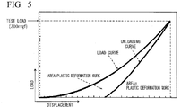
- the plastic deformation work ratio W plast /(W plast + W elast ) is shown in schematic explanation views of Figs. 4 and 5 , a load is exerted to an indentation depth of 1/10 or less of a layer thickness of the B layer (2) and the surface of the B layer (2) is displaced (see Fig. 4 ), a load curve of a displacement-load is obtained (see Fig. 5 ) and then the load is removed to obtain an unloading curve of the displacement-load (see Fig.
- a plastic deformation work ratio W plast and an elastic deformation work W elast are obtained from a difference of the load curve and the unloading curve, and the plastic deformation work ratio W plast /(W plast + W elast ) can be calculated from these values.
- a shock attenuating property is insufficient when the plastic deformation work ratio W plast /(W plast + W elast ) is less than 0.35, sufficient chipping resistance is not obtained when the (Cr, Al, M)N layer is prepared under the heavy intermittent cutting condition, plastic deformation resistance is decreased and sufficient wear resistance cannot be obtained when the plastic deformation work ratio W plast /(W plast + W elast ) exceeds 0.50. Therefore, the plastic deformation work ratio W plast /(W plast + W elast ) is 0.35 or more and 0.50 or less.
- the fact that the indentation depth is 1/10 or less of the layer thickness of the B layer (2) means that an influence on a lower layer is excluded. While a lower limit is not particularly determined, for example, it is possible to recognize a tool as the coated tool of the present invention by recognizing that the indentation depth is varied 0.1, 0.09, or 0.08 times the layer thickness of the B layer (2) and the plastic deformation work ratio W plast /(W plast + W elast ) is within a range of 0.35 or more and 0.50 or less.
- a hard coating layer is formed in an alternating laminated structure obtained by alternately laminating an A layer formed of (Ti 1-z Al z )N and a B layer formed of (Cr 1-x-y Al x M y )N at least one by one, the entire hard coating layer has excellent adhesion strength and wear resistance, a lattice constant a( ⁇ ) of crystal grains that constitute the entire hard coating layer made of the A layer and the B layer satisfies 4.10 ⁇ a ⁇ 4.20, a value of diffraction peak intensity ratio I(200)/I(111) of a (200) plane and a (111) plane satisfies 2.0 ⁇ I(200)/I(111) ⁇ 10, and further, a plastic deformation work ratio W plast /(W plast + W elast ) of the B layer of an outermost surface of the hard coating layer is within a range of 0.35 or more and 0.50 or less, excellent wear resistance is provided for
- a coated tool constituted by a tool body formed of a tungsten carbide (WC)-based cemented carbide and a coated tool constituted by a tool body formed of a cubic boron nitride (cBN) sintered material will be described as a specific example, a coated tool using a titanium carbonitride-based cermet as a tool body will also be described similarly.
- WC tungsten carbide
- cBN cubic boron nitride
- the inside of the apparatus was maintained at a temperature in the apparatus shown in Table 2, rotation was similarly suppressed to the rotation number of the rotating table (6) shown in Table 2, and when an A layer was formed, nitrogen gas was introduced into the apparatus as a reactant gas to form a predetermined reaction atmosphere within a range of 2 to 10Pa shown in Table 2, a predetermined direct current bias voltage within a range of -25 to -75V shown in Table 2 was applied to the tool body (3) that was rotated while being autorotated on the rotating table (6), and a predetermined current within a range of 90 to 140 A shown in Table 2 flowed through a cathode electrode (a vapor source) (7) for forming the A layer to generate an arc discharge.
- a cathode electrode a vapor source
- a lattice constant of crystal grains of the entire hard coating layer constituted by the A layer (1) and the B layer (2) was controlled by adjusting a bias voltage in a deposition condition of the A layer (1) and the B layer (2)
- an orientation of the crystal grains of the entire hard coating layer constituted by the A layer (1) and the B layer (2) was controlled by adjusting an arc current value, a partial pressure of nitrogen gas as the reactant gas, the bias voltage, a depositing temperature, and the like such that a hard coating layer having a lattice constant a and an X-ray diffraction peak intensity ratio I(200)/I(100) shown in Table 4 was formed.
- Fig. 3 shows an example of an X-ray diffraction result measured with respect to a hard coating layer of the tool 3 of the present invention
- a value of a ratio I(200)/I(111) of a (200) plane diffraction peak intensity I(200) and a (111) plane diffraction peak intensity I(111) of the entire hard coating layer constituted by the A layer (1) and the B layer (2) was 5.53
- a lattice constant a calculated from a (200) plane diffraction peak angle of the B layer (2) was 4.17 ⁇ .
- the coated tools (referred to as "tools of Comparative Example") 1 to 6 of Comparative Example shown in Table 5 were produced by depositing a hard coating layer having an alternating laminated structure constituted by the A layer (1) and the B layer (2) thereon.
- a composition of the A layer (1) and the B layer (2) and further a layer thickness were measured at a plurality of places through cross-sectional measurement of a longitudinal cross section of the hard coating layer using a scanning electron microscopy (SEM), a transmission electron microscope (TEM), or an energy dispersive X-ray spectroscopy (EDS), and the composition and an average layer thickness of one layer were calculated by averaging them.
- SEM scanning electron microscopy
- TEM transmission electron microscope
- EDS energy dispersive X-ray spectroscopy
- an orientation of the entire hard coating layer constituted by the A layer (1) and the B layer (2) was calculated from values of overlapping X-ray diffraction peak intensitys I(200) and I(111) of the A layer (1) and the B layer (2) measured through X-ray diffraction using a Cr bulb.
- a lattice constant of the entire hard coating layer constituted by the A layer (1) and the B layer (2) was calculated from an angle of an X-ray diffraction peak of a (200) plane (see Fig. 3 ).
- Fig. 3 shows X-ray diffraction results measured with respect to the hard coating layer of the tool 3 of the present invention.
- the B layers (2) serving as the outermost surface layers of the hard coating layers of the tools 1 to 6 of the present invention and the tools 1 to 6 of Comparative Example as produced above since a nanoindentation test is performed with an indentation depth of 1/10 or less of a layer thickness of B layer (2) (see Fig. 4 ), the surface of the B layer (2) was displaced, a load curve of a displacement-load and an unloading curve of the displacement-load were obtained (see Fig. 5 ), a plastic deformation work ratio W plast and an elastic deformation work W elast were obtained from a difference between the load curve and unloading curve, and a plastic deformation work ratio W plast /(W plast + W elast ) was calculated from these values.
- Fig. 5 shows a view schematic explaining a load curve of a displacement-load and an unloading curve of the displacement-load measured with respect to the B layer (2) of the hard coating layer of the tool 3 of the present invention. Further, a test load was determined according to a layer thickness of the tool such that an indentation depth becomes an indentation depth of 1/10 or less of the layer thickness of the B layer (2) even in a sample having the smallest layer thickness of the B layer (2) of the outermost surface in samples that are simultaneously measured. In the measurement results shown in Fig. 5 , it was confirmed that the test was performed at a test load of 200 mgf and the indentation depth was 1/10 or less of the layer thickness of the B layer (2). Various values obtained as above are shown in Table 4 and Table 5.
- Type Tool body type Cathode electrode (target) type Deposition conditions Temperatu re in apparatus (°C) Rotatin g table rotation speed (rpm) Deposition conditions upon A layer formation Deposition conditions upon B layer formation For forming A layer For forming B layer N 2 gas pressur e (Pa) Direct curren t bias voltag e (V) Arc curren t (A) N2 gas pressur e (Pa) Direct curren t bias voltag e (V) Arc curren t (A) Tools of the present inventio n 1 1 Al0.60Ti0.40 Cr0.67Al0.30Si0.03 400 1.5 6.0 -40 140 4.0 -40 120 2 2 Al0.50Ti0.50 Cr0.90Al0.05V0.05 450 3.0 2.0 -70 140 4.0 -50 140 3 3 Al0.55Ti0.45 Cr0.70Al0.30 450 2.0 6.0 -25 100 6.0 -40 100 4 1 Al0.65Ti0.35 Cr0.80Al0.20 500 1.5 10.0
- Cutting was performed to a cutting length 1600 m and a width of a flank wear was measured under the above-mentioned conditions. In addition, the existence of the occurrence of chipping was observed.
- Type Width of flank wear (mm) Existence of chipping
- Type Width of flank wear (mm) Existence of chipping Tools of the present invention 1 0.13 None Tools of Comparative example 1 *9 Exist 2 0.17 None 2 *6 Exist 3 0.09 None 3 *8 Exist 4 0.14 None 4 0.21 None 5 0.10 None 5 *6 Exist 6 0.12 None 6 *4 Exist * shows a cutting time (min) until a life time due to occurrence of chipping.
- a raw powders for forming a bonded phase of a TiN powder, a TiCN powder, an Al powder, an AlN powder, and an Al 2 O 3 powder, all of which have an average grain size of 2.0 ⁇ m or less were prepared as raw powders while preparing raw powders for forming a hard phase of cBN particles having an average grain size of 1.0 ⁇ m.
- the raw powders were blended at a blending ratio shown in Table 1 such that a content ratio of cBN particles when a content of some of the raw powders from these raw powders and a cBN powder is 100 volume % becomes 40 to 80 volume %.
- the green compact was held at a predetermined temperature within a range of 900 to 1300°C under a vacuum atmosphere of a pressure: 1Pa or less to be temporarily sintered, and then, a cBN sintered material was formed by loading the temporarily sintered material into an ultrahigh pressure sintering apparatus and sintering the temporally sintered material at a pressure: 5GPa and a predetermined temperature within a range of 1200 to 1400°C.
- the sintered material was cut to a predetermined dimension by a wire electric discharge machine, a brazing section (a corner section) of an insert main body formed of a WC-based cemented carbide having a composition of Co: 5mass%, TaC: 5mass%, WC: balance and an insert shape of ISO Standard CNGA 120408 was brazed using an Ag-based brazing filler material having a composition of Cu: 26%, Ti: 5%, Ag: balance in mass%, and cBN tool bodies 11 to 13 having an insert shape of ISO Standard CNGA 120408 were manufactured by performing grind on upper and lower surfaces and an outer circumference and honing processing.
- Tool body type Blending composition (volume %) TiN TiCN Al AlN Al 2 O 3 cBN 11 - 26 31 - 3 40 12 26 - 13 - 1 60 13 12 - 7 1 - 80
- the coated tools of the present invention shown in Table 10 (referred to as "tools of the present invention") 11 to 16 on which the hard coating layer formed in the alternating laminated structure of the A layer (1) and the B layer (2) is deposited were produced.
- an orientation and a lattice constant of the entire hard coating layer constituted by the A layer (1) and the B layer (2) were calculated from values of the measured X-ray diffraction peak intensitys I(200) and I(111).
- Example 2 the same nanoindentation test as Example 1 was performed with respect to the B layer (2), and a plastic deformation work ratio W plast /(W plast + W elast ) was calculated from the load curve of the displacement-load and the unloading curve of the displacement-load.
- Type Tool body type Cathode electrode (target) type Deposition conditions Temperatu re in apparatus (°C) Rotatin g table rotation speed (rpm) Deposition conditions upon A layer formation Deposition conditions upon B layer formation For forming A layer For forming B layer N 2 gas pressur e (Pa) Direct curren t bias voltag e (V) Arc curren t (A) N2 gas pressur e (Pa) Direct curren t bias voltag e (V) Arc curren t (A) Tools of the present inventio n 11 11 Al0.66Ti0.35 Cr0.80Al0.20 500 1.5 10.0 -25 90 10.0 -30 90 12 12 Al0.55Ti0.45 Cr0.70Al0.30 450 2.0 6.0 -25 100 6.0 -40 100 13 13 Al0.60Ti0.40 Cr0.67Al0.30Si0.03 400 1.5 6.0 -40 140 4.0 -40 120 14 11 Al0.70Ti0.3
- a dry heavy intermittent cutting test of chrome steel under the above-mentioned conditions was performed, a width of flank wear of a blade was measured, and the existence of the occurrence of chipping was observed.
- Type Width of flank wear (mm) Existence of chipping
- Type Width of flank wear (mm) Existence of chipping Tools of the present invention 11 0.09 None Tools of Comparative Example 11 *12 Exist 12 0.06 None 12 *26 Exist 13 0.09 None 13 *24 Exist 14 0.07 None 14 *19 Exist 15 0.08 None 15 0.14 None 16 0.11 None 16 *17 Exist * shows a cutting time (min) until a life time due to occurrence of chipping.
- the tools 11 to 16 of the present invention while the average of the width of the flank wear was about 0.13 mm, the tools 11 to 16 of Comparative Example had short life times due to the progression of flank wear and the occurrence of chipping over a short time.
- the tool of the present invention has excellent chipping resistance and wear resistance under heavy intermittent cutting conditions.
- a surface-coated cutting tool of the present invention provides excellent chipping resistance and wear resistance and excellent cutting performance for a long time not only in cutting under heavy intermittent cutting condition of an alloy steel but also in cutting of various workpieces such that it is possible to satisfactorily cope with high performance of a cutting apparatus, save labor of cutting, save energy and lower costs.
Landscapes
- Chemical & Material Sciences (AREA)
- Engineering & Computer Science (AREA)
- Mechanical Engineering (AREA)
- Chemical Kinetics & Catalysis (AREA)
- Materials Engineering (AREA)
- Metallurgy (AREA)
- Organic Chemistry (AREA)
- Inorganic Chemistry (AREA)
- Ceramic Engineering (AREA)
- Cutting Tools, Boring Holders, And Turrets (AREA)
- Physical Vapour Deposition (AREA)
- Drilling Tools (AREA)
Abstract
Description
- The present invention relates to a surface-coated cutting tool (hereinafter, referred to as a coated tool) showing excellent chipping resistance and wear resistance of a hard coating layer and providing excellent cutting performance for long term use in heavy intermittent cutting of an alloy steel or the like in which an intermittent and impacting heavy load is exerted to a cutting edge.
- Priority is claimed on Japanese Patent Application No.
2015-169878, filed August 29, 2015 2016-160901, filed August 18, 2016 - In general, a surface-coated cutting tool is a throwaway tip detachably attached to a tip portion of a holder and used in turning or planning of a workpiece such as various types of steel, cast iron, or the like, a drill or a miniature drill used in drilling or the like of the workpiece, a solid type end mill used in face milling, slotting, shoulder milling, or the like of the workpiece, or the like, and in addition, a throwaway end mill tool or the like, to which the throwaway tip is detachably attached, and is configured to perform cutting like the solid type end mill, which are known.
- In addition, a coated tool formed by coating a hard coating layer constituted by a complex nitride ((Cr, Al)N) layer of Cr and Al or a complex nitride ((Ti, Al)N) layer of Ti and Al on a surface of a body (hereinafter, these are generally referred to as a tool body) constituted by a tungsten carbide (hereinafter, represented by WC)-based cemented carbide, a titanium carbonitride (hereinafter, represented by TiCN)-based cermet or a cubic boron nitride sintered material (hereinafter, represented by cBN) through an arc ion plating method is used as the coated tool.
Then, in order to improve cutting performance of the coated tool, many proposals are provided. - For example, Patent Literature 1 proposes that fracture resistance of a hard coating layer in heavy cutting is improved by configuring the hard coating layer using a (Cr, Al)N layer formed of a complex nitride layer of Cr and Al satisfying a compositional formula (Cr1-XAlX)N (however, in the atomic ratio, X is 0.40 to 0.70) on a tool body surface and showing a biaxial crystal orientation in which an area ratio of crystal grains having a crystal orientation <100> within a range of 0 to 15 degrees from a normal direction of a polishing surface as a surface of the complex nitride layer is 50 % or more and further an area ratio of crystal grains having a crystal orientation <100> within a range of 15 degrees of centering on a maximum peak present within a range of 0 to 54 degrees with respect to an arbitrary orientation perpendicular to a normal line of the polishing surface as a surface of the complex nitride layer is 50 % or more when crystal orientation analysis by electron beam backward scattering diffraction (EBSD) is performed on the complex nitride layer.
- In addition,
Patent Literature 2 proposes that a life time of a coated tool can be increased by achieving a reduction in residual compressive stress while maintaining a high hardness and increasing an adhesion strength ofhard film layers 1 and 2 provided that the hard film layer 1 is coated on a side of a surface and thehard film layer 2 is coated on a side of a tool body, the hard film layer 1 is (Cr1-aAla)Nx, here, 0.5 ≤ a ≤ 0.75 and 0.9 ≤ x ≤ 1.1, thehard film layer 2 is (TibAl1-b)Ny, here, 0.4 ≤ b ≤ 0.6 and 0.9 ≤ y ≤ 1.1, when a lattice constant of a (200) plane of the hard film layer 1 in X-ray diffraction is α1 (nm), 0.411 ≤ α1 ≤ 0.415 is satisfied, and when a lattice constant of a (200) plane of thehard film layer 2 is α2 (nm), 0.413 ≤ α2 ≤ 0.418 is satisfied. - In addition,
Patent Literature 3 proposes that a life time of a coated tool can be increased by achieving a reduction in residual compressive stress while maintaining a high hardness and increasing an adhesion strength ofhard film layers 1 and 2 provided that the hard film layer 1 is coated on a side of a surface and thehard film layer 2 is coated on a side of a tool body, the hard film layer 1 is (Cr1-aAla)Nx, here, 0.5 ≤ a ≤ 0.75 and 0.9 ≤ x ≤ 1.1, thehard film layer 2 is (TibAl1-b)Ny, here, 0.4 ≤ b ≤ 0.6 and 0.9 ≤ y ≤ 1.1, and when a lattice constant of a (111) plane of the hard film layer 1 in X-ray diffraction is a1 (nm) and a lattice constant of a (111) plane of thehard film layer 2 is a2 (nm), 1.005 ≤ a2/a1 ≤ 1.025 is satisfied. - In addition,
Patent Literature 4 proposes that, in a coated tool formed by coating a (C1-XAlX)N layer (0.1 ≤ x ≤ 0.6) on a tool body surface, fracture resistance and a toughness in intermittent heavy cutting is improved provided that an area occupied by crystal grains having a particle diameter of 10 to 100 nm is 90 % or more in the measured area when (Cr1-XAlX)N crystal grains have columnar crystal structures having heights equal to an average layer thickness and a crystal grain structure in a horizontal cross section of the (Cr1-XAlX)N layer is observed and an area occupied by a division of a diameter of 0.2 to 4 µm surrounded by a crystal interface having a crstal misorientation between neighboring measurement points of 15 degrees or more is 20 % or more in an entire measured area when a crystal orientation of crystal grains of a surface is measured by an electron beam backward scattering diffraction device. - In addition, Patent Literature 5 proposes that, in a coated tool formed by coating a hard film on a tool body surface, wear resistance and oxidation resistance of the hard film are improved as the hard film is constituted by at least one element selected from an M component of Cr and Al, carbon, nitrogen, oxygen, and boron (provided that the M component is at least one element selected from 4a, 5a, and 6a family elements of the periodic table and Si, and Zr).
- Further, Patent Literature 6 proposes that lubricity and wear resistance in high-speed intermittent cutting are improved as a lower layer formed of a (Ti, Al)-based complex nitride or a complex carbonitride layer and an upper layer formed of a (Cr, Al)-based complex nitride layer are coated on a surface of a tool body, and the upper layer is configured as an alternating laminated structure of a thin layer A formed in a cubic crystal structure and a thin layer B formed in combination of a cubic crystal structure and a hexagonal crystal structure.
- Further, the lower layer is a complex nitride or a complex carbonitride layer of Ti, Al, and M1 that satisfy 0.4 ≤ Q ≤ 0.65 and 0 ≤ R ≤ 0.1 when expressed by the compositional formula: (Ti1-Q-RAlQM1R) (C, N) (here, Q is a content ratio of Al in an atomic ratio, R is a total content ratio of an component M1 with respect to the atomic ratio, and the component M1 shows one or two elements or more selected from Si, B, Zr, Y, V, W, Nb and Mo), the thin layer A is a complex nitride layer formed in a cubic crystal structure or Cr, Al, and M2 that satisfy a 0.25 ≤ α ≤ 0.65 and 0 < β ≤ 0.1 when expressed by the compositional formula: (Cr1-α-βA1αM2β)N (here, α is a content ratio of Al in an atomic ratio, β is a total content ratio of an component M2 with respect to the atomic ratio, and the component M2 shows one or two elements or more selected from Zr, Y, V, W, Nb, Mo and Ti), and further, the thin layer B is a complex nitride layer of Cr, Al, and M3 that satisfy 0.75 ≤ γ ≤ 0.95 and 0 < δ ≤ 0.1 when expressed by the compositional formula: (Cr1-γ-δAlγM3δ)N (here, y is a content ratio of Al in an atomic ratio, δ is a total content ratio of a component M3 with respect to the atomic ratio, and the component M3 shows one or two elements or more selected from Zr, Y, V, W, Nb, Mo and Ti).
-
- [Patent Literature 1] Japanese Unexamined Patent Application, First Publication No.
2008-188734 - [Patent Literature 2] Japanese Unexamined Patent Application, First Publication No.
2010-12564 - [Patent Literature 3] Japanese Unexamined Patent Application, First Publication No.
2010-284787 - [Patent Literature 4] Japanese Unexamined Patent Application, First Publication No.
2011-194535 - [Patent Literature 5] Japanese Unexamined Patent Application, First Publication No.
2006-82209 - [Patent Literature 6] Japanese Unexamined Patent Application, First Publication No.
2009-101491 - In recent years, high performance of a cutting apparatus has been remarkable, and on the other hand, there is a strong demand for labor saving and energy saving for cutting, and according to thereto, cutting tends to be highly efficient.
- In the conventional coated tools proposed in Patent Literatures 1 to 6, while there is no particular problem when the coated tools are used in cutting under a conventional condition of steel or cast iron, specifically, when the coated tools are used under a heavy intermittent cutting condition of an alloy steel in which an intermittent and impacting heavy load is exerted to a cutting edge, since chipping or the like may easily occur and wear resistance cannot also be satisfied, a lift time may be terminated after a relatively short time.
- Accordingly, from the above-mentioned viewpoint, the inventor(s) et al have earnestly studied and developed a coated tool having excellent wear resistance while providing an excellent chipping resistance of a hard coating layer in heavy intermittent cutting of alloy steel or the like in which an intermittent and impacting heavy load is exerted particularly to a cutting edge, and obtained the following knowledge.
- (a) First, in a conventional coated tool in which a hard coating layer is constituted by a (Cr, Al)N layer or a (Cr, Al, M)N layer, Al, which is a constituent of the hard coating layer, improves a high temperature hardness and thermal resistance, Cr improves high temperature strength, high temperature oxidation resistance is improved in a state in which Cr and Al are commonly contained, and properties of the hard coating layer are improved according to types of an M component such that Zr, which is an added constituent M, improves thermal plastic deformation resistance, V improves lubricity, Nb improves high temperature wear resistance, Mo improves welding resistance, W improves heat dissipation, and Ti further improves high temperature hardness, and as the hard coating layer contains these M components, fracture resistance, welding resistance, oxidation resistance and wear resistance are improved, which are already known by Patent Literatures 1 to 6.
- (b) In addition, since the (Ti, Al)N layer has excellent high temperature strength and further has excellent adhesion strength with respect to a tool body and the (Cr, Al, M)N layer, when the hard coating layer is formed as a laminated structure of an A layer and a B layer using the (Ti, Al)N layer as the A layer and the (Cr, Al, M)N layer as the B layer, the entire hard coating layer forms a coated tool having excellent high temperature strength and excellent chipping resistance, which are also already known by
Patent Literatures - (c) However, the inventor(s) has found that, in particular, as a lattice constant of crystal grains that constitute the entire hard coating layer made of the A layer and the B layer and an XRD peak intensity ratio of a (111) plane and a (200) plane of the crystal grains that constitute the hard coating layer are restricted within a predetermined range, a balance of hardness and plastic deformation provided in the B layer can be achieved, and thus, an intermittent and impacting heavy load exerted to a cutting edge during cutting can be attenuated and chipping resistance of the hard coating layer can be improved.
In addition, as a result of performing a nanoindentation test on the B layer of the present invention, it was confirmed that a value of a plastic deformation work ratio Wplast/(Wplast + Welast) was within a range of 0.35 to 0.50. - (d) Further, the inventor(s) has found that as the B layer is configured as the alternating laminated structure with the A layer, further excellent chipping resistance and wear resistance are exhibited over long term use while adhesion strength between the tool body and the hard coating layer and adhesion strength between alternately laminated layers are secured.
- The present invention was made on the basis of the above-mentioned research results and directed to aspects indicated below.
- (1) A surface-coated cutting tool comprising: a tool body made of a tungsten carbide-based cemented carbide, a titanium carbonitride-based cermet or a cubic boron nitride sintered material; and a hard coating layer provided on a surface of the tool body, the hard coating layer being made of an alternate laminate structure, in which at least each of an A layer and a B layer is laminated alternately, and having a total thickness of 0.5-3.0 µm,
- wherein (a) the A layer is a complex nitride layer of Ti and Al satisfying a compositional formula: (Ti1-zAlz)N, 0.4 ≤ z ≤ 0.7, z being a content ratio of Al in an atomic ratio,
- (b) the B layer is a complex nitride layer of Cr, Al, and M satisfying a compositional formula: (Cr1-x-yAlxMy)N, 0.03 ≤ x ≤ 0.4 and 0 ≤ y ≤ 0.05, x being a content ratio of Al in an atomic ratio, y being a total content ratio of an component M in an atomic ratio, and component M being one or more elements selected from: B, Si, and 4a, 5a, and 6a family elements of the periodic table except for Cr,
- (c) when an average layer thickness of one layer of the A layer is tA and an average layer thickness of one layer of the B layer is tB, a value of a ratio tB/tA of the average layer thickness of the one layer of the B layer with respect to the average layer thickness of the one layer of the A layer satisfies 0.67 to 2.0,
- (d) a lattice constant a(Å) of crystal grains that constitute a hard coating layer made of the A layer and the B layer calculated from a diffraction peak angle of a (200) plane obtained by X-ray diffraction of the entire hard coating layer made of the A layer and the B layer satisfies 4.10 ≤ a ≤ 4.20, and
- (e) when an X-ray diffraction peak intensity of the (200) plane is I(200) and an X-ray diffraction peak intensity of a (111) plane is I(111), each of I(200) and I(111) being obtained by the X-ray diffraction of the entire hard coating layer made of the A layer and the B layer, 2.0 ≤ I(200)/I(111) ≤ 10 is satisfied.
- (2) The surface-coated cutting tool according to (1) is characterized in that a value of a plastic deformation work ratio Wplast/(Wplast + Welast), which is obtained by performing a nanoindentation test at an indentation depth of 1/10 or less of a layer thickness of the B layer, is within a range of 0.35 to 0.50.
- Next, the coated tool of the present invention will be described in more detail.
- While
Fig. 1 shows a longitudinal cross-sectional schematic diagram of a hard coating layer of a coated tool of the present invention, since a complex nitride layer of Ti and Al that constitute an A layer (1) of the hard coating layer formed in an alternating laminated structure (hereinafter, simply referred to as "a (Ti, Al)N layer") has excellent high temperature strength and further has excellent adhesion strength with respect to both of a tool body (3) and a B layer (2), which constitutes alternating lamination, interlayer adhesion strength between the A layer and the B layer can be increased by forming the hard coating layer formed in the alternating laminated structure of the A layer (1) and the B layer (2), and as a result, chipping resistance can be improved without decreasing wear resistance. - However, when (Ti, Al)N is expressed by a compositional formula: (Ti1-zAlz)N, , wear resistance is deteriorated because a high temperature hardness is decreased when a z value (an atomic ratio) showing a content ratio of Al is less than 0.4, sufficient high temperature strength cannot be secured according to a relative reduction of a Ti content ratio and a hardness is decreased as crystal grains having a hexagonal crystal structure appear, and as a result, the wear resistance is decreased when the z value (the atomic ratio) exceeds 0.7. Therefore, the z value (the atomic ratio) showing the content ratio of Al in the A layer (1) is determined as 0.4 ≤ z ≤ 0.7.
- A complex nitride layer of Cr, Al, and M (hereinafter, referred to as "a (Cr, Al, M)N layer") that constitute the B layer (2) improves high temperature strength and improves chipping resistance of the hard coating layer according to Cr, which is a main component of the B layer (2), and contributes to improvement by of high temperature oxidation resistance by coexistent containment of Al component, and further functions as a layer of attenuating an intermittent and impacting heavy load exterted to the hard coating layer during heavy intermittent cutting.
- However, when a composition of a (Cr, Al, M)N layer is expressed by a compositional formula: (Cr1-x-yAlxMy)N, hardness is enhanced but lattice strain is increased when an x value (an atomic ratio) showing a content ratio of Al exceeds 0.4, chipping resistance is decreased,, on the other hand, the wear resistance is decreased when the x value (the atomic ratio) is less than 0.03. Therefore, the x value (the atomic ratio) is 0.03 or more and 0.4 or less.
- Meanwhile, while the M component shows one or two elements or more selected from B, Si, and 4a, 5a and 6a family elements of the periodic table except for Cr, when a y value (an atomic ratio) showing a total content ratio of the M component exceeds 0.05,, the lattice strain is increased and the chipping resistance is decreased. Therefore, the y value (the atomic ratio) is 0 ≤ y ≤ 0.05.
- Zr, Ti, V, Nb, Mo, W, B, Si, and the like, are exemplified as a specific example of the M component.
- In the components M, while Zr improves thermal plastic deformation resistance, Ti improves high temperature hardness, V improves lubricity, Nb improves high temperature wear resistance, Mo improves welding resistance, W improves heat dissipation, B improves lubricity while increasing film hardness, and Si improves thermal resistance, as described above, since the chipping resistance of the B layer (2) is decreased according to an increase in lattice strain when the y value (the atomic ratio) showing the total content ratio of the M component exceeds 0.05, an upper limit of the total content ratio of the M component is 0.05.
- While a hard coating layer having a total layer thickness of 0.5 to 3.0 µm and formed in an alternating laminated structure is configured by alternately laminating the A layer (1) and the B layer (2) at least one by one, when the average layer thickness of one layer of the A layer (1) is tA and the average layer thickness of one layer of the B layer (2) is tB, a value of a ratio tB/tA of the average layer thickness of the one layer of the B layer (2) with respect to the average layer thickness of the one layer of the A layer (1) should be 0.67 to 2.0.
- The reason for this is that, while sufficient chipping resistance cannot be obtained because a ratio of the B layer (2), which occupies the hard coating layer, is small when a layer thickness ratio tB/tA is less than 0.67, on the other hand wear resistance is decreased when the layer thickness ratio tB/tA exceeds 2.0.
- In addition, while sufficient wear resistance cannot be provided for a long time when the total layer thickness of the hard coating layer formed in the alternating laminated structure is less than 0.5 µm, the hard coating layer is prone to self-destruction when the total layer thickness exceeds 3.0 µm. Therefore, a total layer thickness of the hard coating layer is 0.5 to 3.0µm.
- Further, since adhesion strength of the tool body (3) and the hard coating layer can be secured by forming the A layer (1) directly on the surface of the tool body (3), an intermittent and shocking high load exerted during a heavy intermittent cutting can be effectively attenuated by forming the B layer (2) on the outermost surface of the hard coating layer, and further, chipping resistance can be improved, in configuring the alternating lamination formed of the A layer (1) and the B layer (2), the A layer (1) is preferably formed directly on the surface of the tool body (3) and the B layer (2) is preferably formed on the outermost surface of the hard coating layer in configuring the alternating lamination.
- Further, a composition of the A layer (1) and the B layer (2), the average layer thickness of the one layer and a total layer thickness of the hard coating layer can be measured by cross section measurement of a longitudinal cross section of the hard coating layer perpendicular to the surface of the tool body (3) using scanning electron microscopy (SEM), a transmission electron microscope (TEM), energy dispersive X-ray spectroscopy (EDS).
- In the present invention, a lattice constant a and an orientation of the crystal grains of the entire hard coating layer formed of the A layer (1) and the B layer (2) can be controlled according to a deposition condition when the A layer (1) and the B layer (2) are deposited.
- That is, while the hard coating layer is deposited using, for example, an arc ion plating apparatus (4) shown in
Figs. 2A and 2B in the present invention, the lattice constant of the crystal grains can be controlled according to a composition and a bias voltage of a target when the A layer (1) and the B layer (2) are deposited, and the orientation can be controlled by controlling an arc current value, a partial pressure of nitrogen gas serving as a reactant gas, a bias voltage, and a depositing temperature and adjusting a speed of a crystal growth and a diffusion speed of an atom. As a crystal relatively slowly grows, a (200) plane having surface energy smaller than that of a (111) plane of the crystal grains can be primarily oriented parallel to the surface of the tool body (3). - Then, provided that X-ray diffraction is performed with respect to the crystal grains that constitute the entire hard coating layer formed of the A layer (1) and the B layer (2), a diffraction peak intensity of the (200) plane is I(200) and a diffraction peak intensity of the (111) plane is I(111) while chipping resistance is decreased because the orientation of the (111) plane, which is a close-packed plane, is strong when a value of I(200)/I(111) is less than 2, and wear resistance is decreased because a (200) orientation is extremely strong when the value of I(200)/I(111) exceeds 10.
- Accordingly, in order to combine excellent chipping resistance and wear resistance, the value of I(200)/I(111) of the crystal grains that constitute the entire hard coating layer formed of the A layer (1) and the B layer (2) should be 2 or more and 10 or less.
- In addition, while a lattice constant a(Å) can be calculated from an X-ray diffraction peak angle of the (200) plane of the crystal grains of the entire hard coating layer formed of the A layer (1) and the B layer (2), since the lattice strain becomes too large and the hard coating layer is likely to be broken down during cutting when the calculated lattice constant a(Å) is less than 4.10 or more than 4.20, the lattice constant a(Å) of the crystal grains of the entire hard coating layer formed of the A layer (1) and the B layer (2) is 4.10 or more and 4.20 or less.
- While
Fig. 3 shows an example of an X-ray diffraction chart obtained by measuring the coated tool of the present invention, it should be appreciated from the chart that the value of I(200)/I(111) of the crystal grains of the entire hard coating layer formed of the A layer (1) and the B layer (2) is 2 or more and 10 or less and the lattice constant a(Å) is 4.10 or more and 4.20 or less. - It was confirmed that a nanoindentation test was performed at an indentation depth of 1/10 or less of a layer thickness of the B layer (2) in order to recognize a attenuating effect of an intermittent and impacting heavy load during cutting exhibited by the B layer (2) of the hard coating layer of the present invention, and the value was within a range of 0.35 to 0.50 in obtaining the plastic deformation work ratio Wplast/(Wplast + Welast).
- Here, the plastic deformation work ratio Wplast/(Wplast + Welast) is shown in schematic explanation views of
Figs. 4 and5 , a load is exerted to an indentation depth of 1/10 or less of a layer thickness of the B layer (2) and the surface of the B layer (2) is displaced (seeFig. 4 ), a load curve of a displacement-load is obtained (seeFig. 5 ) and then the load is removed to obtain an unloading curve of the displacement-load (seeFig. 5 ), a plastic deformation work ratio Wplast and an elastic deformation work Welast are obtained from a difference of the load curve and the unloading curve, and the plastic deformation work ratio Wplast/(Wplast + Welast) can be calculated from these values. - Then, when the plastic deformation work ratio Wplast/(Wplast + Welast) is within a range of 0.35 or more and 0.50 or less, since the B layer (2) has a shock attenuating property without decreasing plastic deformation resistance, excellent chipping resistance is provided even if the (Cr, Al, M)N layer is prepared under a heavy intermittent cutting condition.
- A shock attenuating property is insufficient when the plastic deformation work ratio Wplast/(Wplast + Welast) is less than 0.35, sufficient chipping resistance is not obtained when the (Cr, Al, M)N layer is prepared under the heavy intermittent cutting condition, plastic deformation resistance is decreased and sufficient wear resistance cannot be obtained when the plastic deformation work ratio Wplast/(Wplast + Welast) exceeds 0.50. Therefore, the plastic deformation work ratio Wplast/(Wplast + Welast) is 0.35 or more and 0.50 or less.
- Here, the fact that the indentation depth is 1/10 or less of the layer thickness of the B layer (2) means that an influence on a lower layer is excluded. While a lower limit is not particularly determined, for example, it is possible to recognize a tool as the coated tool of the present invention by recognizing that the indentation depth is varied 0.1, 0.09, or 0.08 times the layer thickness of the B layer (2) and the plastic deformation work ratio Wplast/(Wplast + Welast) is within a range of 0.35 or more and 0.50 or less.
- In a coated tool of the present invention, since a hard coating layer is formed in an alternating laminated structure obtained by alternately laminating an A layer formed of (Ti1-zAlz)N and a B layer formed of (Cr1-x-yAlxMy)N at least one by one, the entire hard coating layer has excellent adhesion strength and wear resistance, a lattice constant a(Å) of crystal grains that constitute the entire hard coating layer made of the A layer and the B layer satisfies 4.10 ≤ a ≤ 4.20, a value of diffraction peak intensity ratio I(200)/I(111) of a (200) plane and a (111) plane satisfies 2.0 ≤ I(200)/I(111) ≤ 10, and further, a plastic deformation work ratio Wplast/(Wplast + Welast) of the B layer of an outermost surface of the hard coating layer is within a range of 0.35 or more and 0.50 or less, excellent wear resistance is provided for a long time without occuring chipping or the like because the hard coating layer has an attenuation action with respect to an impact even in heavy intermittent cutting of an alloy steel or the like to which an intermittent and impacting heavy load is exerted to a cutting edge.
-
-
Fig. 1 shows an example of a longitudinal cross-sectional schematic diagram of a hard coating layer of a coated tool of the present invention. -
Fig. 2A shows a schematic plan view of an arc ion plating apparatus used in forming the hard coating layer. -
Fig. 2B shows a schematic front view of the arc ion plating apparatus used in forming the hard coating layer. -
Fig. 3 shows an example of an X-ray diffraction chart measured with respect to the coated tool of the present invention. -
Fig. 4 shows a view for schematically explaining a test method to obtain a plastic deformation work ratio. -
Fig. 5 is a view for schematically explaining a load curve of a displacement-load and an unloading curve of the displacement-load obtained by the test method ofFig. 4 . - Next, a coated tool of the present invention will be exemplarily described in detail.
- Further, while a coated tool constituted by a tool body formed of a tungsten carbide (WC)-based cemented carbide and a coated tool constituted by a tool body formed of a cubic boron nitride (cBN) sintered material will be described as a specific example, a coated tool using a titanium carbonitride-based cermet as a tool body will also be described similarly.
- A Co powder, a TiC powder, a VC powder, a TaC powder, an NbC powder, a Cr3C2 powder, and a WC powder, all of which have an average grain size of 0.5 to 5µm, were prepared as raw powders, these raw powders were blended into a blending composition shown in Table 1 and then mixed in a ball mill for 72 hours through wet mixing by adding wax, the mixed raw powders were decompressed and dried, and then the dried raw powders were pressed at a pressure of 100 MPa to sinter a green compact of these powders, and the sintered material was machined to have a predetermined dimension to form tool bodies 1 to 3 of the WC-based cemented carbide having an insert shape of ISO Standard SEEN 1203 AFTN1 were manufactured.
[Table 1] Tool body type Blending composition (mass%) Co TiC VC TaC NbC Cr3C2 WC 1 7.5 - 2.0 - 2.5 - balance 2 12.0 - 1.0 - - 0.5 balance 3 9.5 2.0 - 1.5 0.5 - balance - Using an arc ion plating apparatus (4) shown in
Figs. 2A and 2B with respect to the tool bodies 1 to 3 formed of the WC-based cemented carbide, - (a) the tool bodies 1 to 3 were mounted on an outer circumferential section at positions spaced a predetermined distance from a central axis in a radial direction on a rotating table (6) in the arc ion plating apparatus (4) in a state in which the tool bodies were ultrasonically cleaned in acetone and dried.
- (b) First, after the inside of the apparatus was heated to 500°C by a heater (5) while holding vacuum of 10-2 Pa or less by evacuating the inside of the apparatus, the inside was set to an Ar gas atmosphere of 0.5 to 2.0 Pa, a direct current bias voltage of -200 to -1000V was applied to the tool body (3) that was rotated while being autorotated on the rotating table (6), and bombarding processing was performed on a surface of the tool body (3) using argon ions for 5 to 30 minutes.
- (c) Next, a hard coating layer formed in an alternating laminated structure was formed as follows.
- First, the inside of the apparatus was maintained at a temperature in the apparatus shown in Table 2, rotation was similarly suppressed to the rotation number of the rotating table (6) shown in Table 2, and when an A layer was formed, nitrogen gas was introduced into the apparatus as a reactant gas to form a predetermined reaction atmosphere within a range of 2 to 10Pa shown in Table 2, a predetermined direct current bias voltage within a range of -25 to -75V shown in Table 2 was applied to the tool body (3) that was rotated while being autorotated on the rotating table (6), and a predetermined current within a range of 90 to 140 A shown in Table 2 flowed through a cathode electrode (a vapor source) (7) for forming the A layer to generate an arc discharge. Next, when a B layer was formed, nitrogen gas was introduced into the apparatus as the reactant gas to form a predetermined reaction atmosphere within a range of 2 to 10Pa shown in Table 2, a predetermined direct current bias voltage within a range of -25 to -75V shown in Table 2 was applied to the tool body (3) that was rotated while being autorotated on the rotating table (6), a predetermined current within a range of 90 to 140 A shown in Table 2 flowed similarly through a cathode electrode (a vapor source) (9) for forming the B layer to generate an arc discharge, and a hard coating layer formed in an alternating laminated structure having a target composition and further a target average layer thickness of one layer of the A layer (1) and the B layer (2) shown in Table 4 was deposited on surfaces of the tool bodies 1 to 3, and thus, coated tools of the present invention (referred to as "tools of the present invention") 1 to 6 shown in Table 4 were produced.
- Further, in the deposition film-forming process of (a) to (c), in particular, a lattice constant of crystal grains of the entire hard coating layer constituted by the A layer (1) and the B layer (2) was controlled by adjusting a bias voltage in a deposition condition of the A layer (1) and the B layer (2), in addition, an orientation of the crystal grains of the entire hard coating layer constituted by the A layer (1) and the B layer (2) was controlled by adjusting an arc current value, a partial pressure of nitrogen gas as the reactant gas, the bias voltage, a depositing temperature, and the like such that a hard coating layer having a lattice constant a and an X-ray diffraction peak intensity ratio I(200)/I(100) shown in Table 4 was formed.
- While
Fig. 3 shows an example of an X-ray diffraction result measured with respect to a hard coating layer of thetool 3 of the present invention, it should be appreciated that a value of a ratio I(200)/I(111) of a (200) plane diffraction peak intensity I(200) and a (111) plane diffraction peak intensity I(111) of the entire hard coating layer constituted by the A layer (1) and the B layer (2) was 5.53, and a lattice constant a calculated from a (200) plane diffraction peak angle of the B layer (2) was 4.17 Å. - For comparison, with respect to the tool bodies 1 to 3, like Example 1, under the condition shown in Table 3, the coated tools (referred to as "tools of Comparative Example") 1 to 6 of Comparative Example shown in Table 5 were produced by depositing a hard coating layer having an alternating laminated structure constituted by the A layer (1) and the B layer (2) thereon.
- In the tools 1 to 6 of the present invention and the tools 1 to 6 of Comparative Example as produced above, a composition of the A layer (1) and the B layer (2) and further a layer thickness were measured at a plurality of places through cross-sectional measurement of a longitudinal cross section of the hard coating layer using a scanning electron microscopy (SEM), a transmission electron microscope (TEM), or an energy dispersive X-ray spectroscopy (EDS), and the composition and an average layer thickness of one layer were calculated by averaging them.
- In addition, an orientation of the entire hard coating layer constituted by the A layer (1) and the B layer (2) was calculated from values of overlapping X-ray diffraction peak intensitys I(200) and I(111) of the A layer (1) and the B layer (2) measured through X-ray diffraction using a Cr bulb. In addition, a lattice constant of the entire hard coating layer constituted by the A layer (1) and the B layer (2) was calculated from an angle of an X-ray diffraction peak of a (200) plane (see
Fig. 3 ). -
Fig. 3 shows X-ray diffraction results measured with respect to the hard coating layer of thetool 3 of the present invention. - In addition, in the B layers (2) serving as the outermost surface layers of the hard coating layers of the tools 1 to 6 of the present invention and the tools 1 to 6 of Comparative Example as produced above, since a nanoindentation test is performed with an indentation depth of 1/10 or less of a layer thickness of B layer (2) (see
Fig. 4 ), the surface of the B layer (2) was displaced, a load curve of a displacement-load and an unloading curve of the displacement-load were obtained (seeFig. 5 ), a plastic deformation work ratio Wplast and an elastic deformation work Welast were obtained from a difference between the load curve and unloading curve, and a plastic deformation work ratio Wplast/(Wplast + Welast) was calculated from these values. -
Fig. 5 shows a view schematic explaining a load curve of a displacement-load and an unloading curve of the displacement-load measured with respect to the B layer (2) of the hard coating layer of thetool 3 of the present invention. Further, a test load was determined according to a layer thickness of the tool such that an indentation depth becomes an indentation depth of 1/10 or less of the layer thickness of the B layer (2) even in a sample having the smallest layer thickness of the B layer (2) of the outermost surface in samples that are simultaneously measured. In the measurement results shown inFig. 5 , it was confirmed that the test was performed at a test load of 200 mgf and the indentation depth was 1/10 or less of the layer thickness of the B layer (2). Various values obtained as above are shown in Table 4 and Table 5.[Table 2] Type Tool body type Cathode electrode (target) type Deposition conditions Temperatu re in apparatus (°C) Rotatin g table rotation speed (rpm) Deposition conditions upon A layer formation Deposition conditions upon B layer formation For forming A layer For forming B layer N2 gas pressur e (Pa) Direct curren t bias voltag e (V) Arc curren t (A) N2 gas pressur e (Pa) Direct curren t bias voltag e (V) Arc curren t (A) Tools of the present inventio n 1 1 Al0.60Ti0.40 Cr0.67Al0.30Si0.03 400 1.5 6.0 -40 140 4.0 -40 120 2 2 Al0.50Ti0.50 Cr0.90Al0.05V0.05 450 3.0 2.0 -70 140 4.0 -50 140 3 3 Al0.55Ti0.45 Cr0.70Al0.30 450 2.0 6.0 -25 100 6.0 -40 100 4 1 Al0.65Ti0.35 Cr0.80Al0.20 500 1.5 10.0 -25 90 10.0 -30 90 5 2 Al0.70Ti0.30 Cr0.79Al0.20Si0.01 500 2.0 8.0 -40 90 8.0 -50 90 6 3 Al0.45Ti0.55 Cr0.88Al0.10B0.02 400 3.0 6.0 -25 100 6.0 -26 100 [Table 3] Type Tool body type Cathode electrode (target) type Deposition conditions Temperature in apparatus (°C) Rotating table rotation speed (rpm) Deposition conditions upon A layer formation Deposition conditions upon B layer formation For forming A layer For forming B layer N2 gas pressure (Pa) Direct current bias voltage (V) Arc current (A) N2 gas pressure (Pa) Direct current bias voltage (V) Arc current (A) Tools of comparative example 1 1 Al0.5Ti0.5 Cr0.69Al0.30Si0.01 400 3.0 1.0 -50 180.0 2.0 -25 160 2 2 Al0.65Ti0.35 Cr0.55Al0.40Si0.05 350 3.0 0.5 -100 160.0 1.0 -75 160 3 3 Al0.6Ti0.4 Cr0.80Al0.20 550 1.5 10.0 -25 80.0 12.0 -100 90 4 1 Al0.7Ti0.3 Cr0.60Al0.40 450 2.0 2.0 -10 80.0 6.0 -25 160 5 2 Al0.55Ti0.45 Cr0.89Al0.10V0.01 500 1.5 14.0 -75 80.0 10.0 -100 100 6 3 Al0.45Ti0.55 Cr0.65Al0.30B0.05 350 2.0 1.0 -75 160.0 1.0 -10 140 [Table 4] Type Tool body type Hard coating layer of alternating lamination structure A layer B layer X-ray diffractio n peak intensity ratio I(200)/I( 111) Lattic e consta nt (Å) Plastic deformat ion work ratio of B layer Layer thick ness ratio (tB/t A) Total layer thick ness (µm) Layer composit ion (value of z) Average layer thickness of one layer (µm) Type of M compone nt Layer composit ion (value of x) Layer composit ion (value of y) Average layer thickness of one layer (µm) Tools of the present inventio n 1 1 0.58 0.4 Si 0.28 0.03 0.5 3.66 4.15 0.37 1.3 2.7 2 2 0.48 0.4 V 0.04 0.05 0.5 2.39 4.18 0.48 1.3 1.8 3 3 0.52 0.5 - 0.29 0.00 0.6 5.53 4.17 0.38 1.2 1.1 4 1 0.63 0.4 - 0.19 0.00 0.8 8.37 4.14 0.43 2.0 2.4 5 2 0.67 0.8 Si 0.18 0.01 0.6 7.18 4.12 0.40 0.8 1.4 6 3 0.40 0.4 B 0.09 0.02 0.4 4.24 4.19 0.45 1.0 0.8 [Table 5] Type Tool body type Hard coating layer of alternating lamination structure A layer B layer X-ray diffractio n peak intensity ratio I(200)/I( 111) Lattic e consta nt (Å) Plastic deformat ion work ratio of B layer Laye r thick ness ratio (tB/t A) Total layer thickn ess (µm) Layer composit ion (value of z) Average layer thickness of one layer (µm) Type of M compone nt Layer composit ion (value of x) Layer composit ion (value of y) Average layer thickness of one layer (µm) Tools of comparati ve example 1 1 0.48 0.5 Si 0.28 0.01 0.3 *0.96 4.17 0.36 *0.6 0.8 2 2 0.62 0.8 Si 0.37 0.04 0.7 *1.27 4.15 0.28 0.9 1.5 3 3 0.58 0.4 - 0.17 0.00 0.4 *11.4 4.17 0.39 1.0 1.6 4 1 0.68 0.5 - 0.39 0.00 0.5 2.78 *4.09 0.35 1.0 1.0 5 2 0.52 0.3 V 0.07 0.01 0.5 *12.2 *4.21 0.45 1.7 2.4 6 3 0.42 0.4 B 0.27 0.05 1.0 *1.69 4.18 0.32 *2.5 2.8 * shows items excluded from the scope claim 1 of the application. - Next, in the tools 1 to 6 of the present invention and the tools 1 to 6 of Comparative Example, a high speed face milling test of a single blade was performed under the following conditions. Cutting condition B:
- Workpiece: block material of JIS/S45C (width 70 mm × length 300 mm),
- Cutting speed: 160 m/min.,
- Rotational speed: 408 rev/min,
- Dept of cut: 2.5 mm,
- Feed: 0.20 mm/blade, and
- Width of cut: 70 mm
- Cutting was performed to a cutting length 1600 m and a width of a flank wear was measured under the above-mentioned conditions. In addition, the existence of the occurrence of chipping was observed.
- Test results are shown in Table 6.
[Table 6] Type Width of flank wear (mm) Existence of chipping Type Width of flank wear (mm) Existence of chipping Tools of the present invention 1 0.13 None Tools of Comparative example 1 *9 Exist 2 0.17 None 2 *6 Exist 3 0.09 None 3 *8 Exist 4 0.14 None 4 0.21 None 5 0.10 None 5 *6 Exist 6 0.12 None 6 *4 Exist * shows a cutting time (min) until a life time due to occurrence of chipping. - A raw powders for forming a bonded phase of a TiN powder, a TiCN powder, an Al powder, an AlN powder, and an Al2O3 powder, all of which have an average grain size of 2.0 µm or less were prepared as raw powders while preparing raw powders for forming a hard phase of cBN particles having an average grain size of 1.0 µm.
- The raw powders were blended at a blending ratio shown in Table 1 such that a content ratio of cBN particles when a content of some of the raw powders from these raw powders and a cBN powder is 100 volume % becomes 40 to 80 volume %.
- Next, after the raw powders were mixed by a ball mill for 72 hours through wet mixing and then dried, the raw powders were pressed at a dimension of a diameter: 50 mm × thickness: 1.5 mm at a molding pressure of 100 MPa, the green compact was held at a predetermined temperature within a range of 900 to 1300°C under a vacuum atmosphere of a pressure: 1Pa or less to be temporarily sintered, and then, a cBN sintered material was formed by loading the temporarily sintered material into an ultrahigh pressure sintering apparatus and sintering the temporally sintered material at a pressure: 5GPa and a predetermined temperature within a range of 1200 to 1400°C.
- The sintered material was cut to a predetermined dimension by a wire electric discharge machine, a brazing section (a corner section) of an insert main body formed of a WC-based cemented carbide having a composition of Co: 5mass%, TaC: 5mass%, WC: balance and an insert shape of ISO Standard CNGA 120408 was brazed using an Ag-based brazing filler material having a composition of Cu: 26%, Ti: 5%, Ag: balance in mass%, and cBN tool bodies 11 to 13 having an insert shape of ISO Standard CNGA 120408 were manufactured by performing grind on upper and lower surfaces and an outer circumference and honing processing.
[Table 7] Tool body type Blending composition (volume %) TiN TiCN Al AlN Al2O3 cBN 11 - 26 31 - 3 40 12 26 - 13 - 1 60 13 12 - 7 1 - 80 - Next, like the case of Example 1, as the hard coating layer is deposited on the cBN tool bodies 11 to 13 under the conditions shown in Table 8 using the arc ion plating apparatus (4) shown in
Figs. 2A and 2B , the coated tools of the present invention shown in Table 10 (referred to as "tools of the present invention") 11 to 16 on which the hard coating layer formed in the alternating laminated structure of the A layer (1) and the B layer (2) is deposited were produced. - For comparison, as the hard coating layer is deposited on the tool bodies 11 to 13 under the conditions shown in Table 9, the coated tools of Comparative Example shown in Table 11 (referred to "tools of Comparative Example) 11 to 16 were produced.
- With respect to the tools 11 to 16 of the present invention and the tools 11 to 16 of Comparative Example produced as above, like Example 1, compositions of layers and an average layer thickness of one layer were calculated.
- In addition, an orientation and a lattice constant of the entire hard coating layer constituted by the A layer (1) and the B layer (2) were calculated from values of the measured X-ray diffraction peak intensitys I(200) and I(111).
- Further, the same nanoindentation test as Example 1 was performed with respect to the B layer (2), and a plastic deformation work ratio Wplast/(Wplast + Welast) was calculated from the load curve of the displacement-load and the unloading curve of the displacement-load.
- Various values obtained as described above are shown in Tables 10 and 11.
[Table 8] Type Tool body type Cathode electrode (target) type Deposition conditions Temperatu re in apparatus (°C) Rotatin g table rotation speed (rpm) Deposition conditions upon A layer formation Deposition conditions upon B layer formation For forming A layer For forming B layer N2 gas pressur e (Pa) Direct curren t bias voltag e (V) Arc curren t (A) N2 gas pressur e (Pa) Direct curren t bias voltag e (V) Arc curren t (A) Tools of the present inventio n 11 11 Al0.66Ti0.35 Cr0.80Al0.20 500 1.5 10.0 -25 90 10.0 -30 90 12 12 Al0.55Ti0.45 Cr0.70Al0.30 450 2.0 6.0 -25 100 6.0 -40 100 13 13 Al0.60Ti0.40 Cr0.67Al0.30Si0.03 400 1.5 6.0 -40 140 4.0 -40 120 14 11 Al0.70Ti0.30 Cr0.79Al0.20Si0.01 500 2.0 8.0 -40 90 8.0 -50 90 15 12 Al0.45Ti0.55 Cr0.88Al0.10B0.02 400 3.0 6.0 -25 100 6.0 -25 100 16 13 Al0.50Ti0.50 Cr0.90Al0.05V0.05 450 3.0 2.0 -70 140 4.0 -50 140 [Table 9] Type Tool body type Cathode electrode (target) type Deposition conditions Temperature in apparatus (°C) Rotating table rotation speed (rpm) Deposition conditions upon A layer formation Deposition conditions upon B layer formation For forming A layer For forming B layer N2 gas pressure (Pa) Direct current bias voltage (V) Arc current (A) N2 gas pressure (Pa) Direct current bias voltage (V) Arc current (A) Tools of comparative example 11 11 Al0.45Ti0.55 Cr0.65Al0.30B0.05 350 2.0 1.0 -75 160.0 1.0 -10 140 12 12 Al0.6Ti0.4 Cr0.80Al0.20 550 1.5 10.0 -25 80.0 12.0 -100 90 13 13 Al0.5Ti0.5 Cr0.69Al0.30Si0.01 440 3.0 1.0 -50 180.0 2.0 -25 160 14 11 Al0.55Ti0.45 Cr0.89Al0.10V0.01 500 1.5 14.0 -75 80.0 10.0 -100 100 15 12 Al0.7Ti0.3 Cr0.60Al0.40 450 2.0 2.0 -10 80.0 6.0 -25 160 16 13 Al0.65Ti0.35 Cr0.55Al0.40Si0.05 350 3.0 0.5 -100 160.0 1.0 -75 160 [Table 10] Type Tool body type Hard coating layer of alternating lamination structure A layer B layer X-ray diffractio n peak intensity ratio I(200)/I( 111) Lattic e consta nt (Å) Plastic deformat ion work ratio of B layer Layer thick ness ratio (tB/t A) Total layer thick ness (µm) Layer composit ion (value of z) Average layer thickness of one layer (µm) Type of M compone nt Layer composit ion (value of x) Layer composit ion (value of y) Average layer thickness of one layer (µm) Tools of the present inventio n 11 11 0.62 0.4 - 0.19 0.00 0.8 8.65 4.14 0.42 2.0 2.4 12 12 0.53 0.5 - 0.28 0.00 0.6 5.36 4.17 0.39 1.2 1.1 13 13 0.58 0.4 Si 0.29 0.03 0.5 3.81 4.15 0.36 1.3 2.7 14 11 0.67 0.8 Si 0.18 0.01 0.6 7.23 4.13 0.41 0.8 1.4 15 12 0.43 0.4 B 0.10 0.02 0.4 4.32 4.19 0.44 1.0 0.8 16 13 0.47 0.4 V 0.04 0.04 0.5 2.17 4.18 0.46 1.3 1.8 [Table 11] Type Tool body type Hard coating layer of alternating lamination structure A layer B layer X-ray diffraction peak intensity ratio I(200)/I(11 1) Lattice consta nt (Å) Plastic deformati on work ratio of B layer Layer thickn ess ratio (tB/tA ) Total layer thickn ess (µm) Layer compositi on (value of z) Average layer thickness of one layer (µm) Type of M compone nt Layer compositi on (value of x) Layer compositi on (value of y) Average layer thickness of one layer (µm) Tools of comparativ e example 11 11 0.43 0.4 B 0.27 0.05 1.0 *1.87 4.19 0.31 *2.5 2.8 12 12 0.59 0.4 - 0.18 0.00 0.4 *11.2 4.16 0.41 1.0 1.6 13 13 0.47 0.5 Si 0.28 0.01 0.3 *1.43 4.17 0.37 *0.6 0.8 14 11 0.51 0.3 V 0.07 0.01 0.5 *12.1 *4.21 0.46 1.7 2.4 15 12 0.69 0.5 - 0.39 0.00 0.5 2.62 *4.09 0.36 1.0 1.0 16 13 0.63 0.8 Si 0.36 0.03 0.7 *1.36 4.15 0.29 0.9 1.5 * shows items excluded from the scope of the claim 1 of the application. - Next, in the tools 11 to 16 of the present invention and the tools 11 to 16 of Comparative Example, like the case of Example 1, the cutting test was performed under the following conditions.
- Workpiece: round bar with 8 longitudinal grooves formed equal intervals in the longitudinal direction of JIS/SCr420 (60HRC),
- Cutting speed: 130 m/min.,
- Depth of cut: 0.2 mm,
- Feed: 0.10 mm/rev.,
- Cutting time: 30 minutes.
- A dry heavy intermittent cutting test of chrome steel under the above-mentioned conditions was performed, a width of flank wear of a blade was measured, and the existence of the occurrence of chipping was observed.
- Test results are shown in Table 12.
[Table 12] Type Width of flank wear (mm) Existence of chipping Type Width of flank wear (mm) Existence of chipping Tools of the present invention 11 0.09 None Tools of Comparative Example 11 *12 Exist 12 0.06 None 12 *26 Exist 13 0.09 None 13 *24 Exist 14 0.07 None 14 *19 Exist 15 0.08 None 15 0.14 None 16 0.11 None 16 *17 Exist * shows a cutting time (min) until a life time due to occurrence of chipping. - According to the results of Table 6, in the tools 1 to 6 of the present invention, while an average of a width of a flank wear was about 0.08 mm, the tools 1 to 6 of Comparative Example had short life times due to the progression of flank wear and the occurrence of chipping over a short time.
- In addition, according to the results of Table 12, in the tools 11 to 16 of the present invention, while the average of the width of the flank wear was about 0.13 mm, the tools 11 to 16 of Comparative Example had short life times due to the progression of flank wear and the occurrence of chipping over a short time.
- From the results, it can be seen that the tool of the present invention has excellent chipping resistance and wear resistance under heavy intermittent cutting conditions.
- A surface-coated cutting tool of the present invention provides excellent chipping resistance and wear resistance and excellent cutting performance for a long time not only in cutting under heavy intermittent cutting condition of an alloy steel but also in cutting of various workpieces such that it is possible to satisfactorily cope with high performance of a cutting apparatus, save labor of cutting, save energy and lower costs.
-
- 1: A layer (Cr, Al, M)N
- 2: B layer (Ti, Al)N
- 3: Tool body
- 4: Arc ion plating apparatus
- 5: Heater
- 6: Rotating table
- 7: Cathode electrode Ti-Al alloy (vapor source)
- 8, 10: Anode electrode
- 9: Cathode electrode Cr-Al-M alloy (vapor source)
- 11: Reactant gas introduction path
- 12: Exhaust gas outlet
- 13, 14: Arc power supply
- 15: Bias power supply
Claims (2)
- A surface-coated cutting tool comprising: a tool body made of a tungsten carbide-based cemented carbide, a titanium carbonitride-based cermet or a cubic boron nitride sintered material; and a hard coating layer provided on a surface of the tool body, the hard coating layer being made of an alternate laminate structure, in which at least each of an A layer and a B layer is laminated alternately, and having a total thickness of 0.5-3.0 µm,wherein (a) the A layer is a complex nitride layer of Ti and Al satisfying a compositional formula: (Ti1-zAlz)N, 0.4 ≤ z ≤ 0.7, z being a content ratio of Al in an atomic ratio,(b) the B layer is a complex nitride layer of Cr, Al, and M satisfying a compositional formula: (Cr1-x-yAlxMy)N, 0.03 ≤ x ≤ 0.4 and 0 ≤ y ≤ 0.05, x being a content ratio of Al in an atomic ratio, y being a total content ratio of an component M in an atomic ratio, and component M being one or more elements selected from: B, Si, and 4a, 5a, and 6a family elements of the periodic table except for Cr,(c) when an average layer thickness of one layer of the A layer is tA and an average layer thickness of one layer of the B layer is tB, a value of a ratio tB/tA of the average layer thickness of the one layer of the B layer with respect to the average layer thickness of the one layer of the A layer satisfies 0.67 to 2.0,(d) a lattice constant a(Å) of crystal grains that constitute the hard coating layer made of the A layer and the B layer calculated from a diffraction peak angle of a (200) plane obtained by X-ray diffraction of the entire hard coating layer made of the A layer and the B layer satisfies 4.10 ≤ a ≤ 4.20, and(e) when an X-ray diffraction peak intensity of the (200) plane is I(200) and an X-ray diffraction peak intensity of a (111) plane is I(111), each of I(200) and I(111) being obtained by the X-ray diffraction of the entire hard coating layer made of the A layer and the B layer, 2.0 ≤ I(200)/I(111) ≤ 10 is satisfied.
- The surface-coated cutting tool according to claim 1, wherein a value of a plastic deformation work ratio Wplast/(Wplast + Wclast), which is obtained by performing a nanoindentation test at an indentation depth of 1/10 or less of a layer thickness of the B layer, is within a range of 0.35 to 0.50.
Applications Claiming Priority (3)
| Application Number | Priority Date | Filing Date | Title |
|---|---|---|---|
| JP2015169878 | 2015-08-29 | ||
| JP2016160901A JP6677932B2 (en) | 2015-08-29 | 2016-08-18 | Surface coated cutting tool that demonstrates excellent chipping and wear resistance in heavy interrupted cutting |
| PCT/JP2016/074805 WO2017038618A1 (en) | 2015-08-29 | 2016-08-25 | Surface-coated cutting tool providing excellent chipping resistance and wear resistance in strong intermittent cutting work |
Publications (3)
| Publication Number | Publication Date |
|---|---|
| EP3342512A1 true EP3342512A1 (en) | 2018-07-04 |
| EP3342512A4 EP3342512A4 (en) | 2019-03-27 |
| EP3342512B1 EP3342512B1 (en) | 2021-11-24 |
Family
ID=58209258
Family Applications (1)
| Application Number | Title | Priority Date | Filing Date |
|---|---|---|---|
| EP16841650.1A Active EP3342512B1 (en) | 2015-08-29 | 2016-08-25 | Surface-coated cutting tool providing excellent chipping resistance and wear resistance in strong intermittent cutting work |
Country Status (3)
| Country | Link |
|---|---|
| US (1) | US10927445B2 (en) |
| EP (1) | EP3342512B1 (en) |
| JP (1) | JP6677932B2 (en) |
Cited By (3)
| Publication number | Priority date | Publication date | Assignee | Title |
|---|---|---|---|---|
| KR20210143274A (en) * | 2019-05-09 | 2021-11-26 | 가부시키가이샤 몰디노 | clad cutting tool |
| EP3925720A4 (en) * | 2019-02-12 | 2022-06-29 | Mitsubishi Materials Corporation | Hard coating cutting tool |
| EP4088840A4 (en) * | 2020-01-08 | 2023-02-15 | Sumitomo Electric Hardmetal Corp. | Cutting tool |
Families Citing this family (24)
| Publication number | Priority date | Publication date | Assignee | Title |
|---|---|---|---|---|
| US10055121B2 (en) | 2015-03-07 | 2018-08-21 | Apple Inc. | Activity based thresholds and feedbacks |
| WO2017111044A1 (en) * | 2015-12-25 | 2017-06-29 | 三菱マテリアル株式会社 | Surface-coated cubic boron nitride sintered compact tool |
| JP6928218B2 (en) | 2015-12-25 | 2021-09-01 | 三菱マテリアル株式会社 | Surface-coated cubic boron nitride sintered body tool |
| JP6850980B2 (en) | 2016-03-07 | 2021-03-31 | 三菱マテリアル株式会社 | Surface-coated cubic boron nitride sintered body tool |
| WO2017154730A1 (en) * | 2016-03-07 | 2017-09-14 | 三菱マテリアル株式会社 | Surface-coated cubic boron nitride sintered tool |
| JP2018164960A (en) * | 2017-03-28 | 2018-10-25 | 三菱マテリアル株式会社 | Coated cemented carbide tool with high fracture resistance |
| US11192189B2 (en) | 2017-05-30 | 2021-12-07 | Kyocera Corporation | Coated tool and cutting tool including same |
| JP6635347B2 (en) * | 2017-06-27 | 2020-01-22 | 株式会社タンガロイ | Coated cutting tool |
| JPWO2019044715A1 (en) | 2017-08-29 | 2020-09-17 | 京セラ株式会社 | Covering tool and cutting tool equipped with it |
| JPWO2019044714A1 (en) | 2017-08-29 | 2020-09-17 | 京セラ株式会社 | Covering tool and cutting tool equipped with it |
| KR102064172B1 (en) * | 2017-09-01 | 2020-01-09 | 한국야금 주식회사 | Hard film having excellent wear resistance and toughness |
| KR102343013B1 (en) | 2017-09-27 | 2021-12-24 | 교세라 가부시키가이샤 | Covered tool and cutting tool having same |
| KR102343014B1 (en) | 2017-09-27 | 2021-12-24 | 교세라 가부시키가이샤 | Covered tool and cutting tool having same |
| JP7165594B2 (en) * | 2019-02-07 | 2022-11-04 | 京セラ株式会社 | Coated tool and cutting tool with the same |
| JP7216914B2 (en) * | 2019-03-12 | 2023-02-02 | 三菱マテリアル株式会社 | A surface-coated cutting tool that exhibits excellent chipping resistance and wear resistance in high-load cutting. |
| JP7195410B2 (en) * | 2019-03-27 | 2022-12-23 | 京セラ株式会社 | Coated tool and cutting tool with the same |
| DE102019113117B4 (en) * | 2019-05-17 | 2023-12-28 | voestalpine eifeler Vacotec GmbH | Method for producing a cold forming tool and cold forming tool |
| JP7415223B2 (en) * | 2020-02-14 | 2024-01-17 | 三菱マテリアル株式会社 | A surface-coated cutting tool that exhibits excellent chipping and wear resistance during heavy interrupted cutting. |
| JP7795453B2 (en) * | 2020-03-27 | 2026-01-07 | 京セラ株式会社 | Coated and cutting tools |
| JP7108966B2 (en) * | 2020-06-24 | 2022-07-29 | 株式会社タンガロイ | coated cutting tools |
| JP7507887B2 (en) * | 2020-12-25 | 2024-06-28 | 京セラ株式会社 | Coated and cutting tools |
| WO2022180093A1 (en) * | 2021-02-23 | 2022-09-01 | Oerlikon Surface Solutions Ag, Pfäffikon | Coating system for plastic processing applications |
| CN115418607B (en) * | 2022-08-25 | 2024-02-23 | 株洲钻石切削刀具股份有限公司 | Composite coated cutting tool containing chromium oxide layer |
| CN116180006B (en) * | 2023-02-08 | 2024-05-03 | 苏州六九新材料科技有限公司 | TiAlN/CrAlLaBN composite coating, preparation method thereof and cutter |
Family Cites Families (16)
| Publication number | Priority date | Publication date | Assignee | Title |
|---|---|---|---|---|
| JP3598074B2 (en) * | 2001-05-11 | 2004-12-08 | 日立ツール株式会社 | Hard coating tool |
| JP4453902B2 (en) * | 2004-02-12 | 2010-04-21 | 日立ツール株式会社 | Hard coating and hard coating tool |
| US7368182B2 (en) * | 2004-02-12 | 2008-05-06 | Hitachi Tool Engineering, Ltd. | Hard coating and its formation method, and hard-coated tool |
| JP2006082209A (en) | 2004-09-17 | 2006-03-30 | Sumitomo Electric Hardmetal Corp | Surface coated cutting tool |
| WO2006070509A1 (en) | 2004-12-28 | 2006-07-06 | Sumitomo Electric Hardmetal Corp. | Surface-coated cutting tool and process for producing the same |
| JP5036338B2 (en) | 2007-02-06 | 2012-09-26 | 三菱マテリアル株式会社 | Surface-coated cutting tool with excellent fracture resistance due to hard coating layer |
| JP2009101491A (en) | 2007-10-25 | 2009-05-14 | Mitsubishi Materials Corp | Surface coated cutting tool with excellent lubricity and wear resistance with high hard coating layer in high speed cutting |
| JP5206167B2 (en) | 2008-07-04 | 2013-06-12 | 日立ツール株式会社 | Hard film coated cutting tool |
| JP2010284787A (en) | 2009-06-15 | 2010-12-24 | Hitachi Tool Engineering Ltd | Hard film coated cutting tool |
| JP5560513B2 (en) | 2010-03-23 | 2014-07-30 | 三菱マテリアル株式会社 | Surface-coated cutting tool with excellent fracture resistance due to hard coating layer |
| JP5010707B2 (en) * | 2010-04-13 | 2012-08-29 | ユニオンツール株式会社 | Hard coating for cutting tools |
| JP5730535B2 (en) * | 2010-10-29 | 2015-06-10 | 株式会社神戸製鋼所 | Hard film forming member and hard film forming method |
| KR101351843B1 (en) * | 2012-05-02 | 2014-01-16 | 한국야금 주식회사 | Hard coating film for cutting tools |
| JP6011249B2 (en) * | 2012-10-31 | 2016-10-19 | 三菱マテリアル株式会社 | Surface coated cutting tool |
| US9896767B2 (en) * | 2013-08-16 | 2018-02-20 | Kennametal Inc | Low stress hard coatings and applications thereof |
| US9168664B2 (en) * | 2013-08-16 | 2015-10-27 | Kennametal Inc. | Low stress hard coatings and applications thereof |
-
2016
- 2016-08-18 JP JP2016160901A patent/JP6677932B2/en active Active
- 2016-08-25 EP EP16841650.1A patent/EP3342512B1/en active Active
- 2016-08-25 US US15/755,982 patent/US10927445B2/en active Active
Cited By (9)
| Publication number | Priority date | Publication date | Assignee | Title |
|---|---|---|---|---|
| EP3925720A4 (en) * | 2019-02-12 | 2022-06-29 | Mitsubishi Materials Corporation | Hard coating cutting tool |
| US12303982B2 (en) | 2019-02-12 | 2025-05-20 | Mitsubishi Materials Corporation | Surface-coated cutting tool |
| KR20210143274A (en) * | 2019-05-09 | 2021-11-26 | 가부시키가이샤 몰디노 | clad cutting tool |
| CN113874143A (en) * | 2019-05-09 | 2021-12-31 | 株式会社Moldino | Coated cutting tool |
| EP3967430A4 (en) * | 2019-05-09 | 2022-08-31 | MOLDINO Tool Engineering, Ltd. | Coated cutting tool |
| US11965235B2 (en) | 2019-05-09 | 2024-04-23 | Moldino Tool Engineering, Ltd. | Coated cutting tool |
| CN113874143B (en) * | 2019-05-09 | 2024-09-27 | 株式会社Moldino | Coated cutting tools |
| EP4088840A4 (en) * | 2020-01-08 | 2023-02-15 | Sumitomo Electric Hardmetal Corp. | Cutting tool |
| US12370606B2 (en) | 2020-01-08 | 2025-07-29 | Sumitomo Electric Hardmetal Corp. | Cutting tool |
Also Published As
| Publication number | Publication date |
|---|---|
| JP2017042906A (en) | 2017-03-02 |
| EP3342512A4 (en) | 2019-03-27 |
| EP3342512B1 (en) | 2021-11-24 |
| JP6677932B2 (en) | 2020-04-08 |
| US10927445B2 (en) | 2021-02-23 |
| US20190040519A1 (en) | 2019-02-07 |
Similar Documents
| Publication | Publication Date | Title |
|---|---|---|
| EP3342512B1 (en) | Surface-coated cutting tool providing excellent chipping resistance and wear resistance in strong intermittent cutting work | |
| EP2823923B1 (en) | Surface-coated cutting tool having therein hard coating layer capable of exhibiting excellent chipping resistance during high-speed intermittent cutting work | |
| EP3225337B1 (en) | Surface-coated cutting tool with excellent chipping resistance and wear resistance | |
| EP1867754B1 (en) | Cutting tool made of surface-coated cubic boron nitride-based ultra-high-pressure sintered material | |
| EP3427872B1 (en) | Surface-coated cubic boron nitride sintered tool | |
| JP5838769B2 (en) | Surface coated cutting tool | |
| EP3202515A1 (en) | Surface-coated cutting tool having excellent chip resistance | |
| EP3395484B1 (en) | Surface-coated cubic boron nitride sintered compact tool | |
| JP5207109B2 (en) | Surface-coated cutting tool with excellent fracture resistance due to hard coating layer | |
| JP2021126738A (en) | Surface coating cutting tool that demonstrates excellent chipping resistance and wear resistance in strong intermittent cutting | |
| JP6296295B2 (en) | Surface coated cutting tool with excellent wear resistance | |
| EP3219420B1 (en) | Surface-coated cutting tool | |
| JP5287124B2 (en) | Surface-coated cutting tool with excellent fracture resistance due to hard coating layer | |
| JP2008254159A (en) | Cutting tool made of surface coated cubic boron nitride based ultra high pressure sintered material | |
| JP4780513B2 (en) | Surface coated cermet cutting tool whose hard coating layer exhibits excellent chipping resistance in high speed cutting | |
| JP4807575B2 (en) | Cutting tool made of surface-coated cubic boron nitride-based ultra-high pressure sintered material that exhibits excellent wear resistance in high-speed cutting of hardened steel | |
| JP5945162B2 (en) | Surface coated cutting tool | |
| JP5099587B2 (en) | Surface-coated cutting tool with excellent fracture resistance due to hard coating layer | |
| JP2016064470A (en) | Surface coated cutting tool with excellent chipping resistance and wear resistance | |
| WO2017154730A1 (en) | Surface-coated cubic boron nitride sintered tool | |
| JP4883471B2 (en) | Cutting tool made of surface-coated cubic boron nitride-based ultra-high pressure sintered material that exhibits excellent chipping resistance in hard cutting of hardened steel | |
| JP6471546B2 (en) | Surface coated cutting tool | |
| WO2017038618A1 (en) | Surface-coated cutting tool providing excellent chipping resistance and wear resistance in strong intermittent cutting work | |
| JP4857950B2 (en) | Surface coated cermet cutting tool whose hard coating layer exhibits excellent chipping resistance and wear resistance in high-speed intermittent cutting | |
| JP4748445B2 (en) | Cutting tool made of super-high-pressure sintered material with surface-coated cubic boron nitride that exhibits excellent chipping resistance with a hard coating layer in intermittent cutting of high-hardness steel |
Legal Events
| Date | Code | Title | Description |
|---|---|---|---|
| STAA | Information on the status of an ep patent application or granted ep patent |
Free format text: STATUS: THE INTERNATIONAL PUBLICATION HAS BEEN MADE |
|
| PUAI | Public reference made under article 153(3) epc to a published international application that has entered the european phase |
Free format text: ORIGINAL CODE: 0009012 |
|
| STAA | Information on the status of an ep patent application or granted ep patent |
Free format text: STATUS: REQUEST FOR EXAMINATION WAS MADE |
|
| 17P | Request for examination filed |
Effective date: 20180306 |
|
| AK | Designated contracting states |
Kind code of ref document: A1 Designated state(s): AL AT BE BG CH CY CZ DE DK EE ES FI FR GB GR HR HU IE IS IT LI LT LU LV MC MK MT NL NO PL PT RO RS SE SI SK SM TR |
|
| AX | Request for extension of the european patent |
Extension state: BA ME |
|
| DAV | Request for validation of the european patent (deleted) | ||
| DAX | Request for extension of the european patent (deleted) | ||
| A4 | Supplementary search report drawn up and despatched |
Effective date: 20190222 |
|
| RIC1 | Information provided on ipc code assigned before grant |
Ipc: B23C 5/16 20060101ALI20190215BHEP Ipc: C23C 14/06 20060101ALI20190215BHEP Ipc: B23B 27/14 20060101AFI20190215BHEP Ipc: B23B 51/00 20060101ALI20190215BHEP Ipc: C23C 14/48 20060101ALI20190215BHEP |
|
| RAP1 | Party data changed (applicant data changed or rights of an application transferred) |
Owner name: MITSUBISHI MATERIALS CORPORATION |
|
| GRAP | Despatch of communication of intention to grant a patent |
Free format text: ORIGINAL CODE: EPIDOSNIGR1 |
|
| STAA | Information on the status of an ep patent application or granted ep patent |
Free format text: STATUS: GRANT OF PATENT IS INTENDED |
|
| RIC1 | Information provided on ipc code assigned before grant |
Ipc: B23B 27/14 20060101AFI20210706BHEP Ipc: B23B 51/00 20060101ALI20210706BHEP Ipc: B23C 5/16 20060101ALI20210706BHEP Ipc: C23C 14/06 20060101ALI20210706BHEP Ipc: C23C 14/48 20060101ALI20210706BHEP Ipc: C23C 14/32 20060101ALI20210706BHEP Ipc: C23C 28/04 20060101ALI20210706BHEP |
|
| INTG | Intention to grant announced |
Effective date: 20210730 |
|
| GRAS | Grant fee paid |
Free format text: ORIGINAL CODE: EPIDOSNIGR3 |
|
| GRAA | (expected) grant |
Free format text: ORIGINAL CODE: 0009210 |
|
| STAA | Information on the status of an ep patent application or granted ep patent |
Free format text: STATUS: THE PATENT HAS BEEN GRANTED |
|
| AK | Designated contracting states |
Kind code of ref document: B1 Designated state(s): AL AT BE BG CH CY CZ DE DK EE ES FI FR GB GR HR HU IE IS IT LI LT LU LV MC MK MT NL NO PL PT RO RS SE SI SK SM TR |
|
| REG | Reference to a national code |
Ref country code: GB Ref legal event code: FG4D |
|
| REG | Reference to a national code |
Ref country code: AT Ref legal event code: REF Ref document number: 1449466 Country of ref document: AT Kind code of ref document: T Effective date: 20211215 |
|
| REG | Reference to a national code |
Ref country code: DE Ref legal event code: R096 Ref document number: 602016066652 Country of ref document: DE |
|
| REG | Reference to a national code |
Ref country code: IE Ref legal event code: FG4D |
|
| REG | Reference to a national code |
Ref country code: LT Ref legal event code: MG9D |
|
| REG | Reference to a national code |
Ref country code: NL Ref legal event code: MP Effective date: 20211124 |
|
| REG | Reference to a national code |
Ref country code: AT Ref legal event code: MK05 Ref document number: 1449466 Country of ref document: AT Kind code of ref document: T Effective date: 20211124 |
|
| PG25 | Lapsed in a contracting state [announced via postgrant information from national office to epo] |
Ref country code: RS Free format text: LAPSE BECAUSE OF FAILURE TO SUBMIT A TRANSLATION OF THE DESCRIPTION OR TO PAY THE FEE WITHIN THE PRESCRIBED TIME-LIMIT Effective date: 20211124 Ref country code: LT Free format text: LAPSE BECAUSE OF FAILURE TO SUBMIT A TRANSLATION OF THE DESCRIPTION OR TO PAY THE FEE WITHIN THE PRESCRIBED TIME-LIMIT Effective date: 20211124 Ref country code: FI Free format text: LAPSE BECAUSE OF FAILURE TO SUBMIT A TRANSLATION OF THE DESCRIPTION OR TO PAY THE FEE WITHIN THE PRESCRIBED TIME-LIMIT Effective date: 20211124 Ref country code: BG Free format text: LAPSE BECAUSE OF FAILURE TO SUBMIT A TRANSLATION OF THE DESCRIPTION OR TO PAY THE FEE WITHIN THE PRESCRIBED TIME-LIMIT Effective date: 20220224 Ref country code: AT Free format text: LAPSE BECAUSE OF FAILURE TO SUBMIT A TRANSLATION OF THE DESCRIPTION OR TO PAY THE FEE WITHIN THE PRESCRIBED TIME-LIMIT Effective date: 20211124 |
|
| PG25 | Lapsed in a contracting state [announced via postgrant information from national office to epo] |
Ref country code: IS Free format text: LAPSE BECAUSE OF FAILURE TO SUBMIT A TRANSLATION OF THE DESCRIPTION OR TO PAY THE FEE WITHIN THE PRESCRIBED TIME-LIMIT Effective date: 20220324 Ref country code: SE Free format text: LAPSE BECAUSE OF FAILURE TO SUBMIT A TRANSLATION OF THE DESCRIPTION OR TO PAY THE FEE WITHIN THE PRESCRIBED TIME-LIMIT Effective date: 20211124 Ref country code: PT Free format text: LAPSE BECAUSE OF FAILURE TO SUBMIT A TRANSLATION OF THE DESCRIPTION OR TO PAY THE FEE WITHIN THE PRESCRIBED TIME-LIMIT Effective date: 20220324 Ref country code: PL Free format text: LAPSE BECAUSE OF FAILURE TO SUBMIT A TRANSLATION OF THE DESCRIPTION OR TO PAY THE FEE WITHIN THE PRESCRIBED TIME-LIMIT Effective date: 20211124 Ref country code: NO Free format text: LAPSE BECAUSE OF FAILURE TO SUBMIT A TRANSLATION OF THE DESCRIPTION OR TO PAY THE FEE WITHIN THE PRESCRIBED TIME-LIMIT Effective date: 20220224 Ref country code: NL Free format text: LAPSE BECAUSE OF FAILURE TO SUBMIT A TRANSLATION OF THE DESCRIPTION OR TO PAY THE FEE WITHIN THE PRESCRIBED TIME-LIMIT Effective date: 20211124 Ref country code: LV Free format text: LAPSE BECAUSE OF FAILURE TO SUBMIT A TRANSLATION OF THE DESCRIPTION OR TO PAY THE FEE WITHIN THE PRESCRIBED TIME-LIMIT Effective date: 20211124 Ref country code: HR Free format text: LAPSE BECAUSE OF FAILURE TO SUBMIT A TRANSLATION OF THE DESCRIPTION OR TO PAY THE FEE WITHIN THE PRESCRIBED TIME-LIMIT Effective date: 20211124 Ref country code: GR Free format text: LAPSE BECAUSE OF FAILURE TO SUBMIT A TRANSLATION OF THE DESCRIPTION OR TO PAY THE FEE WITHIN THE PRESCRIBED TIME-LIMIT Effective date: 20220225 Ref country code: ES Free format text: LAPSE BECAUSE OF FAILURE TO SUBMIT A TRANSLATION OF THE DESCRIPTION OR TO PAY THE FEE WITHIN THE PRESCRIBED TIME-LIMIT Effective date: 20211124 |
|
| PG25 | Lapsed in a contracting state [announced via postgrant information from national office to epo] |
Ref country code: SM Free format text: LAPSE BECAUSE OF FAILURE TO SUBMIT A TRANSLATION OF THE DESCRIPTION OR TO PAY THE FEE WITHIN THE PRESCRIBED TIME-LIMIT Effective date: 20211124 Ref country code: SK Free format text: LAPSE BECAUSE OF FAILURE TO SUBMIT A TRANSLATION OF THE DESCRIPTION OR TO PAY THE FEE WITHIN THE PRESCRIBED TIME-LIMIT Effective date: 20211124 Ref country code: RO Free format text: LAPSE BECAUSE OF FAILURE TO SUBMIT A TRANSLATION OF THE DESCRIPTION OR TO PAY THE FEE WITHIN THE PRESCRIBED TIME-LIMIT Effective date: 20211124 Ref country code: EE Free format text: LAPSE BECAUSE OF FAILURE TO SUBMIT A TRANSLATION OF THE DESCRIPTION OR TO PAY THE FEE WITHIN THE PRESCRIBED TIME-LIMIT Effective date: 20211124 Ref country code: DK Free format text: LAPSE BECAUSE OF FAILURE TO SUBMIT A TRANSLATION OF THE DESCRIPTION OR TO PAY THE FEE WITHIN THE PRESCRIBED TIME-LIMIT Effective date: 20211124 Ref country code: CZ Free format text: LAPSE BECAUSE OF FAILURE TO SUBMIT A TRANSLATION OF THE DESCRIPTION OR TO PAY THE FEE WITHIN THE PRESCRIBED TIME-LIMIT Effective date: 20211124 |
|
| REG | Reference to a national code |
Ref country code: DE Ref legal event code: R097 Ref document number: 602016066652 Country of ref document: DE |
|
| PLBE | No opposition filed within time limit |
Free format text: ORIGINAL CODE: 0009261 |
|
| STAA | Information on the status of an ep patent application or granted ep patent |
Free format text: STATUS: NO OPPOSITION FILED WITHIN TIME LIMIT |
|
| PG25 | Lapsed in a contracting state [announced via postgrant information from national office to epo] |
Ref country code: AL Free format text: LAPSE BECAUSE OF FAILURE TO SUBMIT A TRANSLATION OF THE DESCRIPTION OR TO PAY THE FEE WITHIN THE PRESCRIBED TIME-LIMIT Effective date: 20211124 |
|
| 26N | No opposition filed |
Effective date: 20220825 |
|
| PG25 | Lapsed in a contracting state [announced via postgrant information from national office to epo] |
Ref country code: SI Free format text: LAPSE BECAUSE OF FAILURE TO SUBMIT A TRANSLATION OF THE DESCRIPTION OR TO PAY THE FEE WITHIN THE PRESCRIBED TIME-LIMIT Effective date: 20211124 |
|
| PG25 | Lapsed in a contracting state [announced via postgrant information from national office to epo] |
Ref country code: MC Free format text: LAPSE BECAUSE OF FAILURE TO SUBMIT A TRANSLATION OF THE DESCRIPTION OR TO PAY THE FEE WITHIN THE PRESCRIBED TIME-LIMIT Effective date: 20211124 |
|
| REG | Reference to a national code |
Ref country code: CH Ref legal event code: PL |
|
| GBPC | Gb: european patent ceased through non-payment of renewal fee |
Effective date: 20220825 |
|
| PG25 | Lapsed in a contracting state [announced via postgrant information from national office to epo] |
Ref country code: LU Free format text: LAPSE BECAUSE OF NON-PAYMENT OF DUE FEES Effective date: 20220825 Ref country code: LI Free format text: LAPSE BECAUSE OF NON-PAYMENT OF DUE FEES Effective date: 20220831 Ref country code: CH Free format text: LAPSE BECAUSE OF NON-PAYMENT OF DUE FEES Effective date: 20220831 |
|
| REG | Reference to a national code |
Ref country code: BE Ref legal event code: MM Effective date: 20220831 |
|
| PG25 | Lapsed in a contracting state [announced via postgrant information from national office to epo] |
Ref country code: IT Free format text: LAPSE BECAUSE OF FAILURE TO SUBMIT A TRANSLATION OF THE DESCRIPTION OR TO PAY THE FEE WITHIN THE PRESCRIBED TIME-LIMIT Effective date: 20211124 |
|
| PG25 | Lapsed in a contracting state [announced via postgrant information from national office to epo] |
Ref country code: IE Free format text: LAPSE BECAUSE OF NON-PAYMENT OF DUE FEES Effective date: 20220825 Ref country code: FR Free format text: LAPSE BECAUSE OF NON-PAYMENT OF DUE FEES Effective date: 20220831 |
|
| PG25 | Lapsed in a contracting state [announced via postgrant information from national office to epo] |
Ref country code: BE Free format text: LAPSE BECAUSE OF NON-PAYMENT OF DUE FEES Effective date: 20220831 |
|
| PG25 | Lapsed in a contracting state [announced via postgrant information from national office to epo] |
Ref country code: GB Free format text: LAPSE BECAUSE OF NON-PAYMENT OF DUE FEES Effective date: 20220825 |
|
| PG25 | Lapsed in a contracting state [announced via postgrant information from national office to epo] |
Ref country code: HU Free format text: LAPSE BECAUSE OF FAILURE TO SUBMIT A TRANSLATION OF THE DESCRIPTION OR TO PAY THE FEE WITHIN THE PRESCRIBED TIME-LIMIT; INVALID AB INITIO Effective date: 20160825 |
|
| PG25 | Lapsed in a contracting state [announced via postgrant information from national office to epo] |
Ref country code: CY Free format text: LAPSE BECAUSE OF FAILURE TO SUBMIT A TRANSLATION OF THE DESCRIPTION OR TO PAY THE FEE WITHIN THE PRESCRIBED TIME-LIMIT Effective date: 20211124 |
|
| PG25 | Lapsed in a contracting state [announced via postgrant information from national office to epo] |
Ref country code: MK Free format text: LAPSE BECAUSE OF FAILURE TO SUBMIT A TRANSLATION OF THE DESCRIPTION OR TO PAY THE FEE WITHIN THE PRESCRIBED TIME-LIMIT Effective date: 20211124 |
|
| PG25 | Lapsed in a contracting state [announced via postgrant information from national office to epo] |
Ref country code: MT Free format text: LAPSE BECAUSE OF FAILURE TO SUBMIT A TRANSLATION OF THE DESCRIPTION OR TO PAY THE FEE WITHIN THE PRESCRIBED TIME-LIMIT Effective date: 20211124 |
|
| PGFP | Annual fee paid to national office [announced via postgrant information from national office to epo] |
Ref country code: DE Payment date: 20250820 Year of fee payment: 10 |
|
| PG25 | Lapsed in a contracting state [announced via postgrant information from national office to epo] |
Ref country code: TR Free format text: LAPSE BECAUSE OF FAILURE TO SUBMIT A TRANSLATION OF THE DESCRIPTION OR TO PAY THE FEE WITHIN THE PRESCRIBED TIME-LIMIT Effective date: 20211124 |