EP3342047B1 - Dynamically configurable apparatus for operating within the current capabilities of the power source - Google Patents
Dynamically configurable apparatus for operating within the current capabilities of the power source Download PDFInfo
- Publication number
- EP3342047B1 EP3342047B1 EP16742135.3A EP16742135A EP3342047B1 EP 3342047 B1 EP3342047 B1 EP 3342047B1 EP 16742135 A EP16742135 A EP 16742135A EP 3342047 B1 EP3342047 B1 EP 3342047B1
- Authority
- EP
- European Patent Office
- Prior art keywords
- load
- current
- power source
- power
- current limiting
- Prior art date
- Legal status (The legal status is an assumption and is not a legal conclusion. Google has not performed a legal analysis and makes no representation as to the accuracy of the status listed.)
- Active
Links
- 238000004891 communication Methods 0.000 claims description 55
- 238000000034 method Methods 0.000 description 18
- 238000010586 diagram Methods 0.000 description 14
- 230000000116 mitigating effect Effects 0.000 description 12
- 238000013461 design Methods 0.000 description 5
- 230000008569 process Effects 0.000 description 5
- 239000013256 coordination polymer Substances 0.000 description 4
- 238000005516 engineering process Methods 0.000 description 4
- 230000006870 function Effects 0.000 description 4
- 239000007795 chemical reaction product Substances 0.000 description 3
- 230000008878 coupling Effects 0.000 description 3
- 238000010168 coupling process Methods 0.000 description 3
- 238000005859 coupling reaction Methods 0.000 description 3
- 239000013067 intermediate product Substances 0.000 description 3
- 230000002776 aggregation Effects 0.000 description 2
- 238000004220 aggregation Methods 0.000 description 2
- 230000008901 benefit Effects 0.000 description 2
- 230000005540 biological transmission Effects 0.000 description 2
- 230000004048 modification Effects 0.000 description 2
- 238000012986 modification Methods 0.000 description 2
- 238000013459 approach Methods 0.000 description 1
- 238000003491 array Methods 0.000 description 1
- 230000001413 cellular effect Effects 0.000 description 1
- 230000001276 controlling effect Effects 0.000 description 1
- 230000007423 decrease Effects 0.000 description 1
- 230000003247 decreasing effect Effects 0.000 description 1
- 230000001419 dependent effect Effects 0.000 description 1
- 230000007774 longterm Effects 0.000 description 1
- 238000010295 mobile communication Methods 0.000 description 1
- 230000001105 regulatory effect Effects 0.000 description 1
Images


Classifications
-
- G—PHYSICS
- G06—COMPUTING; CALCULATING OR COUNTING
- G06F—ELECTRIC DIGITAL DATA PROCESSING
- G06F1/00—Details not covered by groups G06F3/00 - G06F13/00 and G06F21/00
- G06F1/26—Power supply means, e.g. regulation thereof
- G06F1/32—Means for saving power
- G06F1/3203—Power management, i.e. event-based initiation of a power-saving mode
- G06F1/3234—Power saving characterised by the action undertaken
- G06F1/3243—Power saving in microcontroller unit
-
- H—ELECTRICITY
- H04—ELECTRIC COMMUNICATION TECHNIQUE
- H04W—WIRELESS COMMUNICATION NETWORKS
- H04W52/00—Power management, e.g. TPC [Transmission Power Control], power saving or power classes
- H04W52/02—Power saving arrangements
- H04W52/0209—Power saving arrangements in terminal devices
- H04W52/0261—Power saving arrangements in terminal devices managing power supply demand, e.g. depending on battery level
- H04W52/0274—Power saving arrangements in terminal devices managing power supply demand, e.g. depending on battery level by switching on or off the equipment or parts thereof
- H04W52/0277—Power saving arrangements in terminal devices managing power supply demand, e.g. depending on battery level by switching on or off the equipment or parts thereof according to available power supply, e.g. switching off when a low battery condition is detected
-
- H—ELECTRICITY
- H04—ELECTRIC COMMUNICATION TECHNIQUE
- H04W—WIRELESS COMMUNICATION NETWORKS
- H04W52/00—Power management, e.g. TPC [Transmission Power Control], power saving or power classes
- H04W52/02—Power saving arrangements
- H04W52/0209—Power saving arrangements in terminal devices
- H04W52/0261—Power saving arrangements in terminal devices managing power supply demand, e.g. depending on battery level
- H04W52/0274—Power saving arrangements in terminal devices managing power supply demand, e.g. depending on battery level by switching on or off the equipment or parts thereof
- H04W52/028—Power saving arrangements in terminal devices managing power supply demand, e.g. depending on battery level by switching on or off the equipment or parts thereof switching on or off only a part of the equipment circuit blocks
-
- H—ELECTRICITY
- H04—ELECTRIC COMMUNICATION TECHNIQUE
- H04W—WIRELESS COMMUNICATION NETWORKS
- H04W52/00—Power management, e.g. TPC [Transmission Power Control], power saving or power classes
- H04W52/04—TPC
- H04W52/38—TPC being performed in particular situations
-
- Y—GENERAL TAGGING OF NEW TECHNOLOGICAL DEVELOPMENTS; GENERAL TAGGING OF CROSS-SECTIONAL TECHNOLOGIES SPANNING OVER SEVERAL SECTIONS OF THE IPC; TECHNICAL SUBJECTS COVERED BY FORMER USPC CROSS-REFERENCE ART COLLECTIONS [XRACs] AND DIGESTS
- Y02—TECHNOLOGIES OR APPLICATIONS FOR MITIGATION OR ADAPTATION AGAINST CLIMATE CHANGE
- Y02D—CLIMATE CHANGE MITIGATION TECHNOLOGIES IN INFORMATION AND COMMUNICATION TECHNOLOGIES [ICT], I.E. INFORMATION AND COMMUNICATION TECHNOLOGIES AIMING AT THE REDUCTION OF THEIR OWN ENERGY USE
- Y02D30/00—Reducing energy consumption in communication networks
- Y02D30/70—Reducing energy consumption in communication networks in wireless communication networks
Definitions
- the disclosure relates generally to electronic apparatuses, in particular, to dynamically configurable apparatus for operating within the current capabilities of the power source.
- Wireless communication technologies and devices e.g., cellular phones, wireless communication attachments for laptops, etc.
- complex and power intensive software applications e.g., music players, web browsers, video streaming applications, etc.
- power consumptions e.g., current draws
- these wireless communication devices may be configured to connect and to receive power from multiple types of power resources.
- a wireless communication device may be connected to and received power from a laptop via one of various types of Universal Serial Bus (USB) connections.
- USB Universal Serial Bus
- the current consumption of the wireless communication device would need to meet the restraint of the one USB type.
- one design challenge is to manage the current consumption of a wireless communication device for multiple types of power sources with different current supply limitations.
- US 2013/254579 A1 is a system and method for managing electrical current within a portable computing device (“PCD") including assigning a priority to two or more communications supported by the PCD.
- a present level of power supply for the PCD may be monitored by a communications power (“CP") manager module.
- the CP manager module may determine if the two or more communications may be transmitted at the present level of the power supply. If the two or more communications cannot be transmitted at the present level of the power supply, then the CP manager module may determine if a timing of at least one of the communications may be adjusted.
- the CP manager module may also determine a theoretical power level adjustment for at least one of the communications.
- the two or more communications may be transmitted with any calculated timing off sets and power level adjustments.
- US 2010/216524 A1 discloses an apparatus providing plural wireless transceivers within a desired power budget and associated methods.
- a plurality of wireless communication modules each having a lower-power state and a higher-power state, thereby controlling total power delivered by the power source to the plurality of wireless communication modules.
- apparatus shall be construed to include any integrated circuit or system, or any portion of an integrated circuit or system (e.g., modules, components, circuits, or the like residing in an integrated circuit or part of an integrated circuit).
- apparatus shall also be construed to extend to any intermediate product where an integrated circuit or system is combined with other integrated circuits or systems (e.g., a video card, a motherboard, etc.) or any end product (e.g., mobile phone, smart phone, personal digital assistant (PDA), tablet computer, laptop computer, game console, media player, digital camera, or the like).
- PDA personal digital assistant
- method shall similarly be construed to include the operation of any integrated circuit or system, or any portion of an integrated circuit or system, or any intermediate product or end product, or any step, process, algorithm, or the like, or any combination thereof performed by such integrated circuit or system (or portion thereof), intermediate product, or end product.
- connection or coupling means any connection or coupling, either direct or indirect, between two or more elements.
- An indirect connection encompasses the presence of one or more intermediate elements between two elements that are “connected” or “coupled” together.
- connection or coupling is referred to as being a "direct” connection or coupling, there are no intervening elements present.
- any reference to an element herein using a designation such as “first,” “second,” and so forth does not generally limit the quantity or order of those elements. Rather, these designations are used herein as a convenient method of distinguishing between two or more elements or instances of an element. Thus, a reference to first and second elements does not mean that only two elements can be employed, or that the first element must precede the second element.
- terminology of the form "at least one of A, B, or C" used in the description or the claims means A or B or C or any combination thereof.
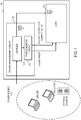
- FIG. 1 is a block diagram of an example of a wireless communication device configured to receive power from multiple types of power sources.
- the wireless communication device 100 may be a mobile phone, a smart phone, a personal digital assistant (PDA), a tablet computer, a laptop computer, a game console, a media player, a digital camera, or any other suitable device.
- PDA personal digital assistant
- the wireless device may be configured to support any suitable multiple access technology, including by way of example, Code Division Multiple Access (CDMA) systems, Multiple-Carrier CDMA (MCCDMA), Wideband CDMA (W-CDMA), High-Speed Packet Access (HSPA, HSPA+) systems, Time Division Multiple Access (TDMA) systems, Frequency Division Multiple Access (FDMA) systems, Single-Carrier FDMA (SC-FDMA) systems, Orthogonal Frequency Division Multiple Access (OFDMA) systems, or other multiple access technologies.
- CDMA Code Division Multiple Access
- MCCDMA Multiple-Carrier CDMA
- W-CDMA Wideband CDMA
- HSPA High-Speed Packet Access
- TDMA Time Division Multiple Access
- FDMA Frequency Division Multiple Access
- SC-FDMA Single-Carrier FDMA
- OFDMA Orthogonal Frequency Division Multiple Access
- the wireless communication device 100 may be further configured to support any suitable air interface standard, including by way of example, Long Term Evolution (LTE), Evolution-Data Optimized (EV-DO), Ultra Mobile Broadband (UMB), Universal Terrestrial Radio Access (UTRA), Global System for Mobile Communications (GSM), Evolved UTRA (E-UTRA), IEEE 802.11 (Wi-Fi), IEEE 802.16 (WiMAX), IEEE 802.20, Flash-OFDM, Bluetooth, or any other suitable air interface standard.
- LTE Long Term Evolution
- EV-DO Evolution-Data Optimized
- UMB Ultra Mobile Broadband
- UTRA Universal Terrestrial Radio Access
- GSM Global System for Mobile Communications
- E-UTRA Evolved UTRA
- IEEE 802.11 Wi-Fi
- IEEE 802.16 WiMAX
- IEEE 802.20 Flash-OFDM
- Bluetooth or any other suitable air interface standard.
- the actual air interface standard and the multiple access technology supported by the wireless communication device 100 will depend on the specific application and the overall design constraints imposed on
- the wireless communication device 100 includes a power management circuit 110 configured to receive power supplied from a power source 130.
- the wireless communication device 100 may be configured to receive power from different power sources.
- These power sources may include, for example, a USB charging downstream port (CDP), which may allow a current draw of up to 1000 mA.
- the power sources may further include, for example, a USB standard charging port (SCP), which may allow a current draw of up to 500 mA.
- SCP USB standard charging port
- the power sources may further include, for example, a dedicated charging port (DCP), which allows a current draw of up to 1500 mA.
- the DCP may be utilized when a USB connector is connected to a wall charger. As described, the power sources have different current supply limitations.
- the power management circuit 110 may be configured to manage power supplied from the power source 130 to a load 120.
- the power management circuit 110 includes the charger 112 (e.g., a linear charger) which receives power supplied from the power source 130 (e.g., one of the various USB ports described above) and provides a regulated or constant voltage to the load 120.
- the voltage may be provided from the power management circuit 110 via power output port 113 and received by the load 120 via power input port 114.
- the power management circuit 110 may include a power monitor circuit 111 that monitors the power supplied to the load 120.
- the power monitor circuit 111 may be configured to provide to the load 120 one or more parameters relating to the power source 130.
- the load 120 may be dynamically configurable to operate within the current capability of the power source 130 based on the one or more parameters.
- the one or more parameters may include, by way of example, a value for the instantaneous peak current drawn by the load 120. If the current capability of the power source 130 is known, the load 120 can use this parameter to configure itself such that it does not exceed the maximum current limit using various levels of current limiting schemes by making the correct tradeoffs with respect to performance, bandwidth, etc.
- the current capability of the power source 130 may be determined, in some cases, from the type of power source, which may be communicated through one of the pins on the connector between the power source 130 and the wireless communication device 100, or by other suitable means known in the art. By way of example, a USB SDP connection from a PC is known to have a maximum current of 500 mA.
- the instantaneous peak current may be measured by the power monitor circuit 111 and the measured value output from the power management circuit 110 to the load 120.
- the one or more parameters may also include, for example, a voltage indicator.
- the voltage indicator may be a status bit that is set when the power monitor circuit 111 detects that the voltage from the power source 130 is beginning to droop due to excess current draw.
- the status bit may take the form of an interrupt (VMIN INTERRUPT) that is sent from the power monitor circuit 111 to the load 120.
- the interrupt may be useful when the current capability of the power source 130 is unknown. In this case, the load 120 can read the instantaneous peak current value when it receives the interrupt and then apply various current limiting schemes to stay under the instantaneous peak current budget.
- the various instantaneous peak current value and voltage indicator discussed above are examples of parameters that may be generated by the power management circuit 110 and used by the load 120 to dynamically configure itself for operation within the current capability of the power source 130.
- other parameters may be appropriate depending on the particular application and the overall design constraints imposed on the apparatus.
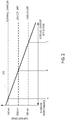
- FIG. 2 is a power diagram illustrating various current draws for an example of a wireless communication device.
- the diagram plots current draw to performance levels for the wireless communication device.
- the current limiting scheme applied by the load 120 may adjust or limit the current draw by adjusting the performance level. In this fashion, the load 120 may operate at a current consumption level meeting the current supply limit of the power source 130.
- Line 210 indicates that as the current limiting scheme increases the current mitigation level (e.g., decreasing performance level of the wireless communication device), the wireless communication device 100 may draw less current. Conversely, as the current limiting scheme decreases the current mitigation level (e.g., increasing performance level of the wireless communication device), the wireless communication device 100 may draw more current.
- the current limiting scheme may target the current mitigation level/performance level at point A to meet the current supply limit of 1500 mA.
- the current limiting scheme may target the current mitigation level/performance level at point B to meet the current supply limit of 1000 mA.
- the current limiting scheme may target the current mitigation level/performance level at point C to meet the current supply limit of 500 mA.
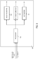
- FIG. 3 is a functional block diagram of an example of a load applying various current limiting schemes.
- the load 120 may include any number of modules and/or components.
- the load 120 may include multiple wireless transceivers, such as a 4G/3G/2.5G modem 128 to support LTE communications and a Wi-Fi modem 124 to support Wi-Fi communications.
- the 4G/3G/2.5G modem 128 may be able to perform data communication using one or more of the 4G/3G/2.5G protocols.
- the load 120 may also include an amplifier, such as an RF power amplifier 126 to support RF communications.
- the load 120 may also include other modules, components, additional amplifiers and/or circuits that are not shown.
- the load 120 may further include a processor 122.
- the processor 122 may be a single core or multiple core processor capable of managing the operations of the load 120, as well as dynamically configuring the load 120 to operate within the current capability of the power source.
- the processor 122 may be implemented with one or more general-purpose and/or special-purpose processors. Examples include microprocessors, microcontrollers, digital signal processors (DSPs), field programmable gate arrays (FPGAs), programmable logic devices (PLDs), state machines, gated logic, discrete hardware circuits, and other suitable hardware configured to perform the various functionality described throughout this disclosure.
- DSPs digital signal processors
- FPGAs field programmable gate arrays
- PLDs programmable logic devices
- state machines gated logic, discrete hardware circuits, and other suitable hardware configured to perform the various functionality described throughout this disclosure.
- One or more of the general-purpose and/or special-purpose processors may execute software.
- Software shall be construed broadly to mean instructions, instruction sets, code, code segments, program code, programs, subprograms, software modules, applications, software applications, software packages, routines, subroutines, objects, executables, threads of execution, procedures, functions, etc., whether referred to as software, firmware, middleware, microcode, hardware description language, or otherwise.
- the processor 122 may be implemented apart from the various modules or components, integrated into one of the modules or components, or distributed across any number of the modules or components.
- the processor 122 may apply the current limiting scheme, based on one or more parameters from the power management circuit 110 (see FIG. 1 ).
- the current limiting scheme may lower the performance level (e.g., increase the current mitigation) of the wireless communication device 120 and thereby reduce the current draw.
- the application of the current limiting scheme may cause the processor 122 may reduce its operations by lowering its operating frequency, lowering its operating voltage, and/or power-collapsing or hot-plugging its cores.
- Hot-plugging is an operation to power-collapse a core and to inform the operating system (OS) (e.g., hide the power-collapsed core) such that the OS does not attempt to wake up the power-collapsed core.
- OS operating system
- the processor 122 may apply the current limiting scheme to the Wi-Fi modem 124 by reducing its bandwidth and/or output power.
- the Wi-Fi modem 124 may reduce its transmission/receiving signal bandwidth, reduce transmission power, thereby reducing its operating range, and/or reduce the number of Wi-Fi clients.
- the processor 122 may apply the current limiting scheme to the RF power amplifier 126 by reducing its power, which reduces its operating range.
- the processor 122 may apply the current limiting scheme to the 4G/3G/2.5G modem 128 by reducing its bandwidth and/or changing its communication mode.
- the 4G/3G/2.5G modem 128 may lower its operation from 4G LTE, Category 4 to 4G LTE, Category 3, 2, or 1.
- the 4G/3G/2.5G modem 128 may drop from 4G LTE to 3G or 2G for wireless communication. Furthermore, the 4G/3G/2.5G modem 128 may disable certain features of LTE, such as carrier aggregation. Various other current limiting schemes may be employed in different configurations depending on the particular application and the overall design constraints imposed on the apparatus.
- FIG. 4 is a functional block diagram of an example of a power monitor circuit.
- the power monitor circuit 111 includes a current detector 410 and a voltage detector 420.
- the current detector 410 may be used to measure the instantaneous peak current provided by the power source as seen by the power monitor circuit 111. The measured instantaneous peak current may then be used to provide a value to the load 120 representing the current draw by the load 120 to support operations (see FIG. 1 ). As explained earlier, this value may be used by the load 120 to apply various current limiting schemes to ensure that the load 120 maintains operation within the current capability of the power source 130 (see FIG. 1 ).
- the voltage detector 420 may be used to monitor the voltage output from the power source 130 (see FIG. 1 ). In this configuration, the voltage detector 420 may be used to generate a voltage indicator for the load 120 (see FIG. 1 ).
- the voltage indicator may be a status bit that is set when the voltage begins to droop due to excessive current draw from the power source 130 (see FIG. 1 ). As described earlier, the status bit may take the form of an interrupt (V MIN INTERRUPT) that is sent from the power monitor circuit 111 to the load 120 (see FIG. 1 ). When the interrupt is received, the load 120 can read the instantaneous peak current value and then apply various current limiting schemes to stay under the instantaneous peak current budget (see FIG. 1 ).
- the power monitor circuit 111 may further be configured to store the instantaneous peak current value in memory 430 when the status bit is set. This allows the load 120 to continuously access the value while applying various current limiting schemes to stay under the instantaneous peak current budget (see FIG. 1 ).
- FIGS. 5A and 5B depict a flow diagram illustrating the operation of an example of a load applying a current limiting scheme.
- the operation illustrated in FIGS. 5A and 5B begins by identifying the type of power source, for example, during a boot or initializing sequence.
- the power source options are PC DSP port, PC CDP port, or wall charger.
- Other configurations may be implemented for handling other power sources, either instead of or in addition to, any of the aforementioned power sources.
- the power source may be identified through a signal on one or more pins for the connector between the power source 130 and the power management circuit 110, or by any other suitable means known in the art (see FIG. 1 ).
- a voltage or an absence of a voltage of a particular connector pin may be used by the load 120 to identify the power source 130 (see FIG. 1 ).
- step A is the current limiting scheme for a 500 mA current limit specification. If the determination is in the negative, the flow goes to 530.
- step 530 whether the power source is a CDP is determined. If the determination is in the affirmative, the flow goes to 532. At 532, whether the CDP comport to the USB 2.0 specification is determined. If the determination is in the affirmative, the flow goes to step A (the 500 mA current limiting scheme). If the determination is in the negative, the flow goes to step B, which is the current limiting scheme for a 1000 mA current limit specification. If the determination of 530 is in the negative, the flow goes to 540. At 540, whether the power source is a DCP is determined. If the determination is in the affirmative, the flow goes to step C, which is the current limiting scheme for a 1500 mA current limit specification.
- Step A 500 mA current limit specification
- the processor applies a current limiting scheme for staying under 500 mA.
- the load may select a current limiting scheme from a lookup table. Further details of the current limiting scheme lookup table are presented below in conjunction with FIG.
- the load reads the instantaneous peak current value from the power monitor circuit.
- the load may determine based on that value whether the current consumption of the wireless communication device is within the target 500 mA. If the determination is in the affirmative, the flow enters a loop at 552 to ensure the current consumption of the wireless communication device remains within budget. If the determination is negative, the flow goes back to step 550 to allow the load to apply additional current limiting scheme to reduce the current draw of the wireless communication device.
- step A 500 mA current limit specification
- the load does not need to wait for the V MIN INTERRUPT to deploy the current limiting scheme because the current capability of the power source is known.
- the 500 mA current limit provides little headroom for the wireless communication device. By not waiting for the V MIN INTERRUPT, any excess current drawn by the load may be addressed in a more timely fashion.
- Step B 1000 mA current limit specification
- the step C (1500 mA current limit specification) include steps 560, 562, 564, and 566. Although the steps B and C share in same flow in the example, that needs not be the case as would be understood by a person of ordinary skill in the art.
- the load enters a loop waiting for V MIN INTERUPT. By waiting for the V MIN INTERRUPT, the load does not need to rely on the specifications of the power sources, and therefore, can provide a more accurate current limiting scheme.
- the V MIN INTERRUPT is received, the flow goes to 562.
- the load reads the instantaneous peak current value from the power monitor circuit.
- the load applies a current limiting scheme for staying under the maximum current.
- the load may select a current limiting scheme from the current limiting scheme lookup table of FIG. 6 .
- the load may determine whether the current consumption of the wireless communication device falls within the maximum current value. If the determination is in the affirmative, the flow enters a loop at 564 to ensure the current consumption of the wireless communication device remains within budget. If the determination is in the negative, the flow goes back to step 560 to repeat the process.
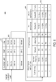
- FIG. 6 is a diagram of an example of a current limiting scheme lookup table.
- the current limiting scheme lookup table 600 stores multiple configurations of the load.
- the table 610 stores entries as a function of target current limitation, temperature, and/or leakage current information (IDDq).
- the load may select an entry 612 with a target current limit of 1500 mA, a temperature of 65 °C, and an IDDq of 145 mA.
- the selected entry 612 may refer to entries of a table 620, where the entries of the table 620 may include various configurations of the wireless communication device meeting the target current of the entry 612.
- the entries of a table 620 may include the load configurations to reduce a bandwidth, switch a communication mode, and/or reduce a range of wireless communication of the wireless communication device in order to reduce the current consumption.
- the load configurations may include processor mitigation operations, which may include the number of cores to hot-plug and a maximum operating frequency limit.
- the load configurations may further include LTE mitigation operations, which may include the network (e.g., 4G or 3G), the LTE categories, and whether carrier aggregation (CA) is enabled. These LTE mitigation operations may affect the communication mode selected (e.g., 4G or 3G; LTE categories) and the throughput or bandwidth of the LTE communications.
- the load configurations may further include RF power amplifier mitigation operations, which may include various bandwidths to reduce power. These mitigation operations may affect the range and/or bandwidth of the amplifier.
- the load configurations may further include Wi-Fi mitigation operations such as various bandwidths and the number clients.
Description
- The disclosure relates generally to electronic apparatuses, in particular, to dynamically configurable apparatus for operating within the current capabilities of the power source.
- Increasingly, current management is becoming an issue for mobile devices such as wireless communication devices. Wireless communication technologies and devices (e.g., cellular phones, wireless communication attachments for laptops, etc.) have grown in popularity and uses over the past several years. This is due, at least in part, to improvements in performance and capability that allow users to execute complex and power intensive software applications (e.g., music players, web browsers, video streaming applications, etc.). To meet the increasing performance demand, power consumptions (e.g., current draws) of these wireless communication devices have likewise increased.
- Moreover, these wireless communication devices may be configured to connect and to receive power from multiple types of power resources. For example, a wireless communication device may be connected to and received power from a laptop via one of various types of Universal Serial Bus (USB) connections. The current consumption of the wireless communication device would need to meet the restraint of the one USB type. Thus, one design challenge is to manage the current consumption of a wireless communication device for multiple types of power sources with different current supply limitations.
- Attention is drawn to
US 2013/254579 A1 , which is a system and method for managing electrical current within a portable computing device ("PCD") including assigning a priority to two or more communications supported by the PCD. A present level of power supply for the PCD may be monitored by a communications power ("CP") manager module. Next, the CP manager module may determine if the two or more communications may be transmitted at the present level of the power supply. If the two or more communications cannot be transmitted at the present level of the power supply, then the CP manager module may determine if a timing of at least one of the communications may be adjusted. The CP manager module may also determine a theoretical power level adjustment for at least one of the communications. The two or more communications may be transmitted with any calculated timing off sets and power level adjustments. - Attention is further drawn to
US 2010/216524 A1 , which discloses an apparatus providing plural wireless transceivers within a desired power budget and associated methods. A plurality of wireless communication modules, each having a lower-power state and a higher-power state, thereby controlling total power delivered by the power source to the plurality of wireless communication modules. - Attention is also drawn to
US 2013/283026 A1 , disclosing an integrated circuit device at least one compute engine and a control unit. Coupled to the compute engine(s), the control unit is adapted to dynamically control an energy efficient operating setting of at least one power management parameter for the integrated circuit device after execution of Basic Input/Output System (BIOS) has already completed. - In accordance with the present invention an apparatus, as set forth in the independent claim is provided. Preferred embodiments of the invention are described in the dependent claims.
- It is understood that other aspects of apparatus and methods will become readily apparent to those skilled in the art from the following detailed description, wherein various aspects of apparatus and methods are shown and described by way of illustration. As will be realized, these aspects may be implemented in other and different forms and its several details are capable of modification in various other respects within the scope of the appended claims.
- Accordingly, the drawings and detailed description are to be regarded as illustrative in nature and not as restrictive.
-
-
FIG. 1 is a block diagram of an example of a wireless communication device configured to receive power from multiple types of power sources. -
FIG. 2 is a power diagram illustrating various current draws for an example of a wireless communication device. -
FIG. 3 is a functional block diagram of an exemplary example of a load applying various current limiting schemes. -
FIG. 4 is a functional block diagram of an example of a power monitor circuit. -
FIGS. 5A and5B depict a flow diagram illustrating the operation of an example of a load applying a current limiting scheme. -
FIG. 6 is a diagram illustrating an example of a current limiting scheme lookup table. - The detailed description set forth below in connection with the appended drawings is intended as a description of various configurations and is not intended to represent the only configurations in which the concepts described herein may be practiced. The detailed description includes specific details for the purpose of providing a thorough understanding of various concepts. However, it will be apparent to those skilled in the art that these concepts may be practiced without these specific details. In some instances, well known structures and components are shown in block diagram form in order to avoid obscuring such concepts.
- The term "apparatus" shall be construed to include any integrated circuit or system, or any portion of an integrated circuit or system (e.g., modules, components, circuits, or the like residing in an integrated circuit or part of an integrated circuit). The term "apparatus" shall also be construed to extend to any intermediate product where an integrated circuit or system is combined with other integrated circuits or systems (e.g., a video card, a motherboard, etc.) or any end product (e.g., mobile phone, smart phone, personal digital assistant (PDA), tablet computer, laptop computer, game console, media player, digital camera, or the like). The term "method" shall similarly be construed to include the operation of any integrated circuit or system, or any portion of an integrated circuit or system, or any intermediate product or end product, or any step, process, algorithm, or the like, or any combination thereof performed by such integrated circuit or system (or portion thereof), intermediate product, or end product.
- The word "exemplary" is used herein to mean serving as an example, instance, or illustration. Any configuration described herein as "exemplary" is not necessarily to be construed as preferred or advantageous over other configurations. Likewise, the term "configuration" of an apparatus or method does not require that all configurations of the invention include the described components, structure, features, functionality, processes, advantages, benefits, or modes of operation.
- The terms "connected," "coupled," or any variant thereof, mean any connection or coupling, either direct or indirect, between two or more elements. An indirect connection encompasses the presence of one or more intermediate elements between two elements that are "connected" or "coupled" together. In contrast, when a connection or coupling is referred to as being a "direct" connection or coupling, there are no intervening elements present.
- Any reference to an element herein using a designation such as "first," "second," and so forth does not generally limit the quantity or order of those elements. Rather, these designations are used herein as a convenient method of distinguishing between two or more elements or instances of an element. Thus, a reference to first and second elements does not mean that only two elements can be employed, or that the first element must precede the second element. In addition, terminology of the form "at least one of A, B, or C" used in the description or the claims means A or B or C or any combination thereof.
- As used herein, the singular forms "a," "an" and "the" are intended to include the plural forms as well, unless the context clearly indicates otherwise. It will be further understood that the terms "comprises," "comprising," "includes" and/or "including," when used herein, specify the presence of the stated features, integers, steps, operations, elements, and/or components, but do not preclude the presence or addition of one or more other features, integers, steps, operations, elements, components, and/or groups thereof.
- Various aspects of apparatus and methods for applying current limiting schemes will be presented in the context of a wireless communication device. However, as those skilled in the art will readily appreciate, the various aspects of current limiting schemes presented throughout this disclosure are not limited thereto. Accordingly, all references to a specific application or a wireless communication device are intended only to illustrate exemplary aspects of current limiting schemes with the understanding that such aspects may have a wide range of applications.
-
FIG. 1 is a block diagram of an example of a wireless communication device configured to receive power from multiple types of power sources. Thewireless communication device 100 may be a mobile phone, a smart phone, a personal digital assistant (PDA), a tablet computer, a laptop computer, a game console, a media player, a digital camera, or any other suitable device. The wireless device may be configured to support any suitable multiple access technology, including by way of example, Code Division Multiple Access (CDMA) systems, Multiple-Carrier CDMA (MCCDMA), Wideband CDMA (W-CDMA), High-Speed Packet Access (HSPA, HSPA+) systems, Time Division Multiple Access (TDMA) systems, Frequency Division Multiple Access (FDMA) systems, Single-Carrier FDMA (SC-FDMA) systems, Orthogonal Frequency Division Multiple Access (OFDMA) systems, or other multiple access technologies. Thewireless communication device 100 may be further configured to support any suitable air interface standard, including by way of example, Long Term Evolution (LTE), Evolution-Data Optimized (EV-DO), Ultra Mobile Broadband (UMB), Universal Terrestrial Radio Access (UTRA), Global System for Mobile Communications (GSM), Evolved UTRA (E-UTRA), IEEE 802.11 (Wi-Fi), IEEE 802.16 (WiMAX), IEEE 802.20, Flash-OFDM, Bluetooth, or any other suitable air interface standard. The actual air interface standard and the multiple access technology supported by thewireless communication device 100 will depend on the specific application and the overall design constraints imposed on the system. - The
wireless communication device 100 includes apower management circuit 110 configured to receive power supplied from apower source 130. Thewireless communication device 100 may be configured to receive power from different power sources. These power sources may include, for example, a USB charging downstream port (CDP), which may allow a current draw of up to 1000 mA. The power sources may further include, for example, a USB standard charging port (SCP), which may allow a current draw of up to 500 mA. The power sources may further include, for example, a dedicated charging port (DCP), which allows a current draw of up to 1500 mA. The DCP may be utilized when a USB connector is connected to a wall charger. As described, the power sources have different current supply limitations. - The
power management circuit 110 may be configured to manage power supplied from thepower source 130 to aload 120. In the example, thepower management circuit 110 includes the charger 112 (e.g., a linear charger) which receives power supplied from the power source 130 (e.g., one of the various USB ports described above) and provides a regulated or constant voltage to theload 120. The voltage may be provided from thepower management circuit 110 viapower output port 113 and received by theload 120 viapower input port 114. - The
power management circuit 110 may include apower monitor circuit 111 that monitors the power supplied to theload 120. Thepower monitor circuit 111 may be configured to provide to theload 120 one or more parameters relating to thepower source 130. As will be explained in greater detail, theload 120 may be dynamically configurable to operate within the current capability of thepower source 130 based on the one or more parameters. - The one or more parameters may include, by way of example, a value for the instantaneous peak current drawn by the
load 120. If the current capability of thepower source 130 is known, theload 120 can use this parameter to configure itself such that it does not exceed the maximum current limit using various levels of current limiting schemes by making the correct tradeoffs with respect to performance, bandwidth, etc. The current capability of thepower source 130 may be determined, in some cases, from the type of power source, which may be communicated through one of the pins on the connector between thepower source 130 and thewireless communication device 100, or by other suitable means known in the art. By way of example, a USB SDP connection from a PC is known to have a maximum current of 500 mA. The instantaneous peak current may be measured by thepower monitor circuit 111 and the measured value output from thepower management circuit 110 to theload 120. - The one or more parameters may also include, for example, a voltage indicator. The voltage indicator may be a status bit that is set when the
power monitor circuit 111 detects that the voltage from thepower source 130 is beginning to droop due to excess current draw. The status bit may take the form of an interrupt (VMIN INTERRUPT) that is sent from thepower monitor circuit 111 to theload 120. The interrupt may be useful when the current capability of thepower source 130 is unknown. In this case, theload 120 can read the instantaneous peak current value when it receives the interrupt and then apply various current limiting schemes to stay under the instantaneous peak current budget. - The various instantaneous peak current value and voltage indicator discussed above are examples of parameters that may be generated by the
power management circuit 110 and used by theload 120 to dynamically configure itself for operation within the current capability of thepower source 130. However, as those skilled in the art will readily appreciate, other parameters may be appropriate depending on the particular application and the overall design constraints imposed on the apparatus. -
FIG. 2 is a power diagram illustrating various current draws for an example of a wireless communication device. The diagram plots current draw to performance levels for the wireless communication device. Referring toFIGS. 1 and2 , the current limiting scheme applied by theload 120 may adjust or limit the current draw by adjusting the performance level. In this fashion, theload 120 may operate at a current consumption level meeting the current supply limit of thepower source 130.Line 210 indicates that as the current limiting scheme increases the current mitigation level (e.g., decreasing performance level of the wireless communication device), thewireless communication device 100 may draw less current. Conversely, as the current limiting scheme decreases the current mitigation level (e.g., increasing performance level of the wireless communication device), thewireless communication device 100 may draw more current. For example, in the case of aDCP power source 130, the current limiting scheme may target the current mitigation level/performance level at point A to meet the current supply limit of 1500 mA. In the case of a CDP power source, the current limiting scheme may target the current mitigation level/performance level at point B to meet the current supply limit of 1000 mA. In a case of an SDP power source, the current limiting scheme may target the current mitigation level/performance level at point C to meet the current supply limit of 500 mA. -
FIG. 3 is a functional block diagram of an example of a load applying various current limiting schemes. Theload 120 may include any number of modules and/or components. By way of example, theload 120 may include multiple wireless transceivers, such as a 4G/3G/2.5G modem 128 to support LTE communications and a Wi-Fi modem 124 to support Wi-Fi communications. For example, the 4G/3G/2.5G modem 128 may be able to perform data communication using one or more of the 4G/3G/2.5G protocols. Theload 120 may also include an amplifier, such as anRF power amplifier 126 to support RF communications. Theload 120 may also include other modules, components, additional amplifiers and/or circuits that are not shown. - The
load 120 may further include aprocessor 122. Theprocessor 122 may be a single core or multiple core processor capable of managing the operations of theload 120, as well as dynamically configuring theload 120 to operate within the current capability of the power source. Theprocessor 122 may be implemented with one or more general-purpose and/or special-purpose processors. Examples include microprocessors, microcontrollers, digital signal processors (DSPs), field programmable gate arrays (FPGAs), programmable logic devices (PLDs), state machines, gated logic, discrete hardware circuits, and other suitable hardware configured to perform the various functionality described throughout this disclosure. One or more of the general-purpose and/or special-purpose processors may execute software. Software shall be construed broadly to mean instructions, instruction sets, code, code segments, program code, programs, subprograms, software modules, applications, software applications, software packages, routines, subroutines, objects, executables, threads of execution, procedures, functions, etc., whether referred to as software, firmware, middleware, microcode, hardware description language, or otherwise. Theprocessor 122 may be implemented apart from the various modules or components, integrated into one of the modules or components, or distributed across any number of the modules or components. - In the example, the
processor 122 may apply the current limiting scheme, based on one or more parameters from the power management circuit 110 (seeFIG. 1 ). The current limiting scheme may lower the performance level (e.g., increase the current mitigation) of thewireless communication device 120 and thereby reduce the current draw. For example, the application of the current limiting scheme may cause theprocessor 122 may reduce its operations by lowering its operating frequency, lowering its operating voltage, and/or power-collapsing or hot-plugging its cores. Hot-plugging is an operation to power-collapse a core and to inform the operating system (OS) (e.g., hide the power-collapsed core) such that the OS does not attempt to wake up the power-collapsed core. - The
processor 122 may apply the current limiting scheme to the Wi-Fi modem 124 by reducing its bandwidth and/or output power. For example, the Wi-Fi modem 124 may reduce its transmission/receiving signal bandwidth, reduce transmission power, thereby reducing its operating range, and/or reduce the number of Wi-Fi clients. Theprocessor 122 may apply the current limiting scheme to theRF power amplifier 126 by reducing its power, which reduces its operating range. Theprocessor 122 may apply the current limiting scheme to the 4G/3G/2.5G modem 128 by reducing its bandwidth and/or changing its communication mode. For example, the 4G/3G/2.5G modem 128 may lower its operation from 4G LTE,Category 4 to 4G LTE,Category G modem 128 may drop from 4G LTE to 3G or 2G for wireless communication. Furthermore, the 4G/3G/2.5G modem 128 may disable certain features of LTE, such as carrier aggregation. Various other current limiting schemes may be employed in different configurations depending on the particular application and the overall design constraints imposed on the apparatus. -
FIG. 4 is a functional block diagram of an example of a power monitor circuit. In this configuration, thepower monitor circuit 111 includes acurrent detector 410 and avoltage detector 420. - The
current detector 410 may be used to measure the instantaneous peak current provided by the power source as seen by thepower monitor circuit 111. The measured instantaneous peak current may then be used to provide a value to theload 120 representing the current draw by theload 120 to support operations (seeFIG. 1 ). As explained earlier, this value may be used by theload 120 to apply various current limiting schemes to ensure that theload 120 maintains operation within the current capability of the power source 130 (seeFIG. 1 ). - The
voltage detector 420 may be used to monitor the voltage output from the power source 130 (seeFIG. 1 ). In this configuration, thevoltage detector 420 may be used to generate a voltage indicator for the load 120 (seeFIG. 1 ). The voltage indicator may be a status bit that is set when the voltage begins to droop due to excessive current draw from the power source 130 (seeFIG. 1 ). As described earlier, the status bit may take the form of an interrupt (VMIN INTERRUPT) that is sent from thepower monitor circuit 111 to the load 120 (seeFIG. 1 ). When the interrupt is received, theload 120 can read the instantaneous peak current value and then apply various current limiting schemes to stay under the instantaneous peak current budget (seeFIG. 1 ). Thepower monitor circuit 111 may further be configured to store the instantaneous peak current value inmemory 430 when the status bit is set. This allows theload 120 to continuously access the value while applying various current limiting schemes to stay under the instantaneous peak current budget (seeFIG. 1 ). -
FIGS. 5A and5B depict a flow diagram illustrating the operation of an example of a load applying a current limiting scheme. The operation illustrated inFIGS. 5A and5B begins by identifying the type of power source, for example, during a boot or initializing sequence. In this configuration, the power source options are PC DSP port, PC CDP port, or wall charger. Other configurations may be implemented for handling other power sources, either instead of or in addition to, any of the aforementioned power sources. The power source may be identified through a signal on one or more pins for the connector between thepower source 130 and thepower management circuit 110, or by any other suitable means known in the art (seeFIG. 1 ). By way of example, a voltage or an absence of a voltage of a particular connector pin may be used by theload 120 to identify the power source 130 (seeFIG. 1 ). - Referring to
FIGS. 5A and5B , at 510, the boot or initialization sequence starts. At 520, whether the power source is an SDP is determined. If the determination is in the affirmative, the flow goes to step A, which is the current limiting scheme for a 500 mA current limit specification. If the determination is in the negative, the flow goes to 530. - At 530, whether the power source is a CDP is determined. If the determination is in the affirmative, the flow goes to 532. At 532, whether the CDP comport to the USB 2.0 specification is determined. If the determination is in the affirmative, the flow goes to step A (the 500 mA current limiting scheme). If the determination is in the negative, the flow goes to step B, which is the current limiting scheme for a 1000 mA current limit specification. If the determination of 530 is in the negative, the flow goes to 540. At 540, whether the power source is a DCP is determined. If the determination is in the affirmative, the flow goes to step C, which is the current limiting scheme for a 1500 mA current limit specification.
- Step A (500 mA current limit specification) includes
steps target 500 mA. If the determination is in the affirmative, the flow enters a loop at 552 to ensure the current consumption of the wireless communication device remains within budget. If the determination is negative, the flow goes back to step 550 to allow the load to apply additional current limiting scheme to reduce the current draw of the wireless communication device. - In the step A (500 mA current limit specification), the load does not need to wait for the VMIN INTERRUPT to deploy the current limiting scheme because the current capability of the power source is known. The 500 mA current limit provides little headroom for the wireless communication device. By not waiting for the VMIN INTERRUPT, any excess current drawn by the load may be addressed in a more timely fashion.
- Step B (1000 mA current limit specification) and the step C (1500 mA current limit specification) include
steps - At 562, the load reads the instantaneous peak current value from the power monitor circuit. At 564, the load applies a current limiting scheme for staying under the maximum current. In this example, the load may select a current limiting scheme from the current limiting scheme lookup table of
FIG. 6 . At 566, the load may determine whether the current consumption of the wireless communication device falls within the maximum current value. If the determination is in the affirmative, the flow enters a loop at 564 to ensure the current consumption of the wireless communication device remains within budget. If the determination is in the negative, the flow goes back to step 560 to repeat the process. -
FIG. 6 is a diagram of an example of a current limiting scheme lookup table. The current limiting scheme lookup table 600 stores multiple configurations of the load. The table 610 stores entries as a function of target current limitation, temperature, and/or leakage current information (IDDq). Thus, in one example, the load may select anentry 612 with a target current limit of 1500 mA, a temperature of 65 °C, and an IDDq of 145 mA. The selectedentry 612 may refer to entries of a table 620, where the entries of the table 620 may include various configurations of the wireless communication device meeting the target current of theentry 612. - The entries of a table 620 may include the load configurations to reduce a bandwidth, switch a communication mode, and/or reduce a range of wireless communication of the wireless communication device in order to reduce the current consumption. For example, the load configurations may include processor mitigation operations, which may include the number of cores to hot-plug and a maximum operating frequency limit. The load configurations may further include LTE mitigation operations, which may include the network (e.g., 4G or 3G), the LTE categories, and whether carrier aggregation (CA) is enabled. These LTE mitigation operations may affect the communication mode selected (e.g., 4G or 3G; LTE categories) and the throughput or bandwidth of the LTE communications. The load configurations may further include RF power amplifier mitigation operations, which may include various bandwidths to reduce power. These mitigation operations may affect the range and/or bandwidth of the amplifier. The load configurations may further include Wi-Fi mitigation operations such as various bandwidths and the number clients.
- It is understood that the specific order or hierarchy of steps in the processes disclosed is an illustration of exemplary approaches. Based upon design preferences, it is understood that the specific order or hierarchy of steps in the processes may be rearranged. Further, some steps may be combined or omitted. The accompanying method claims present elements of the various steps in a sample order, and are not meant to be limited to the specific order or hierarchy presented. The methods disclosed herein comprise one or more steps or actions for achieving the described method. The method steps and/or actions may be interchanged with one another without departing from the scope of the claims. In other words, unless a specific order of steps or actions is specified, the order and/or use of specific steps and/or actions may be modified without departing from the scope of the claims. For example, the steps may be implemented by circuits to perform the functions described herein and/or circuits generating the signals for the functions described herein, or combinations thereof.
- The previous description is provided to enable any person skilled in the art to practice the various aspects described herein. Various modifications within the scope of the appended claims to these aspects will be readily apparent to those skilled in the art, and the generic principles defined herein may be applied to other aspects. Thus, the claims are not intended to be limited to the aspects shown herein, but are to be accorded the full scope consistent with the language of the claims, wherein reference to an element in the singular is not intended to mean "one and only one" unless specifically so stated, but rather "one or more." Unless specifically stated otherwise, the term "some" refers to one or more.
Claims (13)
- An apparatus, comprising:a load (120) including a processor (122) having a plurality of cores; anda power management circuit (110) configured to manage power supplied by a power source (130) to the load (120) and provide to the load (120) one or more parameters relating to the power source (130);wherein the load (120) is dynamically configurable by the processor to operate within a current capability of the power source (130) based on the one or more parameters and to apply one or more current limiting schemes to operate within the current capability of the power source (130), the processor (122) being configured to apply the one or more current limiting schemes by hot-plugging at least one of the cores;
wherein hot-plugging is an operation to power-collapse a core. - The apparatus of claim 1, wherein the load (120) further comprises a wireless communication device.
- The apparatus of claim 1, wherein the one or more parameters comprise instantaneous peak current drawn from the power source (130).
- The apparatus of claim 3, wherein the one or more parameters comprise a voltage indicator responsive to voltage supplied by the power source (130) to the load (120).
- The apparatus of claim 1, wherein the processor (122) is further configured to apply the one or more current limiting schemes by varying at least one of operating voltage or operating frequency of the processor (122).
- The apparatus of claim 1, wherein the load (120) further comprises at least one amplifier (126) and the processor (122) is further configured to apply the one or more current limiting schemes by reducing power of the at least one amplifier (126).
- The apparatus of claim 1, wherein the load (120) further comprises a wireless transceiver (124, 128) and the processor (122) is further configured to apply the one or more current limiting schemes by changing a communication mode of the wireless transceiver (124, 128).
- The apparatus of claim 1, wherein the load (120) further comprises a wireless transceiver (124, 128) and a processor (122) configured to apply the one or more current limiting schemes by reducing bandwidth of the wireless transceiver (124, 128).
- The apparatus of claim 1, wherein the load is dynamically configurable by the processor to operate within the current capability of the power source by applying the one or more current limiting schemes.
- The apparatus of claim 9, wherein the power management circuit (110) is further configured to provide to the load (120) one or more parameters relating to the power source (130), and wherein the load (120) is configured to applying the one or more current limiting schemes based on the one or more parameters.
- The apparatus of claim 9, wherein the one or more parameters comprise instantaneous peak current drawn from the power source (130).
- The apparatus of claim 9, wherein the one or more parameters comprise a voltage indicator responsive to voltage supplied by the power source (130) to the load (120).
- The apparatus of claim 1, wherein the load (120) is dynamically configurable by the processor to limit the current drawn from the power source (130) based on the current capability of the power source (130).
Applications Claiming Priority (2)
| Application Number | Priority Date | Filing Date | Title |
|---|---|---|---|
| US14/836,793 US10117196B2 (en) | 2015-08-26 | 2015-08-26 | Dynamically configurable apparatus for operating within the current capabilities of the power source |
| PCT/US2016/041780 WO2017034688A1 (en) | 2015-08-26 | 2016-07-11 | Dynamically configurable apparatus for operating within the current capabilities of the power source |
Publications (2)
| Publication Number | Publication Date |
|---|---|
| EP3342047A1 EP3342047A1 (en) | 2018-07-04 |
| EP3342047B1 true EP3342047B1 (en) | 2021-05-19 |
Family
ID=56511939
Family Applications (1)
| Application Number | Title | Priority Date | Filing Date |
|---|---|---|---|
| EP16742135.3A Active EP3342047B1 (en) | 2015-08-26 | 2016-07-11 | Dynamically configurable apparatus for operating within the current capabilities of the power source |
Country Status (9)
| Country | Link |
|---|---|
| US (1) | US10117196B2 (en) |
| EP (1) | EP3342047B1 (en) |
| JP (1) | JP6505946B2 (en) |
| KR (1) | KR101962459B1 (en) |
| CN (1) | CN107925425B (en) |
| BR (1) | BR112018003547A2 (en) |
| JO (1) | JO3642B1 (en) |
| TW (1) | TWI685269B (en) |
| WO (1) | WO2017034688A1 (en) |
Families Citing this family (3)
| Publication number | Priority date | Publication date | Assignee | Title |
|---|---|---|---|---|
| US10440645B2 (en) * | 2016-10-11 | 2019-10-08 | Verizon Patent And Licensing Inc. | Extending signal coverage and charge duration of a user equipment |
| KR102419492B1 (en) * | 2017-03-28 | 2022-07-11 | 삼성전자주식회사 | Electronic device and transmission power controlling method |
| US11934841B2 (en) * | 2021-07-27 | 2024-03-19 | Dell Products L.P. | System and method for managing a power supply management namespace during a chassis boot up |
Citations (1)
| Publication number | Priority date | Publication date | Assignee | Title |
|---|---|---|---|---|
| US20050064829A1 (en) * | 2003-09-19 | 2005-03-24 | Inyup Kang | Power collapse for a wireless terminal |
Family Cites Families (21)
| Publication number | Priority date | Publication date | Assignee | Title |
|---|---|---|---|---|
| US7197656B2 (en) | 2002-05-24 | 2007-03-27 | Intel Corporation | Providing overload protection in battery operation |
| US8588727B2 (en) * | 2008-03-21 | 2013-11-19 | Qualcomm Incorporated | Adaptive linearity communication device |
| US9105323B2 (en) * | 2009-01-23 | 2015-08-11 | Micron Technology, Inc. | Memory device power managers and methods |
| WO2010094119A1 (en) | 2009-02-23 | 2010-08-26 | Sierra Wireless, Inc. | Apparatus providing plural wireless transceivers within a desired power budget and associated method |
| US8892931B2 (en) * | 2009-10-20 | 2014-11-18 | Empire Technology Development Llc | Power channel monitor for a multicore processor |
| US8069356B2 (en) | 2010-01-06 | 2011-11-29 | Apple Inc. | Accessory power management |
| US8510582B2 (en) | 2010-07-21 | 2013-08-13 | Advanced Micro Devices, Inc. | Managing current and power in a computing system |
| US9026823B2 (en) * | 2010-08-26 | 2015-05-05 | Renesas Electronics Corporation | Data processing device and data processing system with wide voltage range operation mode |
| KR101770587B1 (en) * | 2011-02-21 | 2017-08-24 | 삼성전자주식회사 | A method of hot plugging of multi-core processor and multi-core processor system |
| US8548475B2 (en) * | 2011-08-17 | 2013-10-01 | Apple Inc. | Method for optimizing power consumption in wireless devices using data rate efficiency factor |
| JP2013078163A (en) * | 2011-09-29 | 2013-04-25 | Renesas Electronics Corp | Semiconductor device and electronic circuit device |
| WO2013060802A1 (en) | 2011-10-25 | 2013-05-02 | St-Ericsson Sa | Battery-operated electronic device and method |
| JP5773920B2 (en) * | 2012-03-19 | 2015-09-02 | ルネサスエレクトロニクス株式会社 | Charger |
| US9223376B2 (en) | 2012-03-23 | 2015-12-29 | Qualcomm Incorporated | Managing electrical current in a portable computing device when two or more communications overlap in drawing power during a transmission |
| US9360909B2 (en) | 2012-04-19 | 2016-06-07 | Intel Corporation | System, method and apparatus for energy efficiency and energy conservation by configuring power management parameters during run time |
| TWI461891B (en) * | 2012-10-19 | 2014-11-21 | Wistron Corp | Power managing circuit and the method thereof |
| KR20140068737A (en) * | 2012-11-28 | 2014-06-09 | 삼성전자주식회사 | Apparatus and method for controlling current consumption of mobile terminal |
| US9268393B2 (en) * | 2012-11-30 | 2016-02-23 | Intel Corporation | Enforcing a power consumption duty cycle in a processor |
| US9798367B2 (en) | 2013-04-09 | 2017-10-24 | Intel Corporation | Controlling supply of power to computing devices with dynamically variable energy capacity |
| KR102200711B1 (en) * | 2013-10-11 | 2021-01-12 | 삼성전자주식회사 | Method and apparatus for controlling power considering energy efficiency in the mimo communication system |
| JP6140897B2 (en) * | 2013-11-29 | 2017-06-07 | メディアテック インコーポレイテッド | Method and controller for reducing power for systems on portable devices, corresponding portable devices, and corresponding computer program products |
-
2015
- 2015-08-26 US US14/836,793 patent/US10117196B2/en active Active
-
2016
- 2016-07-11 WO PCT/US2016/041780 patent/WO2017034688A1/en active Application Filing
- 2016-07-11 EP EP16742135.3A patent/EP3342047B1/en active Active
- 2016-07-11 KR KR1020187005476A patent/KR101962459B1/en active IP Right Grant
- 2016-07-11 CN CN201680048670.8A patent/CN107925425B/en not_active Expired - Fee Related
- 2016-07-11 JP JP2018510335A patent/JP6505946B2/en active Active
- 2016-07-11 BR BR112018003547A patent/BR112018003547A2/en not_active IP Right Cessation
- 2016-08-07 JO JOP/2016/0175A patent/JO3642B1/en active
- 2016-08-15 TW TW105125968A patent/TWI685269B/en not_active IP Right Cessation
Patent Citations (1)
| Publication number | Priority date | Publication date | Assignee | Title |
|---|---|---|---|---|
| US20050064829A1 (en) * | 2003-09-19 | 2005-03-24 | Inyup Kang | Power collapse for a wireless terminal |
Also Published As
| Publication number | Publication date |
|---|---|
| CN107925425A (en) | 2018-04-17 |
| TW201722186A (en) | 2017-06-16 |
| EP3342047A1 (en) | 2018-07-04 |
| JO3642B1 (en) | 2020-08-27 |
| KR101962459B1 (en) | 2019-03-26 |
| CN107925425B (en) | 2020-09-01 |
| KR20180044293A (en) | 2018-05-02 |
| JP6505946B2 (en) | 2019-04-24 |
| US10117196B2 (en) | 2018-10-30 |
| TWI685269B (en) | 2020-02-11 |
| US20170064650A1 (en) | 2017-03-02 |
| BR112018003547A2 (en) | 2018-09-25 |
| WO2017034688A1 (en) | 2017-03-02 |
| JP2018532297A (en) | 2018-11-01 |
Similar Documents
| Publication | Publication Date | Title |
|---|---|---|
| US9942851B2 (en) | Dynamic power management in a wireless device | |
| US11068041B2 (en) | Method to enhance device policy management (DPM) power sharing for USB Type-C (USB-C) only devices | |
| US10491003B2 (en) | Multiple input single inductor multiple output regulator | |
| KR101832953B1 (en) | Remote wakeup of application processor of mobile device | |
| US9804857B2 (en) | Method and apparatus for multi-mode mobile computing devices and peripherals | |
| KR101840287B1 (en) | Mobile device | |
| EP2882067B1 (en) | Battery-charging apparatus and method of electronic device | |
| US9055543B2 (en) | Reduced power wireless wake on connection | |
| EP3342047B1 (en) | Dynamically configurable apparatus for operating within the current capabilities of the power source | |
| US20150121095A1 (en) | Hub device for universal serial bus and power management method thereof | |
| US20190086994A1 (en) | Transition of an input / output port in a suspend mode from a high-current mode | |
| JP2018517955A (en) | Clock generation circuit with standby mode for fast startup | |
| US20180335830A1 (en) | Power management system | |
| EP4184287A1 (en) | Role detection for usb-based charging | |
| WO2010067400A1 (en) | Power use method, slave device, and computer program | |
| TW201541803A (en) | Portable electronic apparatus and charging control method thereof | |
| EP4227768A1 (en) | Role detection for usb-based charging | |
| CN110633001A (en) | Electronic equipment control method and device and electronic equipment | |
| TWI469053B (en) | Electronic device and startup method therefore | |
| US20230385218A1 (en) | Usb type-c subsystem | |
| US10401931B2 (en) | Power delivery architecture to increase performance of computing systems when docked | |
| US11705750B2 (en) | Power negotiation sequence to improve user experience and battery life | |
| US20230409100A1 (en) | Dynamic input power monitor | |
| CN116707055A (en) | Charging circuit, electronic device and reverse charging method |
Legal Events
| Date | Code | Title | Description |
|---|---|---|---|
| STAA | Information on the status of an ep patent application or granted ep patent |
Free format text: STATUS: THE INTERNATIONAL PUBLICATION HAS BEEN MADE |
|
| PUAI | Public reference made under article 153(3) epc to a published international application that has entered the european phase |
Free format text: ORIGINAL CODE: 0009012 |
|
| STAA | Information on the status of an ep patent application or granted ep patent |
Free format text: STATUS: REQUEST FOR EXAMINATION WAS MADE |
|
| 17P | Request for examination filed |
Effective date: 20180112 |
|
| AK | Designated contracting states |
Kind code of ref document: A1 Designated state(s): AL AT BE BG CH CY CZ DE DK EE ES FI FR GB GR HR HU IE IS IT LI LT LU LV MC MK MT NL NO PL PT RO RS SE SI SK SM TR |
|
| AX | Request for extension of the european patent |
Extension state: BA ME |
|
| DAV | Request for validation of the european patent (deleted) | ||
| DAX | Request for extension of the european patent (deleted) | ||
| RIC1 | Information provided on ipc code assigned before grant |
Ipc: H04W 52/02 20090101ALI20170315BHEP Ipc: H04W 76/04 20090101ALI20170315BHEP Ipc: H04B 1/18 20060101AFI20170315BHEP |
|
| STAA | Information on the status of an ep patent application or granted ep patent |
Free format text: STATUS: EXAMINATION IS IN PROGRESS |
|
| 17Q | First examination report despatched |
Effective date: 20190909 |
|
| REG | Reference to a national code |
Ref country code: DE Ref legal event code: R079 Ref document number: 602016058050 Country of ref document: DE Free format text: PREVIOUS MAIN CLASS: H04B0001180000 Ipc: H04W0052020000 |
|
| GRAP | Despatch of communication of intention to grant a patent |
Free format text: ORIGINAL CODE: EPIDOSNIGR1 |
|
| STAA | Information on the status of an ep patent application or granted ep patent |
Free format text: STATUS: GRANT OF PATENT IS INTENDED |
|
| RIC1 | Information provided on ipc code assigned before grant |
Ipc: H04B 1/18 20060101ALI20201123BHEP Ipc: H04W 52/02 20090101AFI20201123BHEP |
|
| INTG | Intention to grant announced |
Effective date: 20201208 |
|
| GRAS | Grant fee paid |
Free format text: ORIGINAL CODE: EPIDOSNIGR3 |
|
| GRAA | (expected) grant |
Free format text: ORIGINAL CODE: 0009210 |
|
| STAA | Information on the status of an ep patent application or granted ep patent |
Free format text: STATUS: THE PATENT HAS BEEN GRANTED |
|
| AK | Designated contracting states |
Kind code of ref document: B1 Designated state(s): AL AT BE BG CH CY CZ DE DK EE ES FI FR GB GR HR HU IE IS IT LI LT LU LV MC MK MT NL NO PL PT RO RS SE SI SK SM TR |
|
| REG | Reference to a national code |
Ref country code: GB Ref legal event code: FG4D |
|
| REG | Reference to a national code |
Ref country code: CH Ref legal event code: EP |
|
| REG | Reference to a national code |
Ref country code: DE Ref legal event code: R096 Ref document number: 602016058050 Country of ref document: DE |
|
| REG | Reference to a national code |
Ref country code: AT Ref legal event code: REF Ref document number: 1395219 Country of ref document: AT Kind code of ref document: T Effective date: 20210615 |
|
| REG | Reference to a national code |
Ref country code: IE Ref legal event code: FG4D |
|
| REG | Reference to a national code |
Ref country code: LT Ref legal event code: MG9D |
|
| REG | Reference to a national code |
Ref country code: AT Ref legal event code: MK05 Ref document number: 1395219 Country of ref document: AT Kind code of ref document: T Effective date: 20210519 |
|
| REG | Reference to a national code |
Ref country code: NL Ref legal event code: MP Effective date: 20210519 |
|
| PG25 | Lapsed in a contracting state [announced via postgrant information from national office to epo] |
Ref country code: HR Free format text: LAPSE BECAUSE OF FAILURE TO SUBMIT A TRANSLATION OF THE DESCRIPTION OR TO PAY THE FEE WITHIN THE PRESCRIBED TIME-LIMIT Effective date: 20210519 Ref country code: AT Free format text: LAPSE BECAUSE OF FAILURE TO SUBMIT A TRANSLATION OF THE DESCRIPTION OR TO PAY THE FEE WITHIN THE PRESCRIBED TIME-LIMIT Effective date: 20210519 Ref country code: BG Free format text: LAPSE BECAUSE OF FAILURE TO SUBMIT A TRANSLATION OF THE DESCRIPTION OR TO PAY THE FEE WITHIN THE PRESCRIBED TIME-LIMIT Effective date: 20210819 Ref country code: LT Free format text: LAPSE BECAUSE OF FAILURE TO SUBMIT A TRANSLATION OF THE DESCRIPTION OR TO PAY THE FEE WITHIN THE PRESCRIBED TIME-LIMIT Effective date: 20210519 Ref country code: FI Free format text: LAPSE BECAUSE OF FAILURE TO SUBMIT A TRANSLATION OF THE DESCRIPTION OR TO PAY THE FEE WITHIN THE PRESCRIBED TIME-LIMIT Effective date: 20210519 |
|
| PG25 | Lapsed in a contracting state [announced via postgrant information from national office to epo] |
Ref country code: RS Free format text: LAPSE BECAUSE OF FAILURE TO SUBMIT A TRANSLATION OF THE DESCRIPTION OR TO PAY THE FEE WITHIN THE PRESCRIBED TIME-LIMIT Effective date: 20210519 Ref country code: SE Free format text: LAPSE BECAUSE OF FAILURE TO SUBMIT A TRANSLATION OF THE DESCRIPTION OR TO PAY THE FEE WITHIN THE PRESCRIBED TIME-LIMIT Effective date: 20210519 Ref country code: PL Free format text: LAPSE BECAUSE OF FAILURE TO SUBMIT A TRANSLATION OF THE DESCRIPTION OR TO PAY THE FEE WITHIN THE PRESCRIBED TIME-LIMIT Effective date: 20210519 Ref country code: NO Free format text: LAPSE BECAUSE OF FAILURE TO SUBMIT A TRANSLATION OF THE DESCRIPTION OR TO PAY THE FEE WITHIN THE PRESCRIBED TIME-LIMIT Effective date: 20210819 Ref country code: PT Free format text: LAPSE BECAUSE OF FAILURE TO SUBMIT A TRANSLATION OF THE DESCRIPTION OR TO PAY THE FEE WITHIN THE PRESCRIBED TIME-LIMIT Effective date: 20210920 Ref country code: GR Free format text: LAPSE BECAUSE OF FAILURE TO SUBMIT A TRANSLATION OF THE DESCRIPTION OR TO PAY THE FEE WITHIN THE PRESCRIBED TIME-LIMIT Effective date: 20210820 Ref country code: LV Free format text: LAPSE BECAUSE OF FAILURE TO SUBMIT A TRANSLATION OF THE DESCRIPTION OR TO PAY THE FEE WITHIN THE PRESCRIBED TIME-LIMIT Effective date: 20210519 Ref country code: IS Free format text: LAPSE BECAUSE OF FAILURE TO SUBMIT A TRANSLATION OF THE DESCRIPTION OR TO PAY THE FEE WITHIN THE PRESCRIBED TIME-LIMIT Effective date: 20210919 |
|
| PG25 | Lapsed in a contracting state [announced via postgrant information from national office to epo] |
Ref country code: NL Free format text: LAPSE BECAUSE OF FAILURE TO SUBMIT A TRANSLATION OF THE DESCRIPTION OR TO PAY THE FEE WITHIN THE PRESCRIBED TIME-LIMIT Effective date: 20210519 |
|
| PG25 | Lapsed in a contracting state [announced via postgrant information from national office to epo] |
Ref country code: DK Free format text: LAPSE BECAUSE OF FAILURE TO SUBMIT A TRANSLATION OF THE DESCRIPTION OR TO PAY THE FEE WITHIN THE PRESCRIBED TIME-LIMIT Effective date: 20210519 Ref country code: CZ Free format text: LAPSE BECAUSE OF FAILURE TO SUBMIT A TRANSLATION OF THE DESCRIPTION OR TO PAY THE FEE WITHIN THE PRESCRIBED TIME-LIMIT Effective date: 20210519 Ref country code: EE Free format text: LAPSE BECAUSE OF FAILURE TO SUBMIT A TRANSLATION OF THE DESCRIPTION OR TO PAY THE FEE WITHIN THE PRESCRIBED TIME-LIMIT Effective date: 20210519 Ref country code: SM Free format text: LAPSE BECAUSE OF FAILURE TO SUBMIT A TRANSLATION OF THE DESCRIPTION OR TO PAY THE FEE WITHIN THE PRESCRIBED TIME-LIMIT Effective date: 20210519 Ref country code: SK Free format text: LAPSE BECAUSE OF FAILURE TO SUBMIT A TRANSLATION OF THE DESCRIPTION OR TO PAY THE FEE WITHIN THE PRESCRIBED TIME-LIMIT Effective date: 20210519 Ref country code: RO Free format text: LAPSE BECAUSE OF FAILURE TO SUBMIT A TRANSLATION OF THE DESCRIPTION OR TO PAY THE FEE WITHIN THE PRESCRIBED TIME-LIMIT Effective date: 20210519 Ref country code: ES Free format text: LAPSE BECAUSE OF FAILURE TO SUBMIT A TRANSLATION OF THE DESCRIPTION OR TO PAY THE FEE WITHIN THE PRESCRIBED TIME-LIMIT Effective date: 20210519 |
|
| REG | Reference to a national code |
Ref country code: DE Ref legal event code: R097 Ref document number: 602016058050 Country of ref document: DE |
|
| REG | Reference to a national code |
Ref country code: CH Ref legal event code: PL |
|
| PLBE | No opposition filed within time limit |
Free format text: ORIGINAL CODE: 0009261 |
|
| STAA | Information on the status of an ep patent application or granted ep patent |
Free format text: STATUS: NO OPPOSITION FILED WITHIN TIME LIMIT |
|
| PG25 | Lapsed in a contracting state [announced via postgrant information from national office to epo] |
Ref country code: MC Free format text: LAPSE BECAUSE OF FAILURE TO SUBMIT A TRANSLATION OF THE DESCRIPTION OR TO PAY THE FEE WITHIN THE PRESCRIBED TIME-LIMIT Effective date: 20210519 |
|
| REG | Reference to a national code |
Ref country code: BE Ref legal event code: MM Effective date: 20210731 |
|
| 26N | No opposition filed |
Effective date: 20220222 |
|
| PG25 | Lapsed in a contracting state [announced via postgrant information from national office to epo] |
Ref country code: LI Free format text: LAPSE BECAUSE OF NON-PAYMENT OF DUE FEES Effective date: 20210731 Ref country code: CH Free format text: LAPSE BECAUSE OF NON-PAYMENT OF DUE FEES Effective date: 20210731 |
|
| PG25 | Lapsed in a contracting state [announced via postgrant information from national office to epo] |
Ref country code: IS Free format text: LAPSE BECAUSE OF FAILURE TO SUBMIT A TRANSLATION OF THE DESCRIPTION OR TO PAY THE FEE WITHIN THE PRESCRIBED TIME-LIMIT Effective date: 20210919 Ref country code: LU Free format text: LAPSE BECAUSE OF NON-PAYMENT OF DUE FEES Effective date: 20210711 Ref country code: AL Free format text: LAPSE BECAUSE OF FAILURE TO SUBMIT A TRANSLATION OF THE DESCRIPTION OR TO PAY THE FEE WITHIN THE PRESCRIBED TIME-LIMIT Effective date: 20210519 |
|
| PG25 | Lapsed in a contracting state [announced via postgrant information from national office to epo] |
Ref country code: IT Free format text: LAPSE BECAUSE OF FAILURE TO SUBMIT A TRANSLATION OF THE DESCRIPTION OR TO PAY THE FEE WITHIN THE PRESCRIBED TIME-LIMIT Effective date: 20210519 Ref country code: IE Free format text: LAPSE BECAUSE OF NON-PAYMENT OF DUE FEES Effective date: 20210711 Ref country code: BE Free format text: LAPSE BECAUSE OF NON-PAYMENT OF DUE FEES Effective date: 20210731 |
|
| PG25 | Lapsed in a contracting state [announced via postgrant information from national office to epo] |
Ref country code: HU Free format text: LAPSE BECAUSE OF FAILURE TO SUBMIT A TRANSLATION OF THE DESCRIPTION OR TO PAY THE FEE WITHIN THE PRESCRIBED TIME-LIMIT; INVALID AB INITIO Effective date: 20160711 |
|
| PG25 | Lapsed in a contracting state [announced via postgrant information from national office to epo] |
Ref country code: CY Free format text: LAPSE BECAUSE OF FAILURE TO SUBMIT A TRANSLATION OF THE DESCRIPTION OR TO PAY THE FEE WITHIN THE PRESCRIBED TIME-LIMIT Effective date: 20210519 |
|
| PGFP | Annual fee paid to national office [announced via postgrant information from national office to epo] |
Ref country code: FR Payment date: 20230616 Year of fee payment: 8 |
|
| PGFP | Annual fee paid to national office [announced via postgrant information from national office to epo] |
Ref country code: GB Payment date: 20230614 Year of fee payment: 8 |
|
| PGFP | Annual fee paid to national office [announced via postgrant information from national office to epo] |
Ref country code: DE Payment date: 20230614 Year of fee payment: 8 |