EP3338051B1 - Distributed delay-line for low-coherence interferometry - Google Patents
Distributed delay-line for low-coherence interferometry Download PDFInfo
- Publication number
- EP3338051B1 EP3338051B1 EP16757209.8A EP16757209A EP3338051B1 EP 3338051 B1 EP3338051 B1 EP 3338051B1 EP 16757209 A EP16757209 A EP 16757209A EP 3338051 B1 EP3338051 B1 EP 3338051B1
- Authority
- EP
- European Patent Office
- Prior art keywords
- group delay
- coherence tomography
- tomography system
- optical coherence
- optical
- Prior art date
- Legal status (The legal status is an assumption and is not a legal conclusion. Google has not performed a legal analysis and makes no representation as to the accuracy of the status listed.)
- Active
Links
Images

Classifications
-
- G—PHYSICS
- G01—MEASURING; TESTING
- G01B—MEASURING LENGTH, THICKNESS OR SIMILAR LINEAR DIMENSIONS; MEASURING ANGLES; MEASURING AREAS; MEASURING IRREGULARITIES OF SURFACES OR CONTOURS
- G01B9/00—Measuring instruments characterised by the use of optical techniques
- G01B9/02—Interferometers
- G01B9/0209—Low-coherence interferometers
- G01B9/02091—Tomographic interferometers, e.g. based on optical coherence
-
- G—PHYSICS
- G01—MEASURING; TESTING
- G01B—MEASURING LENGTH, THICKNESS OR SIMILAR LINEAR DIMENSIONS; MEASURING ANGLES; MEASURING AREAS; MEASURING IRREGULARITIES OF SURFACES OR CONTOURS
- G01B9/00—Measuring instruments characterised by the use of optical techniques
- G01B9/02—Interferometers
- G01B9/02015—Interferometers characterised by the beam path configuration
- G01B9/02027—Two or more interferometric channels or interferometers
- G01B9/02028—Two or more reference or object arms in one interferometer
-
- G—PHYSICS
- G01—MEASURING; TESTING
- G01B—MEASURING LENGTH, THICKNESS OR SIMILAR LINEAR DIMENSIONS; MEASURING ANGLES; MEASURING AREAS; MEASURING IRREGULARITIES OF SURFACES OR CONTOURS
- G01B9/00—Measuring instruments characterised by the use of optical techniques
- G01B9/02—Interferometers
- G01B9/02049—Interferometers characterised by particular mechanical design details
- G01B9/02051—Integrated design, e.g. on-chip or monolithic
-
- G—PHYSICS
- G02—OPTICS
- G02B—OPTICAL ELEMENTS, SYSTEMS OR APPARATUS
- G02B6/00—Light guides; Structural details of arrangements comprising light guides and other optical elements, e.g. couplings
- G02B6/10—Light guides; Structural details of arrangements comprising light guides and other optical elements, e.g. couplings of the optical waveguide type
- G02B6/12—Light guides; Structural details of arrangements comprising light guides and other optical elements, e.g. couplings of the optical waveguide type of the integrated circuit kind
- G02B6/12004—Combinations of two or more optical elements
-
- G—PHYSICS
- G02—OPTICS
- G02B—OPTICAL ELEMENTS, SYSTEMS OR APPARATUS
- G02B6/00—Light guides; Structural details of arrangements comprising light guides and other optical elements, e.g. couplings
- G02B6/10—Light guides; Structural details of arrangements comprising light guides and other optical elements, e.g. couplings of the optical waveguide type
- G02B6/12—Light guides; Structural details of arrangements comprising light guides and other optical elements, e.g. couplings of the optical waveguide type of the integrated circuit kind
- G02B6/12007—Light guides; Structural details of arrangements comprising light guides and other optical elements, e.g. couplings of the optical waveguide type of the integrated circuit kind forming wavelength selective elements, e.g. multiplexer, demultiplexer
-
- G—PHYSICS
- G02—OPTICS
- G02B—OPTICAL ELEMENTS, SYSTEMS OR APPARATUS
- G02B6/00—Light guides; Structural details of arrangements comprising light guides and other optical elements, e.g. couplings
- G02B6/24—Coupling light guides
- G02B6/26—Optical coupling means
- G02B6/28—Optical coupling means having data bus means, i.e. plural waveguides interconnected and providing an inherently bidirectional system by mixing and splitting signals
- G02B6/2804—Optical coupling means having data bus means, i.e. plural waveguides interconnected and providing an inherently bidirectional system by mixing and splitting signals forming multipart couplers without wavelength selective elements, e.g. "T" couplers, star couplers
- G02B6/2861—Optical coupling means having data bus means, i.e. plural waveguides interconnected and providing an inherently bidirectional system by mixing and splitting signals forming multipart couplers without wavelength selective elements, e.g. "T" couplers, star couplers using fibre optic delay lines and optical elements associated with them, e.g. for use in signal processing, e.g. filtering
-
- G—PHYSICS
- G02—OPTICS
- G02B—OPTICAL ELEMENTS, SYSTEMS OR APPARATUS
- G02B6/00—Light guides; Structural details of arrangements comprising light guides and other optical elements, e.g. couplings
- G02B6/24—Coupling light guides
- G02B6/26—Optical coupling means
- G02B6/28—Optical coupling means having data bus means, i.e. plural waveguides interconnected and providing an inherently bidirectional system by mixing and splitting signals
- G02B6/293—Optical coupling means having data bus means, i.e. plural waveguides interconnected and providing an inherently bidirectional system by mixing and splitting signals with wavelength selective means
- G02B6/29346—Optical coupling means having data bus means, i.e. plural waveguides interconnected and providing an inherently bidirectional system by mixing and splitting signals with wavelength selective means operating by wave or beam interference
- G02B6/2935—Mach-Zehnder configuration, i.e. comprising separate splitting and combining means
-
- G—PHYSICS
- G02—OPTICS
- G02B—OPTICAL ELEMENTS, SYSTEMS OR APPARATUS
- G02B6/00—Light guides; Structural details of arrangements comprising light guides and other optical elements, e.g. couplings
- G02B6/24—Coupling light guides
- G02B6/42—Coupling light guides with opto-electronic elements
- G02B6/43—Arrangements comprising a plurality of opto-electronic elements and associated optical interconnections
-
- A—HUMAN NECESSITIES
- A61—MEDICAL OR VETERINARY SCIENCE; HYGIENE
- A61B—DIAGNOSIS; SURGERY; IDENTIFICATION
- A61B3/00—Apparatus for testing the eyes; Instruments for examining the eyes
- A61B3/10—Objective types, i.e. instruments for examining the eyes independent of the patients' perceptions or reactions
- A61B3/102—Objective types, i.e. instruments for examining the eyes independent of the patients' perceptions or reactions for optical coherence tomography [OCT]
-
- G—PHYSICS
- G01—MEASURING; TESTING
- G01B—MEASURING LENGTH, THICKNESS OR SIMILAR LINEAR DIMENSIONS; MEASURING ANGLES; MEASURING AREAS; MEASURING IRREGULARITIES OF SURFACES OR CONTOURS
- G01B2290/00—Aspects of interferometers not specifically covered by any group under G01B9/02
- G01B2290/35—Mechanical variable delay line
-
- G—PHYSICS
- G01—MEASURING; TESTING
- G01B—MEASURING LENGTH, THICKNESS OR SIMILAR LINEAR DIMENSIONS; MEASURING ANGLES; MEASURING AREAS; MEASURING IRREGULARITIES OF SURFACES OR CONTOURS
- G01B2290/00—Aspects of interferometers not specifically covered by any group under G01B9/02
- G01B2290/40—Non-mechanical variable delay line
-
- G—PHYSICS
- G02—OPTICS
- G02B—OPTICAL ELEMENTS, SYSTEMS OR APPARATUS
- G02B6/00—Light guides; Structural details of arrangements comprising light guides and other optical elements, e.g. couplings
- G02B6/10—Light guides; Structural details of arrangements comprising light guides and other optical elements, e.g. couplings of the optical waveguide type
- G02B6/12—Light guides; Structural details of arrangements comprising light guides and other optical elements, e.g. couplings of the optical waveguide type of the integrated circuit kind
- G02B2006/12133—Functions
- G02B2006/12142—Modulator
Definitions
- Embodiments of the invention relate to designs of, and methods of using, distributed delay-line for use in an optical coherence tomography system.
- OCT Optical Coherence Tomography
- Time Domain Optical Coherence Tomography utilizes a variable path length in the interferometric detection system that changes in time.
- one of the elements in a TD-OCT system may be a variable delay line, which may be used to perform the depth scan (or axial scan) inside the sample.
- WIPO Patent Application Publication No. 2013/001032 A1 describes a proposed multiplexing scheme that spreads the light into paths with different lengths using a modulator in at least one of the paths so as to separate them in frequency channels. In this way, the axial scanning distance is increased, avoiding the subsequent scanning increase in the variable delay component.
- US 6,775,007 B2 discloses an OCT system, comprising an illumination source, reference and sample arms, and a detector, and characterized in that the reference arms substantially simultaneously create a plurality of reference delays for scanning a sample at respective depths, and wherein the depth information is encoded into frequency.
- US 2014/078510 A1 discloses a scanning device for low coherence interferometry.
- the low coherence interferometry system includes a first multiplexing unit and a second multiplexing unit, wherein the first multiplexing unit is configured to receive a first beam of radiation and includes a first plurality of optical delay elements configured to introduce a group delay to the first beam of radiation based on an optical path traversed by the first beam of radiation among a first plurality of optical wave guides and wherein the second multiplexing unit is configured to receive a second beam of radiation.
- the bandwidth of the system may restrict the OCT performance in terms of scanning speed.
- Both phase and amplitude modulation at frequencies close to the bandwidth edges elicit nonlinear behavior.
- phase modulation at higher frequencies generates a non-uniform optical phase response along the temperature variation. As a result, the frequency response will experience a broadening.
- the present invention relates to optical coherence tomography systems with the features of independent claim 1 and independent claim 10. Possible embodiments of the invention are subject-matter of the dependent claims.
- a modulation scheme based on a variable delay line is proposed by means of frequency multiplexing. Such multiplexing is performed by keeping one modulating frequency, but having different scanning ranges and speeds per channel.
- the TD-OCT system presented here uses a modulation scheme that multiplexes the scanning range of the delay line into different spectral bands.
- a modulation scheme may allow for power consumption reduction compared with a single delay line element since the same modulation pattern is being used for several channels.
- references in the specification to "one embodiment,” “an embodiment,” “an example embodiment,” etc. indicate that the embodiment described may include a particular feature, structure, or characteristic, but every embodiment may not necessarily include the particular feature, structure, or characteristic. Moreover, such phrases do not necessarily refer to the same embodiment. Further, when a particular feature, structure or characteristic is described in connection with an embodiment, it would be within the knowledge of one skilled in the art to effect such feature, structure or characteristic in connection with other embodiments whether or not explicitly described.
- Embodiments described herein provide systems and methods for introducing a group delay to a beam of radiation within an interferometric device.
- the interferometric device may use low coherence interferometry such as optical coherence tomography (OCT) to provide image data at different depths within a sample. Varying the group delay of the light corresponds to varying a scan depth within the sample under study.
- OCT optical coherence tomography
- the embodiments described herein are primarily directed to a modulation scheme for axial scanning, these embodiments may be combined with known lateral scanning systems to generate 3D volumetric images.
- the group delay is varied by controlling the index of refraction of a waveguide material that is guiding the beam of radiation. This may be achieved, for example, by having a waveguide segment perform multiple passes over at least one region where the refraction index can be controlled by active temperature changes, so that the heat produced by the heating elements is reused.
- a single pass system may alternatively be utilized with the embodiments described herein. Other techniques beyond generating a heat gradient may be used as well to control the refractive index.
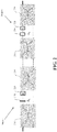
- FIG. 1 illustrates OCT system 101 including an optical source 102, a splitting element 104, a sample arm 106, a reference arm 108, variable delay system 112, and a detector 114.
- variable delay system 112 is located within reference arm 108. It should be understood, however, that variable delay system 112 may instead be located in sample arm 106.
- a simple delay line in sample arm 106 may take advantage of the light delivered to and reflected from the sample.
- sample arm 106 and reference arm 108 include optical waveguides such pattern or rib waveguides or optical fibers.
- OCT system 101 utilizing a variable delay system 112 is used for imaging a sample 110, according to an embodiment.
- Variable delay system 112 may be used to provide a variable delay to the light within OCT system 101.
- Light reflected from sample 110 and retuned by variable delay system 112 may be processed to form a high-resolution image of the sample, such as a high resolution three-dimensional volumetric image.
- the terms "electromagnetic radiation,” “light,” and “beam of radiation” are all used to describe the same electromagnetic signals propagating through the various described elements and systems.
- all of the components of OCT system 101 are integrated onto a planar lightwave circuit (PLC).
- PLC planar lightwave circuit
- at least all the components within variable delay system 112 are integrated on the same substrate of a PLC.
- Other implementations may be considered as well, such as, for example, fiber optic systems, free-space optical systems, photonic crystal systems, etc.
- OCT system 101 may include any number of other optical elements not shown for the sake of clarity.
- OCT system 101 may include mirrors, lenses, gratings, splitters, micromechanical elements, etc., along the paths of sample arm 106 or reference arm 108.
- OCT system 101 may include various modulating elements configured to suppress contributions of interference signals generated in non-active optical paths.
- OCT system 101 may include MEMS (Micro Electro Mechanical Systems), which apply an additional physical lateral scan to the beams.
- An optical element in the path of the light may be displaced by electromechanical actuators (e.g. based on thermal expansion, piezoelectric or electrostatic force) that are integrated by means of microfabrication techniques.
- Splitting element 104 is used to direct light received from optical source 102 to both sample arm 106 and reference arm 108.
- Splitting element 104 may be, for example, a bi-directional coupler, an optical splitter, or any other modulating optical device that converts a single beam of light into two or more beams of light.
- Sample 110 may be any suitable sample to be imaged, such as tissue.
- the light scans at a certain depth within sample 110 and the scattered radiation is collected back into sample arm 106.
- the scattered radiation is collected back into a different waveguide than the transmitting waveguide.
- the scan depth may be chosen via the delay imposed on the light within variable delay system 112.
- Variable delay system 112 may include one or more multiplexing units, with each unit differentiating the light among a plurality of optical channels. More details regarding the various multiplexing units are discussed herein.
- Light within sample arm 106 and reference arm 108 is recombined before being received at detector 114.
- the light is recombined by splitting element 104.
- the light is recombined at a different optical coupling element than splitting element 104.
- OCT system 101 may provide a distribution of the delay needed in different components, segmenting the axial scanning into Frequency Division Multiplexing (FDM) channels. Thus, OCT system 101 may simultaneously scan a sample at a plurality of axial depths. As a result, OCT system 101 may optimize bandwidth and maximum delay for the TD-OCT variable delay components.
- optical source 102 provides broadband light and variable delay system 112 separates the electrical spectrum of the detected signal into distinct channels that axially scan a sample at distinct axial scanning depth ranges and distinct frequency ranges.
- the OCT system may be configured as either a reflective system or a transmissive system.
- the OCT system 101 illustrated in FIG. 1 is configured as a reflective system, i.e. , the detection light is light reflected from the sample.
- a similar OCT system 501 may be configured as a transmissive system, i.e. , the detection light is light transmitted through the sample, as illustrated in FIG. 5 .
- the transmissive configuration of FIG. 5 illustrates OCT system 501 including an optical source 502, a first splitting element 504, a sample arm 506, a reference arm 508, variable delay system 512, and a detector 514.
- OCT system 501 may include a second splitting element 505 to direct the transmitted light and the light from variable delay system 512 to detector 514.
- a second splitting element 505 to direct the transmitted light and the light from variable delay system 512 to detector 514.
- FIG. 2 illustrates an example frequency domain modulation scheme of n number of stages.
- the modulation scheme presented here mainly refers to the reference arm, but a similar approach can be used in the sample arm.
- Each stage may include couplers 216, group delay elements 218, and group delay modulators 220.
- the stages are coupled together to form an interferometric network.
- the interferometric network divides the axial scanning range into 2" channels.
- Each one of the stages may have different delays ⁇ n so that the variable delay line in the sample arm can constructively interfere with reference arm at different depths. Varying the group delay of the light corresponds to varying a scan depth within the sample under study. If the stages are arranged in series, the delay needed by a single stage or section is much smaller than the one required by the entire system delay using this architecture and modulation scheme.
- exemplary modulation schemes allow for modulator bandwidth optimization.
- frequencies of phase modulation signals applied to the group delay modulators 220 are all the same and equal to the one applied into a delay line in the sample arm.
- Such phase modulation signals must be inverted with respect to the sample arm signal since the direction of their effect in the axial scanning is opposite.
- a frequency domain modulation scheme of 2 n channels is obtained (where n is the number of modulator stages or sections).
- couplers 216 may be optical couplers, such as 2 x 2 fiber optic couplers.
- three couplers may be used in series for a total of eight channels. Each channel may be used to scan a sample at a different axial depth. The information from each channel may be extracted and processed to form an image of the sample.
- Group delay elements 218 add a group delay in each stage to their respective portion of the optical path. An optical channel having a desired delay may then be formed by adding appropriate delays together along the optical path.
- group delays introduced by group delay elements 218 are fixed.
- Group delay modulators 220 induce a relative change of group delay in each stage such that the combined effect of group delay elements and group delay modulators of a particular optical path corresponds to a distinct axial scanning depth in a sample. The goal is to produce a plurality of possible optical channels, each with a different total group delay. In this manner, a desired group delay can be implemented in the OCT system to image different depths without moving parts.
- each of these optical channels is modulated using a characteristic frequency.
- Group delay elements 218 may be implemented in a variety of appropriate ways, such as by including waveguide segments of different lengths to physically increase the length of a particular optical path.
- each group delay element 218 induces a distinct group delay and the group delay elements 218 are arranged in increasing or decreasing order.
- group delay modulators 220 may be thermo-optic modulators.
- the thermo-optic modulators may be of the type described in WIPO Patent Application Publication No. 2013/001032 A1.
- thermo-optic modulators may modulate a beam of radiation by varying the refractive index of a waveguide carrying the beam of radiation.
- FIG. 6 illustrates a multi-stage network for implementing the proposed modulation scheme with fixed group delay elements 618 and group delay modulators 620 in different paths in each stage of the OCT system.
- fixed group delay elements 618 are in a first set of paths that are optically coupled in series in the reference arm, while group delay modulators are in a second set of paths optically coupled in series in the sample arm.
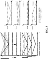
- FIG. 3 illustrates an example embodiment of a delay line modulation scheme, with group delay ( ⁇ g ) resulting from an example embodiment of a three-stage modulation scheme.
- Delay waveforms from the sample arm delay line and reference modulators 1 to 3 are depicted on the right.
- the sample delay line scans up to 156.25 ⁇ m in air, while modulator delays vary from 19.53 ⁇ m to 78.12 ⁇ m.
- delay increases between channels may be uniform.
- modulator waveforms in the reference arm are inverted with respect to the one in the sample arm.
- the graphs on the left of Fig. 3 illustrate the effective group delay as a consequence of the combination of the sample and reference arm scanning. The largest group delay contribution comes from the delay element in the sample arm. While the additional group delay contributions come from the three modulation stages in the reference arm.
- the three-stage modulation scheme creates eight different channels with eight different Doppler frequencies.
- the example modulators' delay magnitude was chosen so that the Doppler frequencies of the channels are distant enough to be separated in a later processing step. Were it otherwise, inter-channel crosstalk would degrade the image quality of the OCT system.
- the Doppler frequency is related to the slope of the group delay shown in FIG. 3 .
- channel distribution may be that in which each modulator's delay amplitude should be more than twice the previous one.
- variable delay ranges applied to the modulators create a scanning overlap in some of the generated channels. This means that a particular depth of the sample may be scanned by multiple channels. Despite a loss in energy efficiency, the overlap between channels may be used to increase the signal-to-noise ratio (SNR) by averaging the overlapping signals.
- SNR signal-to-noise ratio
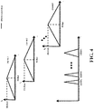
- FIG. 4 shows FDM channels' scanning depth and frequency spectrum.
- higher channels in Doppler frequency
- modulation Apart from increasing the central frequency for each channel, modulation also increases bandwidth. Higher frequency channels contribute to higher noise since the detection bandwidth increases. Consequently, higher frequency channels will show lower signal-to-noise ratio (SNR) or image quality compared to lower frequency channels.
- SNR signal-to-noise ratio
- An embodiment may, therefore, use low frequency channels for deeper areas and high frequency channels for swallow areas to equalize the overall image quality.
- an embodiment may use high frequency channels for deeper areas and high frequency channels for swallow areas.
Landscapes
- Physics & Mathematics (AREA)
- General Physics & Mathematics (AREA)
- Optics & Photonics (AREA)
- Engineering & Computer Science (AREA)
- Microelectronics & Electronic Packaging (AREA)
- General Health & Medical Sciences (AREA)
- Health & Medical Sciences (AREA)
- Nuclear Medicine, Radiotherapy & Molecular Imaging (AREA)
- Radiology & Medical Imaging (AREA)
- Signal Processing (AREA)
- Theoretical Computer Science (AREA)
- Investigating Or Analysing Materials By Optical Means (AREA)
- Instruments For Measurement Of Length By Optical Means (AREA)
- Length Measuring Devices By Optical Means (AREA)
Priority Applications (1)
| Application Number | Priority Date | Filing Date | Title |
|---|---|---|---|
| EP21186602.5A EP3943879A1 (en) | 2015-08-19 | 2016-08-19 | Distributed delay-line for low-coherence interferometry |
Applications Claiming Priority (3)
| Application Number | Priority Date | Filing Date | Title |
|---|---|---|---|
| US201562207049P | 2015-08-19 | 2015-08-19 | |
| US15/237,299 US10113858B2 (en) | 2015-08-19 | 2016-08-15 | Distributed delay-line for low-coherence interferometry |
| PCT/EP2016/069673 WO2017029386A1 (en) | 2015-08-19 | 2016-08-19 | Distributed delay-line for low-coherence interferometry |
Related Child Applications (1)
| Application Number | Title | Priority Date | Filing Date |
|---|---|---|---|
| EP21186602.5A Division EP3943879A1 (en) | 2015-08-19 | 2016-08-19 | Distributed delay-line for low-coherence interferometry |
Publications (2)
| Publication Number | Publication Date |
|---|---|
| EP3338051A1 EP3338051A1 (en) | 2018-06-27 |
| EP3338051B1 true EP3338051B1 (en) | 2021-07-21 |
Family
ID=56801532
Family Applications (2)
| Application Number | Title | Priority Date | Filing Date |
|---|---|---|---|
| EP16757209.8A Active EP3338051B1 (en) | 2015-08-19 | 2016-08-19 | Distributed delay-line for low-coherence interferometry |
| EP21186602.5A Pending EP3943879A1 (en) | 2015-08-19 | 2016-08-19 | Distributed delay-line for low-coherence interferometry |
Family Applications After (1)
| Application Number | Title | Priority Date | Filing Date |
|---|---|---|---|
| EP21186602.5A Pending EP3943879A1 (en) | 2015-08-19 | 2016-08-19 | Distributed delay-line for low-coherence interferometry |
Country Status (9)
| Country | Link |
|---|---|
| US (1) | US10113858B2 (enExample) |
| EP (2) | EP3338051B1 (enExample) |
| JP (1) | JP6951322B2 (enExample) |
| CN (1) | CN108139200A (enExample) |
| AU (1) | AU2016309769A1 (enExample) |
| BR (1) | BR112018003143A2 (enExample) |
| CA (1) | CA2995744A1 (enExample) |
| ES (1) | ES2885867T3 (enExample) |
| WO (1) | WO2017029386A1 (enExample) |
Families Citing this family (5)
| Publication number | Priority date | Publication date | Assignee | Title |
|---|---|---|---|---|
| US7318035B2 (en) | 2003-05-08 | 2008-01-08 | Dolby Laboratories Licensing Corporation | Audio coding systems and methods using spectral component coupling and spectral component regeneration |
| TWI497485B (zh) | 2004-08-25 | 2015-08-21 | Dolby Lab Licensing Corp | 用以重塑經合成輸出音訊信號之時域包絡以更接近輸入音訊信號之時域包絡的方法 |
| WO2018055605A1 (en) | 2016-09-26 | 2018-03-29 | Ixa Amc Office / Academic Medical Center | High-resolution integrated-optics-based spectrometer |
| EP3516325B1 (en) * | 2016-09-26 | 2021-12-15 | Ixa Amc Office / Academic Medical Center | Single-chip optical coherence tomography device |
| GB2598538A (en) * | 2020-05-18 | 2022-03-09 | Univ Loughborough | Method and apparatus for measuring distance |
Family Cites Families (17)
| Publication number | Priority date | Publication date | Assignee | Title |
|---|---|---|---|---|
| US5402256A (en) | 1994-03-31 | 1995-03-28 | At&T Corp. | Optical time slot interchanger apparatus and method of operation |
| WO1998043068A1 (en) | 1997-03-26 | 1998-10-01 | Kowa Company, Ltd. | Optical measuring instrument |
| WO2002071042A2 (en) * | 2001-01-29 | 2002-09-12 | Izatt Joseph A | Frequency-encoded parallel oct and associated systems and methods |
| US6654127B2 (en) | 2001-03-01 | 2003-11-25 | Carl Zeiss Ophthalmic Systems, Inc. | Optical delay line |
| WO2004111929A2 (en) * | 2003-05-28 | 2004-12-23 | Duke University | Improved system for fourier domain optical coherence tomography |
| RU2273823C1 (ru) * | 2004-08-18 | 2006-04-10 | Валентин Михайлович Геликонов | Интерферометрическое устройство (варианты) |
| ES2599317T3 (es) * | 2006-01-19 | 2017-02-01 | Optovue, Inc. | Tomador de imágenes de tomografía de coherencia óptica de dominio de Fourier |
| JP5006933B2 (ja) * | 2008-01-10 | 2012-08-22 | 日本電信電話株式会社 | 光遅延干渉回路 |
| US20120022360A1 (en) * | 2008-03-28 | 2012-01-26 | Volcano Corporation | Methods for intravascular imaging and flushing |
| WO2010011656A1 (en) | 2008-07-21 | 2010-01-28 | Optovue, Inc. | Extended range imaging |
| US8467858B2 (en) * | 2009-04-29 | 2013-06-18 | Tomophase Corporation | Image-guided thermotherapy based on selective tissue thermal treatment |
| TWI480513B (zh) * | 2009-12-04 | 2015-04-11 | Raydium Semiconductor Corp | 光學同調斷層檢測裝置及其運作方法 |
| ES2415555B2 (es) * | 2011-05-20 | 2014-07-09 | Medlumics, S.L. | Dispositivo de barrido para interferometría de baja coherencia. |
| ES2396391B2 (es) * | 2011-06-28 | 2014-12-04 | Medlumics, S.L. | Dispositivo de retardo óptico variable para interferometría de baja coherencia. |
| US9062960B2 (en) * | 2012-02-07 | 2015-06-23 | Medlumics S.L. | Flexible waveguides for optical coherence tomography |
| US9113782B2 (en) | 2012-06-01 | 2015-08-25 | Joshua Noel Hogan | Multiple reference OCT system |
| US9310185B2 (en) | 2013-06-12 | 2016-04-12 | Medlumics, S.L. | Electro-optical silicon-based phase modulator with null residual amplitude modulation |
-
2016
- 2016-08-15 US US15/237,299 patent/US10113858B2/en active Active
- 2016-08-19 JP JP2018508638A patent/JP6951322B2/ja active Active
- 2016-08-19 AU AU2016309769A patent/AU2016309769A1/en not_active Abandoned
- 2016-08-19 WO PCT/EP2016/069673 patent/WO2017029386A1/en not_active Ceased
- 2016-08-19 ES ES16757209T patent/ES2885867T3/es active Active
- 2016-08-19 CN CN201680059123.XA patent/CN108139200A/zh active Pending
- 2016-08-19 CA CA2995744A patent/CA2995744A1/en not_active Abandoned
- 2016-08-19 EP EP16757209.8A patent/EP3338051B1/en active Active
- 2016-08-19 BR BR112018003143A patent/BR112018003143A2/pt not_active Application Discontinuation
- 2016-08-19 EP EP21186602.5A patent/EP3943879A1/en active Pending
Non-Patent Citations (1)
| Title |
|---|
| None * |
Also Published As
| Publication number | Publication date |
|---|---|
| EP3338051A1 (en) | 2018-06-27 |
| CA2995744A1 (en) | 2017-02-23 |
| BR112018003143A2 (pt) | 2018-09-18 |
| AU2016309769A1 (en) | 2018-03-15 |
| CN108139200A (zh) | 2018-06-08 |
| US20170052016A1 (en) | 2017-02-23 |
| JP6951322B2 (ja) | 2021-10-20 |
| ES2885867T3 (es) | 2021-12-15 |
| EP3943879A1 (en) | 2022-01-26 |
| WO2017029386A1 (en) | 2017-02-23 |
| US10113858B2 (en) | 2018-10-30 |
| JP2018531636A (ja) | 2018-11-01 |
Similar Documents
| Publication | Publication Date | Title |
|---|---|---|
| EP3338051B1 (en) | Distributed delay-line for low-coherence interferometry | |
| EP2710327B1 (en) | Scanning device for low coherence interferometry | |
| EP2725966B1 (en) | Integrated delay line for optical coherence tomography | |
| AU2012260954A1 (en) | Scanning device for low coherence interferometry | |
| JP5817022B2 (ja) | 光合波器及びこの光合波器を用いた画像投影装置 | |
| WO2018209339A1 (en) | Space division multiplexing optical coherence tomography using an integrated photonic device | |
| EP3882606B1 (en) | Integrated system for active equalization of chromatic dispersion | |
| EP3325915B1 (en) | High-speed optical coherence tomography using multiple interferometers with suppressed multiple scattering cross-talk | |
| US6892003B2 (en) | Variable dispersion compensator and optical transmission system | |
| US6659614B2 (en) | Variable dispersion compensator and optical transmission system | |
| EP1511133B1 (en) | Multi-wavelength light source apparatus | |
| EP4286918A1 (en) | Display device | |
| HK40060895A (en) | Integrated system for active equalization of chromatic dispersion | |
| JP2018205646A (ja) | 2光波の位相調整装置 |
Legal Events
| Date | Code | Title | Description |
|---|---|---|---|
| STAA | Information on the status of an ep patent application or granted ep patent |
Free format text: STATUS: THE INTERNATIONAL PUBLICATION HAS BEEN MADE |
|
| PUAI | Public reference made under article 153(3) epc to a published international application that has entered the european phase |
Free format text: ORIGINAL CODE: 0009012 |
|
| STAA | Information on the status of an ep patent application or granted ep patent |
Free format text: STATUS: REQUEST FOR EXAMINATION WAS MADE |
|
| 17P | Request for examination filed |
Effective date: 20180309 |
|
| AK | Designated contracting states |
Kind code of ref document: A1 Designated state(s): AL AT BE BG CH CY CZ DE DK EE ES FI FR GB GR HR HU IE IS IT LI LT LU LV MC MK MT NL NO PL PT RO RS SE SI SK SM TR |
|
| AX | Request for extension of the european patent |
Extension state: BA ME |
|
| DAV | Request for validation of the european patent (deleted) | ||
| DAX | Request for extension of the european patent (deleted) | ||
| STAA | Information on the status of an ep patent application or granted ep patent |
Free format text: STATUS: EXAMINATION IS IN PROGRESS |
|
| 17Q | First examination report despatched |
Effective date: 20190515 |
|
| RAP1 | Party data changed (applicant data changed or rights of an application transferred) |
Owner name: MEDLUMICS S.L. |
|
| GRAP | Despatch of communication of intention to grant a patent |
Free format text: ORIGINAL CODE: EPIDOSNIGR1 |
|
| STAA | Information on the status of an ep patent application or granted ep patent |
Free format text: STATUS: GRANT OF PATENT IS INTENDED |
|
| RIC1 | Information provided on ipc code assigned before grant |
Ipc: G02B 6/28 20060101ALI20210210BHEP Ipc: A61B 3/10 20060101ALN20210210BHEP Ipc: G02B 6/12 20060101ALI20210210BHEP Ipc: G02B 6/293 20060101ALI20210210BHEP Ipc: G01B 9/02 20060101AFI20210210BHEP |
|
| INTG | Intention to grant announced |
Effective date: 20210304 |
|
| RIC1 | Information provided on ipc code assigned before grant |
Ipc: G02B 6/12 20060101ALI20210219BHEP Ipc: G01B 9/02 20060101AFI20210219BHEP Ipc: A61B 3/10 20060101ALN20210219BHEP Ipc: G02B 6/28 20060101ALI20210219BHEP Ipc: G02B 6/293 20060101ALI20210219BHEP |
|
| GRAS | Grant fee paid |
Free format text: ORIGINAL CODE: EPIDOSNIGR3 |
|
| GRAA | (expected) grant |
Free format text: ORIGINAL CODE: 0009210 |
|
| STAA | Information on the status of an ep patent application or granted ep patent |
Free format text: STATUS: THE PATENT HAS BEEN GRANTED |
|
| AK | Designated contracting states |
Kind code of ref document: B1 Designated state(s): AL AT BE BG CH CY CZ DE DK EE ES FI FR GB GR HR HU IE IS IT LI LT LU LV MC MK MT NL NO PL PT RO RS SE SI SK SM TR |
|
| REG | Reference to a national code |
Ref country code: GB Ref legal event code: FG4D |
|
| REG | Reference to a national code |
Ref country code: CH Ref legal event code: EP |
|
| REG | Reference to a national code |
Ref country code: DE Ref legal event code: R096 Ref document number: 602016060925 Country of ref document: DE |
|
| REG | Reference to a national code |
Ref country code: AT Ref legal event code: REF Ref document number: 1412977 Country of ref document: AT Kind code of ref document: T Effective date: 20210815 |
|
| REG | Reference to a national code |
Ref country code: IE Ref legal event code: FG4D |
|
| REG | Reference to a national code |
Ref country code: NL Ref legal event code: FP |
|
| REG | Reference to a national code |
Ref country code: LT Ref legal event code: MG9D |
|
| REG | Reference to a national code |
Ref country code: ES Ref legal event code: FG2A Ref document number: 2885867 Country of ref document: ES Kind code of ref document: T3 Effective date: 20211215 Ref country code: AT Ref legal event code: MK05 Ref document number: 1412977 Country of ref document: AT Kind code of ref document: T Effective date: 20210721 |
|
| PG25 | Lapsed in a contracting state [announced via postgrant information from national office to epo] |
Ref country code: AT Free format text: LAPSE BECAUSE OF FAILURE TO SUBMIT A TRANSLATION OF THE DESCRIPTION OR TO PAY THE FEE WITHIN THE PRESCRIBED TIME-LIMIT Effective date: 20210721 Ref country code: BG Free format text: LAPSE BECAUSE OF FAILURE TO SUBMIT A TRANSLATION OF THE DESCRIPTION OR TO PAY THE FEE WITHIN THE PRESCRIBED TIME-LIMIT Effective date: 20211021 Ref country code: LT Free format text: LAPSE BECAUSE OF FAILURE TO SUBMIT A TRANSLATION OF THE DESCRIPTION OR TO PAY THE FEE WITHIN THE PRESCRIBED TIME-LIMIT Effective date: 20210721 Ref country code: HR Free format text: LAPSE BECAUSE OF FAILURE TO SUBMIT A TRANSLATION OF THE DESCRIPTION OR TO PAY THE FEE WITHIN THE PRESCRIBED TIME-LIMIT Effective date: 20210721 Ref country code: FI Free format text: LAPSE BECAUSE OF FAILURE TO SUBMIT A TRANSLATION OF THE DESCRIPTION OR TO PAY THE FEE WITHIN THE PRESCRIBED TIME-LIMIT Effective date: 20210721 Ref country code: PT Free format text: LAPSE BECAUSE OF FAILURE TO SUBMIT A TRANSLATION OF THE DESCRIPTION OR TO PAY THE FEE WITHIN THE PRESCRIBED TIME-LIMIT Effective date: 20211122 Ref country code: NO Free format text: LAPSE BECAUSE OF FAILURE TO SUBMIT A TRANSLATION OF THE DESCRIPTION OR TO PAY THE FEE WITHIN THE PRESCRIBED TIME-LIMIT Effective date: 20211021 Ref country code: SE Free format text: LAPSE BECAUSE OF FAILURE TO SUBMIT A TRANSLATION OF THE DESCRIPTION OR TO PAY THE FEE WITHIN THE PRESCRIBED TIME-LIMIT Effective date: 20210721 Ref country code: RS Free format text: LAPSE BECAUSE OF FAILURE TO SUBMIT A TRANSLATION OF THE DESCRIPTION OR TO PAY THE FEE WITHIN THE PRESCRIBED TIME-LIMIT Effective date: 20210721 |
|
| PG25 | Lapsed in a contracting state [announced via postgrant information from national office to epo] |
Ref country code: PL Free format text: LAPSE BECAUSE OF FAILURE TO SUBMIT A TRANSLATION OF THE DESCRIPTION OR TO PAY THE FEE WITHIN THE PRESCRIBED TIME-LIMIT Effective date: 20210721 Ref country code: LV Free format text: LAPSE BECAUSE OF FAILURE TO SUBMIT A TRANSLATION OF THE DESCRIPTION OR TO PAY THE FEE WITHIN THE PRESCRIBED TIME-LIMIT Effective date: 20210721 |
|
| REG | Reference to a national code |
Ref country code: DE Ref legal event code: R097 Ref document number: 602016060925 Country of ref document: DE Ref country code: BE Ref legal event code: MM Effective date: 20210831 |
|
| PG25 | Lapsed in a contracting state [announced via postgrant information from national office to epo] |
Ref country code: DK Free format text: LAPSE BECAUSE OF FAILURE TO SUBMIT A TRANSLATION OF THE DESCRIPTION OR TO PAY THE FEE WITHIN THE PRESCRIBED TIME-LIMIT Effective date: 20210721 |
|
| PLBE | No opposition filed within time limit |
Free format text: ORIGINAL CODE: 0009261 |
|
| STAA | Information on the status of an ep patent application or granted ep patent |
Free format text: STATUS: NO OPPOSITION FILED WITHIN TIME LIMIT |
|
| PG25 | Lapsed in a contracting state [announced via postgrant information from national office to epo] |
Ref country code: SM Free format text: LAPSE BECAUSE OF FAILURE TO SUBMIT A TRANSLATION OF THE DESCRIPTION OR TO PAY THE FEE WITHIN THE PRESCRIBED TIME-LIMIT Effective date: 20210721 Ref country code: SK Free format text: LAPSE BECAUSE OF FAILURE TO SUBMIT A TRANSLATION OF THE DESCRIPTION OR TO PAY THE FEE WITHIN THE PRESCRIBED TIME-LIMIT Effective date: 20210721 Ref country code: RO Free format text: LAPSE BECAUSE OF FAILURE TO SUBMIT A TRANSLATION OF THE DESCRIPTION OR TO PAY THE FEE WITHIN THE PRESCRIBED TIME-LIMIT Effective date: 20210721 Ref country code: MC Free format text: LAPSE BECAUSE OF FAILURE TO SUBMIT A TRANSLATION OF THE DESCRIPTION OR TO PAY THE FEE WITHIN THE PRESCRIBED TIME-LIMIT Effective date: 20210721 Ref country code: LU Free format text: LAPSE BECAUSE OF NON-PAYMENT OF DUE FEES Effective date: 20210819 Ref country code: EE Free format text: LAPSE BECAUSE OF FAILURE TO SUBMIT A TRANSLATION OF THE DESCRIPTION OR TO PAY THE FEE WITHIN THE PRESCRIBED TIME-LIMIT Effective date: 20210721 Ref country code: CZ Free format text: LAPSE BECAUSE OF FAILURE TO SUBMIT A TRANSLATION OF THE DESCRIPTION OR TO PAY THE FEE WITHIN THE PRESCRIBED TIME-LIMIT Effective date: 20210721 Ref country code: AL Free format text: LAPSE BECAUSE OF FAILURE TO SUBMIT A TRANSLATION OF THE DESCRIPTION OR TO PAY THE FEE WITHIN THE PRESCRIBED TIME-LIMIT Effective date: 20210721 |
|
| 26N | No opposition filed |
Effective date: 20220422 |
|
| PG25 | Lapsed in a contracting state [announced via postgrant information from national office to epo] |
Ref country code: IT Free format text: LAPSE BECAUSE OF FAILURE TO SUBMIT A TRANSLATION OF THE DESCRIPTION OR TO PAY THE FEE WITHIN THE PRESCRIBED TIME-LIMIT Effective date: 20210721 Ref country code: IE Free format text: LAPSE BECAUSE OF NON-PAYMENT OF DUE FEES Effective date: 20210819 Ref country code: BE Free format text: LAPSE BECAUSE OF NON-PAYMENT OF DUE FEES Effective date: 20210831 |
|
| PG25 | Lapsed in a contracting state [announced via postgrant information from national office to epo] |
Ref country code: HU Free format text: LAPSE BECAUSE OF FAILURE TO SUBMIT A TRANSLATION OF THE DESCRIPTION OR TO PAY THE FEE WITHIN THE PRESCRIBED TIME-LIMIT; INVALID AB INITIO Effective date: 20160819 |
|
| P01 | Opt-out of the competence of the unified patent court (upc) registered |
Effective date: 20230507 |
|
| PG25 | Lapsed in a contracting state [announced via postgrant information from national office to epo] |
Ref country code: CY Free format text: LAPSE BECAUSE OF FAILURE TO SUBMIT A TRANSLATION OF THE DESCRIPTION OR TO PAY THE FEE WITHIN THE PRESCRIBED TIME-LIMIT Effective date: 20210721 |
|
| PG25 | Lapsed in a contracting state [announced via postgrant information from national office to epo] |
Ref country code: GR Free format text: LAPSE BECAUSE OF FAILURE TO SUBMIT A TRANSLATION OF THE DESCRIPTION OR TO PAY THE FEE WITHIN THE PRESCRIBED TIME-LIMIT Effective date: 20210721 |
|
| PG25 | Lapsed in a contracting state [announced via postgrant information from national office to epo] |
Ref country code: MK Free format text: LAPSE BECAUSE OF FAILURE TO SUBMIT A TRANSLATION OF THE DESCRIPTION OR TO PAY THE FEE WITHIN THE PRESCRIBED TIME-LIMIT Effective date: 20210721 |
|
| PG25 | Lapsed in a contracting state [announced via postgrant information from national office to epo] |
Ref country code: MT Free format text: LAPSE BECAUSE OF FAILURE TO SUBMIT A TRANSLATION OF THE DESCRIPTION OR TO PAY THE FEE WITHIN THE PRESCRIBED TIME-LIMIT Effective date: 20210721 |
|
| PGFP | Annual fee paid to national office [announced via postgrant information from national office to epo] |
Ref country code: NL Payment date: 20250821 Year of fee payment: 10 |
|
| PGFP | Annual fee paid to national office [announced via postgrant information from national office to epo] |
Ref country code: ES Payment date: 20250917 Year of fee payment: 10 |
|
| PGFP | Annual fee paid to national office [announced via postgrant information from national office to epo] |
Ref country code: DE Payment date: 20250819 Year of fee payment: 10 |
|
| PGFP | Annual fee paid to national office [announced via postgrant information from national office to epo] |
Ref country code: GB Payment date: 20250822 Year of fee payment: 10 |
|
| PGFP | Annual fee paid to national office [announced via postgrant information from national office to epo] |
Ref country code: FR Payment date: 20250821 Year of fee payment: 10 |
|
| PGFP | Annual fee paid to national office [announced via postgrant information from national office to epo] |
Ref country code: CH Payment date: 20250901 Year of fee payment: 10 |
|
| REG | Reference to a national code |
Ref country code: CH Ref legal event code: R18 Free format text: ST27 STATUS EVENT CODE: U-0-0-R10-R18 (AS PROVIDED BY THE NATIONAL OFFICE) Effective date: 20251105 |
|
| PG25 | Lapsed in a contracting state [announced via postgrant information from national office to epo] |
Ref country code: TR Free format text: LAPSE BECAUSE OF FAILURE TO SUBMIT A TRANSLATION OF THE DESCRIPTION OR TO PAY THE FEE WITHIN THE PRESCRIBED TIME-LIMIT Effective date: 20210721 |