EP3336886A1 - Semiconductor wafer dicing method - Google Patents
Semiconductor wafer dicing method Download PDFInfo
- Publication number
- EP3336886A1 EP3336886A1 EP17197172.4A EP17197172A EP3336886A1 EP 3336886 A1 EP3336886 A1 EP 3336886A1 EP 17197172 A EP17197172 A EP 17197172A EP 3336886 A1 EP3336886 A1 EP 3336886A1
- Authority
- EP
- European Patent Office
- Prior art keywords
- wafer
- saw
- sides
- thickness
- cut
- Prior art date
- Legal status (The legal status is an assumption and is not a legal conclusion. Google has not performed a legal analysis and makes no representation as to the accuracy of the status listed.)
- Pending
Links
Images

Classifications
-
- H—ELECTRICITY
- H10—SEMICONDUCTOR DEVICES; ELECTRIC SOLID-STATE DEVICES NOT OTHERWISE PROVIDED FOR
- H10P—GENERIC PROCESSES OR APPARATUS FOR THE MANUFACTURE OR TREATMENT OF DEVICES COVERED BY CLASS H10
- H10P54/00—Cutting or separating of wafers, substrates or parts of devices
-
- H—ELECTRICITY
- H10—SEMICONDUCTOR DEVICES; ELECTRIC SOLID-STATE DEVICES NOT OTHERWISE PROVIDED FOR
- H10P—GENERIC PROCESSES OR APPARATUS FOR THE MANUFACTURE OR TREATMENT OF DEVICES COVERED BY CLASS H10
- H10P52/00—Grinding, lapping or polishing of wafers, substrates or parts of devices
Definitions
- the present invention is directed to semiconductor wafers and, more particularly, to a method of dicing semiconductor wafers.
- FIG. 1 shows an example of a bowed wafer 10 having a plurality of integrated circuit dies 12 formed thereon. As can be seen, the wafer 10 is warped or includes a bow 14. Bowed wafers mounted to a tape experience high residual stress, such that when dicing the wafer, die chipping may occur, which decreases yield and therefore is costly.
- the present invention provides a method of dicing or singulating a semiconductor wafer into a plurality of dies, where the wafer comprises a plurality of dies arranged in a matrix on the wafer.
- the dies are separated by saw streets that run in first and second directions, with the second direction being perpendicular to the first direction.
- the method includes the steps of cutting along the saw streets in the first direction on a first half of the wafer, cutting along the saw streets in the first direction on a second half of the wafer opposite to the first half, and step-cutting along the saw streets in the second direction such that all of the dies are separated from each other, and the sides of the dies parallel to the first direction are flat and the sides of the dies perpendicular to the first direction are stepped.
- the present invention provides a semiconductor die that has been cut from a wafer.
- the die has an integrated circuit formed therein, and includes a top planar surface, a bottom planar surface opposite to the top planar surface, first and second sides that extend between the top and bottom surfaces, wherein the first and second sides are opposite to each other and are flat, and third and fourth sides that extend between the top and bottom surfaces, wherein the third and fourth sides are opposite to each other, and wherein the third and fourth sides are stepped such that a length of the bottom surface is greater than a length of the top surface.
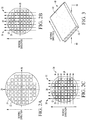
- FIG. 2A a top plan view of a wafer 20 including an array of semiconductor dies 22 is shown.
- the dies 22 are formed in rows and columns and separated by saw streets, as is known by those of skill in the art.
- the wafer 20 is generally circular and typically includes one straight edge 24 used to orient the wafer 20. As previously discussed, as wafers become thinner and larger, they can be subject to warping or bowing. While the invention disclosed herein is particularly useful for bowed wafers, it will be understood by those of skill in the art that the invention may be practiced on wafers that are not bowed.In FIG. 2A , the example wafer 20 is bowed and the bowing is in the direction shown by the arrow on the left side of the wafer.
- the wafer 20 is secured to a dicing tape with a film frame carrier.
- the wafer may be secured to the carrier with an adhesive and/or with vacuum pressure, as is known in the art.
- Sece dicing tapes and film frame carriers are known in the art, and modifications to known carriers are not required in order to practice the present invention, further description thereof is not necessary for a complete understanding of the present invention.
- a first cut 26 is made along a saw street in a first direction and through a center of the wafer 20, which divides the wafer 20 into first and second halves.
- the first cut 26 is made perpendicular to the direction of the bowing and extends entirely through the wafer 20.
- a second cut 28 is made along a saw street that is perpendicular to the first cut (and therefore in the direction of the bowing).
- the second cut 28 also passes through the center of the wafer 20, and thus the wafer 20 is separated into quarters.
- the first and second cuts 26 and 28 are performed using the same saw blade and cut to the same depth. The first and second cuts 26 and 28 are believed to reduce residual stress on the wafer 20 caused by the bowing.
- FIG. 2B is a top plan view of the wafer 20 after being quartered by the first and second cuts 26 and 28.
- the wafer 20 is cut along the saw streets in the bowing direction on one side or a first half of the wafer 20 in a first step 30, and then cut along the saw streets in the bowing direction on the other or second, opposite half of the wafer 20 in a second step 32.
- the first and second steps are performed simultaneously.
- the cuts 30 are made using the same saw blade as was used for quartering the wafer 20, while the cuts 32 are made using a thinner saw blade or a saw blade with a smaller kerf.
- FIG. 2C is a top plan view of the wafer 20 illustrating a next step in which the wafer 20 is cut in a direction perpendicular to the bowing direction, after the cuts 30 and 32 are made in the bowing direction.
- the cuts perpendicular to the bowing are illustrated with arrows 34.
- the cuts 34 comprise step-cuts, and these step cuts separate the dies 22 from each other.
- the step-cutting comprises making a first cut along the saw streets in the direction perpendicular to the bowing direction with the thicker saw blade to a first depth, and then making a second cut along the saw streets in the same direction with the thinner saw blade to a second depth, which is the depth required to cut through the wafer 20.
- the depth of the first cut made with the thicker saw blade ranges from about 50% to 80% of the wafer thickness, and preferable from 70% - 80% of the wafer thickness. Further, the first saw blade has a thickness ranging from about 20 to 25 um, and the second saw blade has a thickness ranging from 15 to 20 um, although it is understood that the different blade widths will be within the saw street or scribe lane of the wafer 20.
- Such size saw blades used for semiconductor wafer dicing are commercially available. Accordingingly, a die separated using the described method has sides parallel to the bowing direction that are flat and the sides perpendicular to the bowing direction that are stepped.
- FIG. 3 shows a semiconductor die 40 that has been cut from a wafer using the above-described method.
- the die 40 has a top planar surface 42, and a bottom planar surface opposite to the top planar surface.
- the die 40 also has first and second sides 44 that extend between the top and bottom surfaces.
- the first and second sides 44 are opposite to each other and are flat, as shown in FIG. 3 .
- the third and fourth sides 46 are opposite to each other, and are stepped such that a length of the bottom surface is greater than a length of the top surface.
- stepped sides have one step, and since the depth of the first cut, with the thicker saw blade is about 70-80% of the thickness of the wafer, then a distance from the top surface 42 to the step 48 is greater than a distance from the bottom surface to the step 48.
- the invention is applicable to all bowed wafers to attain dies with good chipping quality.
- Application of a step-cut perpendicular to direction of the bowing of the wafer bowing has been found to prevent severe back chipping.
Landscapes
- Dicing (AREA)
Abstract
A method of dicing a bowed or warped semiconductor wafer includes cutting along the saw streets in a first direction on a first half of the wafer, where the first direction is parallel to the bowing, cutting along the saw streets in the first direction on a second half of the wafer opposite to the first half, and step-cutting along the saw streets in the second direction, such that all of the dies are separated from each other, and the sides of the die in the bowing direction are flat and the sides of the die perpendicular to the bowing direction are stepped.
Description
- The present invention is directed to semiconductor wafers and, more particularly, to a method of dicing semiconductor wafers.
- Integrated circuit dies are formed on semiconductor wafers. Depending on the dimensions of the wafer and the processes and materials used for forming the dies on the wafer, as well as any environmental conditions to which the wafer may be exposed, the wafer may experience some warping or bowing. For example, some wafer bowing is inherent for wafers that embody deep trench technologies.
FIG. 1 shows an example of abowed wafer 10 having a plurality of integrated circuit dies 12 formed thereon. As can be seen, thewafer 10 is warped or includes abow 14. Bowed wafers mounted to a tape experience high residual stress, such that when dicing the wafer, die chipping may occur, which decreases yield and therefore is costly. - It would be advantageous to be able to singulate the dies formed on a wafer without excessive chipping, and thereby providing for better yield.
- The present invention is illustrated by way of example and is not limited by embodiments thereof shown in the accompanying figures, in which like references indicate similar elements. Elements in the figures are illustrated for simplicity and clarity and have not necessarily been drawn to scale.
-
FIG. 1 is a photograph of a bowed semiconductor wafer;FIGS. 2A, 2B and 2C are top plan views of a wafer illustrating the steps of wafer dicing in accordance with a preferred embodiment of the present invention; and -
FIG. 3 is an isometric view of an integrated circuit die cut from a semiconductor wafer in accordance with an embodiment of the present invention. - The present invention provides a method of dicing or singulating a semiconductor wafer into a plurality of dies, where the wafer comprises a plurality of dies arranged in a matrix on the wafer. The dies are separated by saw streets that run in first and second directions, with the second direction being perpendicular to the first direction. The method includes the steps of cutting along the saw streets in the first direction on a first half of the wafer, cutting along the saw streets in the first direction on a second half of the wafer opposite to the first half, and step-cutting along the saw streets in the second direction such that all of the dies are separated from each other, and the sides of the dies parallel to the first direction are flat and the sides of the dies perpendicular to the first direction are stepped.
- In another embodiment, the present invention provides a semiconductor die that has been cut from a wafer. The die has an integrated circuit formed therein, and includes a top planar surface, a bottom planar surface opposite to the top planar surface, first and second sides that extend between the top and bottom surfaces, wherein the first and second sides are opposite to each other and are flat, and third and fourth sides that extend between the top and bottom surfaces, wherein the third and fourth sides are opposite to each other, and wherein the third and fourth sides are stepped such that a length of the bottom surface is greater than a length of the top surface.
- Referring now to
FIG. 2A , a top plan view of awafer 20 including an array ofsemiconductor dies 22 is shown. Thedies 22 are formed in rows and columns and separated by saw streets, as is known by those of skill in the art. Thewafer 20 is generally circular and typically includes one straight edge 24 used to orient thewafer 20. As previously discussed, as wafers become thinner and larger, they can be subject to warping or bowing. While the invention disclosed herein is particularly useful for bowed wafers, it will be understood by those of skill in the art that the invention may be practiced on wafers that are not bowed.InFIG. 2A , theexample wafer 20 is bowed and the bowing is in the direction shown by the arrow on the left side of the wafer. - First, prior to dicing the
wafer 20, thewafer 20 is secured to a dicing tape with a film frame carrier.The wafer may be secured to the carrier with an adhesive and/or with vacuum pressure, as is known in the art.Since dicing tapes and film frame carriers are known in the art, and modifications to known carriers are not required in order to practice the present invention, further description thereof is not necessary for a complete understanding of the present invention. - In a first step, a
first cut 26 is made along a saw street in a first direction and through a center of thewafer 20, which divides thewafer 20 into first and second halves. In the presently preferred embodiment, thefirst cut 26 is made perpendicular to the direction of the bowing and extends entirely through thewafer 20. Then, asecond cut 28 is made along a saw street that is perpendicular to the first cut (and therefore in the direction of the bowing). Thesecond cut 28 also passes through the center of thewafer 20, and thus thewafer 20 is separated into quarters. In the presently preferred embodiment, the first andsecond cuts second cuts wafer 20 caused by the bowing. -
FIG. 2B is a top plan view of thewafer 20 after being quartered by the first andsecond cuts wafer 20 is cut along the saw streets in the bowing direction on one side or a first half of thewafer 20 in afirst step 30, and then cut along the saw streets in the bowing direction on the other or second, opposite half of thewafer 20 in asecond step 32. In the presently preferred embodiment, the first and second steps are performed simultaneously. Although not required, in the presently preferred embodiment, thecuts 30 are made using the same saw blade as was used for quartering thewafer 20, while thecuts 32 are made using a thinner saw blade or a saw blade with a smaller kerf. -
FIG. 2C is a top plan view of thewafer 20 illustrating a next step in which thewafer 20 is cut in a direction perpendicular to the bowing direction, after thecuts arrows 34. Thecuts 34 comprise step-cuts, and these step cuts separate thedies 22 from each other. The step-cutting comprises making a first cut along the saw streets in the direction perpendicular to the bowing direction with the thicker saw blade to a first depth, and then making a second cut along the saw streets in the same direction with the thinner saw blade to a second depth, which is the depth required to cut through thewafer 20. - The depth of the first cut made with the thicker saw blade ranges from about 50% to 80% of the wafer thickness, and preferable from 70% - 80% of the wafer thickness. Further, the first saw blade has a thickness ranging from about 20 to 25 um, and the second saw blade has a thickness ranging from 15 to 20 um, although it is understood that the different blade widths will be within the saw street or scribe lane of the
wafer 20. Such size saw blades used for semiconductor wafer dicing are commercially available.Accordingly, a die separated using the described method has sides parallel to the bowing direction that are flat and the sides perpendicular to the bowing direction that are stepped. -
FIG. 3 shows asemiconductor die 40 that has been cut from a wafer using the above-described method.The die 40 has a topplanar surface 42, and a bottom planar surface opposite to the top planar surface. The die 40 also has first andsecond sides 44 that extend between the top and bottom surfaces. The first andsecond sides 44 are opposite to each other and are flat, as shown inFIG. 3 . There also are third andfourth sides 46 that extend between the top and bottom surfaces. The third andfourth sides 46 are opposite to each other, and are stepped such that a length of the bottom surface is greater than a length of the top surface. Using the step-cut process described above forms stepped sides have one step, and since the depth of the first cut, with the thicker saw blade is about 70-80% of the thickness of the wafer, then a distance from thetop surface 42 to thestep 48 is greater than a distance from the bottom surface to thestep 48. - The invention is applicable to all bowed wafers to attain dies with good chipping quality. Application of a step-cut perpendicular to direction of the bowing of the wafer bowing has been found to prevent severe back chipping.
- In the foregoing specification, the invention has been described with reference to specific examples of embodiments of the invention. It will, however, be evident that various modifications and changes may be made therein without departing from the broader spirit and scope of the invention as set forth in the appended claims.
- In the claims, the words 'comprising', 'including', and 'having' do not exclude the presence of other elements or steps then those listed in a claim. The terms "a" or "an," as used herein, are defined as one or more than one.Also, the use of introductory phrases such as "at least one" and "one or more" in the claims should not be construed to imply that the introduction of another claim element by the indefinite articles "a" or "an" limits any particular claim containing such introduced claim element to inventions containing only one such element, even when the same claim includes the introductory phrases "one or more" or "at least one" and indefinite articles such as "a" or "an." The same holds true for the use of definite articles. Unless stated otherwise, terms such as "first" and "second" are used to arbitrarily distinguish between the elements such terms describe.Thus, these terms are not necessarily intended to indicate temporal or other prioritization of such elements. The fact that certain measures are recited in mutually different claims does not indicate that a combination of these measures cannot be used to advantage.
Claims (15)
- A method of dicing a semiconductor wafer, wherein the wafer comprises a plurality of dies arranged in a matrix on the wafer, wherein the dies are separated by saw streets that run in a first direction and a second direction perpendicular to the first direction, the method comprising:cutting along the saw streets in the first direction on a first half of the wafer;cutting along the saw streets in the first direction on a second half of the wafer opposite to the first half; andstep-cutting along the saw streets in the second direction, whereby all of the dies are separated from each other, and the sides of the dies parallel to the first direction are flat and the sides of the dies perpendicular to the first direction are stepped.
- The method of claim 1, wherein the step-cutting comprises making a first cut along the saw streets in the second direction with a first saw blade having a first thickness and to a first depth, and a second cut along the saw streets in the second direction with a second saw blade having a second thickness and to a second depth.
- The method of claims 1 or 2, wherein the first depth ranges from 70% to 80% of the wafer thickness.
- The method of any preceding claim, wherein the first saw blade has a thickness ranging from 20 to 25 um and the second saw blade has a thickness ranging from 15 to 20 um.
- The method of any preceding claim, wherein cutting along the saw streets in the first direction on the first half of the wafer is performed using a saw blade having a first thickness.
- The method of any preceding claim, wherein cutting along the saw streets in the first direction on the second half of the wafer is performed using a saw blade having a second thickness different from the first thickness and
wherein the first thickness is greater than the second thickness. - The method of any preceding claim, wherein the wafer is bowed in the first direction.
- The method of any preceding claim, further comprising, prior to cutting along the saw streets in the first direction on a first half of the wafer, making a first cut along a saw street in the second direction and through a center of the wafer to separate the wafer into the first and second halves.
- The method of claim 8, further comprising after making the first cut and before cutting along the saw streets in the first direction on the first half of the wafer, making a second cut along a saw street in the first direction and through the center of the wafer to separate the wafer into quarters.
- The method of any preceding claim, wherein prior to making the first cut, the wafer is secured to a dicing tape with a film frame carrier.
- The method of claim 10, wherein the wafer is secured to the carrier with an adhesive, or with vacuum pressure.
- A semiconductor die having an integrated circuit formed therein, comprising:a top planar surface;a bottom planar surface opposite to the top planar surface;first and second sides that extend between the top and bottom surfaces, wherein the first and second sides are opposite to each other and are flat; andthird and fourth sides that extend between the top and bottom surfaces, wherein the third and fourth sides are opposite to each other, and wherein the third and fourth sides are stepped such that a length of the bottom surface is greater than a length of the top surface.
- The semiconductor die of claim 12, wherein the stepped sides have one step.
- The semiconductor die of claims 12 or 13, wherein a distance from the top surface to the step is greater than a distance from the bottom surface to the step.
- The semiconductor die of claims 12 to 14, wherein a wafer from which the semiconductor die is cut is bowed and the first and second sides extend along the direction of the bow.
Applications Claiming Priority (1)
| Application Number | Priority Date | Filing Date | Title |
|---|---|---|---|
| US15/379,495 US10297500B2 (en) | 2016-12-15 | 2016-12-15 | Semiconductor wafer dicing method |
Publications (1)
| Publication Number | Publication Date |
|---|---|
| EP3336886A1 true EP3336886A1 (en) | 2018-06-20 |
Family
ID=60153107
Family Applications (1)
| Application Number | Title | Priority Date | Filing Date |
|---|---|---|---|
| EP17197172.4A Pending EP3336886A1 (en) | 2016-12-15 | 2017-10-18 | Semiconductor wafer dicing method |
Country Status (3)
| Country | Link |
|---|---|
| US (1) | US10297500B2 (en) |
| EP (1) | EP3336886A1 (en) |
| CN (1) | CN108231571A (en) |
Families Citing this family (3)
| Publication number | Priority date | Publication date | Assignee | Title |
|---|---|---|---|---|
| CN110625267A (en) * | 2019-08-22 | 2019-12-31 | 大族激光科技产业集团股份有限公司 | A method and laser device for processing a sapphire substrate LED wafer |
| JP2022108406A (en) * | 2021-01-13 | 2022-07-26 | 三菱電機株式会社 | Semiconductor chip, semiconductor device, and manufacturing method of semiconductor device |
| US20230042659A1 (en) * | 2021-08-03 | 2023-02-09 | Meta Platforms, Inc. | Complex photonics circuit fabrication |
Citations (3)
| Publication number | Priority date | Publication date | Assignee | Title |
|---|---|---|---|---|
| US20010024300A1 (en) * | 2000-03-27 | 2001-09-27 | Kabushiki Kaisha Toshiba | Sensor chip, image reading sensor, and electronic device |
| US20050006725A1 (en) * | 2003-05-16 | 2005-01-13 | Tetsuya Kurosawa | Semiconductor device and manufacturing method thereof |
| WO2012042292A1 (en) * | 2010-09-30 | 2012-04-05 | Freescale Semiconductor, Inc. | Methods for processing a semiconductor wafer, a semiconductor wafer and a semiconductor device |
Family Cites Families (11)
| Publication number | Priority date | Publication date | Assignee | Title |
|---|---|---|---|---|
| EP0678904A1 (en) | 1994-04-12 | 1995-10-25 | Lsi Logic Corporation | Multicut wafer saw process |
| US5609148A (en) | 1995-03-31 | 1997-03-11 | Siemens Aktiengesellschaft | Method and apparatus for dicing semiconductor wafers |
| US5718615A (en) | 1995-10-20 | 1998-02-17 | Boucher; John N. | Semiconductor wafer dicing method |
| US6136137A (en) | 1998-07-06 | 2000-10-24 | Micron Technology, Inc. | System and method for dicing semiconductor components |
| US6357330B1 (en) | 1999-01-07 | 2002-03-19 | Intel Corporation | Method and apparatus for cutting a wafer |
| US20020052169A1 (en) * | 2000-03-17 | 2002-05-02 | Krishna Vepa | Systems and methods to significantly reduce the grinding marks in surface grinding of semiconductor wafers |
| TWI223424B (en) | 2004-01-02 | 2004-11-01 | Advanced Semiconductor Eng | Process of cutting electrical packages |
| US9159595B2 (en) * | 2010-02-09 | 2015-10-13 | Suss Microtec Lithography Gmbh | Thin wafer carrier |
| JP2014093444A (en) * | 2012-11-05 | 2014-05-19 | Disco Abrasive Syst Ltd | Wafer processing method |
| US20150332970A1 (en) * | 2014-05-16 | 2015-11-19 | Wei-Sheng Lei | Carrier with thermally resistant film frame for supporting wafer during singulation |
| US20160148842A1 (en) * | 2014-11-24 | 2016-05-26 | Nxp B.V. | Dicing of low-k wafers |
-
2016
- 2016-12-15 US US15/379,495 patent/US10297500B2/en active Active
-
2017
- 2017-10-18 EP EP17197172.4A patent/EP3336886A1/en active Pending
- 2017-12-15 CN CN201711360171.5A patent/CN108231571A/en active Pending
Patent Citations (3)
| Publication number | Priority date | Publication date | Assignee | Title |
|---|---|---|---|---|
| US20010024300A1 (en) * | 2000-03-27 | 2001-09-27 | Kabushiki Kaisha Toshiba | Sensor chip, image reading sensor, and electronic device |
| US20050006725A1 (en) * | 2003-05-16 | 2005-01-13 | Tetsuya Kurosawa | Semiconductor device and manufacturing method thereof |
| WO2012042292A1 (en) * | 2010-09-30 | 2012-04-05 | Freescale Semiconductor, Inc. | Methods for processing a semiconductor wafer, a semiconductor wafer and a semiconductor device |
Also Published As
| Publication number | Publication date |
|---|---|
| US10297500B2 (en) | 2019-05-21 |
| US20180174907A1 (en) | 2018-06-21 |
| CN108231571A (en) | 2018-06-29 |
Similar Documents
| Publication | Publication Date | Title |
|---|---|---|
| KR960005047B1 (en) | Dicing Method of Compound Semiconductor Wafer | |
| US20160071770A1 (en) | Plasma etching and stealth dicing laser process | |
| US20130178006A1 (en) | Wafer dicing method and method of manufacturing light emitting device chips employing the same | |
| US11942369B2 (en) | Thin semiconductor package for notched semiconductor die | |
| CN109570783B (en) | Method and device for processing wafer by laser | |
| US10535588B2 (en) | Die with metallized sidewall and method of manufacturing | |
| US10297500B2 (en) | Semiconductor wafer dicing method | |
| US10607861B2 (en) | Die separation using adhesive-layer laser scribing | |
| US9543206B2 (en) | Wafer die separation | |
| US20050263854A1 (en) | Thick laser-scribed GaN-on-sapphire optoelectronic devices | |
| US9972535B2 (en) | Method of separating semiconductor dies from a semiconductor substrate, semiconductor substrate assembly and semiconductor die assembly | |
| KR20160054415A (en) | Method for manufacturing semiconductor piece | |
| US20160148842A1 (en) | Dicing of low-k wafers | |
| US10943886B2 (en) | Methods of forming semiconductor packages with back side metal | |
| US20120252142A1 (en) | Singulation and Strip Testing of No-Lead Integrated Circuit Packages Without Tape Frame | |
| US10957597B2 (en) | Semiconductor substrate die sawing singulation systems and methods | |
| JP2013161944A (en) | Dicing method | |
| US7179720B2 (en) | Pre-fabrication scribing | |
| KR102190861B1 (en) | Scribing method and scribing device | |
| WO2013150427A1 (en) | Led thin-film device partial singulation prior to substrate thinning or removal | |
| US10636707B2 (en) | Method of manufacturing a semiconductor device | |
| CN101095222B (en) | Method for producing semiconductor chips from a wafer | |
| US20160339603A1 (en) | Method for splitting circles | |
| JP2014165324A (en) | Method of working package substrate | |
| KR102327105B1 (en) | Method for manufacturing light emitting diode chip and light emitting diode chip |
Legal Events
| Date | Code | Title | Description |
|---|---|---|---|
| PUAI | Public reference made under article 153(3) epc to a published international application that has entered the european phase |
Free format text: ORIGINAL CODE: 0009012 |
|
| STAA | Information on the status of an ep patent application or granted ep patent |
Free format text: STATUS: THE APPLICATION HAS BEEN PUBLISHED |
|
| AK | Designated contracting states |
Kind code of ref document: A1 Designated state(s): AL AT BE BG CH CY CZ DE DK EE ES FI FR GB GR HR HU IE IS IT LI LT LU LV MC MK MT NL NO PL PT RO RS SE SI SK SM TR |
|
| AX | Request for extension of the european patent |
Extension state: BA ME |