EP3335347B1 - Harq-feedback-konfigurationstechniken für breitbandige drahtloskommunikationsnetzwerke - Google Patents
Harq-feedback-konfigurationstechniken für breitbandige drahtloskommunikationsnetzwerke Download PDFInfo
- Publication number
- EP3335347B1 EP3335347B1 EP15826211.3A EP15826211A EP3335347B1 EP 3335347 B1 EP3335347 B1 EP 3335347B1 EP 15826211 A EP15826211 A EP 15826211A EP 3335347 B1 EP3335347 B1 EP 3335347B1
- Authority
- EP
- European Patent Office
- Prior art keywords
- harq feedback
- pucch
- hfci
- field
- format
- Prior art date
- Legal status (The legal status is an assumption and is not a legal conclusion. Google has not performed a legal analysis and makes no representation as to the accuracy of the status listed.)
- Active
Links
Images




Classifications
-
- H—ELECTRICITY
- H04—ELECTRIC COMMUNICATION TECHNIQUE
- H04L—TRANSMISSION OF DIGITAL INFORMATION, e.g. TELEGRAPHIC COMMUNICATION
- H04L1/00—Arrangements for detecting or preventing errors in the information received
- H04L1/12—Arrangements for detecting or preventing errors in the information received by using return channel
- H04L1/16—Arrangements for detecting or preventing errors in the information received by using return channel in which the return channel carries supervisory signals, e.g. repetition request signals
- H04L1/18—Automatic repetition systems, e.g. Van Duuren systems
- H04L1/1829—Arrangements specially adapted for the receiver end
- H04L1/1864—ARQ related signaling
-
- H—ELECTRICITY
- H04—ELECTRIC COMMUNICATION TECHNIQUE
- H04L—TRANSMISSION OF DIGITAL INFORMATION, e.g. TELEGRAPHIC COMMUNICATION
- H04L5/00—Arrangements affording multiple use of the transmission path
- H04L5/003—Arrangements for allocating sub-channels of the transmission path
- H04L5/0053—Allocation of signalling, i.e. of overhead other than pilot signals
- H04L5/0055—Physical resource allocation for ACK/NACK
-
- H—ELECTRICITY
- H04—ELECTRIC COMMUNICATION TECHNIQUE
- H04L—TRANSMISSION OF DIGITAL INFORMATION, e.g. TELEGRAPHIC COMMUNICATION
- H04L1/00—Arrangements for detecting or preventing errors in the information received
- H04L1/12—Arrangements for detecting or preventing errors in the information received by using return channel
- H04L1/16—Arrangements for detecting or preventing errors in the information received by using return channel in which the return channel carries supervisory signals, e.g. repetition request signals
- H04L1/18—Automatic repetition systems, e.g. Van Duuren systems
- H04L1/1812—Hybrid protocols; Hybrid automatic repeat request [HARQ]
-
- H—ELECTRICITY
- H04—ELECTRIC COMMUNICATION TECHNIQUE
- H04W—WIRELESS COMMUNICATION NETWORKS
- H04W84/00—Network topologies
- H04W84/02—Hierarchically pre-organised networks, e.g. paging networks, cellular networks, WLAN [Wireless Local Area Network] or WLL [Wireless Local Loop]
- H04W84/04—Large scale networks; Deep hierarchical networks
- H04W84/042—Public Land Mobile systems, e.g. cellular systems
Definitions
- Embodiments herein generally relate to communications between devices in broadband wireless communications networks.
- CA carrier aggregation
- US 2013/14575 describes a method for transmitting HARQ-ACK feedback information in a wireless communication system.
- an apparatus may comprise a memory and logic for user equipment (UE), at least a portion of the logic implemented in circuitry coupled to the memory, the logic to identify a hybrid automatic repeat request (HARQ) bundling window associated with a received downlink (DL) scheduling command, identify one or more HARQ feedback configuration parameters based on HARQ feedback configuration information comprised in the DL scheduling command, the one or more identified HARQ feedback configuration parameters to include a physical uplink control channel (PUCCH) format for use in transmission of HARQ feedback for the HARQ feedback bundling window, the logic to generate the HARQ feedback for transmission to an evolved node B (eNB) according to the PUCCH format.
- PUCCH physical uplink control channel
- Various embodiments may comprise one or more elements.
- An element may comprise any structure arranged to perform certain operations.
- Each element may be implemented as hardware, software, or any combination thereof, as desired for a given set of design parameters or performance constraints.
- an embodiment may be described with a limited number of elements in a certain topology by way of example, the embodiment may include more or less elements in alternate topologies as desired for a given implementation.
- any reference to "one embodiment” or “an embodiment” means that a particular feature, structure, or characteristic described in connection with the embodiment is included in at least one embodiment.
- the appearances of the phrases “in one embodiment,” “in some embodiments,” and “in various embodiments” in various places in the specification are not necessarily all referring to the same embodiment.
- the techniques disclosed herein may involve transmission of data over one or more wireless connections using one or more wireless mobile broadband technologies.
- various embodiments may involve transmissions over one or more wireless connections according to one or more 3rd Generation Partnership Project (3GPP), 3GPP Long Term Evolution (LTE), and/or 3GPP LTE-Advanced (LTE-A) technologies and/or standards, including their revisions, progeny and variants.
- 3GPP 3rd Generation Partnership Project
- LTE 3GPP Long Term Evolution
- LTE-A 3GPP LTE-Advanced
- GSM Global System for Mobile Communications
- EDGE Universal Mobile Telecommunications System
- UMTS Universal Mobile Telecommunications System
- HSPA High Speed Packet Access
- GSM/GPRS GSM with General Packet Radio Service
- wireless mobile broadband technologies and/or standards may also include, without limitation, any of the Institute of Electrical and Electronics Engineers (IEEE) 802.16 wireless broadband standards such as IEEE 802.16m and/or 802.16p, International Mobile Telecommunications Advanced (IMT-ADV), Worldwide Interoperability for Microwave Access (WiMAX) and/or WiMAX II, Code Division Multiple Access (CDMA) 2000 (e.g., CDMA2000 1xRTT, CDMA2000 EV-DO, CDMA EV-DV, and so forth), High Performance Radio Metropolitan Area Network (HIPERMAN), Wireless Broadband (WiBro), High Speed Downlink Packet Access (HSDPA), High Speed Orthogonal Frequency-Division Multiplexing (OFDM) Packet Access (HSOPA), High-Speed Uplink Packet Access (HSUPA) technologies and/or standards, including their revisions, progeny and variants.
- IEEE 802.16 wireless broadband standards such as IEEE 802.16m and/or 802.16p, International Mobile Telecommunications Advanced (I
- Some embodiments may additionally or alternatively involve wireless communications according to other wireless communications technologies and/or standards.
- Examples of other wireless communications technologies and/or standards that may be used in various embodiments may include, without limitation, other IEEE wireless communication standards such as the IEEE 802.11, IEEE 802.11a, IEEE 802.11b, IEEE 802.11g, IEEE 802.11n, IEEE 802.11u, IEEE 802.11ac, IEEE 802.11ad, IEEE 802.11af, and/or IEEE 802.11ah standards, High-Efficiency Wi-Fi standards developed by the IEEE 802.11 High Efficiency WLAN (HEW) Study Group, Wi-Fi Alliance (WFA) wireless communication standards such as Wi-Fi, Wi-Fi Direct, Wi-Fi Direct Services, Wireless Gigabit (WiGig), WiGig Display Extension (WDE), WiGig Bus Extension (WBE), WiGig Serial Extension (WSE) standards and/or standards developed by the WFA Neighbor Awareness Networking (NAN) Task Group, machine-type communications (MTC) standards such as those embodied in 3GPP Technical Report
- wired communications media may include a wire, cable, metal leads, printed circuit board (PCB), backplane, switch fabric, semiconductor material, twisted-pair wire, co-axial cable, fiber optics, and so forth.
- PCB printed circuit board
- switch fabric semiconductor material
- twisted-pair wire co-axial cable
- fiber optics and so forth.
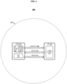
- FIG. 1 illustrates an example of an operating environment 100 that may be representative of various embodiments.
- an evolved node B (eNB) 102 generally serves a cell 103, and may provide user equipment (UE) 104 with wireless connectivity via a wireless carrier of cell 103.
- eNB 102 may identify data 110 to be transmitted to UE 104.
- eNB 102 may schedule transmission of data 110 for an upcoming subframe, which may be referred to as the "transmit subframe" for data 110.
- eNB 102 may send a downlink (DL) scheduling command 106 to UE 104 over a physical downlink control channel (PDCCH) or enhanced physical downlink control channel (EPDCCH), collectively depicted in FIG. 1 as (E)PDCCH 108.
- eNB 102 may then transmit data 110 to UE 104 over a physical downlink shared channel (PDSCH) 112 during the transmit subframe for data 110.
- PDSCH physical downlink shared channel
- UE 104 may identify the transmit subframe of data 110 and access one or more resources of PDSCH 112 during that transmit subframe to receive data 110.
- UE 104 may generate HARQ feedback 114.
- UE 104 may transmit HARQ feedback 114 to eNB 102 over a physical uplink control channel (PUCCH) 116. More particularly, in some embodiments, UE 104 may transmit HARQ feedback 114 to eNB 102 using a particular PUCCH resource of PUCCH 116 and according to a particular PUCCH format.
- PUCCH physical uplink control channel
- UE 104 may be configured to use HARQ feedback 114 to provide feedback for one or more other DL data transmissions in addition to that of data 110. In some embodiments, UE 104 may be configured to use HARQ feedback 114 to provide feedback for one or more DL data transmissions occurring during a different subframe (or set of different subframes) than that during which the DL transmission of data 110 occurs. In various embodiments, UE 104 may be configured to use HARQ feedback 114 to provide feedback for one or more DL data transmissions performed using a different carrier (or set of different carriers) than that used for the DL transmission of data 110.
- UE 104 may be configured to use HARQ feedback 114 to provide feedback for DL data transmissions of multiple subframes and multiple carriers.
- carrier aggregation may be used to enable DL data transmission to UE 104 via each of a set of aggregated component carriers, and UE 104 may be configured to use HARQ feedback 114 to provide feedback for DL transmissions collectively performed during multiple subframes using multiple such component carriers.
- cell 103 may comprise a primary cell (PCell) with respect to wireless communications with/by UE 104. The embodiments are not limited in this context.
- UE 104 may select the PUCCH format that it uses for transmission of HARQ feedback 114 based on the size of HARQ feedback 114, which in turn may depend on the amount of transmitted DL data for which feedback is being provided. For example, in some embodiments, UE 104 may use one of relatively compact PUCCH formats 1a or 1b if HARQ feedback 114 merely includes feedback for DL data transmission of a single subframe and single carrier, and may use the larger PUCCH format 3 if HARQ feedback 114 includes feedback for DL data transmissions of multiple subframes and/or multiple component carriers.
- an enhanced carrier aggregation scheme may be implemented to enable DL data transmission to UE 104 via any or all of a larger number of component carriers than are aggregated according to conventional techniques.
- an enhanced carrier aggregation scheme may be implemented to enable DL data transmission to UE 104 via up to 32 component carriers, rather than limiting such transmissions to a maximum of five component carriers in accordance with conventional LTE carrier aggregation protocols.
- conventional PUCCH formats may not be large enough to accommodate the potential amounts of HARQ feedback that may need to be transmitted at one time.
- PUCCH format 3 may be used to accommodate up to 21 bits of HARQ feedback
- the provision of HARQ feedback for respective DL data transmissions over each of 32 component carriers may require 64 bits if cell 103 is a frequency division duplexing (FDD) cell, and potentially 128 bits or more if cell 103 is a time division duplexing (TDD) cell.
- FDD frequency division duplexing
- TDD time division duplexing
- an enhanced PUCCH format may be implemented.
- an enhanced PUCCH format may be implemented that may be used to transmit up to 128 bits of HARQ feedback.
- significant amounts of PUCCH resources may be wasted.
- an enhanced PUCCH format designed to accommodate a 128-bit HARQ feedback payload is used to transmit 10 bits of HARQ feedback, the majority of the resources consumed by the PUCCH transmission may be wasted.
- the embodiments are not limited to this example.
- an eNB such as eNB 102 may include HARQ feedback configuration information in a DL scheduling command in order to specify one or more HARQ feedback configuration parameters.
- the one or more HARQ feedback configuration parameters may include a PUCCH format to be used for HARQ feedback transmission.
- the one or more HARQ feedback configuration parameters may include a PUCCH resource to be used for HARQ feedback transmission.
- the one or more HARQ feedback configuration parameters may include a HARQ feedback payload size. The embodiments are not limited in this context.
- FIG. 2 illustrates an example of an operating environment 200 that may be representative of the implementation of one or more of the disclosed HARQ feedback configuration techniques according to some embodiments.
- eNB 102 may send a DL scheduling command 206 to UE 104 over (E)PDCCH 108 in order to notify UE 104 of an upcoming transmission of data 210 to UE 104 over PDSCH 112.
- UE 104 may monitor the appropriate resource(s) of PDSCH 112 during the transmit subframe for data 210.
- UE 104 may then include HARQ feedback for data 210 in HARQ feedback 214 that it transmits over PUCCH 116 to eNB 102.
- HARQ feedback 214 may include feedback for one or more other DL data transmissions to UE 104.
- HARQ feedback 214 may include respective feedback for DL data transmissions to UE 104 over each of multiple component carriers.
- PDSCH 112 may comprise a PDSCH of one of a plurality of aggregated component carriers, and HARQ feedback 214 may include feedback for DL data transmissions to UE 104 over respective PDSCHs of one or more other component carriers comprised among the plurality of aggregated component carriers.
- HARQ feedback 214 may include respective feedback for DL data transmissions to UE 104 during each of multiple subframes.
- UE 104 may need to provide HARQ feedback for each of a set of multiple DL subframes, and HARQ feedback 214 may comprise the respective HARQ feedback for each such DL subframe.
- HARQ feedback bundling window shall be employed to denote such a set of multiple DL subframes.
- DL scheduling command 206 may comprise HARQ feedback configuration information (HFCI) field 218.
- HFCI field 218 may comprise a one-bit field.
- HFCI field 218 may only be permitted to be present in DL scheduling commands that map onto UE-specific (E)PDCCH search spaces corresponding to the cell radio network temporary identifiers (C-RNTIs) to which they are addressed.
- eNB 102 may construct DL scheduling command 206 according to a particular defined DL control information (DCI) format. In some embodiments, that DCI format may comprise an enhanced version of a conventional DCI format.
- DCI DL control information
- enhanced versions of one or more of DCI formats 1, 1A, 1B, 1D, 2, 2A, 2B, 2C, and 2D may be defined that include HFCI field 218, and eNB 102 may construct DL scheduling command 206 in accordance with one such enhanced DCI format.
- the embodiments are not limited in this context.
- eNB 102 may use HFCI field 218 to indicate a PUCCH format that UE 104 should use in transmitting HARQ feedback 214 over PUCCH 116 to eNB 102.
- eNB 102 may select the value of HFCI field 218 based on the value-to-parameter correspondences illustrated in Table 1 below.
- eNB 102 may set HFCI field 218 to '0' in order to indicate that UE 104 should use a first PUCCH format in transmitting HARQ feedback 214, or may set HFCI field 218 to '1' in order to indicate that UE 104 should use a second PUCCH format in transmitting HARQ feedback 214.
- the first and second PUCCH formats may include a conventional PUCCH format and an enhanced PUCCH format designed to accommodate larger HARQ feedback payloads.
- eNB 102 may set the value of HFCI field 218 to '1' in order to indicate that such an enhanced PUCCH format is to be used, or may set the value of HFCI field 218 to '0' in order to indicate that PUCCH format 3 is to be used.
- both of the two PUCCH formats may comprised enhanced PUCCH formats. The embodiments are not limited in this context.
- UE 104 may identify a PUCCH format according to which to transmit HARQ feedback 214 over PUCCH 116 to eNB 102. In some embodiments, based on the identified PUCCH format, UE 104 may identify a PUCCH resource to be used in transmitting HARQ feedback 214 over PUCCH 116 to eNB 102. In various embodiments, UE 104 may identify the PUCCH resource as one of four PUCCH resources associated with the PUCCH format according to higher-layer configuration.
- UE 104 may identify the PUCCH resource based on the value of a transmit power control (TPC) field comprised in a DL scheduling command - which may or may not be DL scheduling command 206 - that is associated with a DL data transmission for which HARQ feedback 214 includes feedback and that contains a DL assignment index (DAI) value that is greater than 1.
- TPC transmit power control
- DAI DL assignment index
- UE 104 may determine a HARQ payload size O ACK for HARQ feedback 214 based on the identified PUCCH format.
- particular respective HARQ payload sizes for use in conjunction with the first and second PUCCH formats may be predefined, or may be configured by higher layer signaling.
- O ACK may be predefined or configured by higher layers to be equal to 21 when PUCCH format 3 is being used, and may be predefined or configured by higher layers to be equal to 64 or 128 when an enhanced PUCCH format designed to accommodate larger HARQ feedback payloads is being used. The embodiments are not limited to this example.
- UE 104 may construct HARQ feedback 214 as a sequence of O ACK bits O 0 ACK , O 1 ACK , ... , O O ACK ⁇ 1 ACK .
- UE 104 may order the bits O 0 ACK , O 1 ACK , ... , O O ACK ⁇ 1 ACK according to the values of DAI fields comprised in the DL scheduling commands corresponding to those DL data transmissions.
- the HARQ feedback for a PDSCH transmission with a corresponding PDCCH/EPDCCH transmission or for a PDCCH/EPDCCH indicating downlink semi-persistent scheduling (SPS) release in a subframe n-k may be associated with O DAI k ⁇ 1 ACK if a configured transmission mode supports one transport block or spatial HARQ feedback bundling is applied, and otherwise may be associated with O 2 DAI k ⁇ 2 ACK and O 2 DAI k ⁇ 1 ACK , where DAI ( k ) represents the value of the DAI field in a detected DL scheduling command of DCI format 1, 1A, 1B, 1D, 2, 2A, 2B, 2C, or 2D detected in the HARQ feedback bundling window, and O 2 DAI k ⁇ 2 ACK and O 2 DAI k ⁇ 1 ACK represent HARQ feedback for codewords 0 and 1, respectively.
- HARQ feedback for a PDSCH transmission for which there is no corresponding PDCCH/EPDCCH transmission may be mapped to O O ACK ⁇ 1 ACK .
- HARQ feedback bits that correspond to PDCCH/EPDCCH transmissions without any detected corresponding PDSCH transmissions or correspond to non-detected PDCCH/EPDCCH downlink SPS release indications may be set to NACK. The embodiments are not limited in this context.
- FIG. 3 illustrates an example of a HARQ feedback generation process 300 that may be representative of the implementation of one or more of the disclosed HARQ feedback configuration techniques according to various embodiments.
- HARQ feedback generation process 300 may be representative of a HARQ feedback generation process that UE 104 may use to generate HARQ feedback 214 following a determination that HARQ feedback 214 is to be transmitted using PUCCH format 3 and a determination that HARQ feedback 214 is to comprise 21 bits.
- HARQ feedback generation process 300 for a UE configured with an aggregated set of ten component carriers - each corresponding to a respective one of cells 0 to 9 - a HARQ feedback bit sequence 304 may be generated for a HARQ feedback bundling window 302.
- HARQ feedback bundling window 302 comprises a series of four subframes: subframe n, subframe n+1, subframe n+2, and subframe n+3. The embodiments are not limited to this example.
- construction of HARQ feedback bit sequence 304 proceeds on a subframe-by-subframe basis, and within each subframe, on a cell-by-cell basis. For each subframe, any cells for which previously received DL scheduling commands had indicated scheduled DL data transmissions may be identified, and for each such cell, a respective HARQ feedback bit may be generated to indicate whether the scheduled DL data transmission was successfully received. For example, cells 0, 2, 5, and 8 may be identified as cells from which DL data transmissions were expected during subframe n, and HARQ feedback bits b 0 , b 1 , b 2 , and b 3 may be generated to indicate whether the scheduled DL data transmissions were successfully received from respective cells 0, 2, 5, and 8 during subframe n.
- DAI values comprised in received DL scheduling commands pertaining to HARQ feedback bundling window 302 may be analyzed.
- HARQ feedback generation process 300 when discontinuities are detected in such DAI values, HARQ feedback bits may be generated for DL data transmissions of which the UE had been unaware.
- DL scheduling commands corresponding to DL data transmissions of cells 2 and 3 during subframe n+1 may have been missed.
- HARQ feedback bits b 4 , b 5 , b 6 , and b 7 may be generated for subframe n+1. Bits b 4 and b 7 may be set to indicate whether DL data transmissions were successfully received from respective cells 0 and 8 during subframe n+1, and bits b 5 and b 6 may be set to NACKs.
- HARQ feedback bits b 8 , b 9 , and b 10 may be generated. Bits b 8 and b 10 may be set to indicate whether DL data transmissions were successfully received from respective cells 2 and 6 during subframe n+2, and bit b 9 may be set to a NACK based on detection of a missed DL scheduling command, which in this example was a DL scheduling command for a DL data transmission of cell 4. For subframe n+3, a HARQ feedback bit b 11 may be generated and set to indicate whether a DL data transmission was successfully received from cell 7 during subframe n+3.
- HARQ feedback bit sequence 304 may be generated by concatenating HARQ feedback bits b 0 to b 20 to obtain a bit sequence of 21 bits.
- the embodiments are not limited to this example.
- FIG. 4 illustrates an example of an operating environment 400 that may be representative of some embodiments.
- UE 104 may receive DL scheduling command 206 and generate HARQ feedback 214.
- DL scheduling command 206 may comprise a multi-bit HFCI field 418.
- eNB 102 may use multi-bit HFCI field 418 to specify multiple HARQ feedback configuration parameters
- HFCI field 418 may only be permitted to be present in DL scheduling commands that map onto UE-specific (E)PDCCH search spaces corresponding to the cell radio network temporary identifiers (C-RNTIs) to which they are addressed.
- E UE-specific
- C-RNTIs cell radio network temporary identifiers
- enhanced versions of one or more of DCI formats 1, 1A, 1B, 1D, 2, 2A, 2B, 2C, and 2D may be defined that include multi-bit HFCI field 418, and eNB 102 may construct DL scheduling command 206 in accordance with one such enhanced DCI format.
- the embodiments are not limited in this context.
- Table 2 illustrates a first example of a value-to-parameter mapping that may be defined in some embodiments for a two-bit HFCI field 418.
- eNB 102 may use HFCI field 418 to indicate both a PUCCH format and a PUCCH resource that UE 104 should use in transmitting HARQ feedback 214 over PUCCH 116 to eNB 102.
- eNB 102 may set HFCI field 418 to '00' to indicate a first PUCCH format and a first PUCCH resource, may set HFCI field 418 to '01' to indicate the first PUCCH format and a second PUCCH resource, may set HFCI field 418 to '10' to indicate a second PUCCH format and the first PUCCH resource, or may set HFCI field 418 to '11' to indicate the second PUCCH format and the second PUCCH resource.
- Table 3 illustrates a second example of a value-to-parameter mapping that may be defined in various embodiments for a two-bit HFCI field 418.
- the mapping illustrated in Table 3 may enable eNB 102 to use HFCI field 418 to indicate both a PUCCH format and a PUCCH resource that UE 104 should use in transmitting HARQ feedback 214 over PUCCH 116 to eNB 102.
- the value-to-parameter mapping illustrated in Table 3 may enable eNB 102 to select a PUCCH resource for use with PUCCH format 2 from among three candidate values rather than two.
- eNB 102 may set HFCI field 418 to '00' to indicate a first PUCCH format and a first PUCCH resource, may set HFCI field 418 to '01' to indicate a second PUCCH format and the first PUCCH resource, may set HFCI field 418 to '10' to indicate the second PUCCH format and a second PUCCH resource, or may set HFCI field 418 to '11' to indicate the second PUCCH format and a third PUCCH resource.
- respective corresponding HARQ feedback payload sizes may be predefined or configured by higher-layer signaling for the first and second PUCCH formats in conjunction with the use of a two-bit HFCI field 418 according to the value-to-parameter mapping of Table 2 or Table 3.
- a 21-bit HARQ feedback payload size may be predefined for the first PUCCH format and a 128-bit HARQ feedback payload size may be predefined for the second PUCCH format.
- the first PUCCH format may comprise PUCCH format 3 and the second PUCCH format may comprise an enhanced PUCCH format designed to accommodate larger HARQ feedback payloads.
- the second PUCCH format may comprise a physical uplink shared channel (PUSCH)-based PUCCH format. The embodiments are not limited in this context.
- Table 4 illustrates a third example of a value-to-parameter mapping that may be defined in some embodiments for a two-bit HFCI field 418.
- eNB 102 may use HFCI field 418 to indicate a PUCCH format and either a PUCCH resource or a HARQ feedback payload size.
- eNB 102 may set HFCI field 418 to '00' to indicate a first PUCCH format and a first PUCCH resource, may set HFCI field 418 to '01' to indicate the first PUCCH format and a second PUCCH resource, may set HFCI field 418 to '10' to indicate a second PUCCH format and a first HARQ feedback payload size, and may set HFCI field 418 to '11' to indicate the second PUCCH format and a second HARQ feedback payload size.
- the first PUCCH format corresponding to respective HFCI field 418 values of '00' and '01' according to the value-to-parameter mapping of Table 4 may comprise PUCCH format 3.
- the second PUCCH format corresponding to respective HFCI field 418 values of '10' and '11' according to the value-to-parameter mapping of Table 4 may comprise an enhanced PUCCH format designed to accommodate larger HARQ feedback payloads.
- the first and second HARQ feedback payload sizes corresponding to respective HFCI field 418 values of '10' and '11' according to the value-to-parameter mapping of Table 4 may both be comprised among a set of HARQ feedback payload sizes designated for use in conjunction with the enhanced PUCCH format.
- the first and second HARQ feedback payload size may comprise two different numbers of bits comprised among the set ⁇ 32 bits, 64 bits, 128 bits ⁇ .
- HARQ feedback payload sizes to which HFCI field 418 values of '10' and '11' may be used to refer may be defined to differ between TDD environments and FDD environments.
- HFCI field 418 values of '10' and '11' may indicate 64-bit and 128-bit HARQ feedback payload sizes, respectively.
- HFCI field 418 values of '10' and '11' may indicate 32-bit and 64-bit HARQ feedback payload sizes, respectively. The embodiments are not limited to this example.
- Table 5 illustrates a fourth example of a value-to-parameter mapping that may be defined in some embodiments for a two-bit HFCI field 418.
- the mapping illustrated in Table 5 may enable eNB 102 to use HFCI field 418 to indicate a PUCCH format and either a PUCCH resource or a HARQ feedback payload size.
- the value-to-parameter mapping illustrated in Table 5 may enable eNB 102 to select a HARQ feedback payload size for use with PUCCH format 2 from among three candidate sizes rather than two.
- eNB 102 may set HFCI field 418 to '00' to indicate a first PUCCH format and a first PUCCH resource, may set HFCI field 418 to '01' to indicate a second PUCCH format and a first HARQ feedback payload size, may set HFCI field 418 to '10' to indicate the second PUCCH format and a second HARQ feedback payload size, and may set HFCI field 418 to '11' to indicate the second PUCCH format and a third HARQ feedback payload size.
- a particular HARQ feedback payload size to be used in combination with the first PUCCH format may be predefined or configured by higher-layer signaling.
- a HARQ feedback payload size of 21 bits may be predefined or configured by higher-layer signaling for use with the first PUCCH format, which may comprise PUCCH format 3.
- a particular PUCCH resource to be used in combination with the second PUCCH format may be predefined or configured by higher-layer signaling. The embodiments are not limited in this context.
- Table 6 illustrates a fifth example of a value-to-parameter mapping that may be defined in some embodiments for a two-bit HFCI field 418.
- eNB 102 may use HFCI field 418 to indicate a PUCCH format and one or both of a PUCCH resource and a HARQ feedback payload size.
- eNB 102 may set HFCI field 418 to '00' to indicate a first PUCCH format and a first PUCCH resource, may set HFCI field 418 to '01' to indicate a second PUCCH format, the first PUCCH resource, and a first HARQ feedback payload size, may set HFCI field 418 to '10' to indicate the second PUCCH format, a second PUCCH resource, and the first HARQ feedback payload size, or may set HFCI field 418 to '11' to indicate the second PUCCH format and a second HARQ feedback payload size.
- a particular HARQ feedback payload size to be used in combination with the first PUCCH format and the first PUCCH resource may be predefined or configured by higher-layer signaling.
- a particular PUCCH resource to be used in combination with the second PUCCH format and the second HARQ feedback payload size may be predefined or configured by higher-layer signaling. The embodiments are not limited in this context.
- Table 7 illustrates a sixth example of a value-to-parameter mapping that may be defined in various embodiments for a two-bit HFCI field 418.
- eNB 102 may use HFCI field 418 to indicate a PUCCH format and a PUCCH resource, and possibly a HARQ feedback payload size as well.
- eNB 102 may set HFCI field 418 to '00' to indicate a first PUCCH format and a first PUCCH resource, may set HFCI field 418 to '01' to indicate a second PUCCH format, the first PUCCH resource, and a first HARQ feedback payload size, may set HFCI field 418 to '10' to indicate the second PUCCH format, a second PUCCH resource, and a second HARQ feedback payload size, or may set HFCI field 418 to '11' to indicate the second PUCCH format, a third PUCCH resource, and a third HARQ feedback payload size.
- a particular HARQ feedback payload size to be used in combination with the first PUCCH format and the first PUCCH resource may be predefined or configured by higher-layer signaling. The embodiments are not limited in this context.
- Tables 2 to 7 illustrate various examples of value-to-parameter mappings that may be defined for an HFCI field 418 comprising two bits
- an HFCI field 418 comprising more than two bits may be implemented in various embodiments.
- Table 8 illustrates an example of a value-to-parameter mapping that may be defined in some embodiments for an X-bit HFCI field 418, where X > 2.
- Table 8 Decimal Value of Bit String in X-Bit HFCI Field 418 W 0 1 1 2 2 3 ... ... 2 X -1 2 X
- eNB 102 may use an X-bit HFCI field 418 to indicate a value of a parameter W. More particularly, in this example, eNB 102 may use the X -bit HFCI field 418 to identify an integer in the inclusive range [1, 2 X ] as the value of W. In various embodiments, following receipt of DL scheduling command 206, UE 104 may identify the value of W based on the contents of HFCI field 418 and may then identify - based on the value of W - a HARQ feedback payload size to be used in transmitting HARQ feedback 214 over PUCCH 116 to eNB 102.
- O ACK W + 2 X U ⁇ W / 2 X
- U denotes a total number of PDSCH transmissions and PDCCH downlink SPS release indications received during a HARQ feedback bundling window.
- UE 104 may determine one or both of a PUCCH format and a PUCCH resource for use in transmitting HARQ feedback 214 over PUCCH 116 to eNB 102.
- UE 104 may transmit HARQ feedback 214 using a first PUCCH format and a corresponding first PUCCH resource if O ACK ⁇ 21, and may transmit HARQ feedback 214 using a second PUCCH format and a corresponding second PUCCH resource if O ACK > 21.
- the first PUCCH format may comprise PUCCH format 3
- the second PUCCH format may comprise an enhanced PUCCH format designed to accommodate larger HARQ feedback payloads. The embodiments are not limited in this context.
- Table 9 illustrates a more generalized form of a value-to-parameter mapping that may be defined in some embodiments for X -bit HFCI field 418.
- each of 2 X -1 possible values of d - where d represents a decimal value of a bit string of X bits contained in HFCI field 418 - is defined to indicate a particular respective set of HARQ feedback configuration parameters ⁇ F d , O ACK d , R d ⁇ .
- F d may comprise a PUCCH format indicated by that value of d
- O ACK d may comprise a HARQ feedback payload size indicated by that value of d
- R d may comprise a PUCCH resource indicated by that value of d.
- Table 9 Decimal Value d of Bit String in X-Bit HFCI Field 418 PUCCH Format HARQ Feedback Payload Size PUCCH Resource 0 F 0 O ACK 0 R 0 1 F 1 O ACK 1 R 1 ... ... ... ... 2 X -1 F 2 X -1 O ACK X ⁇ 1 2 R 2 X -1
- Table 10 illustrates an example of such an embodiment.
- HFCI field 418 comprises 3 bits, and thus X is equal to three.
- F 0 and F 1 both correspond to PUCCH format 3, while F 2 to F 7 all correspond to an enhanced PUCCH format designed to accommodate larger HARQ feedback payloads.
- O ACK 0 and O ACK 1 both correspond to a 21-bit HARQ feedback payload size
- O ACK 2 , O ACK 3 , and O ACK 4 each correspond to a 64-bit HARQ feedback payload size
- O ACK 5 , O ACK 6 , and O ACK 7 each correspond to a 128-bit HARQ feedback payload size
- R 0 , R 2 , and R 5 each correspond to a first PUCCH resource
- R 1 , R 3 , and R 6 each correspond to a second PUCCH resource
- R 4 and R 7 both correspond to a third PUCCH resource.
- a conventional field within DL scheduling command 206 may be repurposed for use as HFCI field 418.
- a 2-bit TPC field in DL scheduling command 206 may be used as a 2-bit HFCI field 418.
- such repurposing of TPC fields as 2-bit HFCI fields may be limited to TPC fields comprised in PDCCH assignments with DAI values greater than '1' or DAI values equal to '1' that are not the first PDCCH transmissions on the primary cell and TPC fields comprised in DCI of the corresponding PDCCH detected on the secondary cell. The embodiments are not limited in this context.
- a conventional field within DL scheduling command 206 may be repurposed for use in combination with HFCI field 418 in conjunction with the indication of one or more HARQ feedback configuration parameters.
- the collective set of bits comprised in HFCI field 418 and a TPC field may indicate one or more of a PUCCH format, a PUCCH resource, and a HARQ feedback payload size.
- the repurposed field may be used to independently specify one or more HARQ feedback configuration parameters.
- the TPC field may be used to indicate a PUCCH format
- HFCI field 418 may be used to indicate a PUCCH resource and a HARQ feedback payload size.
- HFCI field 418 and the repurposed field may be used to provide bits to be combined to obtain a bit string that maps to a particular set of HARQ feedback configuration parameters.
- UE 104 may obtain a bit string by concatenation the bits in HFCI field 418 with the bits in the TPC field, and may determine a set of HARQ feedback configuration parameters according to a value-to-parameter mapping of the general form illustrated in Table 9. The embodiments are not limited in this context.
- UE 104 may generate HARQ feedback 214 according to a HARQ feedback generation process that implements a cell-group-based approach to HARQ feedback payload size adaptation.
- the various configured DL component carriers may be divided into multiple HARQ feedback cell groups (CGs).
- the number of CGs may be an integer power of 2 and/or each CG may comprise a same number of component carriers.
- each CG may be assigned a unique CG identifier (ID).
- HFCI field 418 may comprise a bitmap that includes, for each of the multiple CGs, a respective bit that indicates whether a PDSCH transmission or SPS release is scheduled on at least one DL component carrier of that CG during the HARQ feedback bundling window.
- UE 104 may determine a HARQ feedback payload size based on such a bitmap comprised in HFCI field 418.
- UE 104 may generate a pre-defined number of HARQ feedback bits. In some embodiments, if the component carriers correspond to FDD cells, UE 104 may a number of HARQ feedback bits equal to the number of component carriers comprised in the CG. In various embodiments, if the component carriers correspond to TDD cells, UE 104 may generate a number of HARQ feedback bits equal to the total number of subframes comprised within the HARQ feedback bundling window. In some embodiments, UE 104 may refrain from generating HARQ feedback bits for any CG with respect to which neither a PDSCH transmission nor an SPS release is scheduled on any component carrier during the HARQ feedback bundling window.
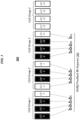
- FIG. 5 illustrates an example of a HARQ feedback generation process 500 that may be representative of a CG-based HARQ feedback generation process.
- UE 104 may perform the HARQ feedback generation process illustrated in FIG. 5 in response to receipt of a DL scheduling command 206 in which HFCI field 418 contains the bitmap '1110'.
- UE 104 may determine that HARQ feedback bits are to be generated for CGs 1, 2, and 3, but not for CG 4.
- Each of CGs 1, 2, 3, and 4 comprises four respective component carriers.
- these various component carriers may correspond to FDD cells, and thus UE 104 may generate four respective HARQ feedback bits for each of CGs 1, 2, and 3, and assemble those various HARQ feedback bits into a 12-bit HARQ feedback bit sequence 504.
- UE 104 may select a PUCCH format for use in transmission of HARQ feedback 214 based on the size of HARQ feedback bit sequence 504.
- the HARQ feedback payload can be further compressed according to the value of the DAI field with respect to each CG for which HARQ feedback bits are generated. The embodiments are not limited in this context.
- UE 104 may be configured to autonomously select and use PUCCH format 1a/1b and a corresponding PUCCH resource to transmit HARQ feedback 214 under certain circumstances.
- UE 104 may be configured to autonomously select and use PUCCH format 1a/1b and a corresponding PUCCH resource when received DCI indicates only a PDSCH transmission or SPS release in the primary cell during the HARQ-ACK bundling window.
- the corresponding PUCCH resource may be determined according to the lowest control channel element (CCE) index used to construct the PDCCH.
- CCE control channel element
- UE 104 may be configured to autonomously select and use PUCCH format 1a/1b and a corresponding PUCCH resource to transmit HARQ feedback for a primary cell PDSCH transmission during a subframe of the HARQ feedback bundling window for which no corresponding PDCCH/EPDCCH transmission is detected within that subframe.
- UE 104 may select the corresponding PUCCH resource from among four PUCCH resource values configured by higher layers, based on the value comprised in a TPC command for PUCCH field in DCI used to indicate a semi-persistent DL scheduling activation.
- the embodiments are not limited in this context.
- FIG. 1 Some of the figures may include a logic flow. Although such figures presented herein may include a particular logic flow, it can be appreciated that the logic flow merely provides an example of how the general functionality as described herein can be implemented. Further, the given logic flow does not necessarily have to be executed in the order presented unless otherwise indicated. In addition, the given logic flow may be implemented by a hardware element, a software element executed by a processor, or any combination thereof. The embodiments are not limited in this context.
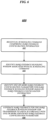
- FIG. 6 illustrates an example of a logic flow 600 that may be representative of the implementation of one or more of the disclosed HARQ feedback configuration techniques according to various embodiments.
- logic flow 600 may be representative of operations that may be performed in some embodiments by UE 104 in operating environment 200 of FIG. 2 or operating environment 400 of FIG. 4 .
- a DL scheduling command may be received at 602 that comprises HARQ feedback configuration information.
- UE 104 may receive a DL scheduling command 206 from eNB 102, and the DL scheduling command 206 may comprise an HFCI field 218 or HFCI field 418 containing HARQ feedback configuration information.
- a HARQ feedback bundling window associated with the DL scheduling command may be identified.
- UE 104 may identify a HARQ feedback bundling window associated with DL scheduling command 206.
- HARQ feedback 214 may comprise HARQ feedback for a HARQ feedback bundling window
- UE 104 may identify one or more of a PUCCH format to be used for transmission of HARQ feedback 214, a PUCCH resource for use in transmission of HARQ feedback 214, and a HARQ feedback payload size for HARQ feedback 214 based on HARQ feedback configuration information comprised in HFCI field 218 or HFCI field 418.
- HARQ feedback for the HARQ feedback bundling window may be generated for transmission to an eNB in accordance with the one or more identified HARQ feedback configuration parameters.
- UE 104 may generate HARQ feedback 214 for transmission to eNB 102 in accordance with the one or more HARQ feedback configuration parameters identified at 606.
- the embodiments are not limited to these examples.
- FIG. 7 illustrates an example of a logic flow 700 that may be representative of the implementation of one or more of the disclosed HARQ feedback configuration techniques according to various embodiments.
- logic flow 700 may be representative of operations that may be performed in some embodiments by eNB 102 in operating environment 200 of FIG. 2 or operating environment 400 of FIG. 4 .
- a HARQ feedback bundling window for which HARQ feedback is to be received from a UE may be identified at 702.
- eNB 102 may identify a HARQ feedback bundling window for which it is to receive HARQ feedback 214 from UE 104.
- one or more HARQ feedback configuration parameters for the HARQ feedback may be determined.
- eNB 102 may determine one or more of a PUCCH format to be used by UE 104 for transmission of HARQ feedback 214, a PUCCH resource to be used by UE 104 in transmission of HARQ feedback 214, and a HARQ feedback payload size to be used by UE 104 for HARQ feedback 214.
- a DL data transmission to the UE that is scheduled for a subframe in the HARQ feedback bundling window may be identified.
- eNB 102 may identify a DL transmission of data 210 to UE 104 that is scheduled for a subframe comprised in the HARQ feedback bundling window.
- downlink control information may be generated for transmission to the UE to indicate the scheduling of the DL data transmission, and the downlink control information may comprise HARQ feedback configuration information to indicate at least one of the one or more HARQ feedback configuration parameters determined at 704.
- eNB 102 may generate a DL scheduling command 206 for transmission to UE 104 to indicate the scheduling of the DL transmission of data 210 to UE 104 during the subframe comprised in the HARQ feedback bundling window
- DL scheduling command 206 may comprise an HFCI field 218 or HFCI field 418 containing HARQ feedback configuration information that indicates one or more of a PUCCH format to be used by UE 104 for transmission of HARQ feedback 214, a PUCCH resource to be used by UE 104 in transmission of HARQ feedback 214, and a HARQ feedback payload size to be used by UE 104 for HARQ feedback 214.
- the embodiments are not limited to these examples.
- FIG. 8 illustrates an embodiment of a storage medium 800 and an embodiment of a storage medium 850.
- Storage media 800 and 850 may comprise any non-transitory computer-readable storage media or machine-readable storage media, such as an optical, magnetic or semiconductor storage media.
- storage media 800 and 850 may comprise an article of manufacture.
- storage media 800 and 850 may store computer-executable instructions, such as computer-executable instructions to implement logic flow 600 of FIG. 6 and logic flow 700 of FIG. 7 , respectively.
- Examples of a computer-readable storage medium or machine-readable storage medium may include any tangible media capable of storing electronic data, including volatile memory or non-volatile memory, removable or non-removable memory, erasable or non-erasable memory, writeable or re-writeable memory, and so forth.
- Examples of computer-executable instructions may include any suitable type of code, such as source code, compiled code, interpreted code, executable code, static code, dynamic code, object-oriented code, visual code, and the like. The embodiments are not limited in this context.
- circuitry may refer to, be part of, or include an Application Specific Integrated Circuit (ASIC), an electronic circuit, a processor (shared, dedicated, or group), and/or memory (shared, dedicated, or group) that execute one or more software or firmware programs, a combinational logic circuit, and/or other suitable hardware components that provide the described functionality.
- ASIC Application Specific Integrated Circuit
- the circuitry may be implemented in, or functions associated with the circuitry may be implemented by, one or more software or firmware modules.
- circuitry may include logic, at least partially operable in hardware. Embodiments described herein may be implemented into a system using any suitably configured hardware and/or software.
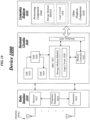
- FIG. 9 illustrates an example of a UE device 900 that may be representative of a UE that implements one or more of the disclosed techniques in various embodiments.
- UE device 900 may be representative of UE 104 according to some embodiments.
- the UE device 900 may include application circuitry 902, baseband circuitry 904, Radio Frequency (RF) circuitry 906, front-end module (FEM) circuitry 908 and one or more antennas 910, coupled together at least as shown.
- RF Radio Frequency
- FEM front-end module
- the application circuitry 902 may include one or more application processors.
- the application circuitry 902 may include circuitry such as, but not limited to, one or more single-core or multi-core processors.
- the processor(s) may include any combination of general-purpose processors and dedicated processors (e.g., graphics processors, application processors, etc.).
- the processors may be coupled with and/or may include memory/storage and may be configured to execute instructions stored in the memory/storage to enable various applications and/or operating systems to run on the system.
- the baseband circuitry 904 may include circuitry such as, but not limited to, one or more single-core or multi-core processors.
- the baseband circuitry 904 may include one or more baseband processors and/or control logic to process baseband signals received from a receive signal path of the RF circuitry 906 and to generate baseband signals for a transmit signal path of the RF circuitry 906.
- Baseband processing circuity 904 may interface with the application circuitry 902 for generation and processing of the baseband signals and for controlling operations of the RF circuitry 906.
- the baseband circuitry 904 may include a second generation (2G) baseband processor 904a, third generation (3G) baseband processor 904b, fourth generation (4G) baseband processor 904c, and/or other baseband processor(s) 904d for other existing generations, generations in development or to be developed in the future (e.g., fifth generation (5G), 6G, etc.).
- the baseband circuitry 904 e.g., one or more of baseband processors 904a-d
- the radio control functions may include, but are not limited to, signal modulation/demodulation, encoding/decoding, radio frequency shifting, etc.
- modulation/demodulation circuitry of the baseband circuitry 904 may include Fast-Fourier Transform (FFT), precoding, and/or constellation mapping/demapping functionality.
- FFT Fast-Fourier Transform
- encoding/decoding circuitry of the baseband circuitry 904 may include convolution, tail-biting convolution, turbo, Viterbi, and/or Low Density Parity Check (LDPC) encoder/decoder functionality.
- LDPC Low Density Parity Check
- the baseband circuitry 904 may include elements of a protocol stack such as, for example, elements of an evolved universal terrestrial radio access network (EUTRAN) protocol including, for example, physical (PHY), media access control (MAC), radio link control (RLC), packet data convergence protocol (PDCP), and/or radio resource control (RRC) elements.
- EUTRAN evolved universal terrestrial radio access network
- a central processing unit (CPU) 904e of the baseband circuitry 904 may be configured to run elements of the protocol stack for signaling of the PHY, MAC, RLC, PDCP and/or RRC layers.
- the baseband circuitry may include one or more audio digital signal processor(s) (DSP) 904f.
- DSP audio digital signal processor
- the audio DSP(s) 904f may be include elements for compression/decompression and echo cancellation and may include other suitable processing elements in other embodiments.
- Components of the baseband circuitry may be suitably combined in a single chip, a single chipset, or disposed on a same circuit board in some embodiments.
- some or all of the constituent components of the baseband circuitry 904 and the application circuitry 902 may be implemented together such as, for example, on a system on a chip (SOC).
- SOC system on a chip
- the baseband circuitry 904 may provide for communication compatible with one or more radio technologies.
- the baseband circuitry 904 may support communication with an evolved universal terrestrial radio access network (EUTRAN) and/or other wireless metropolitan area networks (WMAN), a wireless local area network (WLAN), a wireless personal area network (WPAN).
- EUTRAN evolved universal terrestrial radio access network
- WMAN wireless metropolitan area networks
- WLAN wireless local area network
- WPAN wireless personal area network
- multi-mode baseband circuitry Embodiments in which the baseband circuitry 904 is configured to support radio communications of more than one wireless protocol.
- RF circuitry 906 may enable communication with wireless networks using modulated electromagnetic radiation through a non-solid medium.
- the RF circuitry 906 may include switches, filters, amplifiers, etc. to facilitate the communication with the wireless network.
- RF circuitry 906 may include a receive signal path which may include circuitry to down-convert RF signals received from the FEM circuitry 908 and provide baseband signals to the baseband circuitry 904.
- RF circuitry 906 may also include a transmit signal path which may include circuitry to up-convert baseband signals provided by the baseband circuitry 904 and provide RF output signals to the FEM circuitry 908 for transmission.
- the RF circuitry 906 may include a receive signal path and a transmit signal path.
- the receive signal path of the RF circuitry 906 may include mixer circuitry 906a, amplifier circuitry 906b and filter circuitry 906c.
- the transmit signal path of the RF circuitry 906 may include filter circuitry 906c and mixer circuitry 906a.
- RF circuitry 906 may also include synthesizer circuitry 906d for synthesizing a frequency for use by the mixer circuitry 906a of the receive signal path and the transmit signal path.
- the mixer circuitry 906a of the receive signal path may be configured to down-convert RF signals received from the FEM circuitry 908 based on the synthesized frequency provided by synthesizer circuitry 906d.
- the amplifier circuitry 906b may be configured to amplify the down-converted signals and the filter circuitry 906c may be a low-pass filter (LPF) or band-pass filter (BPF) configured to remove unwanted signals from the down-converted signals to generate output baseband signals.
- LPF low-pass filter
- BPF band-pass filter
- Output baseband signals may be provided to the baseband circuitry 904 for further processing.
- the output baseband signals may be zero-frequency baseband signals, although this is not a requirement.
- mixer circuitry 906a of the receive signal path may comprise passive mixers, although the scope of the embodiments is not limited in this respect.
- the mixer circuitry 906a of the transmit signal path may be configured to up-convert input baseband signals based on the synthesized frequency provided by the synthesizer circuitry 906d to generate RF output signals for the FEM circuitry 908.
- the baseband signals may be provided by the baseband circuitry 904 and may be filtered by filter circuitry 906c.
- the filter circuitry 906c may include a low-pass filter (LPF), although the scope of the embodiments is not limited in this respect.
- the mixer circuitry 906a of the receive signal path and the mixer circuitry 906a of the transmit signal path may include two or more mixers and may be arranged for quadrature downconversion and/or upconversion respectively.
- the mixer circuitry 906a of the receive signal path and the mixer circuitry 906a of the transmit signal path may include two or more mixers and may be arranged for image rejection (e.g., Hartley image rejection).
- the mixer circuitry 906a of the receive signal path and the mixer circuitry 906a may be arranged for direct downconversion and/or direct upconversion, respectively.
- the mixer circuitry 906a of the receive signal path and the mixer circuitry 906a of the transmit signal path may be configured for super-heterodyne operation.
- the output baseband signals and the input baseband signals may be analog baseband signals, although the scope of the embodiments is not limited in this respect.
- the output baseband signals and the input baseband signals may be digital baseband signals.
- the RF circuitry 906 may include analog-to-digital converter (ADC) and digital-to-analog converter (DAC) circuitry and the baseband circuitry 904 may include a digital baseband interface to communicate with the RF circuitry 906.
- ADC analog-to-digital converter
- DAC digital-to-analog converter
- a separate radio IC circuitry may be provided for processing signals for each spectrum, although the scope of the embodiments is not limited in this respect.
- the synthesizer circuitry 906d may be a fractional-N synthesizer or a fractional N/N+1 synthesizer, although the scope of the embodiments is not limited in this respect as other types of frequency synthesizers may be suitable.
- synthesizer circuitry 906d may be a delta-sigma synthesizer, a frequency multiplier, or a synthesizer comprising a phase-locked loop with a frequency divider.
- the synthesizer circuitry 906d may be configured to synthesize an output frequency for use by the mixer circuitry 906a of the RF circuitry 906 based on a frequency input and a divider control input. In some embodiments, the synthesizer circuitry 906d may be a fractional N/N+1 synthesizer.
- frequency input may be provided by a voltage controlled oscillator (VCO), although that is not a requirement.
- VCO voltage controlled oscillator
- Divider control input may be provided by either the baseband circuitry 904 or the applications processor 902 depending on the desired output frequency.
- a divider control input (e.g., N) may be determined from a look-up table based on a channel indicated by the applications processor 902.
- Synthesizer circuitry 906d of the RF circuitry 906 may include a divider, a delay-locked loop (DLL), a multiplexer and a phase accumulator.
- the divider may be a dual modulus divider (DMD) and the phase accumulator may be a digital phase accumulator (DPA).
- the DMD may be configured to divide the input signal by either N or N+1 (e.g., based on a carry out) to provide a fractional division ratio.
- the DLL may include a set of cascaded, tunable, delay elements, a phase detector, a charge pump and a D-type flip-flop.
- the delay elements may be configured to break a VCO period up into Nd equal packets of phase, where Nd is the number of delay elements in the delay line.
- Nd is the number of delay elements in the delay line.
- synthesizer circuitry 906d may be configured to generate a carrier frequency as the output frequency, while in other embodiments, the output frequency may be a multiple of the carrier frequency (e.g., twice the carrier frequency, four times the carrier frequency) and used in conjunction with quadrature generator and divider circuitry to generate multiple signals at the carrier frequency with multiple different phases with respect to each other.
- the output frequency may be a LO frequency (fLO).
- the RF circuitry 906 may include an IQ/polar converter.
- FEM circuitry 908 may include a receive signal path which may include circuitry configured to operate on RF signals received from one or more antennas 910, amplify the received signals and provide the amplified versions of the received signals to the RF circuitry 906 for further processing.
- FEM circuitry 908 may also include a transmit signal path which may include circuitry configured to amplify signals for transmission provided by the RF circuitry 906 for transmission by one or more of the one or more antennas 910.
- the FEM circuitry 908 may include a TX/RX switch to switch between transmit mode and receive mode operation.
- the FEM circuitry may include a receive signal path and a transmit signal path.
- the receive signal path of the FEM circuitry may include a low-noise amplifier (LNA) to amplify received RF signals and provide the amplified received RF signals as an output (e.g., to the RF circuitry 906).
- the transmit signal path of the FEM circuitry 908 may include a power amplifier (PA) to amplify input RF signals (e.g., provided by RF circuitry 906), and one or more filters to generate RF signals for subsequent transmission (e.g., by one or more of the one or more antennas 910.
- PA power amplifier
- the UE device 900 may include additional elements such as, for example, memory/storage, display, camera, sensor, and/or input/output (I/O) interface.
- additional elements such as, for example, memory/storage, display, camera, sensor, and/or input/output (I/O) interface.
- FIG. 10 illustrates an embodiment of a communications device 1000 that may implement one or more of eNB 102, UE 104, logic flow 600, logic flow 700, storage medium 800, storage medium 850, and UE 900.
- device 1000 may comprise a logic circuit 1028.
- the logic circuit 1028 may include physical circuits to perform operations described for one or more of eNB 102, UE 104, logic flow 600, logic flow 700, and UE 900 of FIG. 9 for example.
- device 1000 may include a radio interface 1010, baseband circuitry 1020, and computing platform 1030, although the embodiments are not limited to this configuration.
- the device 1000 may implement some or all of the structure and/or operations for one or more of eNB 102, UE 104, logic flow 600, logic flow 700, storage medium 800, storage medium 850, UE 900, and logic circuit 1028 in a single computing entity, such as entirely within a single device.
- the device 1000 may distribute portions of the structure and/or operations for one or more of eNB 102, UE 104, logic flow 600, logic flow 700, storage medium 800, storage medium 850, UE 900, and logic circuit 1028 across multiple computing entities using a distributed system architecture, such as a client-server architecture, a 3-tier architecture, an N-tier architecture, a tightly-coupled or clustered architecture, a peer-to-peer architecture, a master-slave architecture, a shared database architecture, and other types of distributed systems.
- a distributed system architecture such as a client-server architecture, a 3-tier architecture, an N-tier architecture, a tightly-coupled or clustered architecture, a peer-to-peer architecture, a master-slave architecture, a shared database architecture, and other types of distributed systems.
- a distributed system architecture such as a client-server architecture, a 3-tier architecture, an N-tier architecture, a tightly-coupled or clustered architecture, a peer-to-peer architecture, a
- radio interface 1010 may include a component or combination of components adapted for transmitting and/or receiving single-carrier or multi-carrier modulated signals (e.g., including complementary code keying (CCK), orthogonal frequency division multiplexing (OFDM), and/or single-carrier frequency division multiple access (SC-FDMA) symbols) although the embodiments are not limited to any specific over-the-air interface or modulation scheme.
- Radio interface 1010 may include, for example, a receiver 1012, a frequency synthesizer 1014, and/or a transmitter 1016.
- Radio interface 1010 may include bias controls, a crystal oscillator and/or one or more antennas 1018- f .
- radio interface 1010 may use external voltage-controlled oscillators (VCOs), surface acoustic wave filters, intermediate frequency (IF) filters and/or RF filters, as desired. Due to the variety of potential RF interface designs an expansive description thereof is omitted.
- VCOs voltage-controlled oscillators
- IF intermediate frequency
- Baseband circuitry 1020 may communicate with radio interface 1010 to process receive and/or transmit signals and may include, for example, a mixer for down-converting received RF signals, an analog-to-digital converter 1022 for converting analog signals to digital form, a digital-to-analog converter 1024 for converting digital signals to analog form, and a mixer for up-converting signals for transmission. Further, baseband circuitry 1020 may include a baseband or physical layer (PHY) processing circuit 1026 for PHY link layer processing of respective receive/transmit signals. Baseband circuitry 1020 may include, for example, a medium access control (MAC) processing circuit 1027 for MAC/data link layer processing. Baseband circuitry 1020 may include a memory controller 1032 for communicating with MAC processing circuit 1027 and/or a computing platform 1030, for example, via one or more interfaces 1034.
- PHY physical layer
- PHY processing circuit 1026 may include a frame construction and/or detection module, in combination with additional circuitry such as a buffer memory, to construct and/or deconstruct communication frames.
- MAC processing circuit 1027 may share processing for certain of these functions or perform these processes independent of PHY processing circuit 1026.
- MAC and PHY processing may be integrated into a single circuit.
- the computing platform 1030 may provide computing functionality for the device 1000. As shown, the computing platform 1030 may include a processing component 1040. In addition to, or alternatively of, the baseband circuitry 1020, the device 1000 may execute processing operations or logic for one or more of eNB 102, UE 104, logic flow 600, logic flow 700, storage medium 800, storage medium 850, UE 900, and logic circuit 1028 using the processing component 1040.
- the processing component 1040 (and/or PHY 1026 and/or MAC 1027) may comprise various hardware elements, software elements, or a combination of both.
- Examples of hardware elements may include devices, logic devices, components, processors, microprocessors, circuits, processor circuits, circuit elements (e.g., transistors, resistors, capacitors, inductors, and so forth), integrated circuits, application specific integrated circuits (ASIC), programmable logic devices (PLD), digital signal processors (DSP), field programmable gate array (FPGA), memory units, logic gates, registers, semiconductor device, chips, microchips, chip sets, and so forth.
- ASIC application specific integrated circuits
- PLD programmable logic devices
- DSP digital signal processors
- FPGA field programmable gate array
- Examples of software elements may include software components, programs, applications, computer programs, application programs, system programs, software development programs, machine programs, operating system software, middleware, firmware, software modules, routines, subroutines, functions, methods, procedures, software interfaces, application program interfaces (API), instruction sets, computing code, computer code, code segments, computer code segments, words, values, symbols, or any combination thereof. Determining whether an embodiment is implemented using hardware elements and/or software elements may vary in accordance with any number of factors, such as desired computational rate, power levels, heat tolerances, processing cycle budget, input data rates, output data rates, memory resources, data bus speeds and other design or performance constraints, as desired for a given implementation.
- the computing platform 1030 may further include other platform components 1050.
- Other platform components 1050 include common computing elements, such as one or more processors, multi-core processors, co-processors, memory units, chipsets, controllers, peripherals, interfaces, oscillators, timing devices, video cards, audio cards, multimedia input/output (I/O) components (e.g., digital displays), power supplies, and so forth.
- Examples of memory units may include without limitation various types of computer readable and machine readable storage media in the form of one or more higher speed memory units, such as read-only memory (ROM), random-access memory (RAM), dynamic RAM (DRAM), Double-Data-Rate DRAM (DDRAM), synchronous DRAM (SDRAM), static RAM (SRAM), programmable ROM (PROM), erasable programmable ROM (EPROM), electrically erasable programmable ROM (EEPROM), flash memory, polymer memory such as ferroelectric polymer memory, ovonic memory, phase change or ferroelectric memory, silicon-oxide-nitride-oxide-silicon (SONOS) memory, magnetic or optical cards, an array of devices such as Redundant Array of Independent Disks (RAID) drives, solid state memory devices (e.g., USB memory, solid state drives (SSD) and any other type of storage media suitable for storing information.
- ROM read-only memory
- RAM random-access memory
- DRAM dynamic RAM
- DDRAM Double
- Device 1000 may be, for example, an ultra-mobile device, a mobile device, a fixed device, a machine-to-machine (M2M) device, a personal digital assistant (PDA), a mobile computing device, a smart phone, a telephone, a digital telephone, a cellular telephone, user equipment, eBook readers, a handset, a one-way pager, a two-way pager, a messaging device, a computer, a personal computer (PC), a desktop computer, a laptop computer, a notebook computer, a netbook computer, a handheld computer, a tablet computer, a server, a server array or server farm, a web server, a network server, an Internet server, a work station, a mini-computer, a main frame computer, a supercomputer, a network appliance, a web appliance, a distributed computing system, multiprocessor systems, processor-based systems, consumer electronics, programmable consumer electronics, game devices, display, television, digital television, set top box, wireless access point, base station, node B
- Embodiments of device 1000 may be implemented using single input single output (SISO) architectures. However, certain implementations may include multiple antennas (e.g., antennas 1018- f ) for transmission and/or reception using adaptive antenna techniques for beamforming or spatial division multiple access (SDMA) and/or using MIMO communication techniques.
- SISO single input single output
- certain implementations may include multiple antennas (e.g., antennas 1018- f ) for transmission and/or reception using adaptive antenna techniques for beamforming or spatial division multiple access (SDMA) and/or using MIMO communication techniques.
- SDMA spatial division multiple access
- device 1000 may be implemented using any combination of discrete circuitry, application specific integrated circuits (ASICs), logic gates and/or single chip architectures. Further, the features of device 1000 may be implemented using microcontrollers, programmable logic arrays and/or microprocessors or any combination of the foregoing where suitably appropriate. It is noted that hardware, firmware and/or software elements may be collectively or individually referred to herein as “logic” or “circuit.”
- the exemplary device 1000 shown in the block diagram of FIG. 10 may represent one functionally descriptive example of many potential implementations. Accordingly, division, omission or inclusion of block functions depicted in the accompanying figures does not infer that the hardware components, circuits, software and/or elements for implementing these functions would be necessarily be divided, omitted, or included in embodiments.
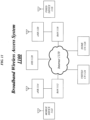
- FIG. 11 illustrates an embodiment of a broadband wireless access system 1100.
- broadband wireless access system 1100 may be an internet protocol (IP) type network comprising an internet 1110 type network or the like that is capable of supporting mobile wireless access and/or fixed wireless access to internet 1110.
- IP internet protocol
- broadband wireless access system 1100 may comprise any type of orthogonal frequency division multiple access (OFDMA)-based or single-carrier frequency division multiple access (SC-FDMA)-based wireless network, such as a system compliant with one or more of the 3GPP LTE Specifications and/or IEEE 802.16 Standards, and the scope of the claimed subject matter is not limited in these respects.
- OFDMA orthogonal frequency division multiple access
- SC-FDMA single-carrier frequency division multiple access
- radio access networks (RANs) 1112 and 1118 are capable of coupling with evolved node Bs (eNBs) 1114 and 1120, respectively, to provide wireless communication between one or more fixed devices 1116 and internet 1110 and/or between or one or more mobile devices 1122 and Internet 1110.
- RANs 1112 and 1118 may implement profiles that are capable of defining the mapping of network functions to one or more physical entities on broadband wireless access system 1100.
- eNBs 1114 and 1120 may comprise radio equipment to provide RF communication with fixed device 1116 and/or mobile device 1122, such as described with reference to device 1000, and may comprise, for example, the PHY and MAC layer equipment in compliance with a 3GPP LTE Specification or an IEEE 802.16 Standard. eNBs 1114 and 1120 may further comprise an IP backplane to couple to Internet 1110 via RANs 1112 and 1118, respectively, although the scope of the claimed subject matter is not limited in these respects.
- Broadband wireless access system 1100 may further comprise a visited core network (CN) 1124 and/or a home CN 1126, each of which may be capable of providing one or more network functions including but not limited to proxy and/or relay type functions, for example authentication, authorization and accounting (AAA) functions, dynamic host configuration protocol (DHCP) functions, or domain name service controls or the like, domain gateways such as public switched telephone network (PSTN) gateways or voice over internet protocol (VoIP) gateways, and/or internet protocol (IP) type server functions, or the like.
- AAA authentication, authorization and accounting
- DHCP dynamic host configuration protocol
- IP internet protocol
- these are merely example of the types of functions that are capable of being provided by visited CN 1124 and/or home CN 1126, and the scope of the claimed subject matter is not limited in these respects.
- Visited CN 1124 may be referred to as a visited CN in the case where visited CN 1124 is not part of the regular service provider of fixed device 1116 or mobile device 1122, for example where fixed device 1116 or mobile device 1122 is roaming away from its respective home CN 1126, or where broadband wireless access system 1100 is part of the regular service provider of fixed device 1116 or mobile device 1122 but where broadband wireless access system 1100 may be in another location or state that is not the main or home location of fixed device 1116 or mobile device 1122.
- the embodiments are not limited in this context.
- Fixed device 1116 may be located anywhere within range of one or both of eNBs 1114 and 1120, such as in or near a home or business to provide home or business customer broadband access to Internet 1110 via eNBs 1114 and 1120 and RANs 1112 and 1118, respectively, and home CN 1126. It is worthy of note that although fixed device 1116 is generally disposed in a stationary location, it may be moved to different locations as needed. Mobile device 1122 may be utilized at one or more locations if mobile device 1122 is within range of one or both of eNBs 1114 and 1120, for example.
- operation support system (OSS) 1128 may be part of broadband wireless access system 1100 to provide management functions for broadband wireless access system 1100 and to provide interfaces between functional entities of broadband wireless access system 1100.
- Broadband wireless access system 1100 of FIG. 11 is merely one type of wireless network showing a certain number of the components of broadband wireless access system 1100, and the scope of the claimed subject matter is not limited in these respects.
- Various embodiments may be implemented using hardware elements, software elements, or a combination of both.
- hardware elements may include processors, microprocessors, circuits, circuit elements (e.g., transistors, resistors, capacitors, inductors, and so forth), integrated circuits, application specific integrated circuits (ASIC), programmable logic devices (PLD), digital signal processors (DSP), field programmable gate array (FPGA), logic gates, registers, semiconductor device, chips, microchips, chip sets, and so forth.
- Examples of software may include software components, programs, applications, computer programs, application programs, system programs, machine programs, operating system software, middleware, firmware, software modules, routines, subroutines, functions, methods, procedures, software interfaces, application program interfaces (API), instruction sets, computing code, computer code, code segments, computer code segments, words, values, symbols, or any combination thereof. Determining whether an embodiment is implemented using hardware elements and/or software elements may vary in accordance with any number of factors, such as desired computational rate, power levels, heat tolerances, processing cycle budget, input data rates, output data rates, memory resources, data bus speeds and other design or performance constraints.
- One or more aspects of at least one embodiment may be implemented by representative instructions stored on a machine-readable medium which represents various logic within the processor, which when read by a machine causes the machine to fabricate logic to perform the techniques described herein.
- Such representations known as "IP cores" may be stored on a tangible, machine readable medium and supplied to various customers or manufacturing facilities to load into the fabrication machines that actually make the logic or processor.
- Some embodiments may be implemented, for example, using a machine-readable medium or article which may store an instruction or a set of instructions that, if executed by a machine, may cause the machine to perform a method and/or operations in accordance with the embodiments.
- Such a machine may include, for example, any suitable processing platform, computing platform, computing device, processing device, computing system, processing system, computer, processor, or the like, and may be implemented using any suitable combination of hardware and/or software.
- the machine-readable medium or article may include, for example, any suitable type of memory unit, memory device, memory article, memory medium, storage device, storage article, storage medium and/or storage unit, for example, memory, removable or non-removable media, erasable or non-erasable media, writeable or re-writeable media, digital or analog media, hard disk, floppy disk, Compact Disk Read Only Memory (CD-ROM), Compact Disk Recordable (CD-R), Compact Disk Rewriteable (CD-RW), optical disk, magnetic media, magneto-optical media, removable memory cards or disks, various types of Digital Versatile Disk (DVD), a tape, a cassette, or the like.
- CD-ROM Compact Disk Read Only Memory
- CD-R Compact Disk Recordable
- CD-RW Compact Dis
- the instructions may include any suitable type of code, such as source code, compiled code, interpreted code, executable code, static code, dynamic code, encrypted code, and the like, implemented using any suitable high-level, low-level, object-oriented, visual, compiled and/or interpreted programming language.
- Coupled and “connected” along with their derivatives. These terms are not intended as synonyms for each other. For example, some embodiments may be described using the terms “connected” and/or “coupled” to indicate that two or more elements are in direct physical or electrical contact with each other. The term “coupled,” however, may also mean that two or more elements are not in direct contact with each other, but yet still co-operate or interact with each other.
- processing refers to the action and/or processes of a computer or computing system, or similar electronic computing device, that manipulates and/or transforms data represented as physical quantities (e.g., electronic) within the computing system's registers and/or memories into other data similarly represented as physical quantities within the computing system's memories, registers or other such information storage, transmission or display devices.
- physical quantities e.g., electronic
Landscapes
- Engineering & Computer Science (AREA)
- Signal Processing (AREA)
- Computer Networks & Wireless Communication (AREA)
- Mobile Radio Communication Systems (AREA)
Claims (15)
- Vorrichtung, die Folgendes aufweist:einen Speicher; undLogik für ein Benutzergerät (104), UE, wobei wenigstens ein Teil der Logik in einer Basisbandschaltung implementiert ist, die mit dem Speicher gekoppelt ist, wobei die Logik Folgendes durchführt:Identifizieren eines Zwei-Bit-Feedback-Konfigurationsinformations-, HFCI-, Feldes (418), das in Downlink-Steuerinformationen, DCI, enthalten ist, die von einem entwickelten Knoten B, eNB, (102) empfangen werden,wobei das Zwei-Bit-HFCI-Feld ein Physical-Uplink-Control-Channel-, PUCCH-, Format und eine PUCCH-Ressource (116) oder eine Nutzlastgröße eines PUCCH-Formats und eines Hybrid-Automatic-Repeat-Request-, HARQ-, Feedbacks (214) für ein HARQ-Feedback angibt;Bestimmen einer Anzahl von Bits des HARQ-Feedbacks basierend auf der Nutzlastgröße des HARQ-Feedbacks oder basierend auf dem PUCCH-Format, die in Steuerinformationen einzuschließen sind, die einem entwickelten Knoten B (102), eNB, bereitgestellt werden;Bestimmen, ob ein PUCCH-Format 3 die Anzahl von Bits des HARQ-Feedbacks (214) aufnehmen kann; undals Reaktion auf eine Bestimmung, dass das PUCCH-Format 3 die Anzahl von Bits des HARQ-Feedbacks nicht aufnehmen kann:Erzeugen der Steuerinformationen gemäß einem zweiten PUCCH-Format; undSenden der Steuerinformationen an eine Hochfrequenz-, RF-, Schaltung (1010) zur Übertragung an den eNB (102) über die PUCCH-Ressource, die basierend auf dem Zwei-Bit-HFCI-Feld identifiziert wird.
- Vorrichtung nach Anspruch 1, wobei das Zwei-Bit-HFCI-Feld in einem Sendeleistungssteuerungs-, TPC-, Feld der DCI enthalten ist.
- Vorrichtung nach Anspruch 2, wobei das TPC-Feld ein 2-Bit-TPC-Feld ist, das in einer PDCCH-Zuweisung enthalten ist.
- Vorrichtung nach einem der Ansprüche 1 bis 3, wobei die Logik Folgendes durchführt:Identifizieren eines PUCCH-Ressourcenwerts, der dem Zwei-Bit-HFCI-Feld entspricht, das in den DCI enthalten ist; undIdentifizieren der PUCCH-Ressource (116) basierend auf dem PUCCH-Ressourcenwert.
- Vorrichtung nach einem der Ansprüche 1 bis 4, wobei die HARQ-Rückmeldung (214) eine Rückmeldung für Downlink-, DL, Datenübertragungen an die UE (104) über eine Vielzahl von aggregierten Komponententrägern aufweist.
- Vorrichtung nach einem der Ansprüche 1 bis 5, wobei die Logik bestimmt, dass das PUCCH-Format 3 die bestimmte Anzahl von Bits des HARQ-Feedbacks (214) nicht aufnehmen kann, wenn die bestimmte Anzahl von Bits des HARQ-Feedbacks 21 Bits überschreitet.
- Vorrichtung nach einem der Ansprüche 1 bis 6, wobei die Logik Folgendes durchführt:
als Reaktion auf eine Bestimmung, dass das PUCCH-Format 3 die bestimmte Anzahl von Bits des HARQ-Feedbacks (214) aufnehmen kann, Erzeugen der Steuerinformationen gemäß dem PUCCH-Format 3 zur Übertragung an den eNB (102) über eine PUCCH-Ressource (116), die basierend auf dem Zwei-Bit-HFCI-Feld identifiziert wird. - Vorrichtung nach einem der Ansprüche 1 bis 7, wobei die Logik die Steuerinformationen zur Übertragung an den eNB (102) über einen PUCCH (116) einer primären Zelle der UE (104) erzeugt.
- Vorrichtung nach einem der Ansprüche 1 bis 8, die eine Hochfrequenz-, RF-, Schaltung (1010) aufweist, die mit der Basisbandschaltung gekoppelt ist, wobei die RF-Schaltung RF-Signale zur Übertragung an den eNB (102) erzeugt, wobei die RF-Signale die Steuerinformationen aufweisen.
- Nicht-transitorisches computerlesbares Speichermedium, das einen Satz von Anweisungen aufweist, die als Reaktion darauf, dass sie an einem Benutzergerät (104), UE, ausgeführt werden, das UE zu Folgendem veranlassen:Identifizieren eines Zwei-Bit-Feedback-Konfigurationsinformations-, HFCI-, Feldes (418), das in Downlink-Steuerinformationen, DCI, enthalten ist, die von einem entwickelten Knoten B, eNB, (102) empfangen werden,wobei das Zwei-Bit-HFCI-Feld ein Physical-Uplink-Control-Channel-, PUCCH-, Format, eine PUCCH-Ressource (116) und eine Nutzlastgröße eines Hybrid-Automatic-Repeat-Request-, HARQ-, Feedbacks (214) für ein HARQ-Feedback angibt;Identifizieren eines Hybrid-Automatic-Repeat-Request-, HARQ-, Feedbacks, das dem eNB über einen PUCCH einer primären Zelle der UE gemäß einem PUCCH-Format bereitgestellt werden, das eine größere Anzahl von HARQ-Feedback-Bits aufnehmen kann, als durch ein PUCCH-Format 3 aufgenommen werden kann;Bestimmen, basierend auf dem Zwei-Bit-Feedback-HFCI-Feld, einer PUCCH-Ressource zum Bereitstellen des HARQ-Feedbacks; undErzeugen von Steuerinformationen gemäß dem PUCCH-Format zur Übertragung an die BS über die PUCCH-Ressource, wobei die Steuerinformationen das HARQ-Feedback aufweist.
- Nichtflüchtiges computerlesbares Speichermedium nach Anspruch 10, wobei die DCI von dem eNB (102) über einen Physical-Downlink-Control-Channel (108), PDCCH, oder einen Enhanced-Physical-Downlink-Control-Channel, EPDCCH, empfangen werden.
- Nichtflüchtiges computerlesbares Speichermedium nach einem der Ansprüche 10 bis 11, wobei ein Format der DCI eines von einem DeI-Format 1, einem DCI-Format 1A, einem DCI-Format 1B, einem DeI-Format 1D, einem DCI-Format 2, einem DCI-Format 2A, einem DCI-Format 2B, einem DeI-Format 2C und einem DCI-Format 2D aufweist.
- Nichtflüchtiges computerlesbares Speichermedium nach einem der Ansprüche 10 bis 12, das ein Bestimmen aufweist, dass das HARQ-Feedback (214) gemäß dem PUCCH-Format bereitgestellt wird, basierend auf einer Bestimmung, dass das HARQ-Feedback eine Anzahl von Bits aufweist, die durch das PUCCH-Format 3 nicht aufgenommen werden kann.
- Nichtflüchtiges computerlesbares Speichermedium nach einem der Ansprüche 10 bis 13, wobei das Zwei-Bit-HFCI-Feld ein zweites PUCCH-Format, eine dritte HARQ-Nutzlastgröße und einen dritten PUCCH angibt.
- Nichtflüchtiges computerlesbares Speichermedium nach Anspruch 14, wobei das Zwei-Bit-HFCI-Feld in einem Sendeleistungssteuerungs-, TPC-, Feld der DCI enthalten ist.
Applications Claiming Priority (2)
| Application Number | Priority Date | Filing Date | Title |
|---|---|---|---|
| US201562203673P | 2015-08-11 | 2015-08-11 | |
| PCT/US2015/000441 WO2017026979A1 (en) | 2015-08-11 | 2015-12-24 | Harq feedback configuration techniques for broadband wireless communication networks |
Publications (2)
| Publication Number | Publication Date |
|---|---|
| EP3335347A1 EP3335347A1 (de) | 2018-06-20 |
| EP3335347B1 true EP3335347B1 (de) | 2025-02-12 |
Family
ID=55182537
Family Applications (1)
| Application Number | Title | Priority Date | Filing Date |
|---|---|---|---|
| EP15826211.3A Active EP3335347B1 (de) | 2015-08-11 | 2015-12-24 | Harq-feedback-konfigurationstechniken für breitbandige drahtloskommunikationsnetzwerke |
Country Status (3)
| Country | Link |
|---|---|
| US (1) | US11146375B2 (de) |
| EP (1) | EP3335347B1 (de) |
| WO (1) | WO2017026979A1 (de) |
Families Citing this family (11)
| Publication number | Priority date | Publication date | Assignee | Title |
|---|---|---|---|---|
| US10966236B2 (en) * | 2017-03-23 | 2021-03-30 | Apple Inc. | Scheduling and hybrid automatic repeat request operation for carrier aggregation with mixed numerologies |
| US10506468B2 (en) * | 2017-09-08 | 2019-12-10 | At&T Intellectual Property I, L.P. | Reporting hybrid automatic repeat request-acknowledgements in wireless communication systems |
| EP3982575B1 (de) * | 2017-10-11 | 2026-05-20 | Ericsson Telefon Ab L M | Bestätigungssignalisierungsverfahren für funkzugangsnetzwerke |
| US11297674B2 (en) * | 2018-02-14 | 2022-04-05 | Samsung Electronics Co., Ltd. | Method and apparatus for power savings at a user equipment |
| KR20200050812A (ko) * | 2018-11-02 | 2020-05-12 | 삼성전자주식회사 | 무선 통신 시스템에서 데이터 및 피드백의 송수신을 수행하는 방법 및 장치 |
| WO2020133504A1 (zh) * | 2018-12-29 | 2020-07-02 | 北京小米移动软件有限公司 | 直连通信的数据传输方法、装置、设备及系统 |
| US11375476B2 (en) * | 2019-10-01 | 2022-06-28 | Qualcomm Incorporated | Sidelink feedback transmission with multiple feedback timelines |
| WO2021189382A1 (en) * | 2020-03-26 | 2021-09-30 | Nokia Shanghai Bell Co., Ltd. | Scheduling release feedback |
| WO2021226968A1 (en) * | 2020-05-14 | 2021-11-18 | Apple Inc. | Uplink control information transmission in wireless communication |
| CN115804202B (zh) * | 2020-07-27 | 2024-07-09 | Oppo广东移动通信有限公司 | 无线通信方法、终端设备和网络设备 |
| US11792803B2 (en) * | 2021-01-25 | 2023-10-17 | Qualcomm Incorporated | Methods and apparatus for utilizing UL symbols for deferred SPS HARQ-ACK transmissions |
Family Cites Families (25)
| Publication number | Priority date | Publication date | Assignee | Title |
|---|---|---|---|---|
| CN101981854A (zh) | 2008-03-25 | 2011-02-23 | 诺基亚公司 | 在具有NxPDCCH结构的LTE-A TDD中的PUCCH上的ACK/NACK传输 |
| KR101902410B1 (ko) * | 2009-07-16 | 2018-09-28 | 엘지전자 주식회사 | 무선 통신 시스템에서 수신 장치가 제어 정보를 전송하는 방법 |
| KR101832771B1 (ko) * | 2010-09-15 | 2018-02-27 | 엘지전자 주식회사 | 무선 통신 시스템에서의 제어 정보의 전송 방법 및 장치 |
| CN102098151B (zh) * | 2010-12-28 | 2015-08-12 | 中兴通讯股份有限公司 | 一种正确/错误应答消息的发送方法及用户终端 |
| WO2013025005A2 (ko) * | 2011-08-12 | 2013-02-21 | 엘지전자 주식회사 | 무선 통신 시스템에서 상향링크 제어 채널을 위한 자원을 획득하는 방법 및 장치 |
| WO2013062396A1 (ko) * | 2011-10-27 | 2013-05-02 | 엘지전자 주식회사 | 상향링크를 통한 제어 정보 전송하는 방법 및 장치 |
| CN103095433B (zh) * | 2011-11-04 | 2018-06-15 | 北京三星通信技术研究有限公司 | 一种发送harq-ack反馈信息的方法 |
| CN103095432A (zh) * | 2011-11-07 | 2013-05-08 | 北京三星通信技术研究有限公司 | 一种发送harq-ack反馈信息的方法 |
| US8958331B2 (en) * | 2012-07-02 | 2015-02-17 | Intel Corporation | HARQ-ACK handling for unintended downlink sub-frames |
| CN103582008A (zh) * | 2012-07-26 | 2014-02-12 | 北京三星通信技术研究有限公司 | 一种在业务流量自适应tdd系统中传输harq-ack反馈信息的方法 |
| US10314015B2 (en) * | 2012-10-26 | 2019-06-04 | Intel Corporation | Reporting of user plan congestion |
| US9112662B2 (en) | 2013-01-17 | 2015-08-18 | Samsung Electronics Co., Ltd. | Overhead reduction for transmission of acknowledgment signals |
| US20140328260A1 (en) * | 2013-02-26 | 2014-11-06 | Samsung Electronics Co., Ltd. | Scheduling over multiple transmission time intervals |
| WO2014157993A1 (en) | 2013-03-28 | 2014-10-02 | Samsung Electronics Co., Ltd. | Aggregation of fdd and tdd cells |
| US9838161B2 (en) * | 2013-09-27 | 2017-12-05 | Nokia Solutions And Networks Oy | Bundling HARQ feedback in a time division duplexing communication system |
| US9473289B2 (en) * | 2013-09-27 | 2016-10-18 | Nokia Solutions And Networks Oy | PUCCH resource allocation and use |
| CN105814827B (zh) * | 2013-10-30 | 2019-06-11 | Lg 电子株式会社 | 从同时接入多小区的用户设备发送harq ack/nack的方法 |
| KR20150051063A (ko) * | 2013-11-01 | 2015-05-11 | 주식회사 아이티엘 | 하향링크 harq-ack와 sr동시 전송 방법 및 장치 |
| CA2942934C (en) * | 2014-03-21 | 2019-02-12 | Nokia Solutions And Networks Oy | Method and apparatus for deriving secondary cell hybrid-automatic-repeat-request timing |
| US10492216B2 (en) * | 2014-09-24 | 2019-11-26 | Telefonaktiebolaget Lm Ericsson (Publ) | Method and BS for scheduling UE, and method and UE for transmitting HARQ |
| US9686064B2 (en) * | 2015-01-21 | 2017-06-20 | Intel IP Corporation | Devices and methods for HARQ-ACK feedback scheme on PUSCH in wireless communication systems |
| US11362759B2 (en) * | 2015-04-06 | 2022-06-14 | Samsung Electronics Co., Ltd. | Transmission power control for an uplink control channel |
| US9888465B2 (en) * | 2015-04-06 | 2018-02-06 | Samsung Electronics Co., Ltd. | Codeword determination for acknowledgement information |
| CN106301670A (zh) * | 2015-05-15 | 2017-01-04 | 中兴通讯股份有限公司 | 上行控制信息的发送方法及装置 |
| WO2017023146A1 (en) * | 2015-08-06 | 2017-02-09 | Innovative Technology Lab Co., Ltd. | Apparatus and method for transmitting uplink control information through a physical uplink control channel |
-
2015
- 2015-12-24 EP EP15826211.3A patent/EP3335347B1/de active Active
- 2015-12-24 WO PCT/US2015/000441 patent/WO2017026979A1/en not_active Ceased
- 2015-12-24 US US15/751,451 patent/US11146375B2/en active Active
Also Published As
| Publication number | Publication date |
|---|---|
| WO2017026979A1 (en) | 2017-02-16 |
| EP3335347A1 (de) | 2018-06-20 |
| US20200204328A1 (en) | 2020-06-25 |
| US11146375B2 (en) | 2021-10-12 |
Similar Documents
| Publication | Publication Date | Title |
|---|---|---|
| US11146375B2 (en) | HARQ feedback configuration techniques for broadband wireless communication networks | |
| US11336414B2 (en) | Downlink hybrid automatic repeat request feedback for narrowband Internet of Things devices | |
| US11251907B2 (en) | Contention window size adaptation | |
| US12028847B2 (en) | Latency reduction techniques for radio access networks | |
| CN108702238B (zh) | 在物理上行链路共享信道上复用上行链路控制信息和数据 | |
| US10667294B2 (en) | Carrier-sensing techniques for LTE-based transmissions over unlicensed carriers | |
| US20230024287A1 (en) | Scheduling and hybrid automatic repeat request operation and codebook design for new radio carrier aggregation | |
| EP3348012B1 (de) | Übertragung von mehreren harq-ack-rückkopplungsbits entsprechend mehreren downlink-zellen und einem oder zwei transportblöcken pro zelle | |
| TWI815792B (zh) | 混合開迴路和閉迴路波束成形 | |
| WO2017091244A1 (en) | Hybrid arq schemes based on low density parity check codes | |
| WO2017136004A1 (en) | Systems and methods for flexible time-domain resource mapping for npdcch and npdsch in nb-iot systems | |
| HK1262372A1 (en) | Multiplexing uplink control information and data on physical uplink shared channel | |
| HK1262372B (zh) | 在物理上行链路共享信道上复用上行链路控制信息和数据 | |
| HK1262241A1 (en) | Hybrid open-loop and closed-loop beamforming | |
| HK1252882B (zh) | 无线系统中的上行链路控制信息的传输 |
Legal Events
| Date | Code | Title | Description |
|---|---|---|---|
| STAA | Information on the status of an ep patent application or granted ep patent |
Free format text: STATUS: THE INTERNATIONAL PUBLICATION HAS BEEN MADE |
|
| PUAI | Public reference made under article 153(3) epc to a published international application that has entered the european phase |
Free format text: ORIGINAL CODE: 0009012 |
|
| STAA | Information on the status of an ep patent application or granted ep patent |
Free format text: STATUS: REQUEST FOR EXAMINATION WAS MADE |
|
| 17P | Request for examination filed |
Effective date: 20180120 |
|
| AK | Designated contracting states |
Kind code of ref document: A1 Designated state(s): AL AT BE BG CH CY CZ DE DK EE ES FI FR GB GR HR HU IE IS IT LI LT LU LV MC MK MT NL NO PL PT RO RS SE SI SK SM TR |
|
| AX | Request for extension of the european patent |
Extension state: BA ME |
|
| RIN1 | Information on inventor provided before grant (corrected) |
Inventor name: KWON, HWAN-JOON Inventor name: XIONG, GANG Inventor name: HE, HONG Inventor name: HAN, SEUNGHEE Inventor name: DAVYDOV, ALEXEI |
|
| DAV | Request for validation of the european patent (deleted) | ||
| DAX | Request for extension of the european patent (deleted) | ||
| RAP1 | Party data changed (applicant data changed or rights of an application transferred) |
Owner name: APPLE INC. |
|
| STAA | Information on the status of an ep patent application or granted ep patent |
Free format text: STATUS: EXAMINATION IS IN PROGRESS |
|
| 17Q | First examination report despatched |
Effective date: 20210712 |
|
| GRAP | Despatch of communication of intention to grant a patent |
Free format text: ORIGINAL CODE: EPIDOSNIGR1 |
|
| STAA | Information on the status of an ep patent application or granted ep patent |
Free format text: STATUS: GRANT OF PATENT IS INTENDED |
|
| INTG | Intention to grant announced |
Effective date: 20240906 |
|
| RIN1 | Information on inventor provided before grant (corrected) |
Inventor name: KWON, HWAN-JOON Inventor name: XIONG, GANG Inventor name: HAN, SEUNGHEE Inventor name: DAVYDOV, ALEXEI Inventor name: HE, HONG |
|
| GRAS | Grant fee paid |
Free format text: ORIGINAL CODE: EPIDOSNIGR3 |
|
| GRAA | (expected) grant |
Free format text: ORIGINAL CODE: 0009210 |
|
| STAA | Information on the status of an ep patent application or granted ep patent |
Free format text: STATUS: THE PATENT HAS BEEN GRANTED |
|
| AK | Designated contracting states |
Kind code of ref document: B1 Designated state(s): AL AT BE BG CH CY CZ DE DK EE ES FI FR GB GR HR HU IE IS IT LI LT LU LV MC MK MT NL NO PL PT RO RS SE SI SK SM TR |
|
| REG | Reference to a national code |
Ref country code: GB Ref legal event code: FG4D |
|
| REG | Reference to a national code |
Ref country code: CH Ref legal event code: EP |
|
| REG | Reference to a national code |
Ref country code: DE Ref legal event code: R096 Ref document number: 602015090998 Country of ref document: DE |
|
| REG | Reference to a national code |
Ref country code: IE Ref legal event code: FG4D |
|
| REG | Reference to a national code |
Ref country code: NL Ref legal event code: MP Effective date: 20250212 |
|
| PG25 | Lapsed in a contracting state [announced via postgrant information from national office to epo] |
Ref country code: RS Free format text: LAPSE BECAUSE OF FAILURE TO SUBMIT A TRANSLATION OF THE DESCRIPTION OR TO PAY THE FEE WITHIN THE PRESCRIBED TIME-LIMIT Effective date: 20250512 |
|
| PG25 | Lapsed in a contracting state [announced via postgrant information from national office to epo] |
Ref country code: FI Free format text: LAPSE BECAUSE OF FAILURE TO SUBMIT A TRANSLATION OF THE DESCRIPTION OR TO PAY THE FEE WITHIN THE PRESCRIBED TIME-LIMIT Effective date: 20250212 |
|
| PG25 | Lapsed in a contracting state [announced via postgrant information from national office to epo] |
Ref country code: PL Free format text: LAPSE BECAUSE OF FAILURE TO SUBMIT A TRANSLATION OF THE DESCRIPTION OR TO PAY THE FEE WITHIN THE PRESCRIBED TIME-LIMIT Effective date: 20250212 |
|
| PG25 | Lapsed in a contracting state [announced via postgrant information from national office to epo] |
Ref country code: ES Free format text: LAPSE BECAUSE OF FAILURE TO SUBMIT A TRANSLATION OF THE DESCRIPTION OR TO PAY THE FEE WITHIN THE PRESCRIBED TIME-LIMIT Effective date: 20250212 |
|
| REG | Reference to a national code |
Ref country code: LT Ref legal event code: MG9D |
|
| PG25 | Lapsed in a contracting state [announced via postgrant information from national office to epo] |
Ref country code: IS Free format text: LAPSE BECAUSE OF FAILURE TO SUBMIT A TRANSLATION OF THE DESCRIPTION OR TO PAY THE FEE WITHIN THE PRESCRIBED TIME-LIMIT Effective date: 20250612 Ref country code: NO Free format text: LAPSE BECAUSE OF FAILURE TO SUBMIT A TRANSLATION OF THE DESCRIPTION OR TO PAY THE FEE WITHIN THE PRESCRIBED TIME-LIMIT Effective date: 20250512 |
|
| PG25 | Lapsed in a contracting state [announced via postgrant information from national office to epo] |
Ref country code: NL Free format text: LAPSE BECAUSE OF FAILURE TO SUBMIT A TRANSLATION OF THE DESCRIPTION OR TO PAY THE FEE WITHIN THE PRESCRIBED TIME-LIMIT Effective date: 20250212 |
|
| PG25 | Lapsed in a contracting state [announced via postgrant information from national office to epo] |
Ref country code: HR Free format text: LAPSE BECAUSE OF FAILURE TO SUBMIT A TRANSLATION OF THE DESCRIPTION OR TO PAY THE FEE WITHIN THE PRESCRIBED TIME-LIMIT Effective date: 20250212 |
|
| PG25 | Lapsed in a contracting state [announced via postgrant information from national office to epo] |
Ref country code: PT Free format text: LAPSE BECAUSE OF FAILURE TO SUBMIT A TRANSLATION OF THE DESCRIPTION OR TO PAY THE FEE WITHIN THE PRESCRIBED TIME-LIMIT Effective date: 20250612 Ref country code: LV Free format text: LAPSE BECAUSE OF FAILURE TO SUBMIT A TRANSLATION OF THE DESCRIPTION OR TO PAY THE FEE WITHIN THE PRESCRIBED TIME-LIMIT Effective date: 20250212 |
|
| PG25 | Lapsed in a contracting state [announced via postgrant information from national office to epo] |
Ref country code: BG Free format text: LAPSE BECAUSE OF FAILURE TO SUBMIT A TRANSLATION OF THE DESCRIPTION OR TO PAY THE FEE WITHIN THE PRESCRIBED TIME-LIMIT Effective date: 20250212 Ref country code: GR Free format text: LAPSE BECAUSE OF FAILURE TO SUBMIT A TRANSLATION OF THE DESCRIPTION OR TO PAY THE FEE WITHIN THE PRESCRIBED TIME-LIMIT Effective date: 20250513 |
|
| REG | Reference to a national code |
Ref country code: AT Ref legal event code: MK05 Ref document number: 1767127 Country of ref document: AT Kind code of ref document: T Effective date: 20250212 |
|
| PG25 | Lapsed in a contracting state [announced via postgrant information from national office to epo] |
Ref country code: SE Free format text: LAPSE BECAUSE OF FAILURE TO SUBMIT A TRANSLATION OF THE DESCRIPTION OR TO PAY THE FEE WITHIN THE PRESCRIBED TIME-LIMIT Effective date: 20250212 |
|
| PG25 | Lapsed in a contracting state [announced via postgrant information from national office to epo] |
Ref country code: SM Free format text: LAPSE BECAUSE OF FAILURE TO SUBMIT A TRANSLATION OF THE DESCRIPTION OR TO PAY THE FEE WITHIN THE PRESCRIBED TIME-LIMIT Effective date: 20250212 |
|
| PG25 | Lapsed in a contracting state [announced via postgrant information from national office to epo] |
Ref country code: DK Free format text: LAPSE BECAUSE OF FAILURE TO SUBMIT A TRANSLATION OF THE DESCRIPTION OR TO PAY THE FEE WITHIN THE PRESCRIBED TIME-LIMIT Effective date: 20250212 |
|
| PG25 | Lapsed in a contracting state [announced via postgrant information from national office to epo] |
Ref country code: IT Free format text: LAPSE BECAUSE OF FAILURE TO SUBMIT A TRANSLATION OF THE DESCRIPTION OR TO PAY THE FEE WITHIN THE PRESCRIBED TIME-LIMIT Effective date: 20250212 |
|
| PG25 | Lapsed in a contracting state [announced via postgrant information from national office to epo] |
Ref country code: AT Free format text: LAPSE BECAUSE OF FAILURE TO SUBMIT A TRANSLATION OF THE DESCRIPTION OR TO PAY THE FEE WITHIN THE PRESCRIBED TIME-LIMIT Effective date: 20250212 |
|
| PG25 | Lapsed in a contracting state [announced via postgrant information from national office to epo] |
Ref country code: CZ Free format text: LAPSE BECAUSE OF FAILURE TO SUBMIT A TRANSLATION OF THE DESCRIPTION OR TO PAY THE FEE WITHIN THE PRESCRIBED TIME-LIMIT Effective date: 20250212 Ref country code: EE Free format text: LAPSE BECAUSE OF FAILURE TO SUBMIT A TRANSLATION OF THE DESCRIPTION OR TO PAY THE FEE WITHIN THE PRESCRIBED TIME-LIMIT Effective date: 20250212 |
|
| PG25 | Lapsed in a contracting state [announced via postgrant information from national office to epo] |
Ref country code: RO Free format text: LAPSE BECAUSE OF FAILURE TO SUBMIT A TRANSLATION OF THE DESCRIPTION OR TO PAY THE FEE WITHIN THE PRESCRIBED TIME-LIMIT Effective date: 20250212 |
|
| PG25 | Lapsed in a contracting state [announced via postgrant information from national office to epo] |
Ref country code: SK Free format text: LAPSE BECAUSE OF FAILURE TO SUBMIT A TRANSLATION OF THE DESCRIPTION OR TO PAY THE FEE WITHIN THE PRESCRIBED TIME-LIMIT Effective date: 20250212 |
|
| REG | Reference to a national code |
Ref country code: DE Ref legal event code: R097 Ref document number: 602015090998 Country of ref document: DE |
|
| PLBE | No opposition filed within time limit |
Free format text: ORIGINAL CODE: 0009261 |
|
| STAA | Information on the status of an ep patent application or granted ep patent |
Free format text: STATUS: NO OPPOSITION FILED WITHIN TIME LIMIT |
|
| PGFP | Annual fee paid to national office [announced via postgrant information from national office to epo] |
Ref country code: DE Payment date: 20250930 Year of fee payment: 11 |
|
| 26N | No opposition filed |
Effective date: 20251113 |