EP3333620A1 - Display device provided with touch keys - Google Patents
Display device provided with touch keys Download PDFInfo
- Publication number
- EP3333620A1 EP3333620A1 EP16202831.0A EP16202831A EP3333620A1 EP 3333620 A1 EP3333620 A1 EP 3333620A1 EP 16202831 A EP16202831 A EP 16202831A EP 3333620 A1 EP3333620 A1 EP 3333620A1
- Authority
- EP
- European Patent Office
- Prior art keywords
- electrode
- liquid crystal
- front substrate
- structured
- electrically conductive
- Prior art date
- Legal status (The legal status is an assumption and is not a legal conclusion. Google has not performed a legal analysis and makes no representation as to the accuracy of the status listed.)
- Granted
Links
- 239000000758 substrate Substances 0.000 claims abstract description 61
- 239000004973 liquid crystal related substance Substances 0.000 claims abstract description 53
- 230000003287 optical effect Effects 0.000 claims abstract description 10
- 238000007789 sealing Methods 0.000 claims abstract description 6
- 239000012780 transparent material Substances 0.000 claims abstract description 5
- 239000011241 protective layer Substances 0.000 claims abstract description 3
- 239000004020 conductor Substances 0.000 abstract description 6
- 238000004519 manufacturing process Methods 0.000 description 10
- 238000000034 method Methods 0.000 description 4
- 239000000463 material Substances 0.000 description 3
- PEDCQBHIVMGVHV-UHFFFAOYSA-N Glycerine Chemical compound OCC(O)CO PEDCQBHIVMGVHV-UHFFFAOYSA-N 0.000 description 2
- 239000004988 Nematic liquid crystal Substances 0.000 description 2
- 238000005530 etching Methods 0.000 description 2
- MRNHPUHPBOKKQT-UHFFFAOYSA-N indium;tin;hydrate Chemical compound O.[In].[Sn] MRNHPUHPBOKKQT-UHFFFAOYSA-N 0.000 description 2
- 239000010410 layer Substances 0.000 description 2
- 238000000206 photolithography Methods 0.000 description 2
- RYGMFSIKBFXOCR-UHFFFAOYSA-N Copper Chemical compound [Cu] RYGMFSIKBFXOCR-UHFFFAOYSA-N 0.000 description 1
- 241000283070 Equus zebra Species 0.000 description 1
- 239000012790 adhesive layer Substances 0.000 description 1
- 239000003990 capacitor Substances 0.000 description 1
- 230000000295 complement effect Effects 0.000 description 1
- 229910052802 copper Inorganic materials 0.000 description 1
- 239000010949 copper Substances 0.000 description 1
- 238000000151 deposition Methods 0.000 description 1
- 230000000994 depressogenic effect Effects 0.000 description 1
- 229920001971 elastomer Polymers 0.000 description 1
- 239000000806 elastomer Substances 0.000 description 1
- 230000005611 electricity Effects 0.000 description 1
- 230000005672 electromagnetic field Effects 0.000 description 1
- AMGQUBHHOARCQH-UHFFFAOYSA-N indium;oxotin Chemical compound [In].[Sn]=O AMGQUBHHOARCQH-UHFFFAOYSA-N 0.000 description 1
- 238000012986 modification Methods 0.000 description 1
- 230000004048 modification Effects 0.000 description 1
- 230000010287 polarization Effects 0.000 description 1
Images

Classifications
-
- G—PHYSICS
- G02—OPTICS
- G02F—OPTICAL DEVICES OR ARRANGEMENTS FOR THE CONTROL OF LIGHT BY MODIFICATION OF THE OPTICAL PROPERTIES OF THE MEDIA OF THE ELEMENTS INVOLVED THEREIN; NON-LINEAR OPTICS; FREQUENCY-CHANGING OF LIGHT; OPTICAL LOGIC ELEMENTS; OPTICAL ANALOGUE/DIGITAL CONVERTERS
- G02F1/00—Devices or arrangements for the control of the intensity, colour, phase, polarisation or direction of light arriving from an independent light source, e.g. switching, gating or modulating; Non-linear optics
- G02F1/01—Devices or arrangements for the control of the intensity, colour, phase, polarisation or direction of light arriving from an independent light source, e.g. switching, gating or modulating; Non-linear optics for the control of the intensity, phase, polarisation or colour
- G02F1/13—Devices or arrangements for the control of the intensity, colour, phase, polarisation or direction of light arriving from an independent light source, e.g. switching, gating or modulating; Non-linear optics for the control of the intensity, phase, polarisation or colour based on liquid crystals, e.g. single liquid crystal display cells
- G02F1/133—Constructional arrangements; Operation of liquid crystal cells; Circuit arrangements
- G02F1/1333—Constructional arrangements; Manufacturing methods
- G02F1/13338—Input devices, e.g. touch panels
-
- G—PHYSICS
- G02—OPTICS
- G02F—OPTICAL DEVICES OR ARRANGEMENTS FOR THE CONTROL OF LIGHT BY MODIFICATION OF THE OPTICAL PROPERTIES OF THE MEDIA OF THE ELEMENTS INVOLVED THEREIN; NON-LINEAR OPTICS; FREQUENCY-CHANGING OF LIGHT; OPTICAL LOGIC ELEMENTS; OPTICAL ANALOGUE/DIGITAL CONVERTERS
- G02F1/00—Devices or arrangements for the control of the intensity, colour, phase, polarisation or direction of light arriving from an independent light source, e.g. switching, gating or modulating; Non-linear optics
- G02F1/01—Devices or arrangements for the control of the intensity, colour, phase, polarisation or direction of light arriving from an independent light source, e.g. switching, gating or modulating; Non-linear optics for the control of the intensity, phase, polarisation or colour
- G02F1/13—Devices or arrangements for the control of the intensity, colour, phase, polarisation or direction of light arriving from an independent light source, e.g. switching, gating or modulating; Non-linear optics for the control of the intensity, phase, polarisation or colour based on liquid crystals, e.g. single liquid crystal display cells
- G02F1/133—Constructional arrangements; Operation of liquid crystal cells; Circuit arrangements
- G02F1/1333—Constructional arrangements; Manufacturing methods
- G02F1/1345—Conductors connecting electrodes to cell terminals
- G02F1/13452—Conductors connecting driver circuitry and terminals of panels
-
- G—PHYSICS
- G06—COMPUTING; CALCULATING OR COUNTING
- G06F—ELECTRIC DIGITAL DATA PROCESSING
- G06F3/00—Input arrangements for transferring data to be processed into a form capable of being handled by the computer; Output arrangements for transferring data from processing unit to output unit, e.g. interface arrangements
- G06F3/01—Input arrangements or combined input and output arrangements for interaction between user and computer
- G06F3/03—Arrangements for converting the position or the displacement of a member into a coded form
- G06F3/041—Digitisers, e.g. for touch screens or touch pads, characterised by the transducing means
- G06F3/0412—Digitisers structurally integrated in a display
-
- G—PHYSICS
- G06—COMPUTING; CALCULATING OR COUNTING
- G06F—ELECTRIC DIGITAL DATA PROCESSING
- G06F3/00—Input arrangements for transferring data to be processed into a form capable of being handled by the computer; Output arrangements for transferring data from processing unit to output unit, e.g. interface arrangements
- G06F3/01—Input arrangements or combined input and output arrangements for interaction between user and computer
- G06F3/03—Arrangements for converting the position or the displacement of a member into a coded form
- G06F3/041—Digitisers, e.g. for touch screens or touch pads, characterised by the transducing means
- G06F3/0416—Control or interface arrangements specially adapted for digitisers
- G06F3/04164—Connections between sensors and controllers, e.g. routing lines between electrodes and connection pads
-
- G—PHYSICS
- G06—COMPUTING; CALCULATING OR COUNTING
- G06F—ELECTRIC DIGITAL DATA PROCESSING
- G06F3/00—Input arrangements for transferring data to be processed into a form capable of being handled by the computer; Output arrangements for transferring data from processing unit to output unit, e.g. interface arrangements
- G06F3/01—Input arrangements or combined input and output arrangements for interaction between user and computer
- G06F3/03—Arrangements for converting the position or the displacement of a member into a coded form
- G06F3/041—Digitisers, e.g. for touch screens or touch pads, characterised by the transducing means
- G06F3/044—Digitisers, e.g. for touch screens or touch pads, characterised by the transducing means by capacitive means
- G06F3/0443—Digitisers, e.g. for touch screens or touch pads, characterised by the transducing means by capacitive means using a single layer of sensing electrodes
Landscapes
- Engineering & Computer Science (AREA)
- Physics & Mathematics (AREA)
- Theoretical Computer Science (AREA)
- General Engineering & Computer Science (AREA)
- General Physics & Mathematics (AREA)
- Nonlinear Science (AREA)
- Human Computer Interaction (AREA)
- Crystallography & Structural Chemistry (AREA)
- Optics & Photonics (AREA)
- Chemical & Material Sciences (AREA)
- Mathematical Physics (AREA)
- Computer Networks & Wireless Communication (AREA)
- Liquid Crystal (AREA)
- Devices For Indicating Variable Information By Combining Individual Elements (AREA)
Abstract
L'invention concerne un dispositif d'affichage à cristal liquide comprenant un substrat avant (2) et un substrat arrière (4) qui s'étend parallèlement à et à distance du substrat avant (2), les substrats avant (2) et arrière (4) étant réunis entre eux au moyen d'un cadre de scellement (8) qui délimite une enceinte étanche (10) pour le confinement d'un cristal liquide, au moins une première électrode (12) étant structurée sur une face inférieure (14) du substrat avant (2), et au moins une deuxième électrode (16) opposée étant structurée sur une face supérieure (18) du substrat arrière (6), les propriétés optiques du cristal liquide étant modifiées par application d'une tension électrique appropriée au point de croisement de la première et de la deuxième électrodes (12, 16) considérées, la au moins une première électrode (12) et la au moins une deuxième électrode (16) étant réalisées en un matériau transparent électriquement conducteur et étant prolongées vers l'extérieur du dispositif d'affichage à cristal liquide (1) par une première, respectivement une deuxième pistes électriquement conductrices (20, 14) structurées sur la face inférieure (14) du substrat avant (2), au moins une troisième électrode (26) définissant une zone tactile capacitive étant structurée sur une face supérieure (28) du substrat avant (2), cette troisième électrode (26) étant réalisée en un matériau transparent électriquement conducteur et étant prolongée par une troisième piste électriquement conductrice (32) avec laquelle une broche de connexion (40) est en contact électrique pour relier la troisième électrode (26) avec un dispositif extérieur de commande (30), au moins une couche de protection ou un polariseur (34) étant fixé sur la face supérieure (28) du substrat avant (2) et recouvrant la troisième électrode (26).The invention relates to a liquid crystal display device comprising a front substrate (2) and a rear substrate (4) which extends parallel to and away from the front substrate (2), the front (2) and rear substrates (4) being joined together by means of a sealing frame (8) which delimits a sealed enclosure (10) for the confinement of a liquid crystal, at least a first electrode (12) being structured on a lower face ( 14) of the front substrate (2), and at least one second opposite electrode (16) being structured on an upper face (18) of the rear substrate (6), the optical properties of the liquid crystal being modified by applying a voltage appropriate at the point of intersection of the first and second electrodes (12, 16) considered, the at least one first electrode (12) and the at least one second electrode (16) being made of a transparent electrically conductive material and being extended towards the outside of the liquid crystal display device (1) by a first, respectively a second electrically conductive tracks (20, 14) structured on the underside (14) of the front substrate (2), at least a third electrode (26) defining a capacitive touch zone being structured on an upper face (28) of the front substrate (2), this third electrode (26) being made of an electrically conductive transparent material and being extended by a third electrically conductive track (32). ) with which a connection pin (40) is in electrical contact for connecting the third electrode (26) with an external control device (30), at least one protective layer or a polarizer (34) being fixed on the upper face (28) of the front substrate (2) and covering the third electrode (26).
Description
La présente invention concerne un dispositif d'affichage muni de touches tactiles. La présente invention concerne tout particulièrement un dispositif d'affichage du type à cristal liquide comprenant de telles touches tactiles.The present invention relates to a display device with touch keys. The present invention particularly relates to a display device of the liquid crystal type comprising such tactile keys.
Dans son acception la plus simple, une cellule d'affichage à cristal liquide comprend un substrat avant orienté du côté de l'observateur et un substrat arrière qui s'étend parallèlement à et à distance du substrat avant. Les substrats avant et arrière sont réunis entre eux au moyen d'un cadre de scellement qui délimite une enceinte étanche pour le confinement d'un cristal liquide. Une surface inférieure du substrat avant porte au moins une électrode et une surface supérieure du substrat arrière porte au moins une contre-électrode correspondante. Par application d'une tension électrique appropriée entre l'électrode et la contre-électrode, il est possible de modifier les propriétés optiques du cristal liquide au point de croisement des électrodes considérées.In its simplest sense, a liquid crystal display cell comprises a front substrate oriented on the observer side and a rear substrate that extends parallel to and away from the front substrate. The front and rear substrates are joined together by means of a sealing frame which delimits a sealed enclosure for the confinement of a liquid crystal. A lower surface of the front substrate carries at least one electrode and an upper surface of the rear substrate carries at least one corresponding counter electrode. By applying a suitable voltage between the electrode and the counter-electrode, it is possible to modify the optical properties of the liquid crystal at the crossing point of the electrodes in question.
Il est déjà connu d'associer à un dispositif d'affichage à cristal liquide du type brièvement décrit ci-dessus un dispositif d'introduction de données de commande du type à touches tactiles. Un tel dispositif d'introduction de données comprend typiquement un film souple ou rigide sur une surface inférieure duquel sont structurées des touches de commande tactiles qui sont réalisées au moyen d'un matériau conducteur tel que de l'oxyde d'étain- indium, également connu sous sa dénomination anglo-saxonne Indium-Tin Oxyde ou ITO. Chacune de ces touches tactiles forme une armature d'un condensateur dont l'autre armature est formée par la portion d'une surface supérieure du film souple ou rigide qui fait face à la touche tactile. Par apposition d'un doigt sur l'une de ces touches tactiles, l'utilisateur modifie la valeur de la capacité détectée par cette touche tactile, ce qui provoque l'introduction d'un signal de commande dans un microcontrôleur auquel les touches tactiles du dispositif d'introduction de données sont classiquement reliées au moyen d'un câble de connexion souple. Une fois fabriqué, le dispositif d'introduction de données à touches tactiles est classiquement solidarisé par laminage sur la surface supérieure du substrat avant du dispositif d'affichage à cristal liquide.It is already known to associate with a liquid crystal display device of the type briefly described above a device for inputting control data of the touch-sensitive type. Such a data input device typically comprises a flexible or rigid film on a lower surface of which are structured touch control keys which are made by means of a conductive material such as tin-indium oxide, also known by its Anglo-Saxon name Indium-Tin Oxide or ITO. Each of these tactile keys forms an armature of a capacitor whose other armature is formed by the portion of an upper surface of the flexible or rigid film that faces the touch key. By placing a finger on one of these touch keys, the user modifies the value of the capacity detected by this touch key, which causes the introduction of a control signal in a microcontroller to which the touch keys of the data input device are conventionally connected by means of a flexible connection cable. Once fabricated, the touch-sensitive data input device is typically laminated to the upper surface of the front substrate of the liquid crystal display device.
L'un des intérêts du montage ci-dessus est qu'il permet de proposer un ensemble d'affichage et de commande monobloc que l'on peut aisément intégrer par exemple dans le volume de la boîte d'un objet portable tel qu'une montre-bracelet. Toutefois, les coûts de fabrication d'un tel ensemble d'affichage et de commande sont relativement élevés. Il faut en effet fabriquer séparément le dispositif d'affichage à cristal liquide et le dispositif de commande à touches tactiles, puis assembler ces deux éléments.One of the interests of the assembly above is that it provides a set of display and one-piece control that can easily be integrated for example in the volume of the box of a portable object such as a wristwatch. However, the manufacturing costs of such a set of display and control are relatively high. It is indeed necessary to separately manufacture the liquid crystal display device and the touch-sensitive control device, and then assemble these two elements.
Par ailleurs, à lui seul, le dispositif de commande à touches tactiles qui requiert d'une part un film souple ou rigide sur lequel sont structurées les touches de commande tactiles, et d'autre part un câble de connexion souple, est onéreux.Moreover, on its own, the touch-sensitive control device which requires, on the one hand, a flexible or rigid film on which the tactile control keys are structured, and on the other hand a flexible connection cable, is expensive.
Enfin, le raccordement électrique d'un tel ensemble d'affichage et de commande monobloc doit se faire en deux étapes distinctes qui consistent pour l'une à relier la cellule d'affichage à cristal liquide à un dispositif extérieur de commande, et pour l'autre à relier le dispositif de commande à touches tactiles au même dispositif extérieur de commande ou à un second dispositif extérieur de commande distinct du premier. Ces opérations de connexion électriques sont fortes consommatrices de temps.Finally, the electrical connection of such a display and one-piece control assembly must be done in two distinct steps, which consist, for one, of connecting the liquid crystal display cell to an external control device, and for another to connect the touch-sensitive controller to the same external control device or a second external control device separate from the first. These electrical connection operations are time consuming.
La présente invention a pour but de pallier les inconvénients mentionnés ci-dessus ainsi que d'autres encore en procurant un dispositif d'affichage à cristal liquide muni de touches tactiles dont le prix de revient soit sensiblement abaissé.The present invention aims to overcome the drawbacks mentioned above as well as others by providing a liquid crystal display device with touch keys whose cost is substantially lowered.
A cet effet, la présente invention concerne un dispositif d'affichage à cristal liquide comprenant un substrat avant et un substrat arrière qui s'étend parallèlement à et à distance du substrat avant, les substrats avant et arrière étant réunis entre eux au moyen d'un cadre de scellement qui délimite une enceinte étanche pour le confinement d'un cristal liquide, au moins une première électrode étant structurée sur une face inférieure du substrat avant, et au moins une deuxième électrode opposée étant structurée sur une face supérieure du substrat arrière, les propriétés optiques du cristal liquide étant modifiées par application d'une tension électrique appropriée au point de croisement de la première et de la deuxième électrodes considérées, la au moins une première électrode et la au moins une deuxième électrode étant réalisées en un matériau transparent électriquement conducteur et étant prolongées vers l'extérieur du dispositif d'affichage à cristal liquide par une première, respectivement une deuxième pistes électriquement conductrices structurées sur la face inférieure du substrat avant, au moins une troisième électrode définissant une zone tactile capacitive étant structurée sur une face supérieure du substrat avant, cette troisième électrode étant réalisée en un matériau transparent électriquement conducteur et étant prolongée par une troisième piste électriquement conductrice avec laquelle une broche de connexion est en contact électrique pour relier la troisième électrode avec un dispositif extérieur de commande, au moins une couche de protection ou un polariseur étant fixé sur la face supérieure du substrat avant et recouvrant la troisième électrode.To this end, the present invention relates to a liquid crystal display device comprising a front substrate and a rear substrate which extends parallel to and away from the front substrate, the front and rear substrates being joined together by means of a sealing frame which delimits a sealed enclosure for the confinement of a liquid crystal, at least a first electrode being structured on a lower face of the front substrate, and at least a second opposite electrode being structured on an upper face of the rear substrate, the optical properties of the liquid crystal being modified by applying an appropriate electrical voltage to the point of intersection of the first and second electrodes in question, the at least one first electrode and the at least one second electrode being made of an electrically transparent material conductor and being extended outward of the display device liquid crystal gap by a first, respectively a second electrically conductive tracks structured on the lower face of the front substrate, at least a third electrode defining a capacitive touch zone being structured on an upper face of the front substrate, this third electrode being made in one transparent electrically conductive material and being extended by a third electrically conductive track with which a connection pin is in electrical contact for connecting the third electrode with an external control device, at least one protective layer or a polarizer being fixed on the upper face of the front substrate and covering the third electrode.
Selon une caractéristique complémentaire de l'invention, des première et deuxième broches de connexion en contact électrique avec la première, respectivement la deuxième piste électriquement conductrice, permettent de relier la première et la deuxième électrode au même dispositif extérieur de commande que la troisième électrode ou à un dispositif extérieur de commande distinct.According to a complementary feature of the invention, first and second connection pins in electrical contact with the first, respectively the second electrically conductive track, make it possible to connect the first and the second electrode to the same external control device as the third electrode or to a separate external control device.
Grâce à ces caractéristiques, la présente invention procure un dispositif d'affichage à cristal liquide muni de touches tactiles capacitives qui peut être fabriqué en un nombre réduit d'étapes et dont le prix de revient est donc très avantageux.Thanks to these features, the present invention provides a liquid crystal display device with capacitive touch keys that can be manufactured in a reduced number of steps and the cost is very advantageous.
En effet, les premières électrodes qui, en coopération avec les deuxièmes électrodes, permettent de modifier les propriétés optiques du cristal liquide du dispositif d'affichage, et les troisièmes électrodes qui définissent les touches tactiles sont toutes structurées sur le substrat avant, respectivement sur la face inférieure et sur la face supérieure de ce dernier. Par conséquent, l'ensemble de ces électrodes peut être réalisé en utilisant les mêmes techniques de fabrication telles que la photolithographie, et en utilisant de préférence le même matériau électriquement conducteur. On comprend qu'une telle rationalisation des opérations de production du dispositif d'affichage à cristal liquide selon l'invention permet de gagner du temps et de réaliser des économies d'échelle qui ont un impact positif sur le prix de revient final de ce dispositif d'affichage. En particulier, il n'est pas nécessaire de fabriquer séparément un dispositif d'introduction de données de commande à touches tactiles, ce qui permet de faire l'économie du film souple ou rigide sur lequel étaient structurées les électrodes et du câble de connexion souple associé.Indeed, the first electrodes which, in cooperation with the second electrodes, make it possible to modify the optical properties of the liquid crystal of the display device, and the third electrodes which define the tactile keys are all structured on the front substrate, respectively on the lower face and on the upper face of the latter. Therefore, all of these electrodes can be made using the same manufacturing techniques such as photolithography, and preferably using the same electrically conductive material. It is understood that such rationalization of the production operations of the liquid crystal display device according to the invention saves time and achieve economies of scale which have a positive impact on the final cost of this device. display. In particular, it is not necessary to separately manufacture a device for inputting control data with tactile keys, which makes it possible to economize the flexible or rigid film on which the electrodes and the flexible connection cable were structured. associated.
Par ailleurs, grâce à la présence des broches de connexion, le dispositif d'affichage à cristal liquide selon l'invention peut être très facilement relié à un dispositif extérieur de commande en enfonçant simplement les broches dans des trous correspondants ménagés dans une carte à circuits imprimés, également connue sous sa dénomination anglosaxonne Printed Circuit Board ou PCB.Moreover, thanks to the presence of the connection pins, the liquid crystal display device according to the invention can be very easily connected to an external control device by simply pushing the pins into corresponding holes in a circuit card. printed, also known as Anglo-Saxon Printed Circuit Board or PCB.
D'autres caractéristiques et avantages de la présente invention ressortiront plus clairement de la description détaillée qui suit d'un exemple de réalisation d'un dispositif d'affichage à cristal liquide selon l'invention, cet exemple étant donné à titre purement illustratif et non limitatif seulement en liaison avec le dessin annexé sur lequel :
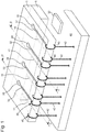
- la
figure 1 est une vue de dessus en perspective d'un dispositif d'affichage à cristal liquide muni de touches tactiles selon l'invention ; - la
figure 2 est une vue en coupe selon la ligne II-II de lafigure 1 qui illustre la connexion électrique entre une broche de connexion et une première piste électriquement conductrice pour relier une première électrode structurée sur une face inférieure du substrat avant avec un dispositif extérieur de commande, et - la
figure 3 est une vue en coupe selon la ligne III-III de lafigure 1 qui illustre la connexion électrique entre une broche de connexion et une troisième piste électriquement conductrice pour relier une troisième électrode structurée sur une face supérieure du substrat avant avec le dispositif extérieur de commande.
- the
figure 1 is a perspective top view of a liquid crystal display device provided with tactile keys according to the invention; - the
figure 2 is a sectional view along line II-II of thefigure 1 illustrating the electrical connection between a connecting pin and a first electrically conductive track for connecting a first structured electrode on a lower face of the front substrate with an external control device, and - the
figure 3 is a sectional view along line III-III of thefigure 1 which illustrates the electrical connection between a connecting pin and a third electrically conductive track for connecting a third electrode structured on an upper face of the front substrate with the external control device.
La présente invention procède de l'idée générale inventive qui consiste à structurer sur un même substrat transparent d'un côté une ou plusieurs électrodes nécessaires pour commander les propriétés optiques d'un cristal liquide, et de l'autre côté une ou plusieurs électrodes qui forment autant de touches tactiles capacitives permettant à un utilisateur d'introduire des commandes dans un dispositif de commande extérieur au dispositif d'affichage à cristal liquide selon l'invention. Grâce à ces caractéristiques, la présente invention permet de réaliser un dispositif capable à la fois d'afficher des informations et de prendre en compte des instructions d'un utilisateur en un nombre limité d'étapes de fabrication, à l'aide d'un même matériau et sur un même élément. Les économies en termes de coûts de fabrication et de composants nécessaires à la fabrication sont sensibles. D'autre part, il suffit d'enfoncer les broches de connexion dans des trous correspondants pratiqués dans une carte à circuits imprimés pour pouvoir relier le dispositif d'affichage à cristal liquide selon l'invention à un dispositif extérieur de commande. Les opérations de raccordement électrique du dispositif d'affichage à cristal liquide selon l'invention sont donc réduites au maximum, ce qui permet également de réaliser des économies sur le temps de fabrication.The present invention proceeds from the general inventive idea of structuring on the same transparent substrate on one side one or more electrodes necessary to control the optical properties of a liquid crystal, and on the other side one or more electrodes which form as capacitive touch keys allowing a user to introduce commands into a control device outside the liquid crystal display device according to the invention. Thanks to these features, the present invention makes it possible to produce a device able to both display information and to take into account instructions of a user in a limited number of manufacturing steps, using the same material and on the same element. Savings in manufacturing costs and components required for manufacturing are sensitive. On the other hand, it is sufficient to push the connection pins into corresponding holes in a printed circuit board to be able to connect the liquid crystal display device according to the invention to an external control device. The electrical connection operations of the liquid crystal display device according to the invention are therefore reduced to the maximum, which also allows savings on the manufacturing time.
L'invention sera décrite pour partie en liaison avec les
Les premières électrodes 12 sont prolongées vers l'extérieur du dispositif d'affichage à cristal liquide 1 par des premières pistes conductrices 20 qui sont structurées sur la face inférieure 14 du substrat avant 2. Les deuxièmes électrodes 16 qui sont structurées sur la face supérieure 18 du substrat arrière 6 sont renvoyées vers la face inférieure 14 du substrat avant 2 et sont prolongées vers l'extérieur du dispositif d'affichage à cristal liquide 1 par des deuxièmes pistes conductrices 24. De préférence, ces premières et deuxièmes pistes conductrices 20, 24 sont réalisées au moyen du même matériau et des mêmes techniques de gravure que les premières et deuxièmes électrodes 12, 16. Ces premières et deuxièmes pistes conductrices 20, 24 s'étendent à proximité du bord ou jusqu'au bord du substrat avant 2.The
Une pluralité de troisièmes électrodes 26 qui définissent des zones tactiles capacitives sont structurées sur une face supérieure 28 du substrat avant 2. Ces troisièmes électrodes 26 sont réalisées en un matériau transparent électriquement conducteur qui est, de préférence, le même que celui utilisé pour réaliser les premières et deuxièmes électrodes 12, 16. De préférence, ces troisièmes électrodes 26 sont réalisées par les mêmes techniques de fabrication que celles utilisées pour les premières et deuxièmes électrodes 12, 16. Ces troisièmes électrodes 26 définissent des zones de contact dont la capacité change lorsque l'utilisateur pose un doigt dessus, ce qui permet d'envoyer un signal de commande à un dispositif extérieur de commande 30. Ces troisièmes électrodes 26 sont prolongées vers le bord du substrat avant 2 par des troisièmes pistes conductrices 32 qui sont structurées en même temps que les troisièmes électrodes 26.A plurality of
A titre d'exemple purement illustratif et nullement limitatif, le cristal liquide utilisé dans le dispositif d'affichage à cristal liquide 1 selon l'invention est du type nématique en hélice, également bien connu sous sa dénomination anglo-saxonne Twisted Nematic liquid crystal ou cristal liquide TN. Ceci implique que le dispositif d'affichage à cristal liquide 1 soit muni d'un polariseur avant 34 solidarisé sur la face supérieure 28 du substrat avant 2 et recouvrant les troisièmes électrodes 26, ainsi que d'au moins un polariseur arrière 36 solidarisé sur une face inférieure 38 du substrat arrière 6. Selon qu'un contraste d'affichage positif ou négatif est recherché, les directions de polarisation du polariseur avant 34 et du polariseur arrière 36 sont croisées ou parallèles l'une par rapport à l'autre. A titre de variante, il est possible de remplacer le polariseur arrière 36 par un réflecteur, c'est-à-dire un polariseur muni d'une couche réfléchissante sur sa face arrière, ou bien par un transflecteur, c'est-à-dire un polariseur associé à une couche réflective semi-transparente.By way of purely illustrative and in no way limiting example, the liquid crystal used in the liquid
Un examen de la
De même, un examen de la
Il va de soi que la présente invention n'est pas limitée au mode de réalisation qui vient d'être décrit et que diverses modifications et variantes simples peuvent être envisagées par l'homme du métier sans sortir du cadre de l'invention tel que défini par les revendications annexées. En particulier, la présente invention a été décrite en liaison avec un dispositif d'affichage à cristal liquide 1 comprenant plusieurs premières, deuxièmes et troisièmes électrodes 12, 16 et 26. Il va cependant de soi que dans son acception la plus simple, le dispositif d'affichage à cristal liquide 1 peut ne comprendre qu'une première et une deuxième électrode 12, 16 pour modifier, par application d'une tension électrique au point de croisement de ces deux électrodes 12 et 26, les propriétés optiques du cristal liquide, et une seule troisième électrode 26 pour définir une unique zone de contact.It goes without saying that the present invention is not limited to the embodiment which has just been described and that various modifications and variants simple can be envisaged by the skilled person without departing from the scope of the invention as defined by the appended claims. In particular, the present invention has been described in connection with a liquid
De même, la présente invention a été décrite en liaison avec un dispositif d'affichage à cristal liquide 1 comprenant un cristal liquide du type nématique en hélice, également bien connu sous sa dénomination anglosaxonne Twisted Nematic liquid crystal ou cristal liquide TN. Il va cependant de soi que d'autres cristaux liquides tels que super-nématique en hélice (Super Twisted Nematic ou STN) ou du type hôte-invité (guest-host liquid crystal) peuvent être envisagés. Dans le cas d'un cristal liquide du type guest-host, on peut s'affranchir de tout polariseur.Similarly, the present invention has been described in connection with a liquid
De même, dans la description ci-dessus, il a été envisagé le cas où les premières et les deuxièmes électrodes 12, 16 qui permettent de modifier les propriétés optiques du cristal liquide, et les troisièmes électrodes 26 qui permettent à l'utilisateur d'introduire des données sont toutes reliées à un même dispositif extérieur de commande 30. Il est cependant toutefois possible d'envisager que les électrodes permettant de contrôler le cristal liquide d'une part, et les électrodes tactiles capacitives d'autre part soient reliées à deux dispositifs extérieurs de commande distincts.Similarly, in the above description, it has been envisaged the case where the first and the
Il est également envisageable que seules les troisièmes électrodes 26 qui permettent à l'utilisateur d'introduire des données dans le dispositif extérieur de commande 30 soient connectées au moyen de broches de connexion 40, tandis que les premières et secondes électrodes 12, 16 qui permettent de contrôler les propriétés optiques du cristal liquide peuvent être reliées avec l'environnement extérieur par exemple au moyen d'un connecteur de type Zebra® formé d'une succession de feuilles isolantes par exemple en élastomère et de feuilles conductrices de l'électricité par exemple en cuivre.It is also conceivable that only the
- 1.1.
- Dispositif d'affichage à cristal liquideLiquid crystal display device
- 2.2.
- Substrat avantSubstrate before
- 4.4.
- ObservateurObserver
- 6.6.
- Substrat arrièreRear substrate
- 8.8.
- Cadre de scellementSealing frame
- 10.10.
- Enceinte étancheWaterproof enclosure
- 12.12.
- Premières électrodesFirst electrodes
- 14.14.
- Face inférieureLower side
- 16.16.
- Deuxièmes électrodesSecond electrodes
- 18.18.
- Face supérieureUpper side
- 20.20.
- Premières pistes conductricesFirst conductive tracks
- 24.24.
- Deuxièmes pistes conductricesSecond conductive tracks
- 26.26.
- Troisièmes électrodesThird electrodes
- 28.28.
- Face supérieureUpper side
- 30.30.
- Dispositif extérieur de commandeExternal control device
- 32.32.
- Troisièmes pistes conductricesThird conductive tracks
- 34.34.
- Polariseur avantFront polarizer
- 36.36.
- Polariseur arrièreRear polarizer
- 38.38.
- Face inférieureLower side
- 40.40.
- Broche de connexionConnection pin
- 42.42.
- Tigestem
- 44.44.
- Carte à circuits imprimésPrinted circuit board
- 46.46.
- TêteHead
- 48.48.
- BrasArms
Claims (2)
Priority Applications (1)
| Application Number | Priority Date | Filing Date | Title |
|---|---|---|---|
| EP16202831.0A EP3333620B1 (en) | 2016-12-08 | 2016-12-08 | Display device provided with touch keys |
Applications Claiming Priority (1)
| Application Number | Priority Date | Filing Date | Title |
|---|---|---|---|
| EP16202831.0A EP3333620B1 (en) | 2016-12-08 | 2016-12-08 | Display device provided with touch keys |
Publications (2)
| Publication Number | Publication Date |
|---|---|
| EP3333620A1 true EP3333620A1 (en) | 2018-06-13 |
| EP3333620B1 EP3333620B1 (en) | 2019-01-30 |
Family
ID=57539072
Family Applications (1)
| Application Number | Title | Priority Date | Filing Date |
|---|---|---|---|
| EP16202831.0A Active EP3333620B1 (en) | 2016-12-08 | 2016-12-08 | Display device provided with touch keys |
Country Status (1)
| Country | Link |
|---|---|
| EP (1) | EP3333620B1 (en) |
Citations (4)
| Publication number | Priority date | Publication date | Assignee | Title |
|---|---|---|---|---|
| JP2002169143A (en) * | 2000-11-30 | 2002-06-14 | Nippon Seiki Co Ltd | Liquid crystal display |
| JP2006267762A (en) * | 2005-03-25 | 2006-10-05 | Nippon Seiki Co Ltd | Liquid crystal display device |
| WO2013042646A1 (en) * | 2011-09-22 | 2013-03-28 | シャープ株式会社 | Image display device |
| US20150049257A1 (en) * | 2013-08-14 | 2015-02-19 | Hannstar Display Corporation | Touch display apparatus |
-
2016
- 2016-12-08 EP EP16202831.0A patent/EP3333620B1/en active Active
Patent Citations (4)
| Publication number | Priority date | Publication date | Assignee | Title |
|---|---|---|---|---|
| JP2002169143A (en) * | 2000-11-30 | 2002-06-14 | Nippon Seiki Co Ltd | Liquid crystal display |
| JP2006267762A (en) * | 2005-03-25 | 2006-10-05 | Nippon Seiki Co Ltd | Liquid crystal display device |
| WO2013042646A1 (en) * | 2011-09-22 | 2013-03-28 | シャープ株式会社 | Image display device |
| US20150049257A1 (en) * | 2013-08-14 | 2015-02-19 | Hannstar Display Corporation | Touch display apparatus |
Also Published As
| Publication number | Publication date |
|---|---|
| EP3333620B1 (en) | 2019-01-30 |
Similar Documents
| Publication | Publication Date | Title |
|---|---|---|
| EP3058447B1 (en) | Touch and hover sensing with conductive polarizer | |
| US10282012B2 (en) | Touch display panel with force sensor | |
| CN101223494B (en) | Flexible touch screen display | |
| EP3650957B1 (en) | Object provided with an electro-optical display device | |
| WO2016066282A1 (en) | Capacitive control interface device integrated with a display screen | |
| EP3006994B1 (en) | Display assembly including two stacked display devices | |
| FR2973921A1 (en) | DOUBLE MODE TOUCH MODE MODULE AND DOUBLE MODE TOUCH SCREEN | |
| EP2073108A1 (en) | Screen with capacitive tactile areas | |
| FR2952444A1 (en) | LIQUID CRYSTAL STEREOSCOPIC DISPLAY DEVICE COMPRISING A TOUCH SCREEN AND METHOD FOR MANUFACTURING THE SAME | |
| EP3007015B1 (en) | Hybrid display assembly including a solar cell | |
| US20150248173A1 (en) | Keycap Including a Liquid Crystal Panel and Polarizing Glyphs | |
| EP3650958B1 (en) | Object provided with an electro-optical display device | |
| KR102082479B1 (en) | Touch sensor and image display device including the same | |
| EP1734587B1 (en) | Fabrication method for a transparent device having transparent electrodes and such device | |
| JP6148361B2 (en) | Wristwatch including flange | |
| TW201246314A (en) | Input device and method of manufacturing the same | |
| EP3333620B1 (en) | Display device provided with touch keys | |
| US9983423B2 (en) | Touch sensitive display with graded index layer | |
| EP3229166B1 (en) | Detection of the opening of a data input device | |
| CH712577B1 (en) | Liquid crystal display device with touch keys. | |
| CN102971694B (en) | Window panel assembly and the one-piece type electrostatic capacitance contact panel of window panel | |
| WO2017108898A1 (en) | Control interface for automotive vehicle | |
| CH715286B1 (en) | Object fitted with an electro-optical display device. | |
| EP3069200B1 (en) | Electromechanical or digital watch comprising a dial and method for manufacturing such a dial | |
| CH715285B1 (en) | Object fitted with an electro-optical display device. |
Legal Events
| Date | Code | Title | Description |
|---|---|---|---|
| STAA | Information on the status of an ep patent application or granted ep patent |
Free format text: STATUS: EXAMINATION IS IN PROGRESS |
|
| PUAI | Public reference made under article 153(3) epc to a published international application that has entered the european phase |
Free format text: ORIGINAL CODE: 0009012 |
|
| 17P | Request for examination filed |
Effective date: 20170718 |
|
| AK | Designated contracting states |
Kind code of ref document: A1 Designated state(s): AL AT BE BG CH CY CZ DE DK EE ES FI FR GB GR HR HU IE IS IT LI LT LU LV MC MK MT NL NO PL PT RO RS SE SI SK SM TR |
|
| AX | Request for extension of the european patent |
Extension state: BA ME |
|
| GRAP | Despatch of communication of intention to grant a patent |
Free format text: ORIGINAL CODE: EPIDOSNIGR1 |
|
| STAA | Information on the status of an ep patent application or granted ep patent |
Free format text: STATUS: GRANT OF PATENT IS INTENDED |
|
| INTG | Intention to grant announced |
Effective date: 20180814 |
|
| GRAS | Grant fee paid |
Free format text: ORIGINAL CODE: EPIDOSNIGR3 |
|
| GRAJ | Information related to disapproval of communication of intention to grant by the applicant or resumption of examination proceedings by the epo deleted |
Free format text: ORIGINAL CODE: EPIDOSDIGR1 |
|
| GRAL | Information related to payment of fee for publishing/printing deleted |
Free format text: ORIGINAL CODE: EPIDOSDIGR3 |
|
| STAA | Information on the status of an ep patent application or granted ep patent |
Free format text: STATUS: EXAMINATION IS IN PROGRESS |
|
| GRAR | Information related to intention to grant a patent recorded |
Free format text: ORIGINAL CODE: EPIDOSNIGR71 |
|
| STAA | Information on the status of an ep patent application or granted ep patent |
Free format text: STATUS: GRANT OF PATENT IS INTENDED |
|
| INTC | Intention to grant announced (deleted) | ||
| INTG | Intention to grant announced |
Effective date: 20181030 |
|
| GRAA | (expected) grant |
Free format text: ORIGINAL CODE: 0009210 |
|
| STAA | Information on the status of an ep patent application or granted ep patent |
Free format text: STATUS: THE PATENT HAS BEEN GRANTED |
|
| AK | Designated contracting states |
Kind code of ref document: B1 Designated state(s): AL AT BE BG CH CY CZ DE DK EE ES FI FR GB GR HR HU IE IS IT LI LT LU LV MC MK MT NL NO PL PT RO RS SE SI SK SM TR |
|
| REG | Reference to a national code |
Ref country code: GB Ref legal event code: FG4D Free format text: NOT ENGLISH |
|
| REG | Reference to a national code |
Ref country code: CH Ref legal event code: EP |
|
| REG | Reference to a national code |
Ref country code: CH Ref legal event code: NV Representative=s name: ICB INGENIEURS CONSEILS EN BREVETS SA, CH Ref country code: AT Ref legal event code: REF Ref document number: 1093730 Country of ref document: AT Kind code of ref document: T Effective date: 20190215 |
|
| REG | Reference to a national code |
Ref country code: IE Ref legal event code: FG4D Free format text: LANGUAGE OF EP DOCUMENT: FRENCH |
|
| REG | Reference to a national code |
Ref country code: DE Ref legal event code: R096 Ref document number: 602016009628 Country of ref document: DE |
|
| REG | Reference to a national code |
Ref country code: LT Ref legal event code: MG4D |
|
| REG | Reference to a national code |
Ref country code: NL Ref legal event code: MP Effective date: 20190130 |
|
| PG25 | Lapsed in a contracting state [announced via postgrant information from national office to epo] |
Ref country code: LT Free format text: LAPSE BECAUSE OF FAILURE TO SUBMIT A TRANSLATION OF THE DESCRIPTION OR TO PAY THE FEE WITHIN THE PRESCRIBED TIME-LIMIT Effective date: 20190130 Ref country code: PL Free format text: LAPSE BECAUSE OF FAILURE TO SUBMIT A TRANSLATION OF THE DESCRIPTION OR TO PAY THE FEE WITHIN THE PRESCRIBED TIME-LIMIT Effective date: 20190130 Ref country code: NL Free format text: LAPSE BECAUSE OF FAILURE TO SUBMIT A TRANSLATION OF THE DESCRIPTION OR TO PAY THE FEE WITHIN THE PRESCRIBED TIME-LIMIT Effective date: 20190130 Ref country code: ES Free format text: LAPSE BECAUSE OF FAILURE TO SUBMIT A TRANSLATION OF THE DESCRIPTION OR TO PAY THE FEE WITHIN THE PRESCRIBED TIME-LIMIT Effective date: 20190130 Ref country code: SE Free format text: LAPSE BECAUSE OF FAILURE TO SUBMIT A TRANSLATION OF THE DESCRIPTION OR TO PAY THE FEE WITHIN THE PRESCRIBED TIME-LIMIT Effective date: 20190130 Ref country code: FI Free format text: LAPSE BECAUSE OF FAILURE TO SUBMIT A TRANSLATION OF THE DESCRIPTION OR TO PAY THE FEE WITHIN THE PRESCRIBED TIME-LIMIT Effective date: 20190130 Ref country code: NO Free format text: LAPSE BECAUSE OF FAILURE TO SUBMIT A TRANSLATION OF THE DESCRIPTION OR TO PAY THE FEE WITHIN THE PRESCRIBED TIME-LIMIT Effective date: 20190430 Ref country code: PT Free format text: LAPSE BECAUSE OF FAILURE TO SUBMIT A TRANSLATION OF THE DESCRIPTION OR TO PAY THE FEE WITHIN THE PRESCRIBED TIME-LIMIT Effective date: 20190530 |
|
| REG | Reference to a national code |
Ref country code: AT Ref legal event code: MK05 Ref document number: 1093730 Country of ref document: AT Kind code of ref document: T Effective date: 20190130 |
|
| PG25 | Lapsed in a contracting state [announced via postgrant information from national office to epo] |
Ref country code: GR Free format text: LAPSE BECAUSE OF FAILURE TO SUBMIT A TRANSLATION OF THE DESCRIPTION OR TO PAY THE FEE WITHIN THE PRESCRIBED TIME-LIMIT Effective date: 20190501 Ref country code: IS Free format text: LAPSE BECAUSE OF FAILURE TO SUBMIT A TRANSLATION OF THE DESCRIPTION OR TO PAY THE FEE WITHIN THE PRESCRIBED TIME-LIMIT Effective date: 20190530 Ref country code: RS Free format text: LAPSE BECAUSE OF FAILURE TO SUBMIT A TRANSLATION OF THE DESCRIPTION OR TO PAY THE FEE WITHIN THE PRESCRIBED TIME-LIMIT Effective date: 20190130 Ref country code: LV Free format text: LAPSE BECAUSE OF FAILURE TO SUBMIT A TRANSLATION OF THE DESCRIPTION OR TO PAY THE FEE WITHIN THE PRESCRIBED TIME-LIMIT Effective date: 20190130 Ref country code: BG Free format text: LAPSE BECAUSE OF FAILURE TO SUBMIT A TRANSLATION OF THE DESCRIPTION OR TO PAY THE FEE WITHIN THE PRESCRIBED TIME-LIMIT Effective date: 20190430 Ref country code: HR Free format text: LAPSE BECAUSE OF FAILURE TO SUBMIT A TRANSLATION OF THE DESCRIPTION OR TO PAY THE FEE WITHIN THE PRESCRIBED TIME-LIMIT Effective date: 20190130 |
|
| PG25 | Lapsed in a contracting state [announced via postgrant information from national office to epo] |
Ref country code: AL Free format text: LAPSE BECAUSE OF FAILURE TO SUBMIT A TRANSLATION OF THE DESCRIPTION OR TO PAY THE FEE WITHIN THE PRESCRIBED TIME-LIMIT Effective date: 20190130 Ref country code: SK Free format text: LAPSE BECAUSE OF FAILURE TO SUBMIT A TRANSLATION OF THE DESCRIPTION OR TO PAY THE FEE WITHIN THE PRESCRIBED TIME-LIMIT Effective date: 20190130 Ref country code: CZ Free format text: LAPSE BECAUSE OF FAILURE TO SUBMIT A TRANSLATION OF THE DESCRIPTION OR TO PAY THE FEE WITHIN THE PRESCRIBED TIME-LIMIT Effective date: 20190130 Ref country code: RO Free format text: LAPSE BECAUSE OF FAILURE TO SUBMIT A TRANSLATION OF THE DESCRIPTION OR TO PAY THE FEE WITHIN THE PRESCRIBED TIME-LIMIT Effective date: 20190130 Ref country code: EE Free format text: LAPSE BECAUSE OF FAILURE TO SUBMIT A TRANSLATION OF THE DESCRIPTION OR TO PAY THE FEE WITHIN THE PRESCRIBED TIME-LIMIT Effective date: 20190130 Ref country code: DK Free format text: LAPSE BECAUSE OF FAILURE TO SUBMIT A TRANSLATION OF THE DESCRIPTION OR TO PAY THE FEE WITHIN THE PRESCRIBED TIME-LIMIT Effective date: 20190130 Ref country code: IT Free format text: LAPSE BECAUSE OF FAILURE TO SUBMIT A TRANSLATION OF THE DESCRIPTION OR TO PAY THE FEE WITHIN THE PRESCRIBED TIME-LIMIT Effective date: 20190130 |
|
| REG | Reference to a national code |
Ref country code: DE Ref legal event code: R097 Ref document number: 602016009628 Country of ref document: DE |
|
| PG25 | Lapsed in a contracting state [announced via postgrant information from national office to epo] |
Ref country code: SM Free format text: LAPSE BECAUSE OF FAILURE TO SUBMIT A TRANSLATION OF THE DESCRIPTION OR TO PAY THE FEE WITHIN THE PRESCRIBED TIME-LIMIT Effective date: 20190130 |
|
| PLBE | No opposition filed within time limit |
Free format text: ORIGINAL CODE: 0009261 |
|
| STAA | Information on the status of an ep patent application or granted ep patent |
Free format text: STATUS: NO OPPOSITION FILED WITHIN TIME LIMIT |
|
| PG25 | Lapsed in a contracting state [announced via postgrant information from national office to epo] |
Ref country code: AT Free format text: LAPSE BECAUSE OF FAILURE TO SUBMIT A TRANSLATION OF THE DESCRIPTION OR TO PAY THE FEE WITHIN THE PRESCRIBED TIME-LIMIT Effective date: 20190130 |
|
| 26N | No opposition filed |
Effective date: 20191031 |
|
| PG25 | Lapsed in a contracting state [announced via postgrant information from national office to epo] |
Ref country code: TR Free format text: LAPSE BECAUSE OF FAILURE TO SUBMIT A TRANSLATION OF THE DESCRIPTION OR TO PAY THE FEE WITHIN THE PRESCRIBED TIME-LIMIT Effective date: 20190130 |
|
| REG | Reference to a national code |
Ref country code: BE Ref legal event code: MM Effective date: 20191231 |
|
| PG25 | Lapsed in a contracting state [announced via postgrant information from national office to epo] |
Ref country code: MC Free format text: LAPSE BECAUSE OF FAILURE TO SUBMIT A TRANSLATION OF THE DESCRIPTION OR TO PAY THE FEE WITHIN THE PRESCRIBED TIME-LIMIT Effective date: 20190130 |
|
| PG25 | Lapsed in a contracting state [announced via postgrant information from national office to epo] |
Ref country code: LU Free format text: LAPSE BECAUSE OF NON-PAYMENT OF DUE FEES Effective date: 20191208 Ref country code: IE Free format text: LAPSE BECAUSE OF NON-PAYMENT OF DUE FEES Effective date: 20191208 |
|
| PG25 | Lapsed in a contracting state [announced via postgrant information from national office to epo] |
Ref country code: BE Free format text: LAPSE BECAUSE OF NON-PAYMENT OF DUE FEES Effective date: 20191231 |
|
| PG25 | Lapsed in a contracting state [announced via postgrant information from national office to epo] |
Ref country code: CY Free format text: LAPSE BECAUSE OF FAILURE TO SUBMIT A TRANSLATION OF THE DESCRIPTION OR TO PAY THE FEE WITHIN THE PRESCRIBED TIME-LIMIT Effective date: 20190130 |
|
| PG25 | Lapsed in a contracting state [announced via postgrant information from national office to epo] |
Ref country code: HU Free format text: LAPSE BECAUSE OF FAILURE TO SUBMIT A TRANSLATION OF THE DESCRIPTION OR TO PAY THE FEE WITHIN THE PRESCRIBED TIME-LIMIT; INVALID AB INITIO Effective date: 20161208 Ref country code: MT Free format text: LAPSE BECAUSE OF FAILURE TO SUBMIT A TRANSLATION OF THE DESCRIPTION OR TO PAY THE FEE WITHIN THE PRESCRIBED TIME-LIMIT Effective date: 20190130 |
|
| GBPC | Gb: european patent ceased through non-payment of renewal fee |
Effective date: 20201208 |
|
| PG25 | Lapsed in a contracting state [announced via postgrant information from national office to epo] |
Ref country code: SI Free format text: LAPSE BECAUSE OF FAILURE TO SUBMIT A TRANSLATION OF THE DESCRIPTION OR TO PAY THE FEE WITHIN THE PRESCRIBED TIME-LIMIT Effective date: 20190130 |
|
| PG25 | Lapsed in a contracting state [announced via postgrant information from national office to epo] |
Ref country code: GB Free format text: LAPSE BECAUSE OF NON-PAYMENT OF DUE FEES Effective date: 20201208 |
|
| PG25 | Lapsed in a contracting state [announced via postgrant information from national office to epo] |
Ref country code: MK Free format text: LAPSE BECAUSE OF FAILURE TO SUBMIT A TRANSLATION OF THE DESCRIPTION OR TO PAY THE FEE WITHIN THE PRESCRIBED TIME-LIMIT Effective date: 20190130 |
|
| PGFP | Annual fee paid to national office [announced via postgrant information from national office to epo] |
Ref country code: CH Payment date: 20230101 Year of fee payment: 7 |
|
| P01 | Opt-out of the competence of the unified patent court (upc) registered |
Effective date: 20230611 |
|
| PGFP | Annual fee paid to national office [announced via postgrant information from national office to epo] |
Ref country code: FR Payment date: 20231122 Year of fee payment: 8 Ref country code: DE Payment date: 20231121 Year of fee payment: 8 |
|
| PGFP | Annual fee paid to national office [announced via postgrant information from national office to epo] |
Ref country code: CH Payment date: 20240101 Year of fee payment: 8 |