EP3333620A1 - Anzeigevorrichtung mit berührungsempfindlichen tasten - Google Patents
Anzeigevorrichtung mit berührungsempfindlichen tasten Download PDFInfo
- Publication number
- EP3333620A1 EP3333620A1 EP16202831.0A EP16202831A EP3333620A1 EP 3333620 A1 EP3333620 A1 EP 3333620A1 EP 16202831 A EP16202831 A EP 16202831A EP 3333620 A1 EP3333620 A1 EP 3333620A1
- Authority
- EP
- European Patent Office
- Prior art keywords
- electrode
- liquid crystal
- front substrate
- structured
- electrically conductive
- Prior art date
- Legal status (The legal status is an assumption and is not a legal conclusion. Google has not performed a legal analysis and makes no representation as to the accuracy of the status listed.)
- Granted
Links
Images

Classifications
-
- G—PHYSICS
- G02—OPTICS
- G02F—OPTICAL DEVICES OR ARRANGEMENTS FOR THE CONTROL OF LIGHT BY MODIFICATION OF THE OPTICAL PROPERTIES OF THE MEDIA OF THE ELEMENTS INVOLVED THEREIN; NON-LINEAR OPTICS; FREQUENCY-CHANGING OF LIGHT; OPTICAL LOGIC ELEMENTS; OPTICAL ANALOGUE/DIGITAL CONVERTERS
- G02F1/00—Devices or arrangements for the control of the intensity, colour, phase, polarisation or direction of light arriving from an independent light source, e.g. switching, gating or modulating; Non-linear optics
- G02F1/01—Devices or arrangements for the control of the intensity, colour, phase, polarisation or direction of light arriving from an independent light source, e.g. switching, gating or modulating; Non-linear optics for the control of the intensity, phase, polarisation or colour
- G02F1/13—Devices or arrangements for the control of the intensity, colour, phase, polarisation or direction of light arriving from an independent light source, e.g. switching, gating or modulating; Non-linear optics for the control of the intensity, phase, polarisation or colour based on liquid crystals, e.g. single liquid crystal display cells
- G02F1/133—Constructional arrangements; Operation of liquid crystal cells; Circuit arrangements
- G02F1/1333—Constructional arrangements; Manufacturing methods
- G02F1/13338—Input devices, e.g. touch panels
-
- G—PHYSICS
- G02—OPTICS
- G02F—OPTICAL DEVICES OR ARRANGEMENTS FOR THE CONTROL OF LIGHT BY MODIFICATION OF THE OPTICAL PROPERTIES OF THE MEDIA OF THE ELEMENTS INVOLVED THEREIN; NON-LINEAR OPTICS; FREQUENCY-CHANGING OF LIGHT; OPTICAL LOGIC ELEMENTS; OPTICAL ANALOGUE/DIGITAL CONVERTERS
- G02F1/00—Devices or arrangements for the control of the intensity, colour, phase, polarisation or direction of light arriving from an independent light source, e.g. switching, gating or modulating; Non-linear optics
- G02F1/01—Devices or arrangements for the control of the intensity, colour, phase, polarisation or direction of light arriving from an independent light source, e.g. switching, gating or modulating; Non-linear optics for the control of the intensity, phase, polarisation or colour
- G02F1/13—Devices or arrangements for the control of the intensity, colour, phase, polarisation or direction of light arriving from an independent light source, e.g. switching, gating or modulating; Non-linear optics for the control of the intensity, phase, polarisation or colour based on liquid crystals, e.g. single liquid crystal display cells
- G02F1/133—Constructional arrangements; Operation of liquid crystal cells; Circuit arrangements
- G02F1/1333—Constructional arrangements; Manufacturing methods
- G02F1/1345—Conductors connecting electrodes to cell terminals
- G02F1/13452—Conductors connecting driver circuitry and terminals of panels
-
- G—PHYSICS
- G06—COMPUTING OR CALCULATING; COUNTING
- G06F—ELECTRIC DIGITAL DATA PROCESSING
- G06F3/00—Input arrangements for transferring data to be processed into a form capable of being handled by the computer; Output arrangements for transferring data from processing unit to output unit, e.g. interface arrangements
- G06F3/01—Input arrangements or combined input and output arrangements for interaction between user and computer
- G06F3/03—Arrangements for converting the position or the displacement of a member into a coded form
- G06F3/041—Digitisers, e.g. for touch screens or touch pads, characterised by the transducing means
- G06F3/0412—Digitisers structurally integrated in a display
-
- G—PHYSICS
- G06—COMPUTING OR CALCULATING; COUNTING
- G06F—ELECTRIC DIGITAL DATA PROCESSING
- G06F3/00—Input arrangements for transferring data to be processed into a form capable of being handled by the computer; Output arrangements for transferring data from processing unit to output unit, e.g. interface arrangements
- G06F3/01—Input arrangements or combined input and output arrangements for interaction between user and computer
- G06F3/03—Arrangements for converting the position or the displacement of a member into a coded form
- G06F3/041—Digitisers, e.g. for touch screens or touch pads, characterised by the transducing means
- G06F3/0416—Control or interface arrangements specially adapted for digitisers
- G06F3/04164—Connections between sensors and controllers, e.g. routing lines between electrodes and connection pads
-
- G—PHYSICS
- G06—COMPUTING OR CALCULATING; COUNTING
- G06F—ELECTRIC DIGITAL DATA PROCESSING
- G06F3/00—Input arrangements for transferring data to be processed into a form capable of being handled by the computer; Output arrangements for transferring data from processing unit to output unit, e.g. interface arrangements
- G06F3/01—Input arrangements or combined input and output arrangements for interaction between user and computer
- G06F3/03—Arrangements for converting the position or the displacement of a member into a coded form
- G06F3/041—Digitisers, e.g. for touch screens or touch pads, characterised by the transducing means
- G06F3/044—Digitisers, e.g. for touch screens or touch pads, characterised by the transducing means by capacitive means
- G06F3/0443—Digitisers, e.g. for touch screens or touch pads, characterised by the transducing means by capacitive means using a single layer of sensing electrodes
Definitions
- the present invention relates to a display device with touch keys.
- the present invention particularly relates to a display device of the liquid crystal type comprising such tactile keys.
- a liquid crystal display cell comprises a front substrate oriented on the observer side and a rear substrate that extends parallel to and away from the front substrate.
- the front and rear substrates are joined together by means of a sealing frame which delimits a sealed enclosure for the confinement of a liquid crystal.
- a lower surface of the front substrate carries at least one electrode and an upper surface of the rear substrate carries at least one corresponding counter electrode.
- Such a data input device typically comprises a flexible or rigid film on a lower surface of which are structured touch control keys which are made by means of a conductive material such as tin-indium oxide, also known by its Anglo-Saxon name Indium-Tin Oxide or ITO.
- a conductive material such as tin-indium oxide, also known by its Anglo-Saxon name Indium-Tin Oxide or ITO.
- the touch-sensitive data input device is typically laminated to the upper surface of the front substrate of the liquid crystal display device.
- the touch-sensitive control device which requires, on the one hand, a flexible or rigid film on which the tactile control keys are structured, and on the other hand a flexible connection cable, is expensive.
- the present invention aims to overcome the drawbacks mentioned above as well as others by providing a liquid crystal display device with touch keys whose cost is substantially lowered.
- the present invention relates to a liquid crystal display device comprising a front substrate and a rear substrate which extends parallel to and away from the front substrate, the front and rear substrates being joined together by means of a sealing frame which delimits a sealed enclosure for the confinement of a liquid crystal, at least a first electrode being structured on a lower face of the front substrate, and at least a second opposite electrode being structured on an upper face of the rear substrate, the optical properties of the liquid crystal being modified by applying an appropriate electrical voltage to the point of intersection of the first and second electrodes in question, the at least one first electrode and the at least one second electrode being made of an electrically transparent material conductor and being extended outward of the display device liquid crystal gap by a first, respectively a second electrically conductive tracks structured on the lower face of the front substrate, at least a third electrode defining a capacitive touch zone being structured on an upper face of the front substrate, this third electrode being made in one transparent electrically conductive material and being extended by a third electrically conductive track with which a connection
- first and second connection pins in electrical contact with the first, respectively the second electrically conductive track make it possible to connect the first and the second electrode to the same external control device as the third electrode or to a separate external control device.
- the present invention provides a liquid crystal display device with capacitive touch keys that can be manufactured in a reduced number of steps and the cost is very advantageous.
- the first electrodes which, in cooperation with the second electrodes, make it possible to modify the optical properties of the liquid crystal of the display device, and the third electrodes which define the tactile keys are all structured on the front substrate, respectively on the lower face and on the upper face of the latter. Therefore, all of these electrodes can be made using the same manufacturing techniques such as photolithography, and preferably using the same electrically conductive material. It is understood that such rationalization of the production operations of the liquid crystal display device according to the invention saves time and achieve economies of scale which have a positive impact on the final cost of this device. display. In particular, it is not necessary to separately manufacture a device for inputting control data with tactile keys, which makes it possible to economize the flexible or rigid film on which the electrodes and the flexible connection cable were structured. associated.
- the liquid crystal display device according to the invention can be very easily connected to an external control device by simply pushing the pins into corresponding holes in a circuit card.
- printed also known as Anglo-Saxon Printed Circuit Board or PCB.
- the present invention proceeds from the general inventive idea of structuring on the same transparent substrate on one side one or more electrodes necessary to control the optical properties of a liquid crystal, and on the other side one or more electrodes which form as capacitive touch keys allowing a user to introduce commands into a control device outside the liquid crystal display device according to the invention. Thanks to these features, the present invention makes it possible to produce a device able to both display information and to take into account instructions of a user in a limited number of manufacturing steps, using the same material and on the same element. Savings in manufacturing costs and components required for manufacturing are sensitive. On the other hand, it is sufficient to push the connection pins into corresponding holes in a printed circuit board to be able to connect the liquid crystal display device according to the invention to an external control device. The electrical connection operations of the liquid crystal display device according to the invention are therefore reduced to the maximum, which also allows savings on the manufacturing time.
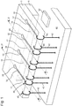
- the front substrate 2 and the rear substrate 6 are joined to each other by means of a sealing frame 8 which delimits a sealed enclosure 10 for the confinement of a liquid crystal.
- a plurality of first electrodes 12 is structured on a lower face 14 of the front substrate 2
- a plurality of second electrodes 16 is structured on an upper face 18 of the rear substrate 6.
- These first and second electrodes 12 and 16 are made of a material transparent conductor of electricity, for example tin-indium oxide, by means of etching techniques such as photolithography, and control the optical properties of the liquid crystal contained in the sealed enclosure 10.
- the first electrodes 12 are extended towards the outside of the liquid crystal display device 1 by first conductive tracks 20 which are structured on the underside 14 of the substrate before 2.
- the second electrodes 16 which are structured on the upper face 18 of the rear substrate 6 are returned to the lower face 14 of the front substrate 2 and are extended towards the outside of the liquid crystal display device 1 by second tracks
- these first and second conductive tracks 20, 24 are made using the same material and the same etching techniques as the first and second electrodes 12, 16.
- These first and second conductive tracks 20, 24 extend near the edge or to the edge of the front substrate 2.
- a plurality of third electrodes 26 which define capacitive touch zones are structured on an upper face 28 of the front substrate 2.
- These third electrodes 26 are made of an electrically conductive transparent material which is preferably the same as that used to make the electrodes.
- these third electrodes 26 are made by the same manufacturing techniques as those used for the first and second electrodes 12, 16.
- These third electrodes 26 define contact zones whose capacitance changes when the user places a finger on it, which makes it possible to send a control signal to an external control device 30.
- These third electrodes 26 are extended towards the edge of the front substrate 2 by third conductive tracks 32 which are structured at the same time time as the third electrodes 26.
- the liquid crystal used in the liquid crystal display device 1 according to the invention is of the nematic helical type, also well known by its Anglo-Saxon name Twisted Nematic liquid crystal or TN liquid crystal.
- the liquid crystal display device 1 is provided with a front polarizer 34 secured to the upper face 28 of the front substrate 2 and covering the third electrodes 26, as well as at least one rear polarizer 36 secured to a lower face 38 of the rear substrate 6.
- a positive or negative display contrast is The polarization directions of the front polarizer 34 and the rear polarizer 36 are cross-referenced or parallel to one another.
- rear polarizer 36 it is possible to replace the rear polarizer 36 by a reflector, that is to say a polarizer provided with a reflective layer on its rear face, or by a transflector, that is to say say a polarizer associated with a semi-transparent reflective layer.
- a reflector that is to say a polarizer provided with a reflective layer on its rear face
- a transflector that is to say say a polarizer associated with a semi-transparent reflective layer.
- connection pin 40 it is possible to electrically connect the first (or second) electrode 12 or 16 corresponding to an external control device 30.
- This connection pin 40 consists of a rod 42 whose free end is intended to be driven into a a hole formed in a printed circuit board 44, and a head 46 comprising two arms 48 which enclose the edge of the front substrate 2 and which make electrical contact with the first (or second) conductive track 20 or 24.
- maintaining the connection pins 40 is provided by the elasticity of the arms 48 and can be reinforced by depositing an adhesive layer.
- a review of the figure 3 reveals that a third conductive track 32, structured on the upper face 28 of the front substrate 2, is flush with the upper edge of this front substrate 2. Thanks to the use of a connection pin 40, it is possible to electrically connect the third electrode 26 to which the third conductive track 32 is connected to the external control device 30.
- the rod 42 of this connection pin 40 is intended to be depressed by its free end into a hole in the printed circuit board 44, and its two arms 48 enclose the edge of the front substrate 2 and make electrical contact with the third conductive track 32.
- the present invention is not limited to the embodiment which has just been described and that various modifications and variants simple can be envisaged by the skilled person without departing from the scope of the invention as defined by the appended claims.
- the present invention has been described in connection with a liquid crystal display device 1 comprising several first, second and third electrodes 12, 16 and 26.
- the device liquid crystal display 1 may comprise only first and second electrodes 12, 16 for modifying, by application of an electrical voltage at the point of intersection of these two electrodes 12 and 26, the optical properties of the liquid crystal, and a single third electrode 26 to define a single contact zone.
- liquid crystal display device 1 comprising a helical nematic type liquid crystal, also well known by its Anglosaxon name Twisted Nematic liquid crystal or TN liquid crystal. It goes without saying, however, that other liquid crystals such as Super Twisted Nematic (STN) or guest-host liquid crystal may be considered. In the case of a liquid crystal of the guest-host type, it is possible to dispense with any polarizer.
- STN Super Twisted Nematic
- guest-host liquid crystal it is possible to dispense with any polarizer.
- the electrodes making it possible to control the liquid crystal on the one hand, and the capacitive touch electrodes on the other hand are connected to two electromagnetic fields. separate external control devices.
- connection pins 40 the third electrodes 26 which allow the user to input data into the external control device 30 are connected by means of connection pins 40, while the first and second electrodes 12, 16 which allow to control the optical properties of the liquid crystal may be connected with the external environment for example by means of a Zebra® type connector formed of a succession of insulating sheets for example of elastomer and electrically conductive sheets for example copper.
Landscapes
- Engineering & Computer Science (AREA)
- Physics & Mathematics (AREA)
- Theoretical Computer Science (AREA)
- General Engineering & Computer Science (AREA)
- General Physics & Mathematics (AREA)
- Nonlinear Science (AREA)
- Human Computer Interaction (AREA)
- Crystallography & Structural Chemistry (AREA)
- Optics & Photonics (AREA)
- Chemical & Material Sciences (AREA)
- Mathematical Physics (AREA)
- Computer Networks & Wireless Communication (AREA)
- Devices For Indicating Variable Information By Combining Individual Elements (AREA)
- Liquid Crystal (AREA)
Priority Applications (1)
| Application Number | Priority Date | Filing Date | Title |
|---|---|---|---|
| EP16202831.0A EP3333620B1 (de) | 2016-12-08 | 2016-12-08 | Anzeigevorrichtung mit berührungsempfindlichen tasten |
Applications Claiming Priority (1)
| Application Number | Priority Date | Filing Date | Title |
|---|---|---|---|
| EP16202831.0A EP3333620B1 (de) | 2016-12-08 | 2016-12-08 | Anzeigevorrichtung mit berührungsempfindlichen tasten |
Publications (2)
| Publication Number | Publication Date |
|---|---|
| EP3333620A1 true EP3333620A1 (de) | 2018-06-13 |
| EP3333620B1 EP3333620B1 (de) | 2019-01-30 |
Family
ID=57539072
Family Applications (1)
| Application Number | Title | Priority Date | Filing Date |
|---|---|---|---|
| EP16202831.0A Active EP3333620B1 (de) | 2016-12-08 | 2016-12-08 | Anzeigevorrichtung mit berührungsempfindlichen tasten |
Country Status (1)
| Country | Link |
|---|---|
| EP (1) | EP3333620B1 (de) |
Citations (4)
| Publication number | Priority date | Publication date | Assignee | Title |
|---|---|---|---|---|
| JP2002169143A (ja) * | 2000-11-30 | 2002-06-14 | Nippon Seiki Co Ltd | 液晶表示装置 |
| JP2006267762A (ja) * | 2005-03-25 | 2006-10-05 | Nippon Seiki Co Ltd | 液晶表示装置 |
| WO2013042646A1 (ja) * | 2011-09-22 | 2013-03-28 | シャープ株式会社 | 画像表示装置 |
| US20150049257A1 (en) * | 2013-08-14 | 2015-02-19 | Hannstar Display Corporation | Touch display apparatus |
-
2016
- 2016-12-08 EP EP16202831.0A patent/EP3333620B1/de active Active
Patent Citations (4)
| Publication number | Priority date | Publication date | Assignee | Title |
|---|---|---|---|---|
| JP2002169143A (ja) * | 2000-11-30 | 2002-06-14 | Nippon Seiki Co Ltd | 液晶表示装置 |
| JP2006267762A (ja) * | 2005-03-25 | 2006-10-05 | Nippon Seiki Co Ltd | 液晶表示装置 |
| WO2013042646A1 (ja) * | 2011-09-22 | 2013-03-28 | シャープ株式会社 | 画像表示装置 |
| US20150049257A1 (en) * | 2013-08-14 | 2015-02-19 | Hannstar Display Corporation | Touch display apparatus |
Also Published As
| Publication number | Publication date |
|---|---|
| EP3333620B1 (de) | 2019-01-30 |
Similar Documents
| Publication | Publication Date | Title |
|---|---|---|
| EP3650958B1 (de) | Gegenstand, der mit einer elektrooptischen anzeigevorrichtung ausgestattet ist | |
| EP3650957B1 (de) | Gegenstand, der mit einer elektrooptischen anzeigevorrichtung ausgestattet ist | |
| US9547395B2 (en) | Touch and hover sensing with conductive polarizer | |
| EP2073108B1 (de) | Touchscreen mit kapazitiven Berührungszonen | |
| US20180136773A1 (en) | Touch display panel with force sensor | |
| WO2016066282A1 (fr) | Dispositif d'interface de commande capacitif integre a un ecran d'affichage | |
| FR2973921A1 (fr) | Module tactile double mode et ecran tactile double mode | |
| EP3007015B1 (de) | Hybridanzeigeeinheit, die eine solarzelle umfasst | |
| KR102082479B1 (ko) | 터치 센서 및 이를 포함하는 화상 표시 장치 | |
| EP2616888B1 (de) | Uhr mit taktilen kapazitiven bereichen mit einem von einer elektrisch leitenden abdeckung verschlossenen batteriefach | |
| TW201246314A (en) | Input device and method of manufacturing the same | |
| EP3333620B1 (de) | Anzeigevorrichtung mit berührungsempfindlichen tasten | |
| JP6148361B2 (ja) | フランジを含む腕時計 | |
| WO2017108898A1 (fr) | Interface de commande pour véhicule autmobile | |
| CH712577B1 (fr) | Dispositif d'affichage à cristal liquide muni de touches tactiles. | |
| US9983423B2 (en) | Touch sensitive display with graded index layer | |
| EP3229166B1 (de) | Vorrichtung zum erkennen des öffnens eines eingabegerätes | |
| EP1734587B1 (de) | Herstellungsverfahren für ein transparentes Element mit transparenten Elektroden und entsprechendes Element | |
| CH715286B1 (fr) | Objet muni d'un dispositif d`affichage électrooptique. | |
| CH715285B1 (fr) | Objet muni d'un dispositif d'affichage électrooptique. | |
| EP3069200B1 (de) | Elektromechanische oder digitale armbanduhr, die ein zifferblatt umfasst, und herstellungsverfahren eines solchen zifferblatts | |
| KR20170080230A (ko) | 표시장치 및 그 제조방법 | |
| CH707796B1 (fr) | Montre comprenant un réhaut portant des moyens de connexion électrique. | |
| CH710226A2 (fr) | Ensemble d'affichage hybride comprenant une cellule solaire pour objet portable. | |
| HK40027992B (en) | Object provided with an electro-optic display device |
Legal Events
| Date | Code | Title | Description |
|---|---|---|---|
| STAA | Information on the status of an ep patent application or granted ep patent |
Free format text: STATUS: EXAMINATION IS IN PROGRESS |
|
| PUAI | Public reference made under article 153(3) epc to a published international application that has entered the european phase |
Free format text: ORIGINAL CODE: 0009012 |
|
| 17P | Request for examination filed |
Effective date: 20170718 |
|
| AK | Designated contracting states |
Kind code of ref document: A1 Designated state(s): AL AT BE BG CH CY CZ DE DK EE ES FI FR GB GR HR HU IE IS IT LI LT LU LV MC MK MT NL NO PL PT RO RS SE SI SK SM TR |
|
| AX | Request for extension of the european patent |
Extension state: BA ME |
|
| GRAP | Despatch of communication of intention to grant a patent |
Free format text: ORIGINAL CODE: EPIDOSNIGR1 |
|
| STAA | Information on the status of an ep patent application or granted ep patent |
Free format text: STATUS: GRANT OF PATENT IS INTENDED |
|
| INTG | Intention to grant announced |
Effective date: 20180814 |
|
| GRAS | Grant fee paid |
Free format text: ORIGINAL CODE: EPIDOSNIGR3 |
|
| GRAJ | Information related to disapproval of communication of intention to grant by the applicant or resumption of examination proceedings by the epo deleted |
Free format text: ORIGINAL CODE: EPIDOSDIGR1 |
|
| GRAL | Information related to payment of fee for publishing/printing deleted |
Free format text: ORIGINAL CODE: EPIDOSDIGR3 |
|
| STAA | Information on the status of an ep patent application or granted ep patent |
Free format text: STATUS: EXAMINATION IS IN PROGRESS |
|
| GRAR | Information related to intention to grant a patent recorded |
Free format text: ORIGINAL CODE: EPIDOSNIGR71 |
|
| STAA | Information on the status of an ep patent application or granted ep patent |
Free format text: STATUS: GRANT OF PATENT IS INTENDED |
|
| INTC | Intention to grant announced (deleted) | ||
| INTG | Intention to grant announced |
Effective date: 20181030 |
|
| GRAA | (expected) grant |
Free format text: ORIGINAL CODE: 0009210 |
|
| STAA | Information on the status of an ep patent application or granted ep patent |
Free format text: STATUS: THE PATENT HAS BEEN GRANTED |
|
| AK | Designated contracting states |
Kind code of ref document: B1 Designated state(s): AL AT BE BG CH CY CZ DE DK EE ES FI FR GB GR HR HU IE IS IT LI LT LU LV MC MK MT NL NO PL PT RO RS SE SI SK SM TR |
|
| REG | Reference to a national code |
Ref country code: GB Ref legal event code: FG4D Free format text: NOT ENGLISH |
|
| REG | Reference to a national code |
Ref country code: CH Ref legal event code: EP |
|
| REG | Reference to a national code |
Ref country code: CH Ref legal event code: NV Representative=s name: ICB INGENIEURS CONSEILS EN BREVETS SA, CH Ref country code: AT Ref legal event code: REF Ref document number: 1093730 Country of ref document: AT Kind code of ref document: T Effective date: 20190215 |
|
| REG | Reference to a national code |
Ref country code: IE Ref legal event code: FG4D Free format text: LANGUAGE OF EP DOCUMENT: FRENCH |
|
| REG | Reference to a national code |
Ref country code: DE Ref legal event code: R096 Ref document number: 602016009628 Country of ref document: DE |
|
| REG | Reference to a national code |
Ref country code: LT Ref legal event code: MG4D |
|
| REG | Reference to a national code |
Ref country code: NL Ref legal event code: MP Effective date: 20190130 |
|
| PG25 | Lapsed in a contracting state [announced via postgrant information from national office to epo] |
Ref country code: LT Free format text: LAPSE BECAUSE OF FAILURE TO SUBMIT A TRANSLATION OF THE DESCRIPTION OR TO PAY THE FEE WITHIN THE PRESCRIBED TIME-LIMIT Effective date: 20190130 Ref country code: PL Free format text: LAPSE BECAUSE OF FAILURE TO SUBMIT A TRANSLATION OF THE DESCRIPTION OR TO PAY THE FEE WITHIN THE PRESCRIBED TIME-LIMIT Effective date: 20190130 Ref country code: NL Free format text: LAPSE BECAUSE OF FAILURE TO SUBMIT A TRANSLATION OF THE DESCRIPTION OR TO PAY THE FEE WITHIN THE PRESCRIBED TIME-LIMIT Effective date: 20190130 Ref country code: ES Free format text: LAPSE BECAUSE OF FAILURE TO SUBMIT A TRANSLATION OF THE DESCRIPTION OR TO PAY THE FEE WITHIN THE PRESCRIBED TIME-LIMIT Effective date: 20190130 Ref country code: SE Free format text: LAPSE BECAUSE OF FAILURE TO SUBMIT A TRANSLATION OF THE DESCRIPTION OR TO PAY THE FEE WITHIN THE PRESCRIBED TIME-LIMIT Effective date: 20190130 Ref country code: FI Free format text: LAPSE BECAUSE OF FAILURE TO SUBMIT A TRANSLATION OF THE DESCRIPTION OR TO PAY THE FEE WITHIN THE PRESCRIBED TIME-LIMIT Effective date: 20190130 Ref country code: NO Free format text: LAPSE BECAUSE OF FAILURE TO SUBMIT A TRANSLATION OF THE DESCRIPTION OR TO PAY THE FEE WITHIN THE PRESCRIBED TIME-LIMIT Effective date: 20190430 Ref country code: PT Free format text: LAPSE BECAUSE OF FAILURE TO SUBMIT A TRANSLATION OF THE DESCRIPTION OR TO PAY THE FEE WITHIN THE PRESCRIBED TIME-LIMIT Effective date: 20190530 |
|
| REG | Reference to a national code |
Ref country code: AT Ref legal event code: MK05 Ref document number: 1093730 Country of ref document: AT Kind code of ref document: T Effective date: 20190130 |
|
| PG25 | Lapsed in a contracting state [announced via postgrant information from national office to epo] |
Ref country code: GR Free format text: LAPSE BECAUSE OF FAILURE TO SUBMIT A TRANSLATION OF THE DESCRIPTION OR TO PAY THE FEE WITHIN THE PRESCRIBED TIME-LIMIT Effective date: 20190501 Ref country code: IS Free format text: LAPSE BECAUSE OF FAILURE TO SUBMIT A TRANSLATION OF THE DESCRIPTION OR TO PAY THE FEE WITHIN THE PRESCRIBED TIME-LIMIT Effective date: 20190530 Ref country code: RS Free format text: LAPSE BECAUSE OF FAILURE TO SUBMIT A TRANSLATION OF THE DESCRIPTION OR TO PAY THE FEE WITHIN THE PRESCRIBED TIME-LIMIT Effective date: 20190130 Ref country code: LV Free format text: LAPSE BECAUSE OF FAILURE TO SUBMIT A TRANSLATION OF THE DESCRIPTION OR TO PAY THE FEE WITHIN THE PRESCRIBED TIME-LIMIT Effective date: 20190130 Ref country code: BG Free format text: LAPSE BECAUSE OF FAILURE TO SUBMIT A TRANSLATION OF THE DESCRIPTION OR TO PAY THE FEE WITHIN THE PRESCRIBED TIME-LIMIT Effective date: 20190430 Ref country code: HR Free format text: LAPSE BECAUSE OF FAILURE TO SUBMIT A TRANSLATION OF THE DESCRIPTION OR TO PAY THE FEE WITHIN THE PRESCRIBED TIME-LIMIT Effective date: 20190130 |
|
| PG25 | Lapsed in a contracting state [announced via postgrant information from national office to epo] |
Ref country code: AL Free format text: LAPSE BECAUSE OF FAILURE TO SUBMIT A TRANSLATION OF THE DESCRIPTION OR TO PAY THE FEE WITHIN THE PRESCRIBED TIME-LIMIT Effective date: 20190130 Ref country code: SK Free format text: LAPSE BECAUSE OF FAILURE TO SUBMIT A TRANSLATION OF THE DESCRIPTION OR TO PAY THE FEE WITHIN THE PRESCRIBED TIME-LIMIT Effective date: 20190130 Ref country code: CZ Free format text: LAPSE BECAUSE OF FAILURE TO SUBMIT A TRANSLATION OF THE DESCRIPTION OR TO PAY THE FEE WITHIN THE PRESCRIBED TIME-LIMIT Effective date: 20190130 Ref country code: RO Free format text: LAPSE BECAUSE OF FAILURE TO SUBMIT A TRANSLATION OF THE DESCRIPTION OR TO PAY THE FEE WITHIN THE PRESCRIBED TIME-LIMIT Effective date: 20190130 Ref country code: EE Free format text: LAPSE BECAUSE OF FAILURE TO SUBMIT A TRANSLATION OF THE DESCRIPTION OR TO PAY THE FEE WITHIN THE PRESCRIBED TIME-LIMIT Effective date: 20190130 Ref country code: DK Free format text: LAPSE BECAUSE OF FAILURE TO SUBMIT A TRANSLATION OF THE DESCRIPTION OR TO PAY THE FEE WITHIN THE PRESCRIBED TIME-LIMIT Effective date: 20190130 Ref country code: IT Free format text: LAPSE BECAUSE OF FAILURE TO SUBMIT A TRANSLATION OF THE DESCRIPTION OR TO PAY THE FEE WITHIN THE PRESCRIBED TIME-LIMIT Effective date: 20190130 |
|
| REG | Reference to a national code |
Ref country code: DE Ref legal event code: R097 Ref document number: 602016009628 Country of ref document: DE |
|
| PG25 | Lapsed in a contracting state [announced via postgrant information from national office to epo] |
Ref country code: SM Free format text: LAPSE BECAUSE OF FAILURE TO SUBMIT A TRANSLATION OF THE DESCRIPTION OR TO PAY THE FEE WITHIN THE PRESCRIBED TIME-LIMIT Effective date: 20190130 |
|
| PLBE | No opposition filed within time limit |
Free format text: ORIGINAL CODE: 0009261 |
|
| STAA | Information on the status of an ep patent application or granted ep patent |
Free format text: STATUS: NO OPPOSITION FILED WITHIN TIME LIMIT |
|
| PG25 | Lapsed in a contracting state [announced via postgrant information from national office to epo] |
Ref country code: AT Free format text: LAPSE BECAUSE OF FAILURE TO SUBMIT A TRANSLATION OF THE DESCRIPTION OR TO PAY THE FEE WITHIN THE PRESCRIBED TIME-LIMIT Effective date: 20190130 |
|
| 26N | No opposition filed |
Effective date: 20191031 |
|
| PG25 | Lapsed in a contracting state [announced via postgrant information from national office to epo] |
Ref country code: TR Free format text: LAPSE BECAUSE OF FAILURE TO SUBMIT A TRANSLATION OF THE DESCRIPTION OR TO PAY THE FEE WITHIN THE PRESCRIBED TIME-LIMIT Effective date: 20190130 |
|
| REG | Reference to a national code |
Ref country code: BE Ref legal event code: MM Effective date: 20191231 |
|
| PG25 | Lapsed in a contracting state [announced via postgrant information from national office to epo] |
Ref country code: MC Free format text: LAPSE BECAUSE OF FAILURE TO SUBMIT A TRANSLATION OF THE DESCRIPTION OR TO PAY THE FEE WITHIN THE PRESCRIBED TIME-LIMIT Effective date: 20190130 |
|
| PG25 | Lapsed in a contracting state [announced via postgrant information from national office to epo] |
Ref country code: LU Free format text: LAPSE BECAUSE OF NON-PAYMENT OF DUE FEES Effective date: 20191208 Ref country code: IE Free format text: LAPSE BECAUSE OF NON-PAYMENT OF DUE FEES Effective date: 20191208 |
|
| PG25 | Lapsed in a contracting state [announced via postgrant information from national office to epo] |
Ref country code: BE Free format text: LAPSE BECAUSE OF NON-PAYMENT OF DUE FEES Effective date: 20191231 |
|
| PG25 | Lapsed in a contracting state [announced via postgrant information from national office to epo] |
Ref country code: CY Free format text: LAPSE BECAUSE OF FAILURE TO SUBMIT A TRANSLATION OF THE DESCRIPTION OR TO PAY THE FEE WITHIN THE PRESCRIBED TIME-LIMIT Effective date: 20190130 |
|
| PG25 | Lapsed in a contracting state [announced via postgrant information from national office to epo] |
Ref country code: HU Free format text: LAPSE BECAUSE OF FAILURE TO SUBMIT A TRANSLATION OF THE DESCRIPTION OR TO PAY THE FEE WITHIN THE PRESCRIBED TIME-LIMIT; INVALID AB INITIO Effective date: 20161208 Ref country code: MT Free format text: LAPSE BECAUSE OF FAILURE TO SUBMIT A TRANSLATION OF THE DESCRIPTION OR TO PAY THE FEE WITHIN THE PRESCRIBED TIME-LIMIT Effective date: 20190130 |
|
| GBPC | Gb: european patent ceased through non-payment of renewal fee |
Effective date: 20201208 |
|
| PG25 | Lapsed in a contracting state [announced via postgrant information from national office to epo] |
Ref country code: SI Free format text: LAPSE BECAUSE OF FAILURE TO SUBMIT A TRANSLATION OF THE DESCRIPTION OR TO PAY THE FEE WITHIN THE PRESCRIBED TIME-LIMIT Effective date: 20190130 |
|
| PG25 | Lapsed in a contracting state [announced via postgrant information from national office to epo] |
Ref country code: GB Free format text: LAPSE BECAUSE OF NON-PAYMENT OF DUE FEES Effective date: 20201208 |
|
| PG25 | Lapsed in a contracting state [announced via postgrant information from national office to epo] |
Ref country code: MK Free format text: LAPSE BECAUSE OF FAILURE TO SUBMIT A TRANSLATION OF THE DESCRIPTION OR TO PAY THE FEE WITHIN THE PRESCRIBED TIME-LIMIT Effective date: 20190130 |
|
| P01 | Opt-out of the competence of the unified patent court (upc) registered |
Effective date: 20230611 |
|
| REG | Reference to a national code |
Ref country code: CH Ref legal event code: U11 Free format text: ST27 STATUS EVENT CODE: U-0-0-U10-U11 (AS PROVIDED BY THE NATIONAL OFFICE) Effective date: 20260101 |
|
| PGFP | Annual fee paid to national office [announced via postgrant information from national office to epo] |
Ref country code: DE Payment date: 20251126 Year of fee payment: 10 |
|
| PGFP | Annual fee paid to national office [announced via postgrant information from national office to epo] |
Ref country code: FR Payment date: 20251119 Year of fee payment: 10 |
|
| PGFP | Annual fee paid to national office [announced via postgrant information from national office to epo] |
Ref country code: CH Payment date: 20260101 Year of fee payment: 10 |