EP3330858A1 - On-board control device, on-board integrated circuit - Google Patents
On-board control device, on-board integrated circuit Download PDFInfo
- Publication number
- EP3330858A1 EP3330858A1 EP16830245.3A EP16830245A EP3330858A1 EP 3330858 A1 EP3330858 A1 EP 3330858A1 EP 16830245 A EP16830245 A EP 16830245A EP 3330858 A1 EP3330858 A1 EP 3330858A1
- Authority
- EP
- European Patent Office
- Prior art keywords
- vehicle
- circuit
- semiconductor circuit
- reference signal
- control device
- Prior art date
- Legal status (The legal status is an assumption and is not a legal conclusion. Google has not performed a legal analysis and makes no representation as to the accuracy of the status listed.)
- Granted
Links
- 239000004065 semiconductor Substances 0.000 claims abstract description 219
- 230000007274 generation of a signal involved in cell-cell signaling Effects 0.000 claims abstract description 22
- 238000012937 correction Methods 0.000 claims description 56
- 230000006866 deterioration Effects 0.000 claims description 9
- 238000005259 measurement Methods 0.000 claims description 8
- 230000004913 activation Effects 0.000 claims description 6
- 238000012545 processing Methods 0.000 claims description 6
- 230000002159 abnormal effect Effects 0.000 claims description 5
- 230000033228 biological regulation Effects 0.000 claims description 3
- 230000005764 inhibitory process Effects 0.000 claims 3
- 238000010586 diagram Methods 0.000 description 16
- 230000000694 effects Effects 0.000 description 10
- 238000001514 detection method Methods 0.000 description 7
- 238000012544 monitoring process Methods 0.000 description 6
- 230000008859 change Effects 0.000 description 4
- 238000012360 testing method Methods 0.000 description 4
- 238000006243 chemical reaction Methods 0.000 description 3
- 230000001276 controlling effect Effects 0.000 description 3
- 238000000034 method Methods 0.000 description 2
- 238000012986 modification Methods 0.000 description 2
- 230000004048 modification Effects 0.000 description 2
- 230000008569 process Effects 0.000 description 2
- 238000007792 addition Methods 0.000 description 1
- 230000008030 elimination Effects 0.000 description 1
- 238000003379 elimination reaction Methods 0.000 description 1
- 238000005516 engineering process Methods 0.000 description 1
- 229910044991 metal oxide Inorganic materials 0.000 description 1
- 150000004706 metal oxides Chemical class 0.000 description 1
- 238000013508 migration Methods 0.000 description 1
- 230000005012 migration Effects 0.000 description 1
- 238000010248 power generation Methods 0.000 description 1
- 238000002360 preparation method Methods 0.000 description 1
- 230000001105 regulatory effect Effects 0.000 description 1
- 238000006467 substitution reaction Methods 0.000 description 1
Images


Classifications
-
- G—PHYSICS
- G01—MEASURING; TESTING
- G01R—MEASURING ELECTRIC VARIABLES; MEASURING MAGNETIC VARIABLES
- G01R31/00—Arrangements for testing electric properties; Arrangements for locating electric faults; Arrangements for electrical testing characterised by what is being tested not provided for elsewhere
- G01R31/28—Testing of electronic circuits, e.g. by signal tracer
- G01R31/2851—Testing of integrated circuits [IC]
- G01R31/2855—Environmental, reliability or burn-in testing
- G01R31/2856—Internal circuit aspects, e.g. built-in test features; Test chips; Measuring material aspects, e.g. electro migration [EM]
-
- B—PERFORMING OPERATIONS; TRANSPORTING
- B60—VEHICLES IN GENERAL
- B60W—CONJOINT CONTROL OF VEHICLE SUB-UNITS OF DIFFERENT TYPE OR DIFFERENT FUNCTION; CONTROL SYSTEMS SPECIALLY ADAPTED FOR HYBRID VEHICLES; ROAD VEHICLE DRIVE CONTROL SYSTEMS FOR PURPOSES NOT RELATED TO THE CONTROL OF A PARTICULAR SUB-UNIT
- B60W50/00—Details of control systems for road vehicle drive control not related to the control of a particular sub-unit, e.g. process diagnostic or vehicle driver interfaces
- B60W50/02—Ensuring safety in case of control system failures, e.g. by diagnosing, circumventing or fixing failures
- B60W50/0205—Diagnosing or detecting failures; Failure detection models
-
- B—PERFORMING OPERATIONS; TRANSPORTING
- B60—VEHICLES IN GENERAL
- B60R—VEHICLES, VEHICLE FITTINGS, OR VEHICLE PARTS, NOT OTHERWISE PROVIDED FOR
- B60R16/00—Electric or fluid circuits specially adapted for vehicles and not otherwise provided for; Arrangement of elements of electric or fluid circuits specially adapted for vehicles and not otherwise provided for
- B60R16/02—Electric or fluid circuits specially adapted for vehicles and not otherwise provided for; Arrangement of elements of electric or fluid circuits specially adapted for vehicles and not otherwise provided for electric constitutive elements
- B60R16/023—Electric or fluid circuits specially adapted for vehicles and not otherwise provided for; Arrangement of elements of electric or fluid circuits specially adapted for vehicles and not otherwise provided for electric constitutive elements for transmission of signals between vehicle parts or subsystems
- B60R16/0231—Circuits relating to the driving or the functioning of the vehicle
- B60R16/0232—Circuits relating to the driving or the functioning of the vehicle for measuring vehicle parameters and indicating critical, abnormal or dangerous conditions
-
- B—PERFORMING OPERATIONS; TRANSPORTING
- B60—VEHICLES IN GENERAL
- B60W—CONJOINT CONTROL OF VEHICLE SUB-UNITS OF DIFFERENT TYPE OR DIFFERENT FUNCTION; CONTROL SYSTEMS SPECIALLY ADAPTED FOR HYBRID VEHICLES; ROAD VEHICLE DRIVE CONTROL SYSTEMS FOR PURPOSES NOT RELATED TO THE CONTROL OF A PARTICULAR SUB-UNIT
- B60W50/00—Details of control systems for road vehicle drive control not related to the control of a particular sub-unit, e.g. process diagnostic or vehicle driver interfaces
- B60W50/02—Ensuring safety in case of control system failures, e.g. by diagnosing, circumventing or fixing failures
- B60W50/0225—Failure correction strategy
-
- B—PERFORMING OPERATIONS; TRANSPORTING
- B60—VEHICLES IN GENERAL
- B60W—CONJOINT CONTROL OF VEHICLE SUB-UNITS OF DIFFERENT TYPE OR DIFFERENT FUNCTION; CONTROL SYSTEMS SPECIALLY ADAPTED FOR HYBRID VEHICLES; ROAD VEHICLE DRIVE CONTROL SYSTEMS FOR PURPOSES NOT RELATED TO THE CONTROL OF A PARTICULAR SUB-UNIT
- B60W50/00—Details of control systems for road vehicle drive control not related to the control of a particular sub-unit, e.g. process diagnostic or vehicle driver interfaces
- B60W50/02—Ensuring safety in case of control system failures, e.g. by diagnosing, circumventing or fixing failures
- B60W50/029—Adapting to failures or work around with other constraints, e.g. circumvention by avoiding use of failed parts
-
- B—PERFORMING OPERATIONS; TRANSPORTING
- B60—VEHICLES IN GENERAL
- B60W—CONJOINT CONTROL OF VEHICLE SUB-UNITS OF DIFFERENT TYPE OR DIFFERENT FUNCTION; CONTROL SYSTEMS SPECIALLY ADAPTED FOR HYBRID VEHICLES; ROAD VEHICLE DRIVE CONTROL SYSTEMS FOR PURPOSES NOT RELATED TO THE CONTROL OF A PARTICULAR SUB-UNIT
- B60W50/00—Details of control systems for road vehicle drive control not related to the control of a particular sub-unit, e.g. process diagnostic or vehicle driver interfaces
- B60W50/08—Interaction between the driver and the control system
- B60W50/14—Means for informing the driver, warning the driver or prompting a driver intervention
-
- G—PHYSICS
- G01—MEASURING; TESTING
- G01R—MEASURING ELECTRIC VARIABLES; MEASURING MAGNETIC VARIABLES
- G01R31/00—Arrangements for testing electric properties; Arrangements for locating electric faults; Arrangements for electrical testing characterised by what is being tested not provided for elsewhere
- G01R31/28—Testing of electronic circuits, e.g. by signal tracer
- G01R31/317—Testing of digital circuits
- G01R31/31703—Comparison aspects, e.g. signature analysis, comparators
-
- G—PHYSICS
- G01—MEASURING; TESTING
- G01R—MEASURING ELECTRIC VARIABLES; MEASURING MAGNETIC VARIABLES
- G01R31/00—Arrangements for testing electric properties; Arrangements for locating electric faults; Arrangements for electrical testing characterised by what is being tested not provided for elsewhere
- G01R31/28—Testing of electronic circuits, e.g. by signal tracer
- G01R31/317—Testing of digital circuits
- G01R31/31721—Power aspects, e.g. power supplies for test circuits, power saving during test
-
- G—PHYSICS
- G06—COMPUTING; CALCULATING OR COUNTING
- G06F—ELECTRIC DIGITAL DATA PROCESSING
- G06F11/00—Error detection; Error correction; Monitoring
- G06F11/22—Detection or location of defective computer hardware by testing during standby operation or during idle time, e.g. start-up testing
-
- H—ELECTRICITY
- H01—ELECTRIC ELEMENTS
- H01L—SEMICONDUCTOR DEVICES NOT COVERED BY CLASS H10
- H01L21/00—Processes or apparatus adapted for the manufacture or treatment of semiconductor or solid state devices or of parts thereof
- H01L21/70—Manufacture or treatment of devices consisting of a plurality of solid state components formed in or on a common substrate or of parts thereof; Manufacture of integrated circuit devices or of parts thereof
- H01L21/77—Manufacture or treatment of devices consisting of a plurality of solid state components or integrated circuits formed in, or on, a common substrate
- H01L21/78—Manufacture or treatment of devices consisting of a plurality of solid state components or integrated circuits formed in, or on, a common substrate with subsequent division of the substrate into plural individual devices
- H01L21/82—Manufacture or treatment of devices consisting of a plurality of solid state components or integrated circuits formed in, or on, a common substrate with subsequent division of the substrate into plural individual devices to produce devices, e.g. integrated circuits, each consisting of a plurality of components
- H01L21/822—Manufacture or treatment of devices consisting of a plurality of solid state components or integrated circuits formed in, or on, a common substrate with subsequent division of the substrate into plural individual devices to produce devices, e.g. integrated circuits, each consisting of a plurality of components the substrate being a semiconductor, using silicon technology
-
- H—ELECTRICITY
- H01—ELECTRIC ELEMENTS
- H01L—SEMICONDUCTOR DEVICES NOT COVERED BY CLASS H10
- H01L27/00—Devices consisting of a plurality of semiconductor or other solid-state components formed in or on a common substrate
- H01L27/02—Devices consisting of a plurality of semiconductor or other solid-state components formed in or on a common substrate including semiconductor components specially adapted for rectifying, oscillating, amplifying or switching and having at least one potential-jump barrier or surface barrier; including integrated passive circuit elements with at least one potential-jump barrier or surface barrier
- H01L27/04—Devices consisting of a plurality of semiconductor or other solid-state components formed in or on a common substrate including semiconductor components specially adapted for rectifying, oscillating, amplifying or switching and having at least one potential-jump barrier or surface barrier; including integrated passive circuit elements with at least one potential-jump barrier or surface barrier the substrate being a semiconductor body
-
- H—ELECTRICITY
- H03—ELECTRONIC CIRCUITRY
- H03M—CODING; DECODING; CODE CONVERSION IN GENERAL
- H03M1/00—Analogue/digital conversion; Digital/analogue conversion
- H03M1/10—Calibration or testing
-
- B—PERFORMING OPERATIONS; TRANSPORTING
- B60—VEHICLES IN GENERAL
- B60W—CONJOINT CONTROL OF VEHICLE SUB-UNITS OF DIFFERENT TYPE OR DIFFERENT FUNCTION; CONTROL SYSTEMS SPECIALLY ADAPTED FOR HYBRID VEHICLES; ROAD VEHICLE DRIVE CONTROL SYSTEMS FOR PURPOSES NOT RELATED TO THE CONTROL OF A PARTICULAR SUB-UNIT
- B60W50/00—Details of control systems for road vehicle drive control not related to the control of a particular sub-unit, e.g. process diagnostic or vehicle driver interfaces
- B60W50/02—Ensuring safety in case of control system failures, e.g. by diagnosing, circumventing or fixing failures
- B60W50/0205—Diagnosing or detecting failures; Failure detection models
- B60W2050/021—Means for detecting failure or malfunction
-
- B—PERFORMING OPERATIONS; TRANSPORTING
- B60—VEHICLES IN GENERAL
- B60W—CONJOINT CONTROL OF VEHICLE SUB-UNITS OF DIFFERENT TYPE OR DIFFERENT FUNCTION; CONTROL SYSTEMS SPECIALLY ADAPTED FOR HYBRID VEHICLES; ROAD VEHICLE DRIVE CONTROL SYSTEMS FOR PURPOSES NOT RELATED TO THE CONTROL OF A PARTICULAR SUB-UNIT
- B60W50/00—Details of control systems for road vehicle drive control not related to the control of a particular sub-unit, e.g. process diagnostic or vehicle driver interfaces
- B60W50/02—Ensuring safety in case of control system failures, e.g. by diagnosing, circumventing or fixing failures
- B60W50/0205—Diagnosing or detecting failures; Failure detection models
- B60W2050/0215—Sensor drifts or sensor failures
-
- B—PERFORMING OPERATIONS; TRANSPORTING
- B60—VEHICLES IN GENERAL
- B60W—CONJOINT CONTROL OF VEHICLE SUB-UNITS OF DIFFERENT TYPE OR DIFFERENT FUNCTION; CONTROL SYSTEMS SPECIALLY ADAPTED FOR HYBRID VEHICLES; ROAD VEHICLE DRIVE CONTROL SYSTEMS FOR PURPOSES NOT RELATED TO THE CONTROL OF A PARTICULAR SUB-UNIT
- B60W50/00—Details of control systems for road vehicle drive control not related to the control of a particular sub-unit, e.g. process diagnostic or vehicle driver interfaces
- B60W50/02—Ensuring safety in case of control system failures, e.g. by diagnosing, circumventing or fixing failures
- B60W50/029—Adapting to failures or work around with other constraints, e.g. circumvention by avoiding use of failed parts
- B60W2050/0292—Fail-safe or redundant systems, e.g. limp-home or backup systems
Definitions
- the present invention relates to a vehicle-mounted integrated circuit and a vehicle-mounted control device using the vehicle-mounted integrated circuit.
- a long time operation of these semiconductor integrated circuits gradually changes the characteristics thereof due to influence of hot carrier, negative bias temperature instability (NBTI), wire migration, or the like, and thus, the characteristics of vehicle-mounted control devices may be deteriorated and the deterioration may influence vehicle control.
- NBTI negative bias temperature instability
- the following PTL 1 describes a semiconductor integrated circuit "configured to supply outputs at three levels of the high level, the low level, and the intermediate level generated by the diagnostic signal generation circuit, to an analog signal input terminal of the A/D converter to perform A/D conversion, the semiconductor integrated circuit diagnosing success or failure in performance of the A/D converter on the basis of a digital output from the A/D converter" (see claim 1).
- the present invention has been made in view of the above problems, and an object of the present invention is to provide a semiconductor integrated circuit which can continuously and stably generate an output value even after shipment and a vehicle-mounted control device using the semiconductor integrated circuit.
- the present invention includes a reference signal generation unit for outputting a reference signal, and detects the operation state of a semiconductor circuit on the basis of a difference between output values from the semiconductor circuit corresponding to the reference signals output at two different time points by the reference signal generation unit.
- FIG. 1 is a block diagram illustrating a configuration of a semiconductor integrated device 1 according to a first embodiment of the present invention.
- the semiconductor integrated device 1 is a device mounted, for example, on a vehicle and outputting a signal used to control a vehicle-mounted device.
- the semiconductor integrated device 1 includes an input circuit 100, a reference signal generator 200, an input switching circuit 300, a semiconductor circuit 400, an initial value storage circuit 500, a difference operation circuit 600, a correction-value storage circuit 700, a write circuit S3, and a write circuit S4.
- the input circuit 100 is a circuit, such as a sensor circuit of a vehicle-mounted control device or a drive current monitoring circuit of an electromagnetic load drive device, for providing a signal being an input value to the semiconductor circuit 400.
- the reference signal generator 200 generates a reference signal used as a reference for measurement of a characteristic variation of the semiconductor circuit 400 over time.
- the input switching circuit 300 includes switching circuits S1 and S2, and switches the switching circuits S1 and S2 to transmit an output 101 from the input circuit 100 or a reference signal 201 from the reference signal generator 200 to the semiconductor circuit 400.
- the semiconductor circuit 400 is a circuit for outputting a signal used to control, for example, a vehicle-mounted device, and includes a signal processing circuit 401 and a correction circuit 800.
- the initial value storage circuit 500 is a storage element, such as a memory device, and stores an output value from the correction circuit 800.
- the write circuit S3 switches writing of a value to the initial value storage circuit 500.
- the difference operation circuit 600 calculates a difference between an output 501 from the initial value storage circuit 500 and an output 801 from the correction circuit 800.
- the correction-value storage circuit 700 is a storage element, such as a register, and stores an output 601 from the difference operation circuit 600.
- the write circuit S4 switches writing of a value to the correction-value storage circuit 700.
- the signal processing circuit 401 is a circuit performing for example signal conversion on an output 301 from the input switching circuit 300, and includes, for example, an AD converter.
- the correction circuit 800 uses an output 701 from the correction-value storage circuit 700 to correct an output 403 from the signal processing circuit 401 (e.g., add both outputs to correct a difference between both output values), and generates an output 801 as a result of the correction.
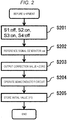
- FIG. 2 is a flowchart illustrating operation of the semiconductor integrated device 1 before shipment.
- the semiconductor integrated device 1 turns off the switching circuit S1, turns on the switching circuit S2, turns on the write circuit S3, and turns off the write circuit S4 (S201) .
- the semiconductor integrated device 1 activates the reference signal generator 200 (S202).
- the semiconductor integrated device 1 sets an output 701 from the correction-value storage circuit 700 to zero (S203) .
- the semiconductor circuit 400 When the semiconductor circuit 400 is operated in this condition (S204), the semiconductor circuit 400 outputs an output value Y1 according to the reference signal 201 from the reference signal generator 200, and Y1 is stored in the initial value storage circuit 500 (S205).
- the flowchart of FIG. 2 has significance in storage of an output value from the semiconductor circuit 400, at a time point before shipment of the semiconductor integrated device 1 (i.e., before the characteristic variation of the semiconductor circuit 400 over time). Accordingly, this operation is preferably performed, for example, in a release test for the semiconductor integrated device 1.
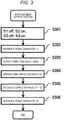
- FIG. 3 is a flowchart illustrating operation of the semiconductor integrated device 1 after shipment.
- the flowchart of FIG. 3 illustrates the process of determining a correction amount for an output value from the semiconductor circuit 400, and the steps of the flowchart are preferably performed, for example, upon activation of the semiconductor integrated device 1.
- the semiconductor integrated device 1 turns off the switching circuit S1, turns on the switching circuit S2, turns off the write circuit S3, and turns on the write circuit S4 (S301) .
- the semiconductor integrated device 1 activates the reference signal generator 200 (S302).
- the semiconductor integrated device 1 sets an output 701 from the correction-value storage circuit 700 to zero (S303) .
- the semiconductor circuit 400 outputs an output value Y2 according to the reference signal 201 from the reference signal generator 200 (S304).
- the difference operation circuit 600 calculates a difference between Y2 and an output 501 representing a value stored in the initial value storage circuit 500 at a time point before shipment, and stores an output 601 representing a result of the calculation in the correction-value storage circuit 700 (S305) .
- the semiconductor integrated device 1 turns off the reference signal generator 200 (S306).
- a variation of the semiconductor circuit 400 over time caused by operation of the semiconductor integrated device 1 after shipment can be obtained for an initial value Y1 determined before shipment.
- the variation can be used as a correction value to correct the characteristic variation of the semiconductor circuit 400 over time.
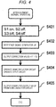
- FIG. 4 is a flowchart illustrating operation of the semiconductor integrated device 1 after shipment.
- the flowchart of FIG. 4 illustrates the steps of correcting a characteristic variation of the semiconductor circuit 400 over time during normal operation of the semiconductor integrated device 1.
- the semiconductor integrated device 1 turns on the switching circuit S1, turns off the switching circuit S2, turns off the write circuit S3, and turns off the write circuit S4 (S401).
- the semiconductor integrated device 1 turns off the reference signal generator 200 (S402).
- the correction-value storage circuit 700 outputs the correction value stored in the flowchart of FIG. 3 (S403).
- the semiconductor integrated device 1 operates the input circuit 100 and the semiconductor circuit 400 (S404).
- the correction circuit 800 applies the correction value output from the correction-value storage circuit 700 to an output 403 from the semiconductor circuit 400 to correct the variation of the output 403 from the semiconductor circuit 400 over time and generate an output 801 after correction (S405).
- the age deterioration of the reference signal generator 200, the initial value storage circuit 500, the difference operation circuit 600, the write circuit S3, and the write circuit S4 can be also prevented.
- stopping the operation of these circuits prevents the age deterioration of these circuits, thus enabling appropriate correction amount detection according to the flowchart of FIG. 3 .
- a specific process will be described.
- a threshold voltage of a semiconductor device such as a metal oxide semiconductor (MOS) transistor
- MOS metal oxide semiconductor
- a gate voltage of a MOS device of the reference signal generator 200 is reduced to zero, thus preventing the variation thereof over time.
- an appropriate switch can be used to change the gate voltage to zero without shutting off the supply voltage, thus obtaining the same effects.
- a heat insulating portion can be provided between the reference signal generator 200 and heat generating portions to prevent age deterioration.
- a representative example of a heat generating portion includes a microcontroller performing control calculation.
- air between the circuits functions as the heat insulating portion.
- another heat-resistant member (structural member, another electrical component having characteristics hardly deteriorated by heat, or the like) may be arranged to be functioned as the heat insulating portion.
- the semiconductor integrated device 1 even when the characteristics of the semiconductor circuit 400 vary with time, the output 801 having the characteristics equal to those in an initial state upon shipment of the semiconductor integrated device 1 can be generated. Accordingly, the semiconductor integrated device 1 can maintain initial performance upon shipment.
- FIG. 5 is a block diagram illustrating a configuration of a vehicle-mounted control device U1 according to a second embodiment of the present invention.
- the vehicle-mounted control device U1 includes the semiconductor integrated device 1 described in the first embodiment, a controller 900, an electromagnetic load drive circuit 902, an electromagnetic load 903, and a load current monitoring circuit 904.
- the controller 900 includes a calculation control device, such as a microcontroller, and outputs a control signal 901 for controlling the electromagnetic load drive circuit 902 in accordance with the output 801 from the semiconductor integrated device 1.
- the electromagnetic load drive circuit 902 drives the electromagnetic load 903 in accordance with the control signal 901.
- the electromagnetic load 903 is a load circuit, such as a solenoid, used for control of vehicle operation.
- the load current monitoring circuit 904 monitors the load current IL running through the electromagnetic load 903, and outputs a result of the monitoring as a monitor signal 905 to the input circuit 100 of the semiconductor integrated device 1.
- the semiconductor circuit 400 performs processing, such as conversion of the monitor signal 905 received by the input circuit 100 to, for example, a digital signal, and outputs the digital signal to the controller 900.
- the controller 900 monitors the load current IL on the basis of the output 801 from the semiconductor circuit 400, and outputs the control signal 901 in accordance with the load current IL. Therefore, the load current IL flowing through the electromagnetic load 903 can be controlled highly accurately.
- FIG. 6 is a graph illustrating an example of a change in load current IL over time.
- the semiconductor circuit 400 sometimes generates an output 801 (current before correction in FIG. 6 ) having characteristics changed due to, for example, a variation over time with the passage of operating time, and thereby representing a value different from the monitor signal 905 received by the input circuit 100. Then, the controller 900 outputs a control signal 901 on the basis of a value different from the actual load current IL.
- the output 403 from the semiconductor circuit 400 is corrected (current after correction in FIG. 6 ) by using the configuration described in the first embodiment and thereby an output from the semiconductor integrated device 1 can be generated with accuracy equal to that set at the factory before shipment.
- an accuracy of a result of monitoring the load current IL being an output from the vehicle-mounted control device U1 can be maintained.
- Operation of determining a correction value described in FIG. 3 is preferably performed, for example, upon activation of the vehicle-mounted control device U1, or performed by the controller 900 by controlling the semiconductor integrated device 1 to perform the steps of the flowchart of FIG. 3 , if necessary.
- the vehicle-mounted control device U1 As described above, according to the vehicle-mounted control device U1 according to the present second embodiment, even when the characteristics of the semiconductor circuit 400 vary with time, the output 801 can be obtained with accuracy equal to that set before shipment. Thus, the failure of the controller 900, wrong operation of a vehicle/vehicle-mounted device as a result of the failure, or the like can be prevented.
- FIG. 7 is a block diagram illustrating a configuration of a vehicle-mounted control device according to a third embodiment of the present invention.
- the vehicle-mounted control device illustrated in FIG. 7 includes a detection circuit IC (integrated circuit) 1 and a controller IC2.
- the detection circuit IC1 includes the semiconductor integrated device 1, which has been described in the first embodiment.
- the controller IC2 includes the controller 900, which has been described in the second embodiment. These circuits are put together in the respective ICs, and thus the number of signal lines of the vehicle-mounted control device can be reduced to reduce the size of the device.
- FIG. 8 is a block diagram illustrating a configuration of a vehicle-mounted control device according to a fourth embodiment of the present invention.
- the vehicle-mounted control device illustrated in FIG. 8 includes a detection circuit IC3 and a controller IC4.
- the detection circuit IC3 includes the input circuit 100, the reference signal generator 200, the input switching circuit 300, and part of the semiconductor circuit 400 (e.g., an amplifier circuit 404) of the configuration described in the first embodiment.
- the controller IC4 includes the rest of the semiconductor circuit 400 (e.g., an AD converter 405), the initial value storage circuit 500, the difference operation circuit 600, the correction-value storage circuit 700, the correction circuit 800, the write circuit S3, the write circuit S4, and further includes the controller 900 described in the second embodiment.
- the vehicle-mounted control device according to the present fourth embodiment can provide effects similar to those of the first to third embodiments.
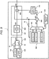
- FIG. 9 is a block diagram illustrating a configuration of a semiconductor integrated device 1 according to a fifth embodiment of the present invention.
- the semiconductor integrated device 1 according to the present fifth embodiment includes a temperature monitor circuit 503 and a selector circuit 505, in addition to the configuration described in the first embodiment.
- the initial value storage circuit 500 stores a plurality of initial values (Y1_1 to Y1_n).
- the other configurations are basically similar to those of the first embodiment, and thus different points will be mainly described below.
- the temperature monitor circuit 503 measures the temperature of the semiconductor integrated device 1 (in particular, the temperature of the semiconductor circuit 400), and outputs a result of the measurement as an output 504.
- the selector circuit 505 selects an initial value corresponding to the output 504 from the temperature monitor circuit 503, from a plurality of initial values stored in the initial value storage circuit 500, and generates the selected initial value as the output 501.
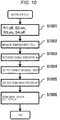
- FIG. 10 is a flowchart illustrating operation of the semiconductor integrated device 1 before shipment.
- step S1002 the temperature of the semiconductor integrated device 1 is measured more than once, and an initial value corresponding to each measurement is stored in the initial value storage circuit 500, in step S1006.
- the other steps are similar to the steps of FIG. 2 .
- the initial value storage circuit 500 can store a pair of each initial value and a measurement result of the initial value from the temperature monitor circuit 503.
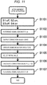
- FIG. 11 is a flowchart illustrating operation of the semiconductor integrated device 1 after shipment.
- the selector circuit 505 acquires a measurement result from the temperature monitor circuit 503, and selects an initial value corresponding to the measurement result.
- the difference operation circuit 600 calculates a difference between the initial value selected by the selector circuit 505 and Y2. The other steps are similar to the steps of FIG. 3 .
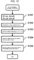
- FIG. 12 is a flowchart illustrating operation of the semiconductor integrated device 1 after shipment.
- the correction-value storage circuit 700 outputs a correction value corresponding to the initial value selected by the selector circuit 505 (corresponding to the measurement result from the temperature monitor circuit 503).
- the other steps are similar to the steps of FIG. 4 .
- the semiconductor integrated device 1 uses a correction value corresponding to a temperature upon operation to correct an output from the semiconductor circuit 400.
- a temperature dependence of a characteristic variation can be corrected.
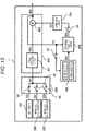
- FIG. 13 is a block diagram illustrating a configuration of a semiconductor integrated device 1 according to a sixth embodiment of the present invention.
- the semiconductor integrated device 1 according to the present sixth embodiment includes a second reference signal generator 202, in addition to the configuration described in the first embodiment.
- the second reference signal generator 202 outputs a second reference signal 203 having a signal level different from that of the reference signal generator 200.
- the input switching circuit 300 includes a switching circuit S5 in addition to the configuration described in the first embodiment.
- the initial value storage circuit 500 can store two initial values (Y1 and Y1').
- the difference operation circuit 600 determines a correction value relating to the above configuration, which is described later.
- the other configurations are basically similar to those of the first embodiment, and thus different points will be mainly described below.
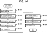
- FIG. 14 is a flowchart illustrating operation of the semiconductor integrated device 1 before shipment.
- the input switching circuit 300 turns on only the switching circuit S2 corresponding to the reference signal generator 200.
- the reference signal generator 200 and the second reference signal generator 202 are operated.
- the initial value storage circuit 500 stores the initial value Y1 corresponding to the reference signal 201.
- the input switching circuit 300 turns on only the switching circuit S5 corresponding to the second reference signal generator 202.
- the initial value storage circuit 500 stores an initial value Y1' corresponding to the second reference signal 203.
- the reference signal generator 200 outputs the reference signal 201 which corresponds to a maximum value within an input range of the semiconductor circuit 400, and the second reference signal generator 202 outputs the second reference signal 203 which corresponds to a minimum value within the input range of the semiconductor circuit 400.
- FIG. 15 is a flowchart illustrating operation of the semiconductor integrated device 1 after shipment.
- the semiconductor integrated device 1 acquires the output value Y2 from the semiconductor circuit 400 corresponding to the reference signal 201.
- the semiconductor integrated device 1 similarly acquires an output value Y2' from the semiconductor circuit 400 corresponding to the second reference signal 203.
- the difference operation circuit 600 calculates an offset variation and a gain variation on the basis of the characteristic variation of the semiconductor circuit 400 over time, in accordance with the following formulas A2 and A3.
- the correction-value storage circuit 700 stores these offset variation and gain variation as correction values.
- Offset variation Y 1 ⁇ Y 2
- Gain variation Y 2 ⁇ Y 2 ' / Y 1 ⁇ Y 1 '
- FIG. 16 is a flowchart illustrating operation of the semiconductor integrated device 1 after shipment.
- the correction circuit 800 uses the offset variation and the gain variation stored in the correction-value storage circuit 700 to correct an offset and a gain of the semiconductor circuit 400.
- the other steps are similar to the steps of FIG. 4 .
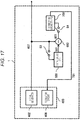
- FIG. 17 is a block diagram illustrating a configuration of a semiconductor integrated device 1 according to a seventh embodiment of the present invention.
- the semiconductor integrated device 1 according to the present seventh embodiment is a device for generating and outputting a signal by itself, and includes the semiconductor circuit 400, the initial value storage circuit 500, the difference operation circuit 600, the correction-value storage circuit 700, the write circuit S3, and the write circuit S4.
- the semiconductor circuit 400 includes a signal generator 402 for generating an output 407, and a regulator circuit 406 for regulating the output 407.
- the regulator circuit 406 corrects the output 407 from the signal generator 402, in accordance with the output 701 from the correction-value storage circuit 700, that is, a correction value.
- the functions of the initial value storage circuit 500, the difference operation circuit 600, the correction-value storage circuit 700, the write circuit S3, and the write circuit S4 are similar to those in the first embodiment.
- FIG. 18 is a flowchart illustrating operation of the semiconductor integrated device 1 before shipment.
- the semiconductor integrated device 1 turns on the write circuit S3, and turns off the write circuit S4 (S1801).
- the semiconductor integrated device 1 sets the output 701 from the correction-value storage circuit 700 to zero (S1802) .
- the regulator circuit 406 performs regulation corresponding to the correction value (e.g., no regulation).
- the initial value storage circuit 500 stores a value corresponding to the output 407 from the signal generator 402 (S1804).
- the steps of the flowchart of FIG. 18 are preferably performed, for example, in a release test for the semiconductor integrated device 1, as in FIG. 2 .
- FIG. 19 is a flowchart illustrating operation of the semiconductor integrated device 1 after shipment. The steps of the flowchart of FIG. 19 are preferably performed, for example, upon activation of the semiconductor integrated device 1, as in FIG. 3 .
- the semiconductor integrated device 1 turns off the write circuit S3, and turns on the write circuit S4 (S1901).
- the semiconductor integrated device 1 sets the output 701 from the correction-value storage circuit 700 to zero (S1902).
- the semiconductor circuit 400 outputs the output value Y2 (S1903) .
- the difference operation circuit 600 calculates a difference between Y2 and the output 501 representing a value stored in the initial value storage circuit 500 at a time point before shipment, and stores the output 601 representing a result of the calculation in the correction-value storage circuit 700 (S1904).
- a variation of the semiconductor circuit 400 over time caused by the operation of the semiconductor integrated device 1 after shipment can be obtained for the initial value Y1 determined before shipment.
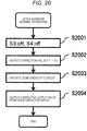
- FIG. 20 is a flowchart illustrating operation of the semiconductor integrated device 1 after shipment.
- the flowchart of FIG. 20 illustrates the steps of correcting a characteristic variation of the semiconductor circuit 400 over time during normal operation of the semiconductor integrated device 1, as in FIG. 4 .
- the semiconductor integrated device 1 turns off the write circuit S3, and turns off the write circuit S4 (S2001).
- Step S2002 to S2004 are similar to steps S403 to S405.
- the semiconductor integrated device 1 according to the present seventh embodiment can maintain the characteristics of the output 407 upon shipment, as in the first embodiment. Furthermore, the operations of the initial value storage circuit 500, the difference operation circuit 600, the write circuit S3, and the write circuit S4 are stopped, and thereby the age deterioration of these circuits can be also prevented, as in the first embodiment.
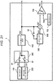
- FIG. 21 is a block diagram illustrating a configuration of a semiconductor integrated device 1 according to an eighth embodiment of the present invention.
- the semiconductor integrated device 1 according to the present eighth embodiment includes the input circuit 100, the reference signal generator 200, the input switching circuit 300, the semiconductor circuit 400, the initial value storage circuit 500, the difference operation circuit 600, a threshold generation circuit 702, a determination circuit 703, and the write circuit S3.
- the functions of the input circuit 100, the reference signal generator 200, the input switching circuit 300, the initial value storage circuit 500, the difference operation circuit 600, and the write circuit S3 are basically similar to those of the first embodiment, and thus different points about the other configurations will be described below.
- the semiconductor circuit 400 does not include the correction circuit 800. Accordingly, the difference operation circuit 600 calculates a difference between the output 403 from the semiconductor circuit 400 and the initial value Y1 stored in the initial value storage circuit 500.
- the threshold generation circuit 702 generates a threshold value previously set, and generates an output 704 representing the threshold value.
- the determination circuit 703 compares the output 601 from the difference operation circuit 600 and the output 704 from the threshold generation circuit 702, and outputs a determination result 705.
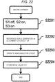
- FIG. 22 is a flowchart illustrating operation of the semiconductor integrated device 1 before shipment.
- the semiconductor integrated device 1 turns off the switching circuit S1, turns on the switching circuit S2, and turns on the write circuit S3 (S2201) .
- the semiconductor integrated device 1 activates the reference signal generator 200, and turns off the determination circuit 703 (S2202) .
- the semiconductor circuit 400 When the semiconductor circuit 400 is operated in this condition (S2203), the semiconductor circuit 400 outputs an output value Y1 according to the reference signal 201 from the reference signal generator 200, and Y1 is stored in the initial value storage circuit 500 (S2204) .
- the steps of the flowchart of FIG. 22 are preferably performed, for example, in a release test for the semiconductor integrated device 1, as in FIG. 2 .
- FIG. 23 is a flowchart illustrating operation of the semiconductor integrated device 1 after shipment. The steps of the flowchart of FIG. 23 are preferably performed, for example, upon activation of the semiconductor integrated device 1, as in FIG. 3 .
- the semiconductor integrated device 1 turns off the switching circuit S1, turns on the switching circuit S2, and turns off the write circuit S3 (S2301).
- the semiconductor integrated device 1 activates the reference signal generator 200 and the determination circuit 703 (S2302).
- the semiconductor circuit 400 outputs an output value Y2 according to the reference signal 201 from the reference signal generator 200 (S2303).
- the difference operation circuit 600 calculates a difference between Y2 and the output 501 representing a value stored in the initial value storage circuit 500 at a time point before shipment, and transmits the output 601 representing a result of the calculation to the determination circuit 703 (S2304).
- the determination circuit 703 outputs a result of comparison between the outputs 601 and 704 (S2305).
- the semiconductor integrated device 1 turns off the reference signal generator 200 and the determination circuit 703 (S2306) .
- the controller of the vehicle-mounted control device can determine an abnormal condition of the semiconductor integrated device 1 on the basis of the determination result 705.
- error notification of for example turning on of an alarm indicator can be made.
- FIG. 24 is a flowchart illustrating operation of the semiconductor integrated device 1 after shipment.
- the flowchart of FIG. 24 illustrates the steps of correcting a characteristic variation of the semiconductor circuit 400 over time during normal operation of the semiconductor integrated device 1.
- the semiconductor integrated device 1 turns on the switching circuit S1, turns off the switching circuit S2, and turns off the write circuit S3 (S2401).
- the semiconductor integrated device 1 turns off the reference signal generator 200 and the determination circuit 703 (S2402).
- the semiconductor integrated device 1 operates the input circuit 100 and the semiconductor circuit 400 (S2403) .
- the operations of the initial value storage circuit 500, the difference operation circuit 600, the determination circuit 703, and the threshold generation circuit 702 are stopped, and thereby the age deterioration of these circuits can be also prevented, as in the first embodiment.
- the semiconductor integrated device 1 can detect the age deterioration of the semiconductor circuit 400 by using the determination circuit 703. Furthermore, on the basis of a detection result, the following measures can be taken (a) reporting an abnormal condition of the semiconductor circuit 400 to a vehicle driver, (b) recording an abnormal log, or (c) performing fail-safe processing (e.g., suspending control of a vehicle-mounted device or a vehicle).
- fail-safe processing e.g., suspending control of a vehicle-mounted device or a vehicle.
- the present invention is not limited to the examples described above, and can include various modifications.
- the above examples are described in detail for convenience to understand the present invention, and therefore, the present invention is not necessarily limited to a configuration including all of the configurations described above.
- part of a configuration according to an example can be replaced with a configuration according to another example, and a configuration according to an example can be also applied to a configuration according to another example.
- addition, elimination, or substitution of another configuration may be made for part of a configuration according to each example.
- control lines or information lines considered to be necessary for description are described, and all control lines or information lines required for a product are not always illustrated. Any of analog signal and digital signal can be input to or output from each component circuit, with similar effects.
- the component elements of the semiconductor integrated device 1 may be formed on the same semiconductor chip to be configured as an integrated circuit, or may be separated to be mounted as a plurality of components.
- the operation of the semiconductor integrated device 1 may be controlled in accordance with a command from a calculation control device such as the controller 900 or the semiconductor integrated device 1 may include a control device for controlling the operation of the semiconductor integrated device 1.
Landscapes
- Engineering & Computer Science (AREA)
- Physics & Mathematics (AREA)
- General Physics & Mathematics (AREA)
- Automation & Control Theory (AREA)
- General Engineering & Computer Science (AREA)
- Computer Hardware Design (AREA)
- Mechanical Engineering (AREA)
- Microelectronics & Electronic Packaging (AREA)
- Theoretical Computer Science (AREA)
- Power Engineering (AREA)
- Transportation (AREA)
- Human Computer Interaction (AREA)
- Condensed Matter Physics & Semiconductors (AREA)
- Manufacturing & Machinery (AREA)
- Quality & Reliability (AREA)
- Environmental & Geological Engineering (AREA)
- Semiconductor Integrated Circuits (AREA)
- Analogue/Digital Conversion (AREA)
- Test And Diagnosis Of Digital Computers (AREA)
Abstract
Description
- The present invention relates to a vehicle-mounted integrated circuit and a vehicle-mounted control device using the vehicle-mounted integrated circuit.
- In recent years, various devices mounted on vehicles have been electronically controlled, and, for example, in function of monitoring output values from power generation units, sensors, or drive devices of vehicle-mounted control devices, semiconductor integrated circuits have been widely used.
- A long time operation of these semiconductor integrated circuits gradually changes the characteristics thereof due to influence of hot carrier, negative bias temperature instability (NBTI), wire migration, or the like, and thus, the characteristics of vehicle-mounted control devices may be deteriorated and the deterioration may influence vehicle control.
- Technologies for detecting the presence/absence of failure by self tests or the like for semiconductor integrated circuits after shipment have been disclosed. For example, the following
PTL 1 describes a semiconductor integrated circuit "configured to supply outputs at three levels of the high level, the low level, and the intermediate level generated by the diagnostic signal generation circuit, to an analog signal input terminal of the A/D converter to perform A/D conversion, the semiconductor integrated circuit diagnosing success or failure in performance of the A/D converter on the basis of a digital output from the A/D converter" (see claim 1). - PTL 1:
JP 2007-309773 A - In
PTL 1, as seen from the description "diagnosing success or failure in performance of the A/D converter on the basis of a digital output from the A/D converter", normal operation disabled by an abnormal condition generated in the circuit can be detected, but detection of a change in characteristics due to the age deterioration or the like of the circuit is not taken into consideration. Therefore, the lifetimes of the semiconductor integrated circuit and a vehicle-mounted control device using the semiconductor integrated circuit may be reduced relative to expected lifetimes thereof. - The present invention has been made in view of the above problems, and an object of the present invention is to provide a semiconductor integrated circuit which can continuously and stably generate an output value even after shipment and a vehicle-mounted control device using the semiconductor integrated circuit.
- The present invention includes a reference signal generation unit for outputting a reference signal, and detects the operation state of a semiconductor circuit on the basis of a difference between output values from the semiconductor circuit corresponding to the reference signals output at two different time points by the reference signal generation unit.
- According to the present invention, even when the characteristics of a semiconductor circuit varies with time, the variation can be detected and output values can be stably generated continuously. Problems, configurations, and effects other than the above description will be made clear by the following description of the embodiments.
-
- [
FIG. 1] FIG. 1 is a block diagram illustrating a configuration of a semiconductor integrateddevice 1 according to a first embodiment. - [
FIG. 2] FIG. 2 is a flowchart illustrating operation of the semiconductor integrateddevice 1 before shipment. - [
FIG. 3] FIG. 3 is a flowchart illustrating operation of the semiconductor integrateddevice 1 after shipment. - [
FIG. 4] FIG. 4 is a flowchart illustrating operation of the semiconductor integrateddevice 1 after shipment. - [
FIG. 5] FIG. 5 is a block diagram illustrating a configuration of a vehicle-mounted control device U1 according to a second embodiment. - [
FIG. 6] FIG. 6 is a graph illustrating an example of a change in load current IL over time. - [
FIG. 7] FIG. 7 is a block diagram illustrating a configuration of a vehicle-mounted control device according to a third embodiment. - [
FIG. 8] FIG. 8 is a block diagram illustrating a configuration of a vehicle-mounted control device according to a fourth embodiment. - [
FIG. 9] FIG. 9 is a block diagram illustrating a configuration of a semiconductor integrateddevice 1 according to a fifth embodiment. - [
FIG. 10] FIG. 10 is a flowchart illustrating operation of the semiconductor integrateddevice 1 before shipment. - [
FIG. 11] FIG. 11 is a flowchart illustrating operation of the semiconductor integrateddevice 1 after shipment. - [
FIG. 12] FIG. 12 is a flowchart illustrating operation of the semiconductor integrateddevice 1 after shipment. - [
FIG. 13] FIG. 13 is a block diagram illustrating a configuration of a semiconductor integrateddevice 1 according to a sixth embodiment. - [
FIG. 14] FIG. 14 is a flowchart illustrating operation of the semiconductor integrateddevice 1 before shipment. - [
FIG. 15] FIG. 15 is a flowchart illustrating operation of the semiconductor integrateddevice 1 after shipment. - [
FIG. 16] FIG. 16 is a flowchart illustrating operation of the semiconductor integrateddevice 1 after shipment. - [
FIG. 17] FIG. 17 is a block diagram illustrating a configuration of a semiconductor integrateddevice 1 according to a seventh embodiment. - [
FIG. 18] FIG. 18 is a flowchart illustrating operation of the semiconductor integrateddevice 1 before shipment. - [
FIG. 19] FIG. 19 is a flowchart illustrating operation of the semiconductor integrateddevice 1 after shipment. - [
FIG. 20] FIG. 20 is a flowchart illustrating operation of the semiconductor integrateddevice 1 after shipment. - [
FIG. 21] FIG. 21 is a block diagram illustrating a configuration of a semiconductor integrateddevice 1 according to an eighth embodiment. - [
FIG. 22] FIG. 22 is a flowchart illustrating operation of the semiconductor integrateddevice 1 before shipment. - [
FIG. 23] FIG. 23 is a flowchart illustrating operation of the semiconductor integrateddevice 1 after shipment. - [
FIG. 24] FIG. 24 is a flowchart illustrating operation of the semiconductor integrateddevice 1 after shipment. -
FIG. 1 is a block diagram illustrating a configuration of a semiconductor integrateddevice 1 according to a first embodiment of the present invention. The semiconductor integrateddevice 1 is a device mounted, for example, on a vehicle and outputting a signal used to control a vehicle-mounted device. The semiconductor integrateddevice 1 includes aninput circuit 100, areference signal generator 200, aninput switching circuit 300, asemiconductor circuit 400, an initialvalue storage circuit 500, adifference operation circuit 600, a correction-value storage circuit 700, a write circuit S3, and a write circuit S4. - The
input circuit 100 is a circuit, such as a sensor circuit of a vehicle-mounted control device or a drive current monitoring circuit of an electromagnetic load drive device, for providing a signal being an input value to thesemiconductor circuit 400. Thereference signal generator 200 generates a reference signal used as a reference for measurement of a characteristic variation of thesemiconductor circuit 400 over time. Theinput switching circuit 300 includes switching circuits S1 and S2, and switches the switching circuits S1 and S2 to transmit anoutput 101 from theinput circuit 100 or areference signal 201 from thereference signal generator 200 to thesemiconductor circuit 400. Thesemiconductor circuit 400 is a circuit for outputting a signal used to control, for example, a vehicle-mounted device, and includes asignal processing circuit 401 and acorrection circuit 800. The initialvalue storage circuit 500 is a storage element, such as a memory device, and stores an output value from thecorrection circuit 800. The write circuit S3 switches writing of a value to the initialvalue storage circuit 500. Thedifference operation circuit 600 calculates a difference between anoutput 501 from the initialvalue storage circuit 500 and anoutput 801 from thecorrection circuit 800. The correction-value storage circuit 700 is a storage element, such as a register, and stores anoutput 601 from thedifference operation circuit 600. The write circuit S4 switches writing of a value to the correction-value storage circuit 700. - The
signal processing circuit 401 is a circuit performing for example signal conversion on anoutput 301 from theinput switching circuit 300, and includes, for example, an AD converter. Thecorrection circuit 800 uses anoutput 701 from the correction-value storage circuit 700 to correct anoutput 403 from the signal processing circuit 401 (e.g., add both outputs to correct a difference between both output values), and generates anoutput 801 as a result of the correction. -
FIG. 2 is a flowchart illustrating operation of the semiconductor integrateddevice 1 before shipment. Before shipment, the semiconductor integrateddevice 1 turns off the switching circuit S1, turns on the switching circuit S2, turns on the write circuit S3, and turns off the write circuit S4 (S201) . The semiconductor integrateddevice 1 activates the reference signal generator 200 (S202). The semiconductor integrateddevice 1 sets anoutput 701 from the correction-value storage circuit 700 to zero (S203) . When thesemiconductor circuit 400 is operated in this condition (S204), thesemiconductor circuit 400 outputs an output value Y1 according to thereference signal 201 from thereference signal generator 200, and Y1 is stored in the initial value storage circuit 500 (S205). - The flowchart of
FIG. 2 has significance in storage of an output value from thesemiconductor circuit 400, at a time point before shipment of the semiconductor integrated device 1 (i.e., before the characteristic variation of thesemiconductor circuit 400 over time). Accordingly, this operation is preferably performed, for example, in a release test for the semiconductor integrateddevice 1. -
FIG. 3 is a flowchart illustrating operation of the semiconductor integrateddevice 1 after shipment. The flowchart ofFIG. 3 illustrates the process of determining a correction amount for an output value from thesemiconductor circuit 400, and the steps of the flowchart are preferably performed, for example, upon activation of the semiconductor integrateddevice 1. - The semiconductor integrated
device 1 turns off the switching circuit S1, turns on the switching circuit S2, turns off the write circuit S3, and turns on the write circuit S4 (S301) . The semiconductor integrateddevice 1 activates the reference signal generator 200 (S302). The semiconductor integrateddevice 1 sets anoutput 701 from the correction-value storage circuit 700 to zero (S303) . When thesemiconductor circuit 400 is operated in this condition, thesemiconductor circuit 400 outputs an output value Y2 according to thereference signal 201 from the reference signal generator 200 (S304). Thedifference operation circuit 600 calculates a difference between Y2 and anoutput 501 representing a value stored in the initialvalue storage circuit 500 at a time point before shipment, and stores anoutput 601 representing a result of the calculation in the correction-value storage circuit 700 (S305) . The semiconductor integrateddevice 1 turns off the reference signal generator 200 (S306). - In the flowchart of
FIG. 3 , a variation of thesemiconductor circuit 400 over time caused by operation of the semiconductor integrateddevice 1 after shipment can be obtained for an initial value Y1 determined before shipment. The variation can be used as a correction value to correct the characteristic variation of thesemiconductor circuit 400 over time. The correction value can be calculated, for example, on the basis of the following formula (A1) : correction value = Y1 - Y2 ... (A1) -
FIG. 4 is a flowchart illustrating operation of the semiconductor integrateddevice 1 after shipment. The flowchart ofFIG. 4 illustrates the steps of correcting a characteristic variation of thesemiconductor circuit 400 over time during normal operation of the semiconductor integrateddevice 1. - The semiconductor integrated
device 1 turns on the switching circuit S1, turns off the switching circuit S2, turns off the write circuit S3, and turns off the write circuit S4 (S401). The semiconductor integrateddevice 1 turns off the reference signal generator 200 (S402). The correction-value storage circuit 700 outputs the correction value stored in the flowchart ofFIG. 3 (S403). The semiconductor integrateddevice 1 operates theinput circuit 100 and the semiconductor circuit 400 (S404). Thecorrection circuit 800 applies the correction value output from the correction-value storage circuit 700 to anoutput 403 from thesemiconductor circuit 400 to correct the variation of theoutput 403 from thesemiconductor circuit 400 over time and generate anoutput 801 after correction (S405). - In addition to the variation of the
semiconductor circuit 400 over time, the age deterioration of thereference signal generator 200, the initialvalue storage circuit 500, thedifference operation circuit 600, the write circuit S3, and the write circuit S4 can be also prevented. For example, in a normal operation state, stopping the operation of these circuits prevents the age deterioration of these circuits, thus enabling appropriate correction amount detection according to the flowchart ofFIG. 3 . Hereinafter, a specific process will be described. - It is known that a threshold voltage of a semiconductor device, such as a metal oxide semiconductor (MOS) transistor, varies with time while a voltage is applied to the gate terminal. When a supply voltage to the
reference signal generator 200 is shut off, a gate voltage of a MOS device of thereference signal generator 200 is reduced to zero, thus preventing the variation thereof over time. Alternatively, an appropriate switch can be used to change the gate voltage to zero without shutting off the supply voltage, thus obtaining the same effects. - It is known that a semiconductor device (e.g., MOS transistor) of the
reference signal generator 200 exposed to high temperature varies with time at an accelerating rate. Therefore, a heat insulating portion can be provided between thereference signal generator 200 and heat generating portions to prevent age deterioration. Here, a representative example of a heat generating portion includes a microcontroller performing control calculation. When thereference signal generator 200 is separated as much as possible from these heat generating portions, air between the circuits functions as the heat insulating portion. Alternately, between thereference signal generator 200 and the heat generating portions, another heat-resistant member(structural member, another electrical component having characteristics hardly deteriorated by heat, or the like) may be arranged to be functioned as the heat insulating portion. - As described above, according to the semiconductor integrated
device 1 according to the present first embodiment, even when the characteristics of thesemiconductor circuit 400 vary with time, theoutput 801 having the characteristics equal to those in an initial state upon shipment of the semiconductor integrateddevice 1 can be generated. Accordingly, the semiconductor integrateddevice 1 can maintain initial performance upon shipment. -
FIG. 5 is a block diagram illustrating a configuration of a vehicle-mounted control device U1 according to a second embodiment of the present invention. The vehicle-mounted control device U1 includes the semiconductor integrateddevice 1 described in the first embodiment, acontroller 900, an electromagneticload drive circuit 902, anelectromagnetic load 903, and a loadcurrent monitoring circuit 904. - The
controller 900 includes a calculation control device, such as a microcontroller, and outputs acontrol signal 901 for controlling the electromagneticload drive circuit 902 in accordance with theoutput 801 from the semiconductor integrateddevice 1. The electromagneticload drive circuit 902 drives theelectromagnetic load 903 in accordance with thecontrol signal 901. Theelectromagnetic load 903 is a load circuit, such as a solenoid, used for control of vehicle operation. The loadcurrent monitoring circuit 904 monitors the load current IL running through theelectromagnetic load 903, and outputs a result of the monitoring as amonitor signal 905 to theinput circuit 100 of the semiconductor integrateddevice 1. - The
semiconductor circuit 400 performs processing, such as conversion of themonitor signal 905 received by theinput circuit 100 to, for example, a digital signal, and outputs the digital signal to thecontroller 900. Thecontroller 900 monitors the load current IL on the basis of theoutput 801 from thesemiconductor circuit 400, and outputs thecontrol signal 901 in accordance with the load current IL. Therefore, the load current IL flowing through theelectromagnetic load 903 can be controlled highly accurately. -
FIG. 6 is a graph illustrating an example of a change in load current IL over time. Thesemiconductor circuit 400 sometimes generates an output 801 (current before correction inFIG. 6 ) having characteristics changed due to, for example, a variation over time with the passage of operating time, and thereby representing a value different from themonitor signal 905 received by theinput circuit 100. Then, thecontroller 900 outputs acontrol signal 901 on the basis of a value different from the actual load current IL. - The
output 403 from thesemiconductor circuit 400 is corrected (current after correction inFIG. 6 ) by using the configuration described in the first embodiment and thereby an output from the semiconductor integrateddevice 1 can be generated with accuracy equal to that set at the factory before shipment. Thus, an accuracy of a result of monitoring the load current IL being an output from the vehicle-mounted control device U1 can be maintained. - Operation of determining a correction value described in
FIG. 3 is preferably performed, for example, upon activation of the vehicle-mounted control device U1, or performed by thecontroller 900 by controlling the semiconductor integrateddevice 1 to perform the steps of the flowchart ofFIG. 3 , if necessary. - As described above, according to the vehicle-mounted control device U1 according to the present second embodiment, even when the characteristics of the
semiconductor circuit 400 vary with time, theoutput 801 can be obtained with accuracy equal to that set before shipment. Thus, the failure of thecontroller 900, wrong operation of a vehicle/vehicle-mounted device as a result of the failure, or the like can be prevented. -
FIG. 7 is a block diagram illustrating a configuration of a vehicle-mounted control device according to a third embodiment of the present invention. The vehicle-mounted control device illustrated inFIG. 7 includes a detection circuit IC (integrated circuit) 1 and a controller IC2. The detection circuit IC1 includes the semiconductor integrateddevice 1, which has been described in the first embodiment. The controller IC2 includes thecontroller 900, which has been described in the second embodiment. These circuits are put together in the respective ICs, and thus the number of signal lines of the vehicle-mounted control device can be reduced to reduce the size of the device. -
FIG. 8 is a block diagram illustrating a configuration of a vehicle-mounted control device according to a fourth embodiment of the present invention. The vehicle-mounted control device illustrated inFIG. 8 includes a detection circuit IC3 and a controller IC4. The detection circuit IC3 includes theinput circuit 100, thereference signal generator 200, theinput switching circuit 300, and part of the semiconductor circuit 400 (e.g., an amplifier circuit 404) of the configuration described in the first embodiment. The controller IC4 includes the rest of the semiconductor circuit 400 (e.g., an AD converter 405), the initialvalue storage circuit 500, thedifference operation circuit 600, the correction-value storage circuit 700, thecorrection circuit 800, the write circuit S3, the write circuit S4, and further includes thecontroller 900 described in the second embodiment. The vehicle-mounted control device according to the present fourth embodiment can provide effects similar to those of the first to third embodiments. -
FIG. 9 is a block diagram illustrating a configuration of a semiconductor integrateddevice 1 according to a fifth embodiment of the present invention. The semiconductor integrateddevice 1 according to the present fifth embodiment includes atemperature monitor circuit 503 and aselector circuit 505, in addition to the configuration described in the first embodiment. Furthermore, the initialvalue storage circuit 500 stores a plurality of initial values (Y1_1 to Y1_n). The other configurations are basically similar to those of the first embodiment, and thus different points will be mainly described below. - The
temperature monitor circuit 503 measures the temperature of the semiconductor integrated device 1 (in particular, the temperature of the semiconductor circuit 400), and outputs a result of the measurement as anoutput 504. Theselector circuit 505 selects an initial value corresponding to theoutput 504 from thetemperature monitor circuit 503, from a plurality of initial values stored in the initialvalue storage circuit 500, and generates the selected initial value as theoutput 501. -
FIG. 10 is a flowchart illustrating operation of the semiconductor integrateddevice 1 before shipment. In step S1002, the temperature of the semiconductor integrateddevice 1 is measured more than once, and an initial value corresponding to each measurement is stored in the initialvalue storage circuit 500, in step S1006. The other steps are similar to the steps ofFIG. 2 . For preparation of diverse initial values, it is desirable to store initial values which are acquired in temperature conditions within as wide operation temperature range as possible of, for example, the semiconductor integrated device 1 (in particular, the semiconductor circuit 400). The initialvalue storage circuit 500 can store a pair of each initial value and a measurement result of the initial value from thetemperature monitor circuit 503. -
FIG. 11 is a flowchart illustrating operation of the semiconductor integrateddevice 1 after shipment. In step S1105, theselector circuit 505 acquires a measurement result from thetemperature monitor circuit 503, and selects an initial value corresponding to the measurement result. In step S1106, thedifference operation circuit 600 calculates a difference between the initial value selected by theselector circuit 505 and Y2. The other steps are similar to the steps ofFIG. 3 . -
FIG. 12 is a flowchart illustrating operation of the semiconductor integrateddevice 1 after shipment. In step S1203, the correction-value storage circuit 700 outputs a correction value corresponding to the initial value selected by the selector circuit 505 (corresponding to the measurement result from the temperature monitor circuit 503). The other steps are similar to the steps ofFIG. 4 . - As described above, the semiconductor integrated
device 1 according to the present fifth embodiment uses a correction value corresponding to a temperature upon operation to correct an output from thesemiconductor circuit 400. Thus, a temperature dependence of a characteristic variation can be corrected. -
FIG. 13 is a block diagram illustrating a configuration of a semiconductor integrateddevice 1 according to a sixth embodiment of the present invention. The semiconductor integrateddevice 1 according to the present sixth embodiment includes a secondreference signal generator 202, in addition to the configuration described in the first embodiment. The secondreference signal generator 202 outputs asecond reference signal 203 having a signal level different from that of thereference signal generator 200. Theinput switching circuit 300 includes a switching circuit S5 in addition to the configuration described in the first embodiment. The initialvalue storage circuit 500 can store two initial values (Y1 and Y1'). Thedifference operation circuit 600 determines a correction value relating to the above configuration, which is described later. The other configurations are basically similar to those of the first embodiment, and thus different points will be mainly described below. -
FIG. 14 is a flowchart illustrating operation of the semiconductor integrateddevice 1 before shipment. In step S1401, theinput switching circuit 300 turns on only the switching circuit S2 corresponding to thereference signal generator 200. In step S1402, thereference signal generator 200 and the secondreference signal generator 202 are operated. Thereby, the initialvalue storage circuit 500 stores the initial value Y1 corresponding to thereference signal 201. In step S1406, theinput switching circuit 300 turns on only the switching circuit S5 corresponding to the secondreference signal generator 202. When thesemiconductor circuit 400 is operated in this condition (S1407), the initialvalue storage circuit 500 stores an initial value Y1' corresponding to thesecond reference signal 203. - From the viewpoint of correction value calculation, which is described later, it is desirable that the
reference signal generator 200 outputs thereference signal 201 which corresponds to a maximum value within an input range of thesemiconductor circuit 400, and the secondreference signal generator 202 outputs thesecond reference signal 203 which corresponds to a minimum value within the input range of thesemiconductor circuit 400. -
FIG. 15 is a flowchart illustrating operation of the semiconductor integrateddevice 1 after shipment. In step S1501 to S1504, the semiconductor integrateddevice 1 acquires the output value Y2 from thesemiconductor circuit 400 corresponding to thereference signal 201. In step S1505 to S1507, the semiconductor integrateddevice 1 similarly acquires an output value Y2' from thesemiconductor circuit 400 corresponding to thesecond reference signal 203. In step S1508, thedifference operation circuit 600 calculates an offset variation and a gain variation on the basis of the characteristic variation of thesemiconductor circuit 400 over time, in accordance with the following formulas A2 and A3. The correction-value storage circuit 700 stores these offset variation and gain variation as correction values.

-
FIG. 16 is a flowchart illustrating operation of the semiconductor integrateddevice 1 after shipment. In step S1603, thecorrection circuit 800 uses the offset variation and the gain variation stored in the correction-value storage circuit 700 to correct an offset and a gain of thesemiconductor circuit 400. The other steps are similar to the steps ofFIG. 4 . -
FIG. 17 is a block diagram illustrating a configuration of a semiconductor integrateddevice 1 according to a seventh embodiment of the present invention. The semiconductor integrateddevice 1 according to the present seventh embodiment is a device for generating and outputting a signal by itself, and includes thesemiconductor circuit 400, the initialvalue storage circuit 500, thedifference operation circuit 600, the correction-value storage circuit 700, the write circuit S3, and the write circuit S4. - In the present seventh embodiment, the
semiconductor circuit 400 includes asignal generator 402 for generating anoutput 407, and aregulator circuit 406 for regulating theoutput 407. Theregulator circuit 406 corrects theoutput 407 from thesignal generator 402, in accordance with theoutput 701 from the correction-value storage circuit 700, that is, a correction value. The functions of the initialvalue storage circuit 500, thedifference operation circuit 600, the correction-value storage circuit 700, the write circuit S3, and the write circuit S4 are similar to those in the first embodiment. -
FIG. 18 is a flowchart illustrating operation of the semiconductor integrateddevice 1 before shipment. Before shipment, the semiconductor integrateddevice 1 turns on the write circuit S3, and turns off the write circuit S4 (S1801). The semiconductor integrateddevice 1 sets theoutput 701 from the correction-value storage circuit 700 to zero (S1802) . Theregulator circuit 406 performs regulation corresponding to the correction value (e.g., no regulation). When thesemiconductor circuit 400 is operated in this condition (S1803), the initialvalue storage circuit 500 stores a value corresponding to theoutput 407 from the signal generator 402 (S1804). The steps of the flowchart ofFIG. 18 are preferably performed, for example, in a release test for the semiconductor integrateddevice 1, as inFIG. 2 . -
FIG. 19 is a flowchart illustrating operation of the semiconductor integrateddevice 1 after shipment. The steps of the flowchart ofFIG. 19 are preferably performed, for example, upon activation of the semiconductor integrateddevice 1, as inFIG. 3 . - The semiconductor integrated
device 1 turns off the write circuit S3, and turns on the write circuit S4 (S1901). The semiconductor integrateddevice 1 sets theoutput 701 from the correction-value storage circuit 700 to zero (S1902). When thesemiconductor circuit 400 is operated in this condition, thesemiconductor circuit 400 outputs the output value Y2 (S1903) . Thedifference operation circuit 600 calculates a difference between Y2 and theoutput 501 representing a value stored in the initialvalue storage circuit 500 at a time point before shipment, and stores theoutput 601 representing a result of the calculation in the correction-value storage circuit 700 (S1904). In accordance with the flowchart ofFIG. 19 , a variation of thesemiconductor circuit 400 over time caused by the operation of the semiconductor integrateddevice 1 after shipment can be obtained for the initial value Y1 determined before shipment. -
FIG. 20 is a flowchart illustrating operation of the semiconductor integrateddevice 1 after shipment. The flowchart ofFIG. 20 illustrates the steps of correcting a characteristic variation of thesemiconductor circuit 400 over time during normal operation of the semiconductor integrateddevice 1, as inFIG. 4 . The semiconductor integrateddevice 1 turns off the write circuit S3, and turns off the write circuit S4 (S2001). Step S2002 to S2004 are similar to steps S403 to S405. - As described above, even when the characteristics of the
semiconductor circuit 400 and the correction-value storage circuit 700 vary with time, the semiconductor integrateddevice 1 according to the present seventh embodiment can maintain the characteristics of theoutput 407 upon shipment, as in the first embodiment. Furthermore, the operations of the initialvalue storage circuit 500, thedifference operation circuit 600, the write circuit S3, and the write circuit S4 are stopped, and thereby the age deterioration of these circuits can be also prevented, as in the first embodiment. -
FIG. 21 is a block diagram illustrating a configuration of a semiconductor integrateddevice 1 according to an eighth embodiment of the present invention. The semiconductor integrateddevice 1 according to the present eighth embodiment includes theinput circuit 100, thereference signal generator 200, theinput switching circuit 300, thesemiconductor circuit 400, the initialvalue storage circuit 500, thedifference operation circuit 600, athreshold generation circuit 702, adetermination circuit 703, and the write circuit S3. The functions of theinput circuit 100, thereference signal generator 200, theinput switching circuit 300, the initialvalue storage circuit 500, thedifference operation circuit 600, and the write circuit S3 are basically similar to those of the first embodiment, and thus different points about the other configurations will be described below. - In the present eighth embodiment, unlike the first embodiment, the
semiconductor circuit 400 does not include thecorrection circuit 800. Accordingly, thedifference operation circuit 600 calculates a difference between theoutput 403 from thesemiconductor circuit 400 and the initial value Y1 stored in the initialvalue storage circuit 500. - The
threshold generation circuit 702 generates a threshold value previously set, and generates anoutput 704 representing the threshold value. Thedetermination circuit 703 compares theoutput 601 from thedifference operation circuit 600 and theoutput 704 from thethreshold generation circuit 702, and outputs adetermination result 705. -
FIG. 22 is a flowchart illustrating operation of the semiconductor integrateddevice 1 before shipment. Before shipment, the semiconductor integrateddevice 1 turns off the switching circuit S1, turns on the switching circuit S2, and turns on the write circuit S3 (S2201) . The semiconductor integrateddevice 1 activates thereference signal generator 200, and turns off the determination circuit 703 (S2202) . When thesemiconductor circuit 400 is operated in this condition (S2203), thesemiconductor circuit 400 outputs an output value Y1 according to thereference signal 201 from thereference signal generator 200, and Y1 is stored in the initial value storage circuit 500 (S2204) . The steps of the flowchart ofFIG. 22 are preferably performed, for example, in a release test for the semiconductor integrateddevice 1, as inFIG. 2 . -
FIG. 23 is a flowchart illustrating operation of the semiconductor integrateddevice 1 after shipment. The steps of the flowchart ofFIG. 23 are preferably performed, for example, upon activation of the semiconductor integrateddevice 1, as inFIG. 3 . - The semiconductor integrated
device 1 turns off the switching circuit S1, turns on the switching circuit S2, and turns off the write circuit S3 (S2301). The semiconductor integrateddevice 1 activates thereference signal generator 200 and the determination circuit 703 (S2302). When thesemiconductor circuit 400 is operated in this condition, thesemiconductor circuit 400 outputs an output value Y2 according to thereference signal 201 from the reference signal generator 200 (S2303). Thedifference operation circuit 600 calculates a difference between Y2 and theoutput 501 representing a value stored in the initialvalue storage circuit 500 at a time point before shipment, and transmits theoutput 601 representing a result of the calculation to the determination circuit 703 (S2304). Thedetermination circuit 703 outputs a result of comparison between theoutputs 601 and 704 (S2305). The semiconductor integrateddevice 1 turns off thereference signal generator 200 and the determination circuit 703 (S2306) . - When the semiconductor integrated
device 1 according to the present eighth embodiment is mounted, for example, to a vehicle-mounted control device, the controller of the vehicle-mounted control device can determine an abnormal condition of the semiconductor integrateddevice 1 on the basis of thedetermination result 705. Thus, error notification of for example turning on of an alarm indicator can be made. -
FIG. 24 is a flowchart illustrating operation of the semiconductor integrateddevice 1 after shipment. The flowchart ofFIG. 24 illustrates the steps of correcting a characteristic variation of thesemiconductor circuit 400 over time during normal operation of the semiconductor integrateddevice 1. - The semiconductor integrated
device 1 turns on the switching circuit S1, turns off the switching circuit S2, and turns off the write circuit S3 (S2401). The semiconductor integrateddevice 1 turns off thereference signal generator 200 and the determination circuit 703 (S2402). The semiconductor integrateddevice 1 operates theinput circuit 100 and the semiconductor circuit 400 (S2403) . The operations of the initialvalue storage circuit 500, thedifference operation circuit 600, thedetermination circuit 703, and thethreshold generation circuit 702 are stopped, and thereby the age deterioration of these circuits can be also prevented, as in the first embodiment. - As described above, the semiconductor integrated
device 1 according to the present eighth embodiment can detect the age deterioration of thesemiconductor circuit 400 by using thedetermination circuit 703. Furthermore, on the basis of a detection result, the following measures can be taken (a) reporting an abnormal condition of thesemiconductor circuit 400 to a vehicle driver, (b) recording an abnormal log, or (c) performing fail-safe processing (e.g., suspending control of a vehicle-mounted device or a vehicle). - The present invention is not limited to the examples described above, and can include various modifications. For example, the above examples are described in detail for convenience to understand the present invention, and therefore, the present invention is not necessarily limited to a configuration including all of the configurations described above. Furthermore, part of a configuration according to an example can be replaced with a configuration according to another example, and a configuration according to an example can be also applied to a configuration according to another example. In addition, for part of a configuration according to each example, addition, elimination, or substitution of another configuration may be made.
- In the above embodiments, control lines or information lines considered to be necessary for description are described, and all control lines or information lines required for a product are not always illustrated. Any of analog signal and digital signal can be input to or output from each component circuit, with similar effects. The component elements of the semiconductor integrated
device 1 may be formed on the same semiconductor chip to be configured as an integrated circuit, or may be separated to be mounted as a plurality of components. - In the above embodiments, the operation of the semiconductor integrated
device 1 may be controlled in accordance with a command from a calculation control device such as thecontroller 900 or the semiconductor integrateddevice 1 may include a control device for controlling the operation of the semiconductor integrateddevice 1. -
- 1
- semiconductor integrated device
- 100
- input circuit
- 200
- reference signal generator
- 300
- input switching circuit
- 400
- semiconductor circuit
- 500
- initial value storage circuit
- 503
- temperature monitor circuit
- 505
- selector circuit
- 600
- difference operation circuit
- 700
- correction-value storage circuit
- 702
- threshold generation circuit
- 703
- determination circuit
- 800
- correction circuit
- 900
- controller
Claims (15)
- A vehicle-mounted control device for controlling the operation of a vehicle-mounted device mounted on a vehicle, comprising:a semiconductor circuit which outputs an output value used for the control;a reference signal generation unit which generates a reference signal as an input value to the semiconductor circuit; anda comparison unit which determines a difference between a first output value output from the semiconductor circuit upon input of the reference signal to the semiconductor circuit by the reference signal generation unit, and a second output value output from the semiconductor circuit upon input of the reference signal to the semiconductor circuit by the reference signal generation unit at a time point after a time point at which the semiconductor circuit outputs the first output value.
- The vehicle-mounted control device according to claim 1, further comprising a correction unit which corrects an output value from the semiconductor circuit on the basis of the difference determined by the comparison unit.
- The vehicle-mounted control device according to claim 2, wherein
the vehicle-mounted control device includes an initial value storage unit which stores the first output value,
the comparison unit determines the difference between the first output value stored in the initial value storage unit and the second output value output from the semiconductor circuit upon activation of the vehicle-mounted control device, and
the correction unit corrects an output value output from the semiconductor circuit at a time point after activation of the vehicle-mounted control device, on the basis of the difference determined by the comparison unit. - The vehicle-mounted control device according to claim 1, wherein
the vehicle-mounted control device includes an age-deterioration inhibition unit which stops the operation of the reference signal generation unit while the reference signal generation unit does not output the reference signal to the semiconductor circuit to prevent age deterioration of the reference signal generation unit. - The vehicle-mounted control device according to claim 4, wherein
the age-deterioration inhibition unit stops power supply to the reference signal generation unit or stops driving a switching element of the reference signal generation unit to stop the operation of the reference signal generation unit. - The vehicle-mounted control device according to claim 1, wherein
the vehicle-mounted control device includes a calculation unit which performs control calculation for controlling the operation of the vehicle-mounted device, and
between the reference signal generation unit and the calculation unit, a heat insulating portion is arranged which prevents propagation of heat generated from the calculation unit to the reference signal generation unit. - The vehicle-mounted control device according to claim 1, wherein
the semiconductor circuit is configured as a circuit which outputs an analog signal,
the vehicle-mounted control device includes an AD converter which converts an analog signal output from the semiconductor circuit to a digital signal, and
the comparison unit determines the difference between the first and second output values converted to digital signals by the AD converter. - The vehicle-mounted control device according to claim 1, wherein
the vehicle-mounted control device includes:a temperature monitor which measures a temperature of the semiconductor circuit;an initial value storage unit which stores at least one pair of the first output value and a temperature of the semiconductor circuit upon output of the first output value by the semiconductor circuit; anda selector which selects one, from the pairs stored in the initial value storage unit, corresponding to a measurement result from the temperature monitor, andthe comparison unit determines the difference between the first output value of the pair selected by the selector and the second output value. - The vehicle-mounted control device according to claim 1, wherein
the vehicle-mounted control device includes:a second reference signal generation unit which generates a second reference signal as an input value to the semiconductor circuit; andan initial value storage unit which stores the first output value and a third output value output from the semiconductor circuit upon input of the second reference signal to the semiconductor circuit by the second reference signal generation unit, andthe comparison unit determinesa second difference between the second output value and a fourth output value output from the semiconductor circuit upon input of the second reference signal to the semiconductor circuit by the second reference signal generation unit, at a time point after a time point at which the semiconductor circuit outputs the third output value,a third difference between the first output value and the third output value, anda gain variation of the semiconductor circuit after outputting the first output value from the semiconductor circuit and before outputting the second output value, or a gain variation of the semiconductor circuit after outputting the third output value from the semiconductor circuit and before outputting the fourth output value, on the basis of a ratio between the second difference and the third difference. - The vehicle-mounted control device according to claim 2, wherein
the correction unit outputs a correction value which corrects an output value from the semiconductor circuit on the basis of the difference determined by the comparison unit, and
the semiconductor circuit includes a regulation unit which regulates an output value in accordance with the correction value output from the correction unit. - The vehicle-mounted control device according to claim 1, wherein
the vehicle-mounted control device includes a determination device which determines whether the difference determined by the comparison unit exceeds a predetermined threshold value and outputs a result of the determination. - The vehicle-mounted control device according to claim 11, wherein
the vehicle-mounted control device performs at least one of stopping the control, fail-safe processing, recording an abnormal log, and reporting to a driver of the vehicle, when the determination device determines that the difference determined by the comparison unit exceeds a predetermined threshold value. - The vehicle-mounted control device according to claim 2, wherein
the vehicle-mounted control device includes a calculation unit which performs control calculation for controlling the vehicle-mounted device, and
the correction unit is mounted in the calculation unit. - The vehicle-mounted control device according to claim 4, wherein
the semiconductor circuit, the comparison unit, and the age-deterioration inhibition unit are mounted in the same semiconductor integrated circuit. - A vehicle-mounted integrated circuit mounted to a vehicle, comprising:a semiconductor circuit which outputs an output value;a reference signal generation unit which generates a reference signal as an input value to the semiconductor circuit; anda comparison unit which determines a difference between a first output value output from the semiconductor circuit upon input of the reference signal to the semiconductor circuit by the reference signal generation unit, and a second output value output from the semiconductor circuit upon input of the reference signal to the semiconductor circuit by the reference signal generation unit at a time point after a time point at which the semiconductor circuit outputs the first output value.
Applications Claiming Priority (2)
| Application Number | Priority Date | Filing Date | Title |
|---|---|---|---|
| JP2015149170 | 2015-07-29 | ||
| PCT/JP2016/069959 WO2017018140A1 (en) | 2015-07-29 | 2016-07-06 | On-board control device, on-board integrated circuit |
Publications (3)
| Publication Number | Publication Date |
|---|---|
| EP3330858A1 true EP3330858A1 (en) | 2018-06-06 |
| EP3330858A4 EP3330858A4 (en) | 2019-03-27 |
| EP3330858B1 EP3330858B1 (en) | 2022-05-25 |
Family
ID=57884320
Family Applications (1)
| Application Number | Title | Priority Date | Filing Date |
|---|---|---|---|
| EP16830245.3A Active EP3330858B1 (en) | 2015-07-29 | 2016-07-06 | On-board control device, on-board integrated circuit |
Country Status (5)
| Country | Link |
|---|---|
| US (1) | US10821994B2 (en) |
| EP (1) | EP3330858B1 (en) |
| JP (1) | JP6499760B2 (en) |
| CN (1) | CN107851056B (en) |
| WO (1) | WO2017018140A1 (en) |
Families Citing this family (4)
| Publication number | Priority date | Publication date | Assignee | Title |
|---|---|---|---|---|
| US10821994B2 (en) * | 2015-07-29 | 2020-11-03 | Hitachi Automotive Systems, Ltd. | On-board control device, on-board integrated circuit |
| CN109856525A (en) * | 2018-11-07 | 2019-06-07 | 宁波大学 | A kind of circuit aging detection sensor based on look-up table |
| JP2021167739A (en) * | 2020-04-09 | 2021-10-21 | ミネベアミツミ株式会社 | Integrated circuit |
| US11427140B2 (en) * | 2020-04-20 | 2022-08-30 | Geotab Inc. | Shared vehicle I/O expander |
Family Cites Families (30)
| Publication number | Priority date | Publication date | Assignee | Title |
|---|---|---|---|---|
| US4430735A (en) * | 1981-05-26 | 1984-02-07 | Burroughs Corporation | Apparatus and technique for testing IC memories |
| JPS6394174A (en) | 1986-10-09 | 1988-04-25 | Hitachi Ltd | Semiconductor integrated circuit |
| US5598161A (en) * | 1992-12-18 | 1997-01-28 | Sony Corporation | Analog-to-digital converter having reduced circuit area |
| US7650210B2 (en) * | 1995-06-07 | 2010-01-19 | Automotive Technologies International, Inc. | Remote vehicle diagnostic management |
| JP3846925B2 (en) * | 1995-12-22 | 2006-11-15 | パイオニア株式会社 | Tracking error signal waveform control device |
| KR100390242B1 (en) * | 1999-06-29 | 2003-07-07 | 주식회사 하이닉스반도체 | Input buffer |
| JP2001339282A (en) * | 2000-05-30 | 2001-12-07 | Advantest Corp | Variable delay circuit and semiconductor circuit testing device |
| JP2002076879A (en) * | 2000-09-04 | 2002-03-15 | Mitsubishi Electric Corp | Semiconductor device |
| US7205854B2 (en) * | 2003-12-23 | 2007-04-17 | Intel Corporation | On-chip transistor degradation monitoring |
| JP2005244771A (en) * | 2004-02-27 | 2005-09-08 | Fuji Electric Holdings Co Ltd | A/d conversion circuit, current measurement circuit, charging/discharging amount measurement circuit, and error correction method |
| JPWO2006025134A1 (en) | 2004-08-30 | 2008-05-08 | 松下電器産業株式会社 | Semiconductor integrated circuit with jitter measurement function |
| JP2006187153A (en) * | 2004-12-28 | 2006-07-13 | Fujitsu Ltd | Semiconductor integrated circuit device, semiconductor circuit, dc/dc converter, and control circuit and method for dc/dc converter |
| TWI288999B (en) * | 2005-03-01 | 2007-10-21 | Realtek Semiconductor Corp | Switching regulator |
| US7471161B2 (en) * | 2005-09-30 | 2008-12-30 | Intel Corporation | Signal degradation monitoring |
| US7861010B2 (en) * | 2006-05-08 | 2010-12-28 | Panasonic Corporation | Operation monitor system, semiconductor apparatus, and information collection apparatus |
| JP4925171B2 (en) | 2006-05-18 | 2012-04-25 | ルネサスエレクトロニクス株式会社 | Semiconductor integrated circuit and diagnostic method thereof |
| JP4920487B2 (en) | 2007-05-07 | 2012-04-18 | 有限会社 Famco | Reference voltage generator |
| US8339159B2 (en) * | 2008-08-13 | 2012-12-25 | Hynix Semiconductor Inc. | Input buffer circuit of semiconductor apparatus |
| JP5611224B2 (en) * | 2009-11-05 | 2014-10-22 | ローム株式会社 | SIGNAL TRANSMISSION CIRCUIT DEVICE, SEMICONDUCTOR DEVICE AND ITS INSPECTING METHOD AND INSPECTION DEVICE, SIGNAL TRANSMISSION DEVICE AND MOTOR DRIVE DEVICE USING THE SAME |
| JP2011147084A (en) | 2010-01-18 | 2011-07-28 | Hitachi Automotive Systems Ltd | Onboard control device |
| JPWO2011122365A1 (en) * | 2010-03-29 | 2013-07-08 | 日本電気株式会社 | Semiconductor integrated circuit aging deterioration diagnosis circuit and aging deterioration diagnosis method |
| JP5468442B2 (en) | 2010-03-31 | 2014-04-09 | 本田技研工業株式会社 | AD conversion circuit and error correction method |
| JP2011216620A (en) * | 2010-03-31 | 2011-10-27 | Renesas Electronics Corp | Semiconductor integrated circuit device |
| JP5610847B2 (en) * | 2010-05-26 | 2014-10-22 | 三菱電機株式会社 | Angular velocity estimation apparatus, computer program, and angular velocity estimation method |
| JP2012227774A (en) | 2011-04-20 | 2012-11-15 | Sony Corp | Analog-digital converter and signal processing system |
| JPWO2012157155A1 (en) | 2011-05-16 | 2014-07-31 | パナソニック株式会社 | Reference voltage stabilizing circuit and integrated circuit having the same |
| JP6223171B2 (en) * | 2012-12-28 | 2017-11-01 | 株式会社半導体エネルギー研究所 | Power storage device control system, power storage system, and electrical device |
| JP2015204608A (en) * | 2014-04-16 | 2015-11-16 | 富士電機株式会社 | Physical quantity sensor device, and adjustment method of physical quantity sensor device |
| US10821994B2 (en) * | 2015-07-29 | 2020-11-03 | Hitachi Automotive Systems, Ltd. | On-board control device, on-board integrated circuit |
| JP6862900B2 (en) * | 2017-02-22 | 2021-04-21 | セイコーエプソン株式会社 | Circuit devices, physical quantity measuring devices, electronic devices and mobile objects |
-
2016
- 2016-07-06 US US15/569,152 patent/US10821994B2/en active Active
- 2016-07-06 JP JP2017531106A patent/JP6499760B2/en active Active
- 2016-07-06 WO PCT/JP2016/069959 patent/WO2017018140A1/en active Application Filing
- 2016-07-06 EP EP16830245.3A patent/EP3330858B1/en active Active
- 2016-07-06 CN CN201680025210.3A patent/CN107851056B/en active Active
Also Published As
| Publication number | Publication date |
|---|---|
| EP3330858A4 (en) | 2019-03-27 |
| CN107851056A (en) | 2018-03-27 |
| US10821994B2 (en) | 2020-11-03 |
| EP3330858B1 (en) | 2022-05-25 |
| US20180141566A1 (en) | 2018-05-24 |
| WO2017018140A1 (en) | 2017-02-02 |
| JPWO2017018140A1 (en) | 2017-11-16 |
| CN107851056B (en) | 2021-03-23 |
| JP6499760B2 (en) | 2019-04-10 |
Similar Documents
| Publication | Publication Date | Title |
|---|---|---|
| EP3330858B1 (en) | On-board control device, on-board integrated circuit | |
| EP2343786B1 (en) | Circuit fault detecting device and method | |
| US8346377B2 (en) | Electronic control apparatus | |
| CN109795368B (en) | Power supply control system and power supply control method | |
| EP3242138A1 (en) | Method for diagnosing state of capacitor in modular converter | |
| CN111551865B (en) | Apparatus and method for monitoring reliability of cell impedance measurements of battery cells | |
| US8803497B2 (en) | Current detector of inductive load | |
| EP2760093B1 (en) | Power switch fault detection system | |
| US8965716B2 (en) | Method and apparatus for testing at least one temperature sensor in a vehicle | |
| JP2005345437A (en) | Method for diagnosing state of burn-in device | |
| EP3179257A1 (en) | Precise current measurement with chopping technique for high power driver | |
| JP6448077B2 (en) | Voltage detector | |
| US9823278B2 (en) | Fault detecting apparatus and computer program therefor | |
| JP4896173B2 (en) | Test equipment | |
| JP4908889B2 (en) | Low voltage detection circuit | |
| JPH0387672A (en) | Diagnostic device for contact | |
| JP7471083B2 (en) | Power Control Unit | |
| EP4099040B1 (en) | Voltage level detector performing state detection | |
| JP2020046261A (en) | Method for diagnosing soundness of zero-phase current transformer and power conditioner | |
| EP4258503A1 (en) | Improved determination of the current flow direction in a chain-link converter | |
| US20220131363A1 (en) | Field device | |
| RU185835U1 (en) | FLIGHT OPTION CONVERSION BLOCK | |
| KR101271234B1 (en) | Method and apparatus for detecting a failure of voltage sensor in pwm converter | |
| US9496570B2 (en) | Apparatus for controlling fuel cell heating value | |
| US8958190B2 (en) | Control circuit and synchronous protection control system |
Legal Events
| Date | Code | Title | Description |
|---|---|---|---|
| STAA | Information on the status of an ep patent application or granted ep patent |
Free format text: STATUS: THE INTERNATIONAL PUBLICATION HAS BEEN MADE |
|
| PUAI | Public reference made under article 153(3) epc to a published international application that has entered the european phase |
Free format text: ORIGINAL CODE: 0009012 |
|
| STAA | Information on the status of an ep patent application or granted ep patent |
Free format text: STATUS: REQUEST FOR EXAMINATION WAS MADE |
|
| 17P | Request for examination filed |
Effective date: 20180228 |
|
| AK | Designated contracting states |
Kind code of ref document: A1 Designated state(s): AL AT BE BG CH CY CZ DE DK EE ES FI FR GB GR HR HU IE IS IT LI LT LU LV MC MK MT NL NO PL PT RO RS SE SI SK SM TR |
|
| AX | Request for extension of the european patent |
Extension state: BA ME |
|
| DAV | Request for validation of the european patent (deleted) | ||
| DAX | Request for extension of the european patent (deleted) | ||
| A4 | Supplementary search report drawn up and despatched |
Effective date: 20190221 |
|
| RIC1 | Information provided on ipc code assigned before grant |
Ipc: H01L 21/822 20060101ALI20190215BHEP Ipc: G01R 31/28 20060101ALI20190215BHEP Ipc: H01L 27/04 20060101ALI20190215BHEP Ipc: B60R 16/023 20060101ALI20190215BHEP Ipc: B60W 50/02 20120101ALI20190215BHEP Ipc: B60W 50/029 20120101ALI20190215BHEP Ipc: H03M 1/10 20060101ALI20190215BHEP Ipc: B60R 16/02 20060101ALI20190215BHEP Ipc: B60W 50/14 20120101ALI20190215BHEP Ipc: G01R 31/317 20060101ALI20190215BHEP Ipc: G06F 11/22 20060101AFI20190215BHEP |
|
| RAP3 | Party data changed (applicant data changed or rights of an application transferred) |
Owner name: HITACHI ASTEMO, LTD. |
|
| GRAP | Despatch of communication of intention to grant a patent |
Free format text: ORIGINAL CODE: EPIDOSNIGR1 |
|
| STAA | Information on the status of an ep patent application or granted ep patent |
Free format text: STATUS: GRANT OF PATENT IS INTENDED |
|
| INTG | Intention to grant announced |
Effective date: 20220216 |
|
| GRAS | Grant fee paid |
Free format text: ORIGINAL CODE: EPIDOSNIGR3 |
|
| GRAA | (expected) grant |
Free format text: ORIGINAL CODE: 0009210 |
|
| STAA | Information on the status of an ep patent application or granted ep patent |
Free format text: STATUS: THE PATENT HAS BEEN GRANTED |
|
| AK | Designated contracting states |
Kind code of ref document: B1 Designated state(s): AL AT BE BG CH CY CZ DE DK EE ES FI FR GB GR HR HU IE IS IT LI LT LU LV MC MK MT NL NO PL PT RO RS SE SI SK SM TR |
|
| REG | Reference to a national code |
Ref country code: GB Ref legal event code: FG4D |
|
| REG | Reference to a national code |
Ref country code: CH Ref legal event code: EP |
|
| REG | Reference to a national code |
Ref country code: AT Ref legal event code: REF Ref document number: 1494540 Country of ref document: AT Kind code of ref document: T Effective date: 20220615 Ref country code: DE Ref legal event code: R096 Ref document number: 602016072421 Country of ref document: DE |
|
| REG | Reference to a national code |
Ref country code: IE Ref legal event code: FG4D |
|
| REG | Reference to a national code |
Ref country code: LT Ref legal event code: MG9D |
|
| REG | Reference to a national code |
Ref country code: NL Ref legal event code: MP Effective date: 20220525 |
|
| REG | Reference to a national code |
Ref country code: AT Ref legal event code: MK05 Ref document number: 1494540 Country of ref document: AT Kind code of ref document: T Effective date: 20220525 |
|
| PG25 | Lapsed in a contracting state [announced via postgrant information from national office to epo] |
Ref country code: SE Free format text: LAPSE BECAUSE OF FAILURE TO SUBMIT A TRANSLATION OF THE DESCRIPTION OR TO PAY THE FEE WITHIN THE PRESCRIBED TIME-LIMIT Effective date: 20220525 Ref country code: PT Free format text: LAPSE BECAUSE OF FAILURE TO SUBMIT A TRANSLATION OF THE DESCRIPTION OR TO PAY THE FEE WITHIN THE PRESCRIBED TIME-LIMIT Effective date: 20220926 Ref country code: NO Free format text: LAPSE BECAUSE OF FAILURE TO SUBMIT A TRANSLATION OF THE DESCRIPTION OR TO PAY THE FEE WITHIN THE PRESCRIBED TIME-LIMIT Effective date: 20220825 Ref country code: NL Free format text: LAPSE BECAUSE OF FAILURE TO SUBMIT A TRANSLATION OF THE DESCRIPTION OR TO PAY THE FEE WITHIN THE PRESCRIBED TIME-LIMIT Effective date: 20220525 Ref country code: LT Free format text: LAPSE BECAUSE OF FAILURE TO SUBMIT A TRANSLATION OF THE DESCRIPTION OR TO PAY THE FEE WITHIN THE PRESCRIBED TIME-LIMIT Effective date: 20220525 Ref country code: HR Free format text: LAPSE BECAUSE OF FAILURE TO SUBMIT A TRANSLATION OF THE DESCRIPTION OR TO PAY THE FEE WITHIN THE PRESCRIBED TIME-LIMIT Effective date: 20220525 Ref country code: GR Free format text: LAPSE BECAUSE OF FAILURE TO SUBMIT A TRANSLATION OF THE DESCRIPTION OR TO PAY THE FEE WITHIN THE PRESCRIBED TIME-LIMIT Effective date: 20220826 Ref country code: FI Free format text: LAPSE BECAUSE OF FAILURE TO SUBMIT A TRANSLATION OF THE DESCRIPTION OR TO PAY THE FEE WITHIN THE PRESCRIBED TIME-LIMIT Effective date: 20220525 Ref country code: ES Free format text: LAPSE BECAUSE OF FAILURE TO SUBMIT A TRANSLATION OF THE DESCRIPTION OR TO PAY THE FEE WITHIN THE PRESCRIBED TIME-LIMIT Effective date: 20220525 Ref country code: BG Free format text: LAPSE BECAUSE OF FAILURE TO SUBMIT A TRANSLATION OF THE DESCRIPTION OR TO PAY THE FEE WITHIN THE PRESCRIBED TIME-LIMIT Effective date: 20220825 Ref country code: AT Free format text: LAPSE BECAUSE OF FAILURE TO SUBMIT A TRANSLATION OF THE DESCRIPTION OR TO PAY THE FEE WITHIN THE PRESCRIBED TIME-LIMIT Effective date: 20220525 |
|
| PG25 | Lapsed in a contracting state [announced via postgrant information from national office to epo] |
Ref country code: RS Free format text: LAPSE BECAUSE OF FAILURE TO SUBMIT A TRANSLATION OF THE DESCRIPTION OR TO PAY THE FEE WITHIN THE PRESCRIBED TIME-LIMIT Effective date: 20220525 Ref country code: PL Free format text: LAPSE BECAUSE OF FAILURE TO SUBMIT A TRANSLATION OF THE DESCRIPTION OR TO PAY THE FEE WITHIN THE PRESCRIBED TIME-LIMIT Effective date: 20220525 Ref country code: LV Free format text: LAPSE BECAUSE OF FAILURE TO SUBMIT A TRANSLATION OF THE DESCRIPTION OR TO PAY THE FEE WITHIN THE PRESCRIBED TIME-LIMIT Effective date: 20220525 Ref country code: IS Free format text: LAPSE BECAUSE OF FAILURE TO SUBMIT A TRANSLATION OF THE DESCRIPTION OR TO PAY THE FEE WITHIN THE PRESCRIBED TIME-LIMIT Effective date: 20220925 |
|
| PG25 | Lapsed in a contracting state [announced via postgrant information from national office to epo] |
Ref country code: SM Free format text: LAPSE BECAUSE OF FAILURE TO SUBMIT A TRANSLATION OF THE DESCRIPTION OR TO PAY THE FEE WITHIN THE PRESCRIBED TIME-LIMIT Effective date: 20220525 Ref country code: SK Free format text: LAPSE BECAUSE OF FAILURE TO SUBMIT A TRANSLATION OF THE DESCRIPTION OR TO PAY THE FEE WITHIN THE PRESCRIBED TIME-LIMIT Effective date: 20220525 Ref country code: RO Free format text: LAPSE BECAUSE OF FAILURE TO SUBMIT A TRANSLATION OF THE DESCRIPTION OR TO PAY THE FEE WITHIN THE PRESCRIBED TIME-LIMIT Effective date: 20220525 Ref country code: EE Free format text: LAPSE BECAUSE OF FAILURE TO SUBMIT A TRANSLATION OF THE DESCRIPTION OR TO PAY THE FEE WITHIN THE PRESCRIBED TIME-LIMIT Effective date: 20220525 Ref country code: DK Free format text: LAPSE BECAUSE OF FAILURE TO SUBMIT A TRANSLATION OF THE DESCRIPTION OR TO PAY THE FEE WITHIN THE PRESCRIBED TIME-LIMIT Effective date: 20220525 Ref country code: CZ Free format text: LAPSE BECAUSE OF FAILURE TO SUBMIT A TRANSLATION OF THE DESCRIPTION OR TO PAY THE FEE WITHIN THE PRESCRIBED TIME-LIMIT Effective date: 20220525 |
|
| PG25 | Lapsed in a contracting state [announced via postgrant information from national office to epo] |
Ref country code: MC Free format text: LAPSE BECAUSE OF FAILURE TO SUBMIT A TRANSLATION OF THE DESCRIPTION OR TO PAY THE FEE WITHIN THE PRESCRIBED TIME-LIMIT Effective date: 20220525 |
|
| REG | Reference to a national code |
Ref country code: DE Ref legal event code: R097 Ref document number: 602016072421 Country of ref document: DE Ref country code: CH Ref legal event code: PL |
|
| REG | Reference to a national code |
Ref country code: BE Ref legal event code: MM Effective date: 20220731 |
|
| PG25 | Lapsed in a contracting state [announced via postgrant information from national office to epo] |
Ref country code: AL Free format text: LAPSE BECAUSE OF FAILURE TO SUBMIT A TRANSLATION OF THE DESCRIPTION OR TO PAY THE FEE WITHIN THE PRESCRIBED TIME-LIMIT Effective date: 20220525 |
|
| PLBE | No opposition filed within time limit |
Free format text: ORIGINAL CODE: 0009261 |
|
| STAA | Information on the status of an ep patent application or granted ep patent |
Free format text: STATUS: NO OPPOSITION FILED WITHIN TIME LIMIT |
|
| GBPC | Gb: european patent ceased through non-payment of renewal fee |
Effective date: 20220825 |
|
| PG25 | Lapsed in a contracting state [announced via postgrant information from national office to epo] |
Ref country code: LU Free format text: LAPSE BECAUSE OF NON-PAYMENT OF DUE FEES Effective date: 20220706 Ref country code: LI Free format text: LAPSE BECAUSE OF NON-PAYMENT OF DUE FEES Effective date: 20220731 Ref country code: FR Free format text: LAPSE BECAUSE OF NON-PAYMENT OF DUE FEES Effective date: 20220725 Ref country code: CH Free format text: LAPSE BECAUSE OF NON-PAYMENT OF DUE FEES Effective date: 20220731 |
|
| 26N | No opposition filed |
Effective date: 20230228 |
|
| PG25 | Lapsed in a contracting state [announced via postgrant information from national office to epo] |
Ref country code: SI Free format text: LAPSE BECAUSE OF FAILURE TO SUBMIT A TRANSLATION OF THE DESCRIPTION OR TO PAY THE FEE WITHIN THE PRESCRIBED TIME-LIMIT Effective date: 20220525 Ref country code: BE Free format text: LAPSE BECAUSE OF NON-PAYMENT OF DUE FEES Effective date: 20220731 |
|
| PG25 | Lapsed in a contracting state [announced via postgrant information from national office to epo] |
Ref country code: IE Free format text: LAPSE BECAUSE OF NON-PAYMENT OF DUE FEES Effective date: 20220706 |
|
| PG25 | Lapsed in a contracting state [announced via postgrant information from national office to epo] |
Ref country code: GB Free format text: LAPSE BECAUSE OF NON-PAYMENT OF DUE FEES Effective date: 20220825 |
|
| PGFP | Annual fee paid to national office [announced via postgrant information from national office to epo] |
Ref country code: DE Payment date: 20230531 Year of fee payment: 8 |
|
| PG25 | Lapsed in a contracting state [announced via postgrant information from national office to epo] |
Ref country code: IT Free format text: LAPSE BECAUSE OF FAILURE TO SUBMIT A TRANSLATION OF THE DESCRIPTION OR TO PAY THE FEE WITHIN THE PRESCRIBED TIME-LIMIT Effective date: 20220525 |
|
| PG25 | Lapsed in a contracting state [announced via postgrant information from national office to epo] |
Ref country code: HU Free format text: LAPSE BECAUSE OF FAILURE TO SUBMIT A TRANSLATION OF THE DESCRIPTION OR TO PAY THE FEE WITHIN THE PRESCRIBED TIME-LIMIT; INVALID AB INITIO Effective date: 20160706 |
|
| PG25 | Lapsed in a contracting state [announced via postgrant information from national office to epo] |
Ref country code: MK Free format text: LAPSE BECAUSE OF FAILURE TO SUBMIT A TRANSLATION OF THE DESCRIPTION OR TO PAY THE FEE WITHIN THE PRESCRIBED TIME-LIMIT Effective date: 20220525 Ref country code: CY Free format text: LAPSE BECAUSE OF FAILURE TO SUBMIT A TRANSLATION OF THE DESCRIPTION OR TO PAY THE FEE WITHIN THE PRESCRIBED TIME-LIMIT Effective date: 20220525 |