EP3330831B1 - Bildschirm und tragbare vorrichtung - Google Patents
Bildschirm und tragbare vorrichtung Download PDFInfo
- Publication number
- EP3330831B1 EP3330831B1 EP16763188.6A EP16763188A EP3330831B1 EP 3330831 B1 EP3330831 B1 EP 3330831B1 EP 16763188 A EP16763188 A EP 16763188A EP 3330831 B1 EP3330831 B1 EP 3330831B1
- Authority
- EP
- European Patent Office
- Prior art keywords
- substrate
- antenna
- display screen
- display
- disposed
- Prior art date
- Legal status (The legal status is an assumption and is not a legal conclusion. Google has not performed a legal analysis and makes no representation as to the accuracy of the status listed.)
- Active
Links
- 239000000758 substrate Substances 0.000 claims description 108
- 239000010410 layer Substances 0.000 claims description 46
- 239000003990 capacitor Substances 0.000 claims description 19
- 239000000463 material Substances 0.000 claims description 13
- 239000002346 layers by function Substances 0.000 claims description 9
- 238000004891 communication Methods 0.000 claims description 8
- AMGQUBHHOARCQH-UHFFFAOYSA-N indium;oxotin Chemical compound [In].[Sn]=O AMGQUBHHOARCQH-UHFFFAOYSA-N 0.000 claims description 7
- OKTJSMMVPCPJKN-UHFFFAOYSA-N Carbon Chemical compound [C] OKTJSMMVPCPJKN-UHFFFAOYSA-N 0.000 claims description 6
- XLOMVQKBTHCTTD-UHFFFAOYSA-N Zinc monoxide Chemical compound [Zn]=O XLOMVQKBTHCTTD-UHFFFAOYSA-N 0.000 claims description 6
- 238000005538 encapsulation Methods 0.000 claims description 5
- BQCADISMDOOEFD-UHFFFAOYSA-N Silver Chemical compound [Ag] BQCADISMDOOEFD-UHFFFAOYSA-N 0.000 claims description 4
- 239000011159 matrix material Substances 0.000 claims description 4
- 229910052709 silver Inorganic materials 0.000 claims description 4
- 239000004332 silver Substances 0.000 claims description 4
- 125000006850 spacer group Chemical group 0.000 claims description 4
- YVTHLONGBIQYBO-UHFFFAOYSA-N zinc indium(3+) oxygen(2-) Chemical compound [O--].[Zn++].[In+3] YVTHLONGBIQYBO-UHFFFAOYSA-N 0.000 claims description 4
- GYHNNYVSQQEPJS-UHFFFAOYSA-N Gallium Chemical compound [Ga] GYHNNYVSQQEPJS-UHFFFAOYSA-N 0.000 claims description 3
- 229910052799 carbon Inorganic materials 0.000 claims description 3
- 238000005401 electroluminescence Methods 0.000 claims description 3
- 229910052733 gallium Inorganic materials 0.000 claims description 3
- 229910021389 graphene Inorganic materials 0.000 claims description 3
- 229910052738 indium Inorganic materials 0.000 claims description 3
- APFVFJFRJDLVQX-UHFFFAOYSA-N indium atom Chemical compound [In] APFVFJFRJDLVQX-UHFFFAOYSA-N 0.000 claims description 3
- 239000011810 insulating material Substances 0.000 claims description 3
- 239000011787 zinc oxide Substances 0.000 claims description 3
- 238000004519 manufacturing process Methods 0.000 description 8
- 239000010409 thin film Substances 0.000 description 6
- 239000010408 film Substances 0.000 description 4
- 239000004973 liquid crystal related substance Substances 0.000 description 3
- 238000005516 engineering process Methods 0.000 description 2
- 229910052751 metal Inorganic materials 0.000 description 2
- 239000002184 metal Substances 0.000 description 2
- 238000000034 method Methods 0.000 description 2
- RYGMFSIKBFXOCR-UHFFFAOYSA-N Copper Chemical compound [Cu] RYGMFSIKBFXOCR-UHFFFAOYSA-N 0.000 description 1
- 229910052802 copper Inorganic materials 0.000 description 1
- 239000010949 copper Substances 0.000 description 1
- 238000001514 detection method Methods 0.000 description 1
- 238000010586 diagram Methods 0.000 description 1
- 238000001962 electrophoresis Methods 0.000 description 1
- 239000011521 glass Substances 0.000 description 1
- 239000002245 particle Substances 0.000 description 1
- 230000010287 polarization Effects 0.000 description 1
Images


Classifications
-
- H—ELECTRICITY
- H01—ELECTRIC ELEMENTS
- H01Q—ANTENNAS, i.e. RADIO AERIALS
- H01Q1/00—Details of, or arrangements associated with, antennas
- H01Q1/12—Supports; Mounting means
- H01Q1/22—Supports; Mounting means by structural association with other equipment or articles
-
- G—PHYSICS
- G06—COMPUTING; CALCULATING OR COUNTING
- G06F—ELECTRIC DIGITAL DATA PROCESSING
- G06F1/00—Details not covered by groups G06F3/00 - G06F13/00 and G06F21/00
- G06F1/16—Constructional details or arrangements
- G06F1/1613—Constructional details or arrangements for portable computers
-
- G—PHYSICS
- G06—COMPUTING; CALCULATING OR COUNTING
- G06F—ELECTRIC DIGITAL DATA PROCESSING
- G06F1/00—Details not covered by groups G06F3/00 - G06F13/00 and G06F21/00
- G06F1/16—Constructional details or arrangements
- G06F1/1613—Constructional details or arrangements for portable computers
- G06F1/1633—Constructional details or arrangements of portable computers not specific to the type of enclosures covered by groups G06F1/1615 - G06F1/1626
- G06F1/1684—Constructional details or arrangements related to integrated I/O peripherals not covered by groups G06F1/1635 - G06F1/1675
- G06F1/1698—Constructional details or arrangements related to integrated I/O peripherals not covered by groups G06F1/1635 - G06F1/1675 the I/O peripheral being a sending/receiving arrangement to establish a cordless communication link, e.g. radio or infrared link, integrated cellular phone
-
- H—ELECTRICITY
- H01—ELECTRIC ELEMENTS
- H01Q—ANTENNAS, i.e. RADIO AERIALS
- H01Q1/00—Details of, or arrangements associated with, antennas
- H01Q1/12—Supports; Mounting means
- H01Q1/22—Supports; Mounting means by structural association with other equipment or articles
- H01Q1/2291—Supports; Mounting means by structural association with other equipment or articles used in bluetooth or WI-FI devices of Wireless Local Area Networks [WLAN]
-
- H—ELECTRICITY
- H01—ELECTRIC ELEMENTS
- H01Q—ANTENNAS, i.e. RADIO AERIALS
- H01Q1/00—Details of, or arrangements associated with, antennas
- H01Q1/12—Supports; Mounting means
- H01Q1/22—Supports; Mounting means by structural association with other equipment or articles
- H01Q1/24—Supports; Mounting means by structural association with other equipment or articles with receiving set
- H01Q1/241—Supports; Mounting means by structural association with other equipment or articles with receiving set used in mobile communications, e.g. GSM
- H01Q1/242—Supports; Mounting means by structural association with other equipment or articles with receiving set used in mobile communications, e.g. GSM specially adapted for hand-held use
- H01Q1/243—Supports; Mounting means by structural association with other equipment or articles with receiving set used in mobile communications, e.g. GSM specially adapted for hand-held use with built-in antennas
-
- H—ELECTRICITY
- H01—ELECTRIC ELEMENTS
- H01Q—ANTENNAS, i.e. RADIO AERIALS
- H01Q1/00—Details of, or arrangements associated with, antennas
- H01Q1/36—Structural form of radiating elements, e.g. cone, spiral, umbrella; Particular materials used therewith
- H01Q1/364—Structural form of radiating elements, e.g. cone, spiral, umbrella; Particular materials used therewith using a particular conducting material, e.g. superconductor
-
- H—ELECTRICITY
- H01—ELECTRIC ELEMENTS
- H01Q—ANTENNAS, i.e. RADIO AERIALS
- H01Q1/00—Details of, or arrangements associated with, antennas
- H01Q1/36—Structural form of radiating elements, e.g. cone, spiral, umbrella; Particular materials used therewith
- H01Q1/38—Structural form of radiating elements, e.g. cone, spiral, umbrella; Particular materials used therewith formed by a conductive layer on an insulating support
-
- H—ELECTRICITY
- H01—ELECTRIC ELEMENTS
- H01Q—ANTENNAS, i.e. RADIO AERIALS
- H01Q1/00—Details of, or arrangements associated with, antennas
- H01Q1/52—Means for reducing coupling between antennas; Means for reducing coupling between an antenna and another structure
- H01Q1/526—Electromagnetic shields
-
- H—ELECTRICITY
- H01—ELECTRIC ELEMENTS
- H01Q—ANTENNAS, i.e. RADIO AERIALS
- H01Q21/00—Antenna arrays or systems
- H01Q21/28—Combinations of substantially independent non-interacting antenna units or systems
-
- H—ELECTRICITY
- H10—SEMICONDUCTOR DEVICES; ELECTRIC SOLID-STATE DEVICES NOT OTHERWISE PROVIDED FOR
- H10K—ORGANIC ELECTRIC SOLID-STATE DEVICES
- H10K50/00—Organic light-emitting devices
- H10K50/80—Constructional details
- H10K50/84—Passivation; Containers; Encapsulations
-
- H—ELECTRICITY
- H10—SEMICONDUCTOR DEVICES; ELECTRIC SOLID-STATE DEVICES NOT OTHERWISE PROVIDED FOR
- H10K—ORGANIC ELECTRIC SOLID-STATE DEVICES
- H10K50/00—Organic light-emitting devices
- H10K50/80—Constructional details
- H10K50/86—Arrangements for improving contrast, e.g. preventing reflection of ambient light
- H10K50/865—Arrangements for improving contrast, e.g. preventing reflection of ambient light comprising light absorbing layers, e.g. light-blocking layers
-
- H—ELECTRICITY
- H10—SEMICONDUCTOR DEVICES; ELECTRIC SOLID-STATE DEVICES NOT OTHERWISE PROVIDED FOR
- H10K—ORGANIC ELECTRIC SOLID-STATE DEVICES
- H10K50/00—Organic light-emitting devices
- H10K50/80—Constructional details
- H10K50/868—Arrangements for polarized light emission
-
- H—ELECTRICITY
- H10—SEMICONDUCTOR DEVICES; ELECTRIC SOLID-STATE DEVICES NOT OTHERWISE PROVIDED FOR
- H10K—ORGANIC ELECTRIC SOLID-STATE DEVICES
- H10K59/00—Integrated devices, or assemblies of multiple devices, comprising at least one organic light-emitting element covered by group H10K50/00
-
- H—ELECTRICITY
- H10—SEMICONDUCTOR DEVICES; ELECTRIC SOLID-STATE DEVICES NOT OTHERWISE PROVIDED FOR
- H10K—ORGANIC ELECTRIC SOLID-STATE DEVICES
- H10K59/00—Integrated devices, or assemblies of multiple devices, comprising at least one organic light-emitting element covered by group H10K50/00
- H10K59/10—OLED displays
- H10K59/12—Active-matrix OLED [AMOLED] displays
- H10K59/126—Shielding, e.g. light-blocking means over the TFTs
-
- H—ELECTRICITY
- H10—SEMICONDUCTOR DEVICES; ELECTRIC SOLID-STATE DEVICES NOT OTHERWISE PROVIDED FOR
- H10K—ORGANIC ELECTRIC SOLID-STATE DEVICES
- H10K59/00—Integrated devices, or assemblies of multiple devices, comprising at least one organic light-emitting element covered by group H10K50/00
- H10K59/30—Devices specially adapted for multicolour light emission
- H10K59/38—Devices specially adapted for multicolour light emission comprising colour filters or colour changing media [CCM]
-
- H—ELECTRICITY
- H10—SEMICONDUCTOR DEVICES; ELECTRIC SOLID-STATE DEVICES NOT OTHERWISE PROVIDED FOR
- H10K—ORGANIC ELECTRIC SOLID-STATE DEVICES
- H10K59/00—Integrated devices, or assemblies of multiple devices, comprising at least one organic light-emitting element covered by group H10K50/00
- H10K59/40—OLEDs integrated with touch screens
-
- H—ELECTRICITY
- H10—SEMICONDUCTOR DEVICES; ELECTRIC SOLID-STATE DEVICES NOT OTHERWISE PROVIDED FOR
- H10K—ORGANIC ELECTRIC SOLID-STATE DEVICES
- H10K50/00—Organic light-emitting devices
- H10K50/80—Constructional details
- H10K50/84—Passivation; Containers; Encapsulations
- H10K50/841—Self-supporting sealing arrangements
-
- H—ELECTRICITY
- H10—SEMICONDUCTOR DEVICES; ELECTRIC SOLID-STATE DEVICES NOT OTHERWISE PROVIDED FOR
- H10K—ORGANIC ELECTRIC SOLID-STATE DEVICES
- H10K59/00—Integrated devices, or assemblies of multiple devices, comprising at least one organic light-emitting element covered by group H10K50/00
- H10K59/80—Constructional details
- H10K59/87—Passivation; Containers; Encapsulations
- H10K59/871—Self-supporting sealing arrangements
Definitions
- Embodiments of the present invention relate to a display screen and a portable device.
- Portable device are becoming more and more popular, and generally includes handheld computer, mobile phone, media player and mixed products including functionalities of plural devices of such types; the abovementioned portable device can further be formed as a wearable smart device implemented by wearing.
- a remote wireless communication electrical system such as cell phone electrical system can be used for communication by utilizing cell-phone bands of 850MHz, 900MHz, 1800MHz and 1900MHz, and the remote wireless communication electrical system can also process a band of 2100MHz; for another example, a short distance wireless communication link can be used to communicate with neighboring devices, and mainly includes wireless fidelity (WiFi) bands of 2.4GHz and 5GHz based on IEEE 802.11b standard and a Bluetooth band of 2.4GHz.
- WiFi wireless fidelity
- the smart wearable device or portable device is generally provided with antennas inside such as global position system (GPS) antenna, BeiDou navigation satellite system (BDS) antenna, Bluetooth antenna, near field communication (NFC) antenna, and frequency modulation (FM) antenna, and also is designed with a crevice on a housing thereof to allow the abovementioned antennas to pass there-through smoothly.
- GPS global position system
- BDS BeiDou navigation satellite system
- NFC near field communication
- FM frequency modulation
- a size of the portable device is relatively small and a space for disposing the antennas is extremely limited, thus a manufacturing process of the antenna of the portable device is both complicate and difficult, and a signal of the antenna is likely to be blocked by a middle metallic structure.
- a touch input device includes: a transparent electrode includes: a plurality of unit electrodes; a switch configured to reconfigure an electrical connection state of the transparent electrode; and a controller configured to control the switch that reconfigures the electrical connection state of the transparent electrode.
- EP 2443533 A1 discloses that an electronic device comprises a planar dielectric member 44 with at least one antenna trace 48 formed on it.
- the device may include a touch sensitive screen display with touch sensors 80 mounted on the planar dielectric member 44 with light controlling means to form images on the display.
- the planar dielectric member 44 may include at least one planar glass member.
- the display may have an active region with capacitive, touch sensing, indium tin oxide electrodes 80 and an inactive region, with no sensors, which may be used to locate at least one antenna trace 48.
- the antenna trace 48 may be made of metal, copper or indium tin oxide.
- a loop antenna trace may be formed around the touch sensing electrodes.
- Opaque regions of the display screen may be used to conceal at least one antenna trace 48.
- the device may include a touch panel with touch sensing electrodes 80 formed on the planar dielectric member 44.
- the device may include a display involving the planar dielectric member where at least one antenna trace 48 is located in an inactive portion of the display which is coupled to an integrated circuit radio frequency transceiver mounted on a circuit board.
- the device may be a computer or various handheld devices and may use various resilient connection means to various types of antenna.
- At least one embodiment of the present invention provides a display screen and a portable device, so as to solve the problems that the manufacturing process of the antenna of the portable device is both complicate and difficult, and the signal of the antenna is likely to be blocked by the middle metal structure in the existing technologies.
- the display screen provided by the embodiments of the present invention comprises a display region and a non-display region disposed to be surrounding the display region, wherein the display region includes at least one transparent antenna structure, the antenna structure includes an antenna and a capacitor which are located in a same layer, and the capacitor is electrically connected to the antenna.
- the display screen further comprises a first substrate and a second substrate which are disposed opposite to each other, and the antenna structure is disposed at a side of the second substrate facing away from the first substrate, wherein a side of the second substrate facing away from the first substrate is further provided with a touch panel, and the antenna structure is disposed between the touch panel and the second substrate; or, a side of the second substrate facing away from the first substrate is further provided with a touch panel and a protection film, and the antenna structure is disposed between the touch panel and the protection film.
- a display device layer is disposed between the first substrate and the antenna structure.
- the display device layer is a pixel unit array layer.
- the display device layer is an organic electroluminescence display layer.
- a side of the second substrate facing the first substrate is further provided with a display functional layer.
- the display functional layer is selected from a group consisting of a color resistance layer, a black matrix and a spacer layer.
- a side of the second substrate facing the first substrate is further provided with a polarizer, and the antenna structure is disposed between the polarizer and the second substrate.
- a side of the second substrate facing the first substrate is further provided with a polarizer, and the polarizer is disposed between the antenna structure and the second substrate.
- the display screen further includes a shielding structure made of a transparent insulating material, the shielding structure is disposed above or under the antenna and the capacitor, and vertical projections of the antenna and the capacitor in the display region are fallen within a scope of a vertical projection of the shielding structure in the display region.
- the first substrate is an array substrate
- the second substrate is a color filter substrate
- the first substrate is an array substrate
- the second substrate is an encapsulation cover plate
- materials of the antenna and the capacitor are selected from a group consisting of indium tin oxide, indium zinc oxide, indium gallium zinc oxide, nanometer silver line material, carbon tube material and graphene material.
- the antenna is selected from a group consisting of near field communication (NFC) antenna, Bluetooth antenna, global position system (GPS) antenna, BeiDou navigation satellite system (BDS) antenna, radio frequency (RF) antenna and frequency modulation (FM) antenna.
- NFC near field communication
- GPS global position system
- BDS BeiDou navigation satellite system
- RF radio frequency
- FM frequency modulation
- the portable device provided by the embodiments of the present invention includes the display screen provided by any of the preceding examples.
- an embodiment of the present invention provides a display screen, comprising a display region 1 and a non-display region 2 surrounding the display region 1, wherein the display region 1 is provided with at least one transparent antenna structure 3, the antenna structure 3 includes an antenna 31 and a capacitor 32 which are located in a same layer, and the capacitor 32 is electrically connected to the antenna 31, wherein the capacitor 32 is configured to match an impedance of the antenna 31.
- the antenna 31 and the capacitor 32 each can be a thin film made of any one selected from a group consisting of indium tin oxide, indium zinc oxide, indium gallium zinc oxide, nanometer silver line material, carbon tube material and graphene material; or can be a stacked layer of the thin films made of the abovementioned materials, for example, the antenna 31 and the capacitor 32 can be prepared from a stacked layer of an indium tin oxide thin film and an indium zinc oxide thin film; for another example, the antenna 31 and the capacitor 32 can be prepared from a stacked layer of a nanometer silver line material thin film and an indium tin oxide thin film; without listing all details herein.
- the antenna 31 can be one or two or more selected from a group consisting of NFC antenna, Bluetooth antenna, GPS antenna, BDS antenna, RF antenna and FM antenna.
- the display screen in order to prevent the signal of the antenna 31 from being disturbed so as to be more stable, can further includes a shielding structure 33 made of a transparent insulating material, the shielding structure 33 is disposed above or under the antenna 31 and the capacitor 32, wherein vertical projections of the antenna 31 and the capacitor 32 in the display region 1 are fallen within a scope of a vertical projection of the shielding structure 33 in the display region 1.
- the transparent antenna structure 31 formed in the display region 1 of the display screen by means of the transparent antenna structure 31 formed in the display region 1 of the display screen, a space sufficient to dispose the antenna 31can be provided, and the signal of the antenna 31 will not be blocked by a middle metallic layer of the portable device; as a result, the manufacturing process of the antenna of the portable device can be simplified and the manufacturing difficulty can be reduced.
- the antenna structure 3 can be flexibly disposed in different layers of the display screen depending on a hierarchical structure of the display screens.
- the antenna structure 3 of the display screen in different embodiments will be described in details in conjunction with Figs. 2 to 10 so that those skilled in the art can understand the present invention more clearly.
- the display scrccn is divided into a display region 1 and a non-display region 2 surrounding the display region 1;
- the display screen includes a first substrate 11 and a second substrate 12 which are disposed opposite to each other, and at least one transparent antenna structure 3 located in the display region 1;
- the antenna structure 3 is disposed at a side of the first substrate 11 facing the second substrate 12, and a display device layer 13 is disposed between the first substrate 11 and the antenna structure 3.
- the antenna structure 3 is disposed on the first substrate 11 so as to save space.
- the display device layer 13 can be applied to a liquid crystal display (LCD) screen or an organic electroluminescence display (OELD) scrccn.
- the display device layer 13 can be a pixel unit array layer, and correspondingly the second substrate 12 is a color filter (CF) substrate; for example, the display device layer 13 is a pixel unit array layer used for LCD screen and is formed on the first substrate 11, thus the antenna structure 3 is suitable to be disposed in a LCD screen.
- CF color filter
- the display device layer 13 can be an OELD layer, and correspondingly the second substrate 12 can be an encapsulation cover plate; for example, the display device layer 13 is an OELD layer used for an OELD screen and is formed on the first substrate 11, thus the antenna structure 3 is suitable to be disposed in an OELD screen.
- the display screen is divided into a display region 1 and a non-display region 2 surrounding the display region 1; the display screen includes a first substrate 11 and a second substrate 12 which are disposed opposite to each other, and at least one transparent antenna structure 3 located in the display region 1; the antenna structure 3 is disposed at a side of the second substrate 12 facing the first substrate 11.
- the antenna structure 3 is disposed on the second substrate 12 so as to save space.
- the second substrate 12 can be a CF substrate so as to be applied to a LCD screen; the second substrate 12 can also be an encapsulation cover plate so as to be applied to an OELD screen.
- the display screen is divided into a display region 1 and a non-display region 2 surrounding the display region 1;
- the display scrccn includes a first substrate 11 and a second substrate 12 which are disposed opposite to each other, and at least one transparent antenna structure 3 located in the display region 1;
- the antenna structure 3 is disposed at a side of the second substrate 12 facing the first substrate 11.
- the side of the second substrate 12 facing the first substrate 11 is further provided with a display functional layer 14, and the antenna structure 3 is disposed between the display functional layer 14 and the second substrate 12.
- Fig. 5 illustrating a partial cross-sectional structure of a fourth exemplary display screen according to the present invention.
- the display functional layer 14 in the present embodiment is disposed between the antenna structure 3 and the second substrate 12.
- the display functional layer 14 can include a color resistance layer, a black matrix, a spacer layer or different kinds of layer structures required by a LCD screen.
- the display functional layer 14 is a structure including one layer or multiple layers selected from a group consisting of a color resistance layer, a black matrix and a spacer layer, such that the antenna structure 3 is suitable to be disposed in a LCD screen.
- the display screen is divided into a display region 1 and a non-display region 2 surrounding the display region 1; the display screen includes a first substrate 11 and a second substrate 12 which are disposed opposite to each other, and at least one transparent antenna structure 3 located in the display region 1.
- the antenna structure 3 is disposed at a side of the second substrate 12 facing away from the first substrate 11.
- the antenna structure 3 is disposed on the second substrate 12 so as to save space; besides, the second substrate 12 can be a CF substrate so as to be applied to a LCD screen; the second substrate 12 can also be an encapsulation cover plate so as to be applied to an OELD screen.
- the display screen is divided into a display region 1 and a non-display region 2 surrounding the display region 1;
- the display scrccn includes a first substrate 11 and a second substrate 12 which are disposed opposite to each other, and at least one transparent antenna structure 3 located in the display region 1;
- the antenna structure 3 is disposed at a side of the second substrate 12 facing away from the first substrate 11, wherein a side of the second substrate 12 facing the first substrate 11 is further provided with a polarizer 15, and the antenna structure 3 is disposed between the polarizer 15 and the second substrate 12.
- Fig. 8 illustrating a partial cross-sectional structure of a seventh exemplary display screen according to the present invention.
- the polarizer 15 is disposed between the antenna structure 3 and the second substrate 12.
- the polarizer 15 can perform polarization detection of the light, so that the antenna structure 3 is suitable to be disposed in a LCD screen.
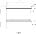
- the display screen is divided into a display region 1 and a non-display region 2 surrounding the display region 1; the display screen includes a first substrate 11 and a second substrate 12 which are disposed opposite to each other, and at least one transparent antenna structure 3 located in the display region 1; the antenna structure 3 is disposed at a side of the second substrate 12 facing away from the first substrate 11, wherein the side of the second substrate 12 facing away from the first substrate 11 is further provided with a touch panel 16, and the antenna structure 3 is disposed between the touch panel 16 and the second substrate 12.
- the touch panel in this kind of structure can be combined with any display screen of Figs. 2 to 8 without repeating herein.
- the display screen is divided into a display region 1 and a non-display region 2 surrounding the display region 1; the display screen includes a first substrate 11 and a second substrate 12 which are disposed opposite to each other, and at least one transparent antenna structure 3 located in the display region 1; a side of the second substrate 12 facing away from the first substrate 11 is further provided with a touch panel 16 and a protection film 17, and the antenna structure 3 is disposed between the touch panel 16 and the protection film 17.
- the side of the first substrate 11 facing the second substrate 12 can always be provided with a display device layer 13; depending on the type of the display screen, the display device layer 13 can be a pixel unit array layer or an OELD layer, and certainly can also be an electrophoresis particle layer; without listing all details herein.
- the display screens of the embodiments illustrated in Figs. 7 and 8 are suitable for a LCD screen, while the display screens of the embodiments illustrated in Figs. 9 and 10 can be combined with the display screens of the embodiments illustrated in Figs. 2 to 8 so as to realize a touch function.
- a liquid crystal (LC) layer (not illustrated) can be disposed between the first substrate 11 and the second substrate 12; and the antenna 31 and the capacitor 32 in each of the display screens illustrated in Figs. 2 to 10 can realize a connection between the display screen and an external circuit through a flexible circuit board, a port device or other connection methods, without illustrating herein.
- LC liquid crystal
- the antenna 31 can have a spiral line shape illustrated in Fig. 1 , or can simply have a line shape, or can have other shapes which can realize receiving or sending signals without repeating herein.
- the transparent antenna structure formed in the display region of the display screen by means of the transparent antenna structure formed in the display region of the display screen, a space sufficient to dispose the antenna can be provided, and the signal of the antenna will not be blocked by a middle metallic layer of the portable device; as a result, the manufacturing process of the antenna of the portable device can be simplified and the manufacturing difficulty can be reduced.
- an embodiment of the present invention further provides a portable device 200 including the display screen 100 according to any of the preceding embodiments.
- the portable device provided by the embodiment of the present invention, by means of the transparent antenna structure formed in the display region of the display screen, a space sufficient to dispose the antenna can be provided, and the signal of the antenna will not be blocked by a middle metallic layer of the portable device; as a result, the manufacturing process of the antenna of the portable device can be simplified and the manufacturing difficulty can be reduced.
Landscapes
- Engineering & Computer Science (AREA)
- Physics & Mathematics (AREA)
- Theoretical Computer Science (AREA)
- Computer Hardware Design (AREA)
- General Engineering & Computer Science (AREA)
- Human Computer Interaction (AREA)
- General Physics & Mathematics (AREA)
- Computer Networks & Wireless Communication (AREA)
- Optics & Photonics (AREA)
- Electromagnetism (AREA)
- Microelectronics & Electronic Packaging (AREA)
- Details Of Aerials (AREA)
- Devices For Indicating Variable Information By Combining Individual Elements (AREA)
- Telephone Set Structure (AREA)
- Support Of Aerials (AREA)
Claims (12)
- Anzeigebildschirm, umfassend:eine Anzeigeregion (1); undeine Nichtanzeigeregion (2), die angeordnet ist, um die Anzeigeregion (1) zu umranden,wobei die Anzeigeregion (1) zumindest eine transparente Antennenstruktur (3) umfasst, wobei die Antennenstruktur (3) eine Antenne (31) und einen Kondensator (32), die in einer gleichen Schicht lokalisiert sind, umfasst, und wobei der Kondensator (32) elektrisch an die Antenne (31) angeschlossen ist,wobei der Anzeigebildschirm außerdem ein erstes Substrat (11) und ein zweites Substrat (12) umfasst, die zueinander gegenüberliegend angeordnet sind, und wobei die Antennenstruktur (3) auf einer Seite des zweiten Substrats (12), die von dem ersten Substrat (11) abgewandt ist, angeordnet ist, wobeieine Seite des zweiten Substrats (21), die von dem ersten Substrat (11) abgewandt ist, außerdem mit einer Berührtafel (16) versehen ist, und die Antennenstruktur (3) zwischen der Berührtafel (16) und dem zweiten Substrat (12) angeordnet ist;oder,wobei eine Seite des zweiten Substrats (12), die von dem ersten Substrat (11) abgewandt ist, außerdem mit einer Berührtafel (16) und einem Schutzfilm (17) versehen ist und die Antennenstruktur (3) zwischen der Berührtafel (16) und dem Schutzfilm (17) angeordnet ist.
- Anzeigebildschirm gemäß Anspruch 1, wobei eine Anzeigevorrichtungsschicht (13) zwischen dem ersten Substrat (11) und der Antennenstruktur (3) angeordnet ist.
- Anzeigebildschirm gemäß Anspruch 2, wobei die Anzeigevorrichtungsschicht (13) eine Pixeleinheit-Array-Schicht ist,
und/ oder
wobei die Anzeigevorrichtungsschicht (13) eine organische Elektrolumineszenz-Anzeige, OLED, Schicht ist. - Anzeigebildschirm gemäß Anspruch 1, wobei eine Seite des zweiten Substrats (12), die dem ersten Substrat zugewandt ist, außerdem mit einer Anzeigefunktionsschicht (14) versehen ist.
- Anzeigebildschirm gemäß Anspruch 4, wobei die Anzeigefunktionsschicht (14) ausgewählt ist aus einer Gruppe bestehend aus einer Farbwiderstandsschicht, einer Schwarzmatrix und einer Abstandsschicht.
- Anzeigebildschirm gemäß Anspruch 1, wobei eine Seite des zweiten Substrats (12), die dem ersten Substrat (11) zugewandt ist, außerdem mit einem Polarisator (15) versehen ist und die Antennenstruktur (3) zwischen dem Polarisator (15) und dem zweiten Substrat (12) angeordnet ist,
oder,
wobei die Seite des zweiten Substrats (12), die dem ersten Substrat zugewandt ist, außerdem mit einem Polarisator (15) versehen ist und der Polarisator zwischen der Antennenstruktur (3) und dem zweiten Substrat (12) angeordnet ist. - Anzeigebildschirm gemäß einem der Ansprüche 1 - 6, außerdem umfassend eine Abschirmstruktur (33), hergestellt aus einem transparenten Isoliermaterial, wobei die Abschirmstruktur (33) über oder unter der Antenne (31) und dem Kondensator (32) angeordnet ist, und wobei vertikale Projektionen der Antenne (31) und des Kondensators (32) in die Anzeigeregion (1) in einen Bereich einer Vertikalprojektion der Abschirmstruktur (33) in die Anzeigeregion (1) fallen.
- Anzeigebildschirm gemäß einem der Ansprüche 1 bis 6, wobei das erste Substrat (11) ein Array-Substrat ist und das zweite Substrat (12) ein Farbfiltersubstrat ist.
- Anzeigebildschirm gemäß Anspruch 1, wobei das erste Substrat (11) ein Array-Substrat ist und das zweite Substrat (12) eine Einkapselungsabdeckplatte ist.
- Anzeigebildschirm gemäß Anspruch 1, wobei Materialien der Antenne (31) und des Kondensators (32) gewählt sind aus einer Gruppe, bestehend aus Indiumzinnoxid, Indiumzinkoxid, Indiumgalliumzinkoxid, Nanometersilberleitungsmaterial, Kohlenstoffröhrenmaterial und Graphenmaterial.
- Anzeigebildschirm gemäß Anspruch 1, wobei die Antenne (31) gewählt ist aus einer Gruppe, bestehend aus Nahfeldkommunikation, NFC, -antennen, Bluetooth-Antennen, Globalpositionssystem, GPS,-Antennen, BeiDou-Navigationssatellitensystem, BDS,-Antennen, Radiofrequenz, RF,-Antennen und Frequenzmodulations, FM,-Antennen.
- Tragbare Vorrichtung, umfassend einen Anzeigebildschirm gemäß einem der Ansprüche 1 - 11.
Applications Claiming Priority (2)
| Application Number | Priority Date | Filing Date | Title |
|---|---|---|---|
| CN201510451123.1A CN105094231B (zh) | 2015-07-28 | 2015-07-28 | 一种显示屏和便携设备 |
| PCT/CN2016/072825 WO2017016208A1 (zh) | 2015-07-28 | 2016-01-29 | 显示屏和便携设备 |
Publications (3)
| Publication Number | Publication Date |
|---|---|
| EP3330831A1 EP3330831A1 (de) | 2018-06-06 |
| EP3330831A4 EP3330831A4 (de) | 2019-04-03 |
| EP3330831B1 true EP3330831B1 (de) | 2021-08-25 |
Family
ID=54574885
Family Applications (1)
| Application Number | Title | Priority Date | Filing Date |
|---|---|---|---|
| EP16763188.6A Active EP3330831B1 (de) | 2015-07-28 | 2016-01-29 | Bildschirm und tragbare vorrichtung |
Country Status (4)
| Country | Link |
|---|---|
| US (1) | US9954268B2 (de) |
| EP (1) | EP3330831B1 (de) |
| CN (1) | CN105094231B (de) |
| WO (1) | WO2017016208A1 (de) |
Families Citing this family (24)
| Publication number | Priority date | Publication date | Assignee | Title |
|---|---|---|---|---|
| CN105094231B (zh) * | 2015-07-28 | 2019-03-01 | 京东方科技集团股份有限公司 | 一种显示屏和便携设备 |
| JP6560610B2 (ja) * | 2015-12-18 | 2019-08-14 | 株式会社ジャパンディスプレイ | 表示装置 |
| US10482810B2 (en) * | 2016-03-08 | 2019-11-19 | Dell Products L.P. | Integrated folded OLED display in an information handling system portable housing for disabling pixels based upon antenna activity |
| WO2017152780A1 (zh) * | 2016-03-10 | 2017-09-14 | 昆山维信诺科技有限公司 | 具有nfc通信功能的显示装置 |
| KR102666192B1 (ko) * | 2016-07-28 | 2024-05-14 | 삼성디스플레이 주식회사 | 표시 장치 |
| CN106229626A (zh) * | 2016-09-12 | 2016-12-14 | 深圳市金诺和信通讯有限公司 | 具有天线功能的透明面板、显示屏组件及无线通信设备 |
| US10211520B2 (en) * | 2016-10-11 | 2019-02-19 | Motorola Mobility Llc | Electronic device with transparent antenna |
| CN106299627B (zh) * | 2016-10-18 | 2023-06-02 | 京东方科技集团股份有限公司 | 一种液晶天线及通信设备 |
| CN106941206B (zh) * | 2017-03-29 | 2019-12-31 | 盐池县荣桂昌食品科技有限公司 | 电子装置及其制备方法 |
| CN106842672B (zh) * | 2017-04-19 | 2019-07-26 | 京东方科技集团股份有限公司 | 一种显示装置 |
| CN106932947B (zh) | 2017-05-16 | 2020-04-17 | 京东方科技集团股份有限公司 | 阵列基板、显示面板和人机交互终端 |
| EP3624261B1 (de) * | 2017-06-23 | 2021-08-25 | Mitsubishi Electric Corporation | Antennenvorrichtung |
| WO2019056581A1 (en) * | 2017-09-25 | 2019-03-28 | Antwave Intellectual Property Limited | SYSTEMS, APPARATUS AND METHODS FOR IMPROVING PERFORMANCE OF ANTENNA IN ELECTRONIC DEVICES |
| CN108512959B (zh) * | 2018-03-28 | 2020-08-14 | Oppo广东移动通信有限公司 | 电子设备及存储介质 |
| CN108881527A (zh) * | 2018-05-23 | 2018-11-23 | 深圳市海德门电子有限公司 | 屏幕、设备、屏幕的制备方法 |
| CN108711669B (zh) * | 2018-05-28 | 2021-04-23 | 京东方科技集团股份有限公司 | 一种频率可调天线及其制作方法 |
| US20200192542A1 (en) * | 2018-12-12 | 2020-06-18 | Novatek Microelectronics Corp. | Display device with integrated antenna and method thereof |
| CN111614801A (zh) * | 2019-02-25 | 2020-09-01 | Oppo广东移动通信有限公司 | 显示屏组件和电子设备 |
| CN110444857B (zh) | 2019-08-05 | 2021-07-23 | 维沃移动通信有限公司 | 一种终端设备 |
| CN111029724B (zh) * | 2019-12-24 | 2021-03-05 | Oppo广东移动通信有限公司 | 移动终端 |
| CN113258274A (zh) * | 2020-02-10 | 2021-08-13 | 东友精细化工有限公司 | 天线堆叠结构和包括天线堆叠结构的显示装置 |
| CN113745810B (zh) * | 2020-05-28 | 2024-07-23 | 北京小米移动软件有限公司 | 一种功能模组、终端设备和功能模组的制作方法 |
| CN112118337A (zh) * | 2020-09-25 | 2020-12-22 | Oppo(重庆)智能科技有限公司 | 天线控制方法及电子设备 |
| CN114327146B (zh) * | 2021-12-31 | 2023-10-20 | 云谷(固安)科技有限公司 | 显示面板和显示装置 |
Family Cites Families (23)
| Publication number | Priority date | Publication date | Assignee | Title |
|---|---|---|---|---|
| US6522308B1 (en) * | 2000-01-03 | 2003-02-18 | Ask S.A. | Variable capacitance coupling antenna |
| CN1622391A (zh) | 2003-11-28 | 2005-06-01 | 神达电脑股份有限公司 | 无线式液晶显示器天线 |
| DE602004014257D1 (de) | 2004-06-02 | 2008-07-17 | Sony Ericsson Mobile Comm Ab | Transparente leitende Antenne für ein tragbares Kommunikationsgerät |
| WO2006039699A2 (en) * | 2004-10-01 | 2006-04-13 | De Rochemont L Pierre | Ceramic antenna module and methods of manufacture thereof |
| CN101308266B (zh) * | 2008-07-11 | 2010-06-02 | 昆山龙腾光电有限公司 | 液晶显示面板、液晶显示装置和电子设备 |
| WO2010064351A1 (ja) | 2008-12-02 | 2010-06-10 | 三菱電機株式会社 | タッチパネルおよびタッチパネルを備えた電子機器 |
| US20100321325A1 (en) * | 2009-06-17 | 2010-12-23 | Springer Gregory A | Touch and display panel antennas |
| KR20120072220A (ko) * | 2010-12-23 | 2012-07-03 | 한국전자통신연구원 | 터치입력장치 및 이를 이용한 전자기파 송수신 장치 |
| KR20130070247A (ko) | 2011-12-19 | 2013-06-27 | 엘지전자 주식회사 | 터치 패널 및 이를 포함하는 이동 단말기 |
| CN102737582B (zh) | 2012-04-06 | 2014-07-09 | 信利工业(汕尾)有限公司 | 一种集成NFC天线的TP On/In Cell型有机电致发光显示器 |
| US10003121B2 (en) * | 2012-08-29 | 2018-06-19 | Htc Corporation | Mobile device and antenna structure |
| KR102013588B1 (ko) * | 2012-09-19 | 2019-08-23 | 엘지전자 주식회사 | 이동 단말기 |
| US20140104157A1 (en) | 2012-10-15 | 2014-04-17 | Qualcomm Mems Technologies, Inc. | Transparent antennas on a display device |
| US9287612B2 (en) * | 2012-11-16 | 2016-03-15 | Sony Mobile Communications Ab | Transparent antennas for wireless terminals |
| US8941095B2 (en) * | 2012-12-06 | 2015-01-27 | Hrl Laboratories, Llc | Methods for integrating and forming optically transparent devices on surfaces |
| CN103905095B (zh) * | 2012-12-28 | 2016-03-02 | 联想(北京)有限公司 | 电子设备和用于布置近距离通信天线的方法 |
| CN203397335U (zh) * | 2013-05-22 | 2014-01-15 | 深圳市金立通信设备有限公司 | 一种输入/输出装置及终端 |
| US9660344B2 (en) * | 2013-07-23 | 2017-05-23 | Intel Corporation | Optically transparent antenna for wireless communication and energy transfer |
| CN203720722U (zh) * | 2014-01-30 | 2014-07-16 | 宇龙计算机通信科技(深圳)有限公司 | 一种集成天线功能的显示屏及应用该显示屏的终端设备 |
| CN206727211U (zh) * | 2014-03-28 | 2017-12-08 | 株式会社村田制作所 | 天线装置以及通信设备 |
| US9553352B2 (en) * | 2014-09-26 | 2017-01-24 | Intel Corporation | Communication device and display incorporating antennas between display pixels |
| KR102399741B1 (ko) * | 2015-05-22 | 2022-05-20 | 삼성전자주식회사 | 디스플레이 모듈 및 그 제조 방법 |
| CN105094231B (zh) * | 2015-07-28 | 2019-03-01 | 京东方科技集团股份有限公司 | 一种显示屏和便携设备 |
-
2015
- 2015-07-28 CN CN201510451123.1A patent/CN105094231B/zh active Active
-
2016
- 2016-01-29 WO PCT/CN2016/072825 patent/WO2017016208A1/zh active Application Filing
- 2016-01-29 US US15/127,724 patent/US9954268B2/en active Active
- 2016-01-29 EP EP16763188.6A patent/EP3330831B1/de active Active
Also Published As
| Publication number | Publication date |
|---|---|
| US20170179567A1 (en) | 2017-06-22 |
| CN105094231A (zh) | 2015-11-25 |
| US9954268B2 (en) | 2018-04-24 |
| CN105094231B (zh) | 2019-03-01 |
| WO2017016208A1 (zh) | 2017-02-02 |
| EP3330831A4 (de) | 2019-04-03 |
| EP3330831A1 (de) | 2018-06-06 |
Similar Documents
| Publication | Publication Date | Title |
|---|---|---|
| EP3330831B1 (de) | Bildschirm und tragbare vorrichtung | |
| US11894600B2 (en) | Electronic device with near-field antenna operating through display | |
| US9131037B2 (en) | Electronic device with conductive fabric shield wall | |
| EP2774215B1 (de) | Antenne mit gefaltetem monopol und schleifenmoden | |
| CN207074710U (zh) | 电子设备 | |
| EP2786444B1 (de) | Antenne mit schaltbarem induktor mit low-band-abstimmung | |
| CN102594389B (zh) | 用于降低电子设备中的射频干扰的谐振元件 | |
| US9178268B2 (en) | Antennas integrated with speakers and methods for suppressing cavity modes | |
| CN109216868B (zh) | 天线组件及电子设备 | |
| CN108736134B (zh) | 天线组件及电子设备 | |
| CN108232473B (zh) | 天线组件、电子设备及天线切换方法 | |
| CN109346828A (zh) | 天线组件及电子设备 | |
| CN112448132B (zh) | 穿戴式电子设备 | |
| CN107492716A (zh) | 控制方法、天线装置及电子设备 | |
| CN113067147A (zh) | 天线组件及电子设备 | |
| CN111613877A (zh) | 一种天线结构及移动终端 | |
| CN108461895B (zh) | 天线组件、电子设备及天线切换方法 | |
| CN112448133A (zh) | 穿戴式电子设备 | |
| CN112886178A (zh) | 穿戴式电子设备 | |
| CN212571326U (zh) | 天线组件及电子设备 | |
| CN218448435U (zh) | 天线组件及电子设备 | |
| CN112886243A (zh) | 穿戴式电子设备 | |
| KR102098144B1 (ko) | 터치 윈도우 및 이를 포함하는 디스플레이 |
Legal Events
| Date | Code | Title | Description |
|---|---|---|---|
| STAA | Information on the status of an ep patent application or granted ep patent |
Free format text: STATUS: THE INTERNATIONAL PUBLICATION HAS BEEN MADE |
|
| PUAI | Public reference made under article 153(3) epc to a published international application that has entered the european phase |
Free format text: ORIGINAL CODE: 0009012 |
|
| STAA | Information on the status of an ep patent application or granted ep patent |
Free format text: STATUS: REQUEST FOR EXAMINATION WAS MADE |
|
| 17P | Request for examination filed |
Effective date: 20160920 |
|
| AK | Designated contracting states |
Kind code of ref document: A1 Designated state(s): AL AT BE BG CH CY CZ DE DK EE ES FI FR GB GR HR HU IE IS IT LI LT LU LV MC MK MT NL NO PL PT RO RS SE SI SK SM TR |
|
| AX | Request for extension of the european patent |
Extension state: BA ME |
|
| DAV | Request for validation of the european patent (deleted) | ||
| DAX | Request for extension of the european patent (deleted) | ||
| A4 | Supplementary search report drawn up and despatched |
Effective date: 20190228 |
|
| RIC1 | Information provided on ipc code assigned before grant |
Ipc: H01Q 21/24 20060101ALI20190222BHEP Ipc: H01Q 1/24 20060101ALI20190222BHEP Ipc: G06F 1/16 20060101AFI20190222BHEP Ipc: H01Q 21/28 20060101ALI20190222BHEP Ipc: H01Q 1/22 20060101ALI20190222BHEP Ipc: H01Q 1/36 20060101ALI20190222BHEP Ipc: H01Q 1/38 20060101ALI20190222BHEP Ipc: H01Q 1/52 20060101ALI20190222BHEP |
|
| GRAP | Despatch of communication of intention to grant a patent |
Free format text: ORIGINAL CODE: EPIDOSNIGR1 |
|
| STAA | Information on the status of an ep patent application or granted ep patent |
Free format text: STATUS: GRANT OF PATENT IS INTENDED |
|
| RIC1 | Information provided on ipc code assigned before grant |
Ipc: H01Q 1/24 20060101ALI20210225BHEP Ipc: H01Q 1/52 20060101ALI20210225BHEP Ipc: H01Q 1/38 20060101ALI20210225BHEP Ipc: H01L 51/52 20060101ALN20210225BHEP Ipc: H01Q 1/22 20060101ALI20210225BHEP Ipc: H01Q 1/36 20060101ALI20210225BHEP Ipc: H01Q 21/28 20060101ALI20210225BHEP Ipc: H01L 27/32 20060101ALI20210225BHEP Ipc: G06F 1/16 20060101AFI20210225BHEP |
|
| RIC1 | Information provided on ipc code assigned before grant |
Ipc: H01L 51/52 20060101ALN20210303BHEP Ipc: H01Q 1/36 20060101ALI20210303BHEP Ipc: H01Q 1/22 20060101ALI20210303BHEP Ipc: H01Q 1/38 20060101ALI20210303BHEP Ipc: H01L 27/32 20060101ALI20210303BHEP Ipc: H01Q 1/24 20060101ALI20210303BHEP Ipc: H01Q 21/28 20060101ALI20210303BHEP Ipc: H01Q 1/52 20060101ALI20210303BHEP Ipc: G06F 1/16 20060101AFI20210303BHEP |
|
| INTG | Intention to grant announced |
Effective date: 20210316 |
|
| RIC1 | Information provided on ipc code assigned before grant |
Ipc: H01L 51/52 20060101ALN20210305BHEP Ipc: H01L 27/32 20060101ALI20210305BHEP Ipc: H01Q 1/38 20060101ALI20210305BHEP Ipc: H01Q 1/36 20060101ALI20210305BHEP Ipc: H01Q 1/52 20060101ALI20210305BHEP Ipc: H01Q 21/28 20060101ALI20210305BHEP Ipc: H01Q 1/22 20060101ALI20210305BHEP Ipc: H01Q 1/24 20060101ALI20210305BHEP Ipc: G06F 1/16 20060101AFI20210305BHEP |
|
| GRAS | Grant fee paid |
Free format text: ORIGINAL CODE: EPIDOSNIGR3 |
|
| GRAA | (expected) grant |
Free format text: ORIGINAL CODE: 0009210 |
|
| STAA | Information on the status of an ep patent application or granted ep patent |
Free format text: STATUS: THE PATENT HAS BEEN GRANTED |
|
| AK | Designated contracting states |
Kind code of ref document: B1 Designated state(s): AL AT BE BG CH CY CZ DE DK EE ES FI FR GB GR HR HU IE IS IT LI LT LU LV MC MK MT NL NO PL PT RO RS SE SI SK SM TR |
|
| REG | Reference to a national code |
Ref country code: CH Ref legal event code: EP |
|
| REG | Reference to a national code |
Ref country code: IE Ref legal event code: FG4D Ref country code: AT Ref legal event code: REF Ref document number: 1424460 Country of ref document: AT Kind code of ref document: T Effective date: 20210915 |
|
| REG | Reference to a national code |
Ref country code: DE Ref legal event code: R096 Ref document number: 602016062752 Country of ref document: DE |
|
| REG | Reference to a national code |
Ref country code: NL Ref legal event code: FP |
|
| REG | Reference to a national code |
Ref country code: LT Ref legal event code: MG9D |
|
| REG | Reference to a national code |
Ref country code: AT Ref legal event code: MK05 Ref document number: 1424460 Country of ref document: AT Kind code of ref document: T Effective date: 20210825 |
|
| PG25 | Lapsed in a contracting state [announced via postgrant information from national office to epo] |
Ref country code: LT Free format text: LAPSE BECAUSE OF FAILURE TO SUBMIT A TRANSLATION OF THE DESCRIPTION OR TO PAY THE FEE WITHIN THE PRESCRIBED TIME-LIMIT Effective date: 20210825 Ref country code: AT Free format text: LAPSE BECAUSE OF FAILURE TO SUBMIT A TRANSLATION OF THE DESCRIPTION OR TO PAY THE FEE WITHIN THE PRESCRIBED TIME-LIMIT Effective date: 20210825 Ref country code: BG Free format text: LAPSE BECAUSE OF FAILURE TO SUBMIT A TRANSLATION OF THE DESCRIPTION OR TO PAY THE FEE WITHIN THE PRESCRIBED TIME-LIMIT Effective date: 20211125 Ref country code: NO Free format text: LAPSE BECAUSE OF FAILURE TO SUBMIT A TRANSLATION OF THE DESCRIPTION OR TO PAY THE FEE WITHIN THE PRESCRIBED TIME-LIMIT Effective date: 20211125 Ref country code: PT Free format text: LAPSE BECAUSE OF FAILURE TO SUBMIT A TRANSLATION OF THE DESCRIPTION OR TO PAY THE FEE WITHIN THE PRESCRIBED TIME-LIMIT Effective date: 20211227 Ref country code: HR Free format text: LAPSE BECAUSE OF FAILURE TO SUBMIT A TRANSLATION OF THE DESCRIPTION OR TO PAY THE FEE WITHIN THE PRESCRIBED TIME-LIMIT Effective date: 20210825 Ref country code: FI Free format text: LAPSE BECAUSE OF FAILURE TO SUBMIT A TRANSLATION OF THE DESCRIPTION OR TO PAY THE FEE WITHIN THE PRESCRIBED TIME-LIMIT Effective date: 20210825 Ref country code: ES Free format text: LAPSE BECAUSE OF FAILURE TO SUBMIT A TRANSLATION OF THE DESCRIPTION OR TO PAY THE FEE WITHIN THE PRESCRIBED TIME-LIMIT Effective date: 20210825 Ref country code: RS Free format text: LAPSE BECAUSE OF FAILURE TO SUBMIT A TRANSLATION OF THE DESCRIPTION OR TO PAY THE FEE WITHIN THE PRESCRIBED TIME-LIMIT Effective date: 20210825 Ref country code: SE Free format text: LAPSE BECAUSE OF FAILURE TO SUBMIT A TRANSLATION OF THE DESCRIPTION OR TO PAY THE FEE WITHIN THE PRESCRIBED TIME-LIMIT Effective date: 20210825 |
|
| PG25 | Lapsed in a contracting state [announced via postgrant information from national office to epo] |
Ref country code: PL Free format text: LAPSE BECAUSE OF FAILURE TO SUBMIT A TRANSLATION OF THE DESCRIPTION OR TO PAY THE FEE WITHIN THE PRESCRIBED TIME-LIMIT Effective date: 20210825 Ref country code: LV Free format text: LAPSE BECAUSE OF FAILURE TO SUBMIT A TRANSLATION OF THE DESCRIPTION OR TO PAY THE FEE WITHIN THE PRESCRIBED TIME-LIMIT Effective date: 20210825 Ref country code: GR Free format text: LAPSE BECAUSE OF FAILURE TO SUBMIT A TRANSLATION OF THE DESCRIPTION OR TO PAY THE FEE WITHIN THE PRESCRIBED TIME-LIMIT Effective date: 20211126 |
|
| PG25 | Lapsed in a contracting state [announced via postgrant information from national office to epo] |
Ref country code: DK Free format text: LAPSE BECAUSE OF FAILURE TO SUBMIT A TRANSLATION OF THE DESCRIPTION OR TO PAY THE FEE WITHIN THE PRESCRIBED TIME-LIMIT Effective date: 20210825 |
|
| REG | Reference to a national code |
Ref country code: DE Ref legal event code: R097 Ref document number: 602016062752 Country of ref document: DE |
|
| PG25 | Lapsed in a contracting state [announced via postgrant information from national office to epo] |
Ref country code: SM Free format text: LAPSE BECAUSE OF FAILURE TO SUBMIT A TRANSLATION OF THE DESCRIPTION OR TO PAY THE FEE WITHIN THE PRESCRIBED TIME-LIMIT Effective date: 20210825 Ref country code: SK Free format text: LAPSE BECAUSE OF FAILURE TO SUBMIT A TRANSLATION OF THE DESCRIPTION OR TO PAY THE FEE WITHIN THE PRESCRIBED TIME-LIMIT Effective date: 20210825 Ref country code: RO Free format text: LAPSE BECAUSE OF FAILURE TO SUBMIT A TRANSLATION OF THE DESCRIPTION OR TO PAY THE FEE WITHIN THE PRESCRIBED TIME-LIMIT Effective date: 20210825 Ref country code: EE Free format text: LAPSE BECAUSE OF FAILURE TO SUBMIT A TRANSLATION OF THE DESCRIPTION OR TO PAY THE FEE WITHIN THE PRESCRIBED TIME-LIMIT Effective date: 20210825 Ref country code: CZ Free format text: LAPSE BECAUSE OF FAILURE TO SUBMIT A TRANSLATION OF THE DESCRIPTION OR TO PAY THE FEE WITHIN THE PRESCRIBED TIME-LIMIT Effective date: 20210825 Ref country code: AL Free format text: LAPSE BECAUSE OF FAILURE TO SUBMIT A TRANSLATION OF THE DESCRIPTION OR TO PAY THE FEE WITHIN THE PRESCRIBED TIME-LIMIT Effective date: 20210825 |
|
| PLBE | No opposition filed within time limit |
Free format text: ORIGINAL CODE: 0009261 |
|
| STAA | Information on the status of an ep patent application or granted ep patent |
Free format text: STATUS: NO OPPOSITION FILED WITHIN TIME LIMIT |
|
| PG25 | Lapsed in a contracting state [announced via postgrant information from national office to epo] |
Ref country code: IT Free format text: LAPSE BECAUSE OF FAILURE TO SUBMIT A TRANSLATION OF THE DESCRIPTION OR TO PAY THE FEE WITHIN THE PRESCRIBED TIME-LIMIT Effective date: 20210825 |
|
| 26N | No opposition filed |
Effective date: 20220527 |
|
| PG25 | Lapsed in a contracting state [announced via postgrant information from national office to epo] |
Ref country code: SI Free format text: LAPSE BECAUSE OF FAILURE TO SUBMIT A TRANSLATION OF THE DESCRIPTION OR TO PAY THE FEE WITHIN THE PRESCRIBED TIME-LIMIT Effective date: 20210825 Ref country code: MC Free format text: LAPSE BECAUSE OF FAILURE TO SUBMIT A TRANSLATION OF THE DESCRIPTION OR TO PAY THE FEE WITHIN THE PRESCRIBED TIME-LIMIT Effective date: 20210825 |
|
| REG | Reference to a national code |
Ref country code: CH Ref legal event code: PL |
|
| REG | Reference to a national code |
Ref country code: BE Ref legal event code: MM Effective date: 20220131 |
|
| PG25 | Lapsed in a contracting state [announced via postgrant information from national office to epo] |
Ref country code: LU Free format text: LAPSE BECAUSE OF NON-PAYMENT OF DUE FEES Effective date: 20220129 |
|
| PG25 | Lapsed in a contracting state [announced via postgrant information from national office to epo] |
Ref country code: BE Free format text: LAPSE BECAUSE OF NON-PAYMENT OF DUE FEES Effective date: 20220131 |
|
| PG25 | Lapsed in a contracting state [announced via postgrant information from national office to epo] |
Ref country code: LI Free format text: LAPSE BECAUSE OF NON-PAYMENT OF DUE FEES Effective date: 20220131 Ref country code: CH Free format text: LAPSE BECAUSE OF NON-PAYMENT OF DUE FEES Effective date: 20220131 |
|
| PG25 | Lapsed in a contracting state [announced via postgrant information from national office to epo] |
Ref country code: IE Free format text: LAPSE BECAUSE OF NON-PAYMENT OF DUE FEES Effective date: 20220129 |
|
| PGFP | Annual fee paid to national office [announced via postgrant information from national office to epo] |
Ref country code: NL Payment date: 20240119 Year of fee payment: 9 |
|
| PG25 | Lapsed in a contracting state [announced via postgrant information from national office to epo] |
Ref country code: HU Free format text: LAPSE BECAUSE OF FAILURE TO SUBMIT A TRANSLATION OF THE DESCRIPTION OR TO PAY THE FEE WITHIN THE PRESCRIBED TIME-LIMIT; INVALID AB INITIO Effective date: 20160129 |
|
| PG25 | Lapsed in a contracting state [announced via postgrant information from national office to epo] |
Ref country code: MK Free format text: LAPSE BECAUSE OF FAILURE TO SUBMIT A TRANSLATION OF THE DESCRIPTION OR TO PAY THE FEE WITHIN THE PRESCRIBED TIME-LIMIT Effective date: 20210825 Ref country code: CY Free format text: LAPSE BECAUSE OF FAILURE TO SUBMIT A TRANSLATION OF THE DESCRIPTION OR TO PAY THE FEE WITHIN THE PRESCRIBED TIME-LIMIT Effective date: 20210825 |
|
| PGFP | Annual fee paid to national office [announced via postgrant information from national office to epo] |
Ref country code: DE Payment date: 20240119 Year of fee payment: 9 Ref country code: GB Payment date: 20240119 Year of fee payment: 9 |
|
| PGFP | Annual fee paid to national office [announced via postgrant information from national office to epo] |
Ref country code: FR Payment date: 20240124 Year of fee payment: 9 |
|
| PG25 | Lapsed in a contracting state [announced via postgrant information from national office to epo] |
Ref country code: TR Free format text: LAPSE BECAUSE OF FAILURE TO SUBMIT A TRANSLATION OF THE DESCRIPTION OR TO PAY THE FEE WITHIN THE PRESCRIBED TIME-LIMIT Effective date: 20210825 |