EP3330036B1 - Pyromètre pour système de recuit au laser compatible avec une couche d'absorbeur optique de carbone amorphe - Google Patents
Pyromètre pour système de recuit au laser compatible avec une couche d'absorbeur optique de carbone amorphe Download PDFInfo
- Publication number
- EP3330036B1 EP3330036B1 EP18152336.6A EP18152336A EP3330036B1 EP 3330036 B1 EP3330036 B1 EP 3330036B1 EP 18152336 A EP18152336 A EP 18152336A EP 3330036 B1 EP3330036 B1 EP 3330036B1
- Authority
- EP
- European Patent Office
- Prior art keywords
- wavelength
- pyrometer
- laser
- filter
- substrate
- Prior art date
- Legal status (The legal status is an assumption and is not a legal conclusion. Google has not performed a legal analysis and makes no representation as to the accuracy of the status listed.)
- Active
Links
- 230000003287 optical effect Effects 0.000 title claims description 60
- 229910003481 amorphous carbon Inorganic materials 0.000 title claims description 29
- 239000006096 absorbing agent Substances 0.000 title claims description 12
- 238000005224 laser annealing Methods 0.000 title claims description 8
- 230000005855 radiation Effects 0.000 claims description 62
- 239000000758 substrate Substances 0.000 claims description 40
- 230000007704 transition Effects 0.000 claims description 34
- 230000004044 response Effects 0.000 claims description 28
- 238000010521 absorption reaction Methods 0.000 claims description 19
- 230000000903 blocking effect Effects 0.000 claims description 14
- 239000000463 material Substances 0.000 claims description 14
- 238000000034 method Methods 0.000 claims description 10
- 238000012545 processing Methods 0.000 claims description 10
- 238000000576 coating method Methods 0.000 claims description 6
- VYPSYNLAJGMNEJ-UHFFFAOYSA-N silicon dioxide Inorganic materials O=[Si]=O VYPSYNLAJGMNEJ-UHFFFAOYSA-N 0.000 claims description 4
- 239000002194 amorphous carbon material Substances 0.000 claims description 3
- 239000010453 quartz Substances 0.000 claims description 3
- 239000011248 coating agent Substances 0.000 claims description 2
- 238000003384 imaging method Methods 0.000 claims description 2
- 235000012431 wafers Nutrition 0.000 description 41
- 239000010410 layer Substances 0.000 description 38
- 230000008033 biological extinction Effects 0.000 description 10
- 230000010287 polarization Effects 0.000 description 9
- 230000005457 Black-body radiation Effects 0.000 description 6
- 238000000137 annealing Methods 0.000 description 5
- 238000013459 approach Methods 0.000 description 4
- 230000005540 biological transmission Effects 0.000 description 4
- 238000009529 body temperature measurement Methods 0.000 description 4
- 238000001914 filtration Methods 0.000 description 4
- 239000004065 semiconductor Substances 0.000 description 4
- 238000001228 spectrum Methods 0.000 description 4
- 230000002269 spontaneous effect Effects 0.000 description 4
- 229910001218 Gallium arsenide Inorganic materials 0.000 description 3
- XUIMIQQOPSSXEZ-UHFFFAOYSA-N Silicon Chemical compound [Si] XUIMIQQOPSSXEZ-UHFFFAOYSA-N 0.000 description 3
- 229910052710 silicon Inorganic materials 0.000 description 3
- 239000010703 silicon Substances 0.000 description 3
- 239000010409 thin film Substances 0.000 description 3
- 239000002019 doping agent Substances 0.000 description 2
- 230000004907 flux Effects 0.000 description 2
- 238000010438 heat treatment Methods 0.000 description 2
- 230000007246 mechanism Effects 0.000 description 2
- 230000008569 process Effects 0.000 description 2
- 238000011160 research Methods 0.000 description 2
- 239000002344 surface layer Substances 0.000 description 2
- 239000004593 Epoxy Substances 0.000 description 1
- 238000004616 Pyrometry Methods 0.000 description 1
- 239000005083 Zinc sulfide Substances 0.000 description 1
- 230000004913 activation Effects 0.000 description 1
- 230000001154 acute effect Effects 0.000 description 1
- 239000000853 adhesive Substances 0.000 description 1
- 230000001070 adhesive effect Effects 0.000 description 1
- 238000003491 array Methods 0.000 description 1
- 238000005229 chemical vapour deposition Methods 0.000 description 1
- 238000001816 cooling Methods 0.000 description 1
- 229910001610 cryolite Inorganic materials 0.000 description 1
- 238000002425 crystallisation Methods 0.000 description 1
- 230000008025 crystallization Effects 0.000 description 1
- 230000001066 destructive effect Effects 0.000 description 1
- 238000010586 diagram Methods 0.000 description 1
- 239000003989 dielectric material Substances 0.000 description 1
- 230000000694 effects Effects 0.000 description 1
- 239000008393 encapsulating agent Substances 0.000 description 1
- 238000011049 filling Methods 0.000 description 1
- 239000010408 film Substances 0.000 description 1
- 239000005350 fused silica glass Substances 0.000 description 1
- 239000011521 glass Substances 0.000 description 1
- 239000007943 implant Substances 0.000 description 1
- 230000006872 improvement Effects 0.000 description 1
- 238000004519 manufacturing process Methods 0.000 description 1
- 238000005259 measurement Methods 0.000 description 1
- 239000005304 optical glass Substances 0.000 description 1
- 230000003647 oxidation Effects 0.000 description 1
- 238000007254 oxidation reaction Methods 0.000 description 1
- 238000002310 reflectometry Methods 0.000 description 1
- 125000006850 spacer group Chemical group 0.000 description 1
- 238000002834 transmittance Methods 0.000 description 1
- XLYOFNOQVPJJNP-UHFFFAOYSA-N water Substances O XLYOFNOQVPJJNP-UHFFFAOYSA-N 0.000 description 1
- 229910052984 zinc sulfide Inorganic materials 0.000 description 1
- DRDVZXDWVBGGMH-UHFFFAOYSA-N zinc;sulfide Chemical compound [S-2].[Zn+2] DRDVZXDWVBGGMH-UHFFFAOYSA-N 0.000 description 1
Images


Classifications
-
- B—PERFORMING OPERATIONS; TRANSPORTING
- B23—MACHINE TOOLS; METAL-WORKING NOT OTHERWISE PROVIDED FOR
- B23K—SOLDERING OR UNSOLDERING; WELDING; CLADDING OR PLATING BY SOLDERING OR WELDING; CUTTING BY APPLYING HEAT LOCALLY, e.g. FLAME CUTTING; WORKING BY LASER BEAM
- B23K26/00—Working by laser beam, e.g. welding, cutting or boring
- B23K26/02—Positioning or observing the workpiece, e.g. with respect to the point of impact; Aligning, aiming or focusing the laser beam
- B23K26/03—Observing, e.g. monitoring, the workpiece
- B23K26/032—Observing, e.g. monitoring, the workpiece using optical means
-
- B—PERFORMING OPERATIONS; TRANSPORTING
- B23—MACHINE TOOLS; METAL-WORKING NOT OTHERWISE PROVIDED FOR
- B23K—SOLDERING OR UNSOLDERING; WELDING; CLADDING OR PLATING BY SOLDERING OR WELDING; CUTTING BY APPLYING HEAT LOCALLY, e.g. FLAME CUTTING; WORKING BY LASER BEAM
- B23K26/00—Working by laser beam, e.g. welding, cutting or boring
- B23K26/02—Positioning or observing the workpiece, e.g. with respect to the point of impact; Aligning, aiming or focusing the laser beam
- B23K26/03—Observing, e.g. monitoring, the workpiece
- B23K26/034—Observing the temperature of the workpiece
-
- B—PERFORMING OPERATIONS; TRANSPORTING
- B23—MACHINE TOOLS; METAL-WORKING NOT OTHERWISE PROVIDED FOR
- B23K—SOLDERING OR UNSOLDERING; WELDING; CLADDING OR PLATING BY SOLDERING OR WELDING; CUTTING BY APPLYING HEAT LOCALLY, e.g. FLAME CUTTING; WORKING BY LASER BEAM
- B23K26/00—Working by laser beam, e.g. welding, cutting or boring
- B23K26/02—Positioning or observing the workpiece, e.g. with respect to the point of impact; Aligning, aiming or focusing the laser beam
- B23K26/06—Shaping the laser beam, e.g. by masks or multi-focusing
- B23K26/0665—Shaping the laser beam, e.g. by masks or multi-focusing by beam condensation on the workpiece, e.g. for focusing
-
- B—PERFORMING OPERATIONS; TRANSPORTING
- B23—MACHINE TOOLS; METAL-WORKING NOT OTHERWISE PROVIDED FOR
- B23K—SOLDERING OR UNSOLDERING; WELDING; CLADDING OR PLATING BY SOLDERING OR WELDING; CUTTING BY APPLYING HEAT LOCALLY, e.g. FLAME CUTTING; WORKING BY LASER BEAM
- B23K26/00—Working by laser beam, e.g. welding, cutting or boring
- B23K26/18—Working by laser beam, e.g. welding, cutting or boring using absorbing layers on the workpiece, e.g. for marking or protecting purposes
-
- B—PERFORMING OPERATIONS; TRANSPORTING
- B23—MACHINE TOOLS; METAL-WORKING NOT OTHERWISE PROVIDED FOR
- B23K—SOLDERING OR UNSOLDERING; WELDING; CLADDING OR PLATING BY SOLDERING OR WELDING; CUTTING BY APPLYING HEAT LOCALLY, e.g. FLAME CUTTING; WORKING BY LASER BEAM
- B23K2101/00—Articles made by soldering, welding or cutting
- B23K2101/36—Electric or electronic devices
- B23K2101/40—Semiconductor devices
Definitions
- Thermal processing is required in the fabrication of silicon and other semiconductor integrated circuits formed in silicon wafers or other substrates such as glass panels for displays.
- the required temperatures may range from relatively low temperatures of less than 250°C to greater than 1000°, 1200°, or even 1400°C and may be used for a variety of processes such as dopant implant annealing, crystallization, oxidation, nitridation, silicidation, and chemical vapor deposition as well as others.
- the thermal budget may be considered as the total time at high temperatures necessary to achieve the desired processing results (e.g., dopant activation level).
- the time that the wafer needs to stay at the highest temperature can be very short.
- Rapid thermal processing uses radiant lamps which can be very quickly turned on and off to heat only the wafer and not the rest of the chamber. Pulsed laser annealing using very short (about 20ns) laser pulses is effective at heating only the surface layer and not the underlying wafer, thus allowing very short ramp up and ramp down rates.
- Jennings and Markle versions use CW diode lasers to produce very intense beams of light that strikes the wafer as a thin long line of radiation.
- the line is then scanned over the surface of the wafer in a direction perpendicular to the long dimension of the line beam.
- WO 2006/055130 A2 describes multiple band pass filtering for pyrometry in laser based annealing systems.
- Laser radiation at about 810 nm is produced in an optical system from two laser bar stacks.
- Interleaved beams are input to a polarization multiplexer having a structure of a double polarization beam splitter.
- First and second diagonal interface layers cause the two sets of interleaved beams to be reflected along a common axis from their front faces.
- a source beam is passed through a set of cylindrical lenses to focus the source beam. Further anamorphic lens set or optics are described. The same optics used to focus the laser source light on the wafer is used to direct thermal radiation emitted from the neighborhood of the line beam on the wafer in the reverse direction to a pyrometer.
- a thermal processing system includes a source of laser radiation emitting at a laser wavelength, a beam splitting reflective member arranged to receive the laser radiation, and beam projection optics disposed between one side of the reflective member and a substrate support capable of holding a substrate to be processed.
- a projection optical path for the laser radiation extends from the reflecting member, through the projection optics and toward the substrate support.
- the system further includes a pyrometer on an opposite side of the reflective member and responsive to a pyrometer wavelength range or response band, and a pyrometer optical path extending through the reflective member and to the pyrometer.
- An amorphous carbon optical absorber layer covers the surface of the substrate being processed.
- the system further includes a pyrometer passband filter in the pyrometer optical path having a narrow passband lying in a wavelength window between the laser emission band and an emission band of fluorescence of the optical components of the projection and pyrometer optical paths.
- the pyrometer passband filter blocks the fluorescence emission from the pyrometer optical path.
- the narrow pyrometer filter passband window lies in a wavelength range within which the amorphous carbon layer has a substantial extinction coefficient on the order of or exceeding that of the underlying integrated circuit features.
- a multiple thin film razor edge filter in the pyrometer optical path blocks the laser emission band from the pyrometer optical path.
- the source of laser radiation includes an array of laser emitters.
- the beam projection optics projects a line beam of radiation of the laser wavelength onto a substrate plane over the substrate support, and the system further includes a line beam scanning apparatus having a fast axis transverse to the line beam.
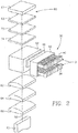
- a gantry structure 10 for two-dimensional scanning includes a pair of fixed parallel rails 12, 14.
- Two parallel gantry beams 16, 18 are fixed together a set distance apart and supported on the fixed rails 12, 14 and are controlled by an unillustrated motor and drive mechanism to slide on rollers or ball bearings together along the fixed rails 12, 14.
- a beam source 20 is slidably supported on the gantry beams 16, 18, and may be suspended below the beams 16, 18 which are controlled by unillustrated motors and drive mechanisms to slide along them.
- a substrate 22 to be processed which may be a silicon wafer 22 for example, is stationarily supported below the gantry structure 10.
- the beam source 20 includes a laser light source and optics to produce a downwardly directed fan-shaped beam 24 that strikes the wafer 22 as a line beam 26 extending generally parallel to the fixed rails 12, 14, in what is conveniently called the slow direction.
- the gantry structure further includes a Z-axis stage for moving the laser light source and optics in a direction generally parallel to the fan-shaped beam 24 to thereby controllably vary the distance between the beam source 20 and the wafer 22 and thus control the focusing of the line beam 26 on the wafer 22.
- Exemplary dimensions of the line beam 26 include a length of 1 cm and a width of 66 microns with an exemplary power density of 220kW/cm 2 .
- the beam source and associated optics may be stationary while the wafer is supported on a stage which scans it in two dimensions.
- the gantry beams 16, 18 are set at a particular position along the fixed rails 12, 14 and the beam source 20 is moved at a uniform speed along the gantry beams 16, 18 to scan the line beam 26 perpendicularly to its long dimension in a direction conveniently called the fast direction.
- the line beam 26 is thereby scanned from one side of the wafer 22 to the other to irradiate a 1 cm swath of the wafer 22.
- the line beam 26 is narrow enough and the scanning speed in the fast direction fast enough that a particular area of the wafer is only momentarily exposed to the optical radiation of the line beam 26 but the intensity at the peak of the line beam is enough to heat the surface region to very high temperatures.
- the deeper portions of the wafer 22 are not significantly heated and further act as a heat sink to quickly cool the surface region.
- the gantry beams 16, 18 are moved along the fixed rails 12, 14 to a new position such that the line beam 26 is moved along its long dimension extending along the slow axis.
- the fast scanning is then performed to irradiate a neighboring swath of the wafer 22.
- the alternating fast and slow scanning are repeated, perhaps in a serpentine path of the beam source 20, until the entire wafer 22 has been thermally processed.
- the optics beam source 20 includes an array of lasers.
- An example is orthographically illustrated in FIGS. 2 , 3 and 5 , in which laser radiation at about 810 nm is produced in an optical system 30 from two laser bar stacks 32, one of which is illustrated in end plan view in FIG. 4 .
- Each laser bar stack 32 includes a number of (e.g., fourteen) parallel bars 34, generally corresponding to a vertical p-n junction in a GaAs semiconductor structure, extending laterally about 1 cm and separated by about 0.9 mm.
- water cooling layers are disposed between the bars 34.
- each bar 34 are formed a number of (e.g., forty-nine) emitters 36, each constituting a separate GaAs laser emitting respective beams, each beam having different divergence angles in orthogonal directions.
- the illustrated bars 34 are positioned with their long dimension extending over multiple emitters 36 and aligned along the slow axis and their short dimension corresponding to the less than 1-micron p-n depletion layer aligned along the fast axis.
- the small source size along the fast axis allows effective collimation along the fast axis.
- the divergence angle is large along the fast axis and relatively small along the slow axis.
- two arrays of cylindrical lenslets 40 are positioned along the laser bars 34 to collimate the laser light in a narrow beam along the fast axis. They may be bonded with adhesive on the laser stacks 32 and aligned with the bars 34 to extend over the emitting areas 36.
- the optics beam source 20 can further include conventional optical elements.
- Such conventional optical elements can include an interleaver and a polarization multiplexer, although the selection by the skilled worker of such elements is not limited to such an example.
- the two sets of beams from the two bar stacks 32 are input to an interleaver 42, which has a multiple beam splitter type of structure with specified coatings on two internal diagonal faces, e.g., reflective parallel bands, to selectively reflect and transmit light.
- interleavers are commercially available from Research Electro Optics (REO).
- patterned metallic reflector bands are formed in angled surfaces for each set of beams from the two bar stacks 32 such that beams from bars 34 on one side of the stack 32 are alternatively reflected or transmitted and thereby interleaved with beams from bars 34 on the other side of the stack 32 which undergo corresponding selective transmission/reflection, thereby filling in the otherwise spaced radiation profile from the separated emitters 36.
- a first set of interleaved beams is passed through a quarter-wave plate 48 to rotate its polarization relative to that of the second set of interleaved beams.
- Both sets of interleaved beams are input to a polarization multiplexer (PMUX) 52 having a structure of a double polarization beam splitter.
- PMUX polarization multiplexer
- First and second diagonal interface layers 54, 56 cause the two sets of interleaved beams to be reflected along a common axis from their front faces.
- the first interface 54 is typically implemented as a dielectric interference filter designed as a hard reflector (HR) while the second interface 56 is implemented as a dielectric interference filter designed as a polarization beam splitter (PBS) at the laser wavelength.
- HR hard reflector
- PBS polarization beam splitter
- the interleaver 42, the quarter-wave plate 48 and the PMUX 52 and its interfaces 54, 56, as well as additional filters that may be attached to input and output faces are typically joined together by a plastic encapsulant, such as a UV curable epoxy, to provide a rigid optical system.
- a plastic encapsulant such as a UV curable epoxy
- An important interface is the plastic bonding of the lenslets 40 to the laser stacks 32, on which they must be aligned to the bars 34.
- the source beam 58 is passed through a set of cylindrical lenses 62, 64, 66 to focus the source beam 58 along the slow axis.
- a one-dimensional light pipe 70 homogenizes the source beam along the slow axis.
- the source beam focused by the cylindrical lenses 62, 64, 66, enters the light pipe 70 with a finite convergence angle along the slow axis but substantially collimated along the fast axis. It has a short dimension along the slow axis and a longer dimension along the fast axis.
- the source beam output by the light pipe 70 is generally uniform.
- Anamorphic optics 80, 82 depicted in FIG. 5 focus the source beam into the line beam of desired dimensions on the surface of the wafer 22.
- the same optics that focus the laser source light on the wafer also direct thermal radiation emitted from the neighborhood of the line beam 26 on the wafer 22 in the reverse direction to a pyrometer 60, schematically illustrated in FIG. 5 .
- the pyrometer is responsive to a limited wavelength range, which is referred to in this specification as the pyrometer response band, the center wavelength in this band being referred to in this specification as the pyrometer wavelength.
- the two PMUX interfaces 54, 56 are designed to pass the pyrometer wavelength irrespective of its polarization.
- the optics are generally reciprocal and thus in the reverse direction detect only a small area of the wafer 22 on or very near to the line beam 26 and optically expands that image to an area generally having a size of the emission face of the bar stacks.
- small laser-beam annealing there is significant variation of surface layer temperatures even in the immediate neighborhood of the line beam 26, the nature of the blackbody radiation spectrum causes the hottest areas to dominate the thermally emitted radiation.
- the variation in temperature across the area of the wafer illuminated by the powerful laser line beam arises from the presence of different features on the wafer surface that absorb the laser radiation at different rates (because they have different extinction coefficients) or have uneven surfaces that reflect in different directions.
- the entire wafer surface is covered with an optical absorption layer prior to laser annealing.
- the optical absorption layer in one embodiment is an amorphous carbon layer because it has a substantial absorption coefficients at the laser wavelength (810 nm) and at the pyrometer wavelength (e.g., 950 nm) exceeding those of the underlying integrated circuit features on the wafer.
- the uniform heat absorption of the amorphous carbon layer predominates over the non-uniformities of the underlying integrated circuit structures.
- the blackbody radiation uniformly emitted by the amorphous carbon layer at the pyrometer wavelength predominates over radiation emitted by the non-uniform integrated circuit elements underlying the amorphous carbon layer. This prevents underlying integrated circuit pattern effects from distorting the pyrometer measurements of wafer temperature.
- the pyrometer 60 includes an optical detector 61, such as a photodiode, and an optical pyrometer bandpass filter 63.
- the pyrometer filter 63 helps establish the pyrometer response band. Conventionally, one possible pyrometer response band could be centered at 1550 nm. However, the amorphous carbon optical absorber layer covering the wafer for uniform absorption, as well as the Si substrate itself, does not absorb well (has a lower extinction coefficient) at such a long wavelength, and therefore does not improve uniformity of absorption and blackbody radiation emission. The surface emissivity at this wavelength also changes with the wafer temperature. Therefore, 1550 nm is not a good choice for the pyrometer response band.
- Another possible choice is to center the pyrometer response band at the shorter wavelength 950 nm with a bandwidth of a few tens of nm. This may be achieved by providing the pyrometer passband filter 63 with a passband center wavelength near 950 nm. At this shorter wavelength, the amorphous carbon optical absorber layer absorbs well and therefore provides uniform absorption of the laser radiation across the wafer surface.
- the output of the photodetector 61 is supplied to a source controller 65, which converts the detected photocurrent to a wafer temperature and compares it to a desired temperature and thereby adjusts the power supplied to the laser bars 32 to increase or decrease their optical output in the direction of the desired wafer temperature.
- the GaAs or other semiconductor lasers have a fairly wide spectrum of low-level spontaneous emission that typically overlaps the pyrometer wavelength response band.
- the photodetector 61 would detect both: (a) the wafer blackbody radiation at the pyrometer wavelength and (b) the portion of the laser source spontaneous emission at the pyrometer wavelength, in the absence of additional filtering.
- the pyrometer performance can be improved by filtering out the laser source spontaneous radiation at the pyrometer wavelength with a notch filter 67 placed between the bar stacks 32 and the interleaver 42, or with a notch filter 68 placed between the interleaver 42 and the PMUX 52.
- the notch filter 67 or the notch filter 68 blocks the source radiation at the pyrometer wavelength, e.g. 950 nm, and passes at least the laser radiation at 810 nm.
- the ratio of the transmission coefficient of the laser wavelength to that of pyrometer wavelength should be several orders of magnitude.
- a minimum requirement of the filters 67, 68 is that they block wavelengths longer than the laser wavelength (e.g., longer than the laser wavelength 810 nm), although radiation at shorter wavelengths does not inherently degrade the pyrometer.
- the notch filters 67, 68 may be implemented as interference filters coated on either the interleaver 42 or the PMUX 52, although they may be implemented as stand alone filters.
- the pyrometer 60 experiences a high level spurious background signal which distorts the temperature measurement function of the pyrometer. This poses a severe problem in the closed feedback control loop of the source controller 65, since the spurious background signal varies with laser power and wafer surface reflectivity non-uniformity.
- this background signal is caused by the fluorescence of the optical components such as the beam splitter 52, the lenses 62, 64, 66 and other components illustrated in FIG. 5 .
- the fluorescence background signal is particularly acute when the optical components are formed of a fused quartz material.
- One example of such material is an optical glass material sold under the registered trademark Infrasil® owned by Heraeus Quarzglas G.M.B.H.
- the fluorescence of the Infrasil® material has a peak amplitude near the conventional choice of pyrometer wavelength, 950 nm, which can equal or exceed the amplitude of the blackbody radiation from the wafer at the pyrometer wavelength of 950 nm. Since the Infrasil® fluorescence has a maximum or peak at the pyrometer wavelength (950 nm), the fluorescence is passed by the pyrometer optics, to become a strong spurious background signal that distorts temperature measurements by the pyrometer.
- the spectrum of radiation present in the system is depicted in the graph of FIG. 6 .
- the peak near 810 nm corresponds to the CW laser radiation, this emission being within a band lying between about 805 nm and 815 nm, according to the graph of FIG. 6 .
- the peak near 950 nm corresponds to the fluorescence of the optical components. This fluorescence has a dip near 1100 nm. Therefore, one possible approach is to move the pyrometer response band (the passband of the filter 63) to about 1100 nm, to avoid much of the fluorescence of the optical components. Such an approach, however, conflicts with the purpose of the amorphous carbon optical absorber layer covering the wafer.
- the amorphous carbon layer has low optical absorption at this longer wavelength (and therefore correspondingly low blackbody emission at this wavelength), and therefore provides less improvement in uniformity of the temperature measurement.
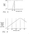
- the situation is depicted in the graph of FIG. 7 , showing the extinction coefficient of the amorphous carbon layer as a function of wavelength.
- the extinction coefficient is an indicator of the efficiency with which the amorphous carbon material absorbs radiation.
- FIG. 7 shows that the amorphous carbon layer extinction coefficient falls to a very low level above a wavelength of 1000 nm. Therefore, increasing the pyrometer wavelength above 950 is not a practical approach.
- the optical absorber (amorphous carbon) layer has an optical absorption coefficient that is at least at great as or greater than the optical absorption coefficient of the underlying substrate.
- the 40 nm window is too close to the laser emission band (centered around the laser wavelength) for a typical filter used to implement the pyrometer response band filter 63.
- the wavelength difference between the laser radiation peak at 810 nm and the beginning of the 40 nm window at 815 nm is extremely small. It is therefore difficult to block the laser radiation at 810 nm without also blocking the desired blackbody radiation (pyrometer signal) at 840 nm.
- This problem is solved by providing a razor-edge optical filter 72 in the system of FIGS. 2 and 5 , so that the conventional passband filter 63 is not required to block the laser radiation at 810 nm.
- the response of the conventional passband filter 63 may be such as to admit at least much of the laser radiation and thereby avoid inadvertently blocking or partially blocking the pyrometer wavelengths in the pyrometer response band.
- Blocking of the laser radiation is performed instead by the razor edge filter 72.
- the razor-edge optical filter 72 is a long wavelength pass filter, and has the optical response depicted in the graph of FIG. 8 .
- the cut-off wavelength of the razor edge filter 72 is at about 815 nm.
- the razor edge filter 72 has an edge transition from a transmittance of nearly 100% (full transmission or transparency) above the cut-off wavelength to only 10 -6 at (and below) the cut-off wavelength of 815 nm. This edge transition is extremely narrow, only five to eight nanometers wide.
- the razor edge filter blocks the laser radiation at 810 nm but is fully transparent to the pyrometer wavelength above 815 nm.
- Such an extremely sharp response is obtained by constructing the razor edge filter 72 as an interference filter.
- Interference filters are multilayer thin-film devices. They can be designed to function as an edge filter or bandpass filter. In either case, wavelength selection is based on the property of destructive light interference. In such a filter, incident light is passed through many pairs of coated reflecting surfaces. The distance between the reflective coatings determines which wavelengths destructively interfere and which wavelengths are in phase and will ultimately pass through the coatings. The gap between the reflecting surfaces is a thin film of dielectric material called a spacer. It has a thickness of one-half wave at the desired peak transmission wavelength.
- the reflecting layers can consist of several film layers, each of which is a quarter wavelength thick. This sandwich of quarterwave layers is made up of an alternating pattern of high and low index material, usually zinc sulfide and cryolite, respectively.
- the quarterwave coatings forming the reflective layer is called a stack.
- Such a razor-edge optical filter is available from Semrock, of Rochester, New York.
- the conventional bandpass filter 63 is selected to have a passband centered at about 840 nm, i.e., at about the center of the 40 nm window depicted in FIG. 6 .
- the 840 nm passband filter 63 has a full width half maximum of 10 nm, roughly corresponding to the response depicted in the graph of FIG. 9 . Being centered at 840 nm, it effectively blocks the fluorescence background emission from the optical components corresponding to the 950 nm peak in the graph of FIG. 6 .
- the pyrometer response band is established within the 40 nm window of FIG.
- the system of FIG. 5 further includes an optional notch filter 74 that blocks the laser emission at 810 nm.
- a processing system for thermally processing a workpiece includes: a source of laser radiation emitting at a laser wavelength; a beam splitting reflective surface, said source of laser radiation being positioned on a first side of said reflective surface; a substrate support for a substrate to be thermally processed; projection optics disposed between said first side of said reflective surface and said substrate support, at least one of said reflective surface and said projection optics comprising material having a fluorescence wavelength band lying above said laser wavelength; a pyrometer positioned on a second side of said reflective surface opposite first side, said pyrometer being sensitive to a pyrometer wavelength in a band lying between (a) the laser radiation wavelength and (b) the fluorescence wavelength band, wherein said projection optics images a region of said substrate being thermally processed onto said pyrometer; and a razor-edge filter having a cut-off wavelength edge transition, said filter tuned to block wavelengths lying below said edge transition and to pass wavelengths above said edge transition, said edge transition being less than 10 nm wide
- said substrate to be processed may be covered with an optical absorber layer comprising an amorphous carbon layer, said passband of said pyrometer filter lying in a wavelength range at which said amorphous carbon layer has an absorption coefficient at least as great as said substrate.
- said passband of said pyrometer filter may lie in a wavelength range at which said amorphous carbon layer has an absorption coefficient greater than that of said substrate.
- said edge transition may be between 5 and 8 nm wide, wherein said razor edge filter is about 100% transmissive at wavelengths above said cut-off wavelength and has an attenuation of about 10 -6 below said cut-off wavelength.
- said laser wavelength and said cut-off wavelength edge transition may be within separated by about 5 nm.
- said laser wavelength may be about 810 nm.
- Said fluorescence emission may be in a wavelength range from about 860 nm and peaking at about 950 nm.
- Said passband of said pyrometer filter may lie between about 820 nm and 860 nm.
- Said cut-off wavelength edge transition of said razor-edge filter may be near 815 nm.
- said pyrometer may include a photodetector and a notch filter passing said pyrometer wavelength and not passing said laser wavelength.
- said optics may project a line beam of radiation of said laser wavelength on said substrate.
- Said system may further comprise: line beam scanning apparatus having a fast axis transverse to said line beam.
- the system may further comprise a laser filter blocking wavelengths within the passband of said pyrometer passband filter, said laser filter being located in an optical path that includes said source of laser radiation and said projection optics, so as to block components of laser radiation within said passband from reaching said pyrometer.
- At least one of said reflective surface and said projection optics may be formed of a fused optical quartz material.
- a method of laser-annealing a substrate includes: emitting laser radiation emitting at a laser wavelength; passing said laser radiation in a forward direction through a beam splitter and projection optics to a substrate, at least one of the beam splitter and the projection optics comprising material having a fluorescence wavelength band lying above said laser wavelength; imaging the region of the substrate illuminated by the laser radiation onto a pyrometer through a pyrometer optical path, and admitting radiation through said pyrometer optical path lying in a pyrometer response band above the laser wavelength and below the fluorescence wavelength band; blocking radiation wavelengths in the pyrometer optical path below a cut-off wavelength edge transition and passing radiation wavelengths above said edge transition, said edge transition being less than 10 nm wide, said edge transition being above said laser wavelength and below said pyrometer wavelength; and blocking radiation wavelengths in the pyrometer optical path that lie within and above the fluorescence wavelength band, whereby to define a pyrometer response band lying above the laser wavelength and below the fluorescence wavelength
- the method may further comprise coating the substrate with an optical absorber layer comprising an amorphous carbon material prior to exposing the substrate to the laser radiation, said pyrometer response band lying in a wavelength range at which said amorphous carbon layer has an absorption coefficient at least as great as said substrate.
- said pyrometer response band may lie in a wavelength range at which said amorphous carbon layer has an absorption coefficient greater than that of said substrate.
- said edge transition may be between 5 and 8 nm wide, wherein said blocking the wavelengths below said edge transition comprises attenuating the wavelengths below said edge transition by a factor on the order of 10 -6 .
- said laser wavelength and said cut-off wavelength edge transition may be separated by about 5 nm.
Landscapes
- Physics & Mathematics (AREA)
- Optics & Photonics (AREA)
- Engineering & Computer Science (AREA)
- Plasma & Fusion (AREA)
- Mechanical Engineering (AREA)
- Recrystallisation Techniques (AREA)
- Laser Beam Processing (AREA)
Claims (15)
- Système de traitement pour le traitement thermique d'une pièce usinée, comprenant :une source de rayonnement laser (20, 32) émettant une longueur d'onde laser ;une surface réfléchissante de division de faisceau (54), ladite source de rayonnement laser étant positionnée sur un premier côté de ladite surface réfléchissante ;un support de substrat pour un substrat à traiter thermiquement ;des optiques de projection (62, 64, 66, 80, 82) disposées entre ledit premier côté de ladite surface réfléchissante et ledit support de substrat, lesdites optiques de projection étant conçues pour imager une région d'un substrat en cours de traitement thermique sur un pyromètre (60), l'un au moins parmi ladite surface réfléchissante et lesdites optiques de projection comprenant un matériau présentant une bande de longueur d'onde fluorescente plus élevée que ladite longueur d'onde laser ;le pyromètre, le pyromètre étant positionné sur un deuxième côté de ladite surface réfléchissante, opposé au premier côté, ledit pyromètre étant sensible à une longueur d'onde de pyromètre dans une bande comprise entre (a) la longueur d'onde de rayonnement laser et (b) la bande de longueur d'onde fluorescente ; etun filtre de bord tranchant (72) présentant une transition de bord de longueur d'onde de coupure, ledit filtre étant accordé pour bloquer des longueurs d'onde inférieures à ladite transition de bord et pour laisser passer des longueurs d'onde supérieures à ladite transition de bord, ladite transition de bord présentant une largeur inférieure à 10 nm, ladite transition de bord étant supérieure à ladite longueur d'onde laser et inférieure à ladite longueur d'onde de pyromètre ;un filtre de pyromètre (63) présentant une bande passante inférieure à ladite longueur d'onde de fluorescence.
- Système selon la revendication 1, dans lequel ledit substrat à traiter est recouvert d'une couche d'absorption optique comprenant une couche de carbone amorphe, ladite bande passante dudit filtre de pyromètre étant située dans une plage de longueur d'onde dans laquelle ladite couche de carbone amorphe présente un coefficient d'absorption au moins aussi élevé que celui dudit substrat.
- Système selon la revendication 2, dans lequel ladite bande passante dudit filtre de pyromètre se situe dans une plage de longueur d'onde dans laquelle ladite couche de carbone amorphe présente un coefficient d'absorption plus élevé que celui dudit substrat.
- Système selon la revendication 2, dans lequel ladite transition de bord présente une largeur comprise entre 5 nm et 8 nm, dans lequel ledit filtre de bord tranchant est transmissif à 100% environ à des longueurs d'onde supérieures à ladite longueur d'onde de coupure et présente une atténuation d'environ 10-6 en-dessous de ladite longueur d'onde de coupure.
- Système selon la revendication 4, dans lequel ladite longueur d'onde laser et ladite transition de bord de longueur d'onde de coupure sont séparées d'environ 5 nm.
- Système selon la revendication 4, dans lequel ladite longueur d'onde laser est d'environ 810 nm, ladite émission de fluorescence se situe dans une plage de longueur d'onde partant d'environ 860 nm et atteignant environ 950 nm, ladite bande passante dudit filtre de pyromètre étant comprise entre environ 820 nm et 860 nm, et ladite transition de bord de longueur d'onde de coupure dudit filtre de bord tranchant s'approchant de 815 nm.
- Système selon la revendication 1, dans lequel ledit pyromètre comprend un photodétecteur (61) et un filtre coupe-bande (67) laissant passer ladite longueur d'onde de pyromètre et bloquant ladite longueur d'onde laser.
- Système selon la revendication 1, dans lequel lesdites optiques projettent un faisceau linéaire (26) de rayonnement de ladite longueur d'onde laser sur ledit substrat, ledit système comprenant en outre :
un dispositif de balayage de faisceau linéaire (10) présentant un axe rapide transversal audit faisceau linéaire. - Système selon la revendication 1, comprenant en outre un filtre laser bloquant des longueurs d'onde comprise dans la bande passante dudit filtre passe-bande de pyromètre, ledit filtre laser se trouvant sur un chemin optique comprenant ladite source de rayonnement laser et lesdites optiques de projection, de manière à empêcher des composants de rayonnement laser compris dans ladite bande passante d'atteindre ledit pyromètre.
- Système selon la revendication 1, dans lequel l'un au moins parmi ladite surface réfléchissante et lesdites optiques de projection est constitué d'un matériau de quartz optique fusionné.
- Procédé pour le traitement thermique au laser d'un substrat (22), comprenant :l'émission d'un rayonnement laser à une longueur d'onde laser ;le passage dudit rayonnement laser dans une direction vers l'avant à travers un diviseur de faisceau (52, 54, 56) et des optiques de projection (62, 64, 66, 80, 82) vers un substrat (22), l'un au moins parmi le diviseur de faisceau et les optiques de projection comprenant un matériau présentent une bande de longueur d'onde de fluorescence plus élevée que ladite longueur d'onde laser ;l'imagerie de la région du substrat éclairée par le rayonnement laser sur un pyromètre (60) à travers un chemin optique de pyromètre, et l'admission d'un rayonnement à travers ledit chemin optique de pyromètre situé dans une bande de réponse de pyromètre supérieure à la longueur d'onde et inférieure à la bande de longueur d'onde de fluorescence ;le blocage des longueurs d'onde de rayonnement dans le chemin optique de pyromètre en dessous d'une transition de bord de longueur d'onde de coupure et le passage des longueurs d'onde de rayonnement au-dessus de ladite transition de bord de longueur d'onde, ladite transition de bord de longueur d'onde présentant une largeur inférieure à 10 nm, ladite transition de bord de longueur d'onde étant supérieure à ladite longueur d'onde laser et inférieure à ladite longueur d'onde de pyromètre ; etle blocage des longueurs d'onde de rayonnement dans le chemin optique de pyromètre situées dans la bande de longueur d'onde de fluorescence et au-dessus de celle-ci .
- Procédé selon la revendication 11, comprenant en outre le revêtement du substrat avec une couche d'absorption optique comprenant un matériau de carbone amorphe avant l'exposition du substrat au rayonnement laser, ladite bande de réponse de pyromètre étant située dans une plage de longueur d'onde dans laquelle ladite couche de carbone amorphe présente un coefficient d'absorption au moins aussi élevé que celui dudit substrat.
- Procédé selon la revendication 12, dans lequel ladite bande de réponse de pyromètre se situe dans une plage de longueur d'onde dans laquelle ladite couche de carbone amorphe présente un coefficient d'absorption plus élevé que celui dudit substrat.
- Procédé selon la revendication 12, dans lequel ladite transition de bord présente une largeur comprise entre 5 nm et 8 nm, dans lequel ledit blocage des longueurs d'onde inférieures à ladite transition de bord comprend l'atténuation des longueurs d'onde inférieures à ladite transition de bord selon un facteur de l'ordre de 10-6.
- Procédé selon la revendication 14, dans lequel ladite longueur d'onde laser et ladite transition de bord de longueur d'onde de coupure sont séparées d'environ 5 nm.
Applications Claiming Priority (3)
| Application Number | Priority Date | Filing Date | Title |
|---|---|---|---|
| US11/764,738 US7804042B2 (en) | 2007-06-18 | 2007-06-18 | Pryometer for laser annealing system compatible with amorphous carbon optical absorber layer |
| EP08767856.1A EP2167272B1 (fr) | 2007-06-18 | 2008-05-22 | Pyrometre pour systeme de recuit laser compatible avec une couche absorbante optique de carbone amorphe |
| PCT/US2008/006616 WO2008156543A1 (fr) | 2007-06-18 | 2008-05-22 | Pyromètre pour système de recuit laser compatible avec une couche absorbante optique de carbone amorphe |
Related Parent Applications (1)
| Application Number | Title | Priority Date | Filing Date |
|---|---|---|---|
| EP08767856.1A Division EP2167272B1 (fr) | 2007-06-18 | 2008-05-22 | Pyrometre pour systeme de recuit laser compatible avec une couche absorbante optique de carbone amorphe |
Publications (2)
| Publication Number | Publication Date |
|---|---|
| EP3330036A1 EP3330036A1 (fr) | 2018-06-06 |
| EP3330036B1 true EP3330036B1 (fr) | 2019-11-06 |
Family
ID=40131342
Family Applications (2)
| Application Number | Title | Priority Date | Filing Date |
|---|---|---|---|
| EP08767856.1A Active EP2167272B1 (fr) | 2007-06-18 | 2008-05-22 | Pyrometre pour systeme de recuit laser compatible avec une couche absorbante optique de carbone amorphe |
| EP18152336.6A Active EP3330036B1 (fr) | 2007-06-18 | 2008-05-22 | Pyromètre pour système de recuit au laser compatible avec une couche d'absorbeur optique de carbone amorphe |
Family Applications Before (1)
| Application Number | Title | Priority Date | Filing Date |
|---|---|---|---|
| EP08767856.1A Active EP2167272B1 (fr) | 2007-06-18 | 2008-05-22 | Pyrometre pour systeme de recuit laser compatible avec une couche absorbante optique de carbone amorphe |
Country Status (6)
| Country | Link |
|---|---|
| US (2) | US7804042B2 (fr) |
| EP (2) | EP2167272B1 (fr) |
| JP (1) | JP5431313B2 (fr) |
| KR (1) | KR101457345B1 (fr) |
| CN (1) | CN101678507B (fr) |
| WO (1) | WO2008156543A1 (fr) |
Families Citing this family (11)
| Publication number | Priority date | Publication date | Assignee | Title |
|---|---|---|---|---|
| US7947584B2 (en) * | 2008-05-02 | 2011-05-24 | Applied Materials, Inc. | Suitably short wavelength light for laser annealing of silicon in DSA type systems |
| US9429742B1 (en) * | 2011-01-04 | 2016-08-30 | Nlight, Inc. | High power laser imaging systems |
| US10095016B2 (en) | 2011-01-04 | 2018-10-09 | Nlight, Inc. | High power laser system |
| US9409255B1 (en) | 2011-01-04 | 2016-08-09 | Nlight, Inc. | High power laser imaging systems |
| US9720244B1 (en) | 2011-09-30 | 2017-08-01 | Nlight, Inc. | Intensity distribution management system and method in pixel imaging |
| CN103959442B (zh) | 2011-12-07 | 2017-09-15 | 应用材料公司 | 用于基板处理的激光反射仪 |
| CN103862169B (zh) * | 2012-12-12 | 2016-08-10 | 中芯国际集成电路制造(上海)有限公司 | 激光退火设备和方法 |
| US9310248B2 (en) | 2013-03-14 | 2016-04-12 | Nlight, Inc. | Active monitoring of multi-laser systems |
| CN105144355B (zh) | 2013-05-01 | 2018-02-06 | 应用材料公司 | 用于在晶片处理系统内进行低温测量的设备与方法 |
| US9709810B2 (en) | 2014-02-05 | 2017-07-18 | Nlight, Inc. | Single-emitter line beam system |
| US10247865B2 (en) * | 2017-07-24 | 2019-04-02 | Viavi Solutions Inc. | Optical filter |
Family Cites Families (19)
| Publication number | Priority date | Publication date | Assignee | Title |
|---|---|---|---|---|
| US6183130B1 (en) | 1998-02-20 | 2001-02-06 | Applied Materials, Inc. | Apparatus for substrate temperature measurement using a reflecting cavity and detector |
| US6535535B1 (en) * | 1999-02-12 | 2003-03-18 | Semiconductor Energy Laboratory Co., Ltd. | Laser irradiation method, laser irradiation apparatus, and semiconductor device |
| US6822787B1 (en) | 1999-04-26 | 2004-11-23 | Finisar Corporation | Lasing semiconductor optical amplifier with optical signal power monitor |
| US6531681B1 (en) * | 2000-03-27 | 2003-03-11 | Ultratech Stepper, Inc. | Apparatus having line source of radiant energy for exposing a substrate |
| JP3903761B2 (ja) * | 2001-10-10 | 2007-04-11 | 株式会社日立製作所 | レ−ザアニ−ル方法およびレ−ザアニ−ル装置 |
| KR20040063079A (ko) * | 2001-12-07 | 2004-07-12 | 소니 가부시끼 가이샤 | 광 조사 장치 및 레이저 어닐 장치 |
| KR100436218B1 (ko) * | 2001-12-24 | 2004-06-16 | 한국원자력연구소 | LiF에 Mg,Cu,Na, 및 Si를 첨가한 방사선계측용 열발광소자 및 그의 제조방법 |
| US8288239B2 (en) * | 2002-09-30 | 2012-10-16 | Applied Materials, Inc. | Thermal flux annealing influence of buried species |
| US6987240B2 (en) * | 2002-04-18 | 2006-01-17 | Applied Materials, Inc. | Thermal flux processing by scanning |
| JP4043859B2 (ja) * | 2002-06-18 | 2008-02-06 | 浜松ホトニクス株式会社 | 樹脂溶接装置及び樹脂溶接方法 |
| US6747245B2 (en) * | 2002-11-06 | 2004-06-08 | Ultratech Stepper, Inc. | Laser scanning apparatus and methods for thermal processing |
| US7109087B2 (en) * | 2003-10-03 | 2006-09-19 | Applied Materials, Inc. | Absorber layer for DSA processing |
| US7304310B1 (en) * | 2003-11-21 | 2007-12-04 | Kla-Tencor Technologies Corp. | Methods and systems for inspecting a specimen using light scattered in different wavelength ranges |
| US7078302B2 (en) * | 2004-02-23 | 2006-07-18 | Applied Materials, Inc. | Gate electrode dopant activation method for semiconductor manufacturing including a laser anneal |
| US7438468B2 (en) * | 2004-11-12 | 2008-10-21 | Applied Materials, Inc. | Multiple band pass filtering for pyrometry in laser based annealing systems |
| US7642205B2 (en) * | 2005-04-08 | 2010-01-05 | Mattson Technology, Inc. | Rapid thermal processing using energy transfer layers |
| US7279721B2 (en) * | 2005-04-13 | 2007-10-09 | Applied Materials, Inc. | Dual wavelength thermal flux laser anneal |
| US7312162B2 (en) * | 2005-05-17 | 2007-12-25 | Applied Materials, Inc. | Low temperature plasma deposition process for carbon layer deposition |
| US20060260545A1 (en) * | 2005-05-17 | 2006-11-23 | Kartik Ramaswamy | Low temperature absorption layer deposition and high speed optical annealing system |
-
2007
- 2007-06-18 US US11/764,738 patent/US7804042B2/en active Active
-
2008
- 2008-05-22 JP JP2010513186A patent/JP5431313B2/ja active Active
- 2008-05-22 EP EP08767856.1A patent/EP2167272B1/fr active Active
- 2008-05-22 CN CN200880020796XA patent/CN101678507B/zh active Active
- 2008-05-22 WO PCT/US2008/006616 patent/WO2008156543A1/fr active Application Filing
- 2008-05-22 EP EP18152336.6A patent/EP3330036B1/fr active Active
- 2008-05-22 KR KR1020107001143A patent/KR101457345B1/ko active IP Right Grant
-
2010
- 2010-09-21 US US12/886,809 patent/US8232503B2/en active Active
Non-Patent Citations (1)
| Title |
|---|
| None * |
Also Published As
| Publication number | Publication date |
|---|---|
| JP2010530639A (ja) | 2010-09-09 |
| US8232503B2 (en) | 2012-07-31 |
| WO2008156543A1 (fr) | 2008-12-24 |
| KR101457345B1 (ko) | 2014-11-04 |
| US7804042B2 (en) | 2010-09-28 |
| EP2167272A1 (fr) | 2010-03-31 |
| CN101678507A (zh) | 2010-03-24 |
| EP2167272B1 (fr) | 2018-01-24 |
| US20080308534A1 (en) | 2008-12-18 |
| US20110006044A1 (en) | 2011-01-13 |
| EP2167272A4 (fr) | 2016-11-23 |
| CN101678507B (zh) | 2012-11-28 |
| EP3330036A1 (fr) | 2018-06-06 |
| KR20100044786A (ko) | 2010-04-30 |
| JP5431313B2 (ja) | 2014-03-05 |
Similar Documents
| Publication | Publication Date | Title |
|---|---|---|
| EP3330036B1 (fr) | Pyromètre pour système de recuit au laser compatible avec une couche d'absorbeur optique de carbone amorphe | |
| EP1831658B1 (fr) | Filtrage passe-bande multiple pour pyrometrie dans des systemes de recuit a base de laser | |
| US7422988B2 (en) | Rapid detection of imminent failure in laser thermal processing of a substrate | |
| US7494272B2 (en) | Dynamic surface annealing using addressable laser array with pyrometry feedback | |
| US7910499B2 (en) | Autofocus for high power laser diode based annealing system | |
| US8674257B2 (en) | Automatic focus and emissivity measurements for a substrate system | |
| US7129440B2 (en) | Single axis light pipe for homogenizing slow axis of illumination systems based on laser diodes | |
| JP4777995B2 (ja) | 集光ビームを測定する為の方法および装置 |
Legal Events
| Date | Code | Title | Description |
|---|---|---|---|
| PUAI | Public reference made under article 153(3) epc to a published international application that has entered the european phase |
Free format text: ORIGINAL CODE: 0009012 |
|
| STAA | Information on the status of an ep patent application or granted ep patent |
Free format text: STATUS: THE APPLICATION HAS BEEN PUBLISHED |
|
| AC | Divisional application: reference to earlier application |
Ref document number: 2167272 Country of ref document: EP Kind code of ref document: P |
|
| AK | Designated contracting states |
Kind code of ref document: A1 Designated state(s): AT BE BG CH CY CZ DE DK EE ES FI FR GB GR HR HU IE IS IT LI LT LU LV MC MT NL NO PL PT RO SE SI SK TR |
|
| STAA | Information on the status of an ep patent application or granted ep patent |
Free format text: STATUS: REQUEST FOR EXAMINATION WAS MADE |
|
| 17P | Request for examination filed |
Effective date: 20180928 |
|
| RBV | Designated contracting states (corrected) |
Designated state(s): AT BE BG CH CY CZ DE DK EE ES FI FR GB GR HR HU IE IS IT LI LT LU LV MC MT NL NO PL PT RO SE SI SK TR |
|
| RIC1 | Information provided on ipc code assigned before grant |
Ipc: B23K 26/04 20140101AFI20190408BHEP |
|
| GRAP | Despatch of communication of intention to grant a patent |
Free format text: ORIGINAL CODE: EPIDOSNIGR1 |
|
| STAA | Information on the status of an ep patent application or granted ep patent |
Free format text: STATUS: GRANT OF PATENT IS INTENDED |
|
| INTG | Intention to grant announced |
Effective date: 20190528 |
|
| GRAS | Grant fee paid |
Free format text: ORIGINAL CODE: EPIDOSNIGR3 |
|
| GRAA | (expected) grant |
Free format text: ORIGINAL CODE: 0009210 |
|
| STAA | Information on the status of an ep patent application or granted ep patent |
Free format text: STATUS: THE PATENT HAS BEEN GRANTED |
|
| AC | Divisional application: reference to earlier application |
Ref document number: 2167272 Country of ref document: EP Kind code of ref document: P |
|
| AK | Designated contracting states |
Kind code of ref document: B1 Designated state(s): AT BE BG CH CY CZ DE DK EE ES FI FR GB GR HR HU IE IS IT LI LT LU LV MC MT NL NO PL PT RO SE SI SK TR |
|
| REG | Reference to a national code |
Ref country code: GB Ref legal event code: FG4D |
|
| REG | Reference to a national code |
Ref country code: CH Ref legal event code: EP Ref country code: AT Ref legal event code: REF Ref document number: 1198099 Country of ref document: AT Kind code of ref document: T Effective date: 20191115 |
|
| REG | Reference to a national code |
Ref country code: IE Ref legal event code: FG4D |
|
| REG | Reference to a national code |
Ref country code: DE Ref legal event code: R096 Ref document number: 602008061613 Country of ref document: DE |
|
| REG | Reference to a national code |
Ref country code: NL Ref legal event code: MP Effective date: 20191106 |
|
| REG | Reference to a national code |
Ref country code: LT Ref legal event code: MG4D |
|
| PG25 | Lapsed in a contracting state [announced via postgrant information from national office to epo] |
Ref country code: LT Free format text: LAPSE BECAUSE OF FAILURE TO SUBMIT A TRANSLATION OF THE DESCRIPTION OR TO PAY THE FEE WITHIN THE PRESCRIBED TIME-LIMIT Effective date: 20191106 Ref country code: GR Free format text: LAPSE BECAUSE OF FAILURE TO SUBMIT A TRANSLATION OF THE DESCRIPTION OR TO PAY THE FEE WITHIN THE PRESCRIBED TIME-LIMIT Effective date: 20200207 Ref country code: PL Free format text: LAPSE BECAUSE OF FAILURE TO SUBMIT A TRANSLATION OF THE DESCRIPTION OR TO PAY THE FEE WITHIN THE PRESCRIBED TIME-LIMIT Effective date: 20191106 Ref country code: BG Free format text: LAPSE BECAUSE OF FAILURE TO SUBMIT A TRANSLATION OF THE DESCRIPTION OR TO PAY THE FEE WITHIN THE PRESCRIBED TIME-LIMIT Effective date: 20200206 Ref country code: FI Free format text: LAPSE BECAUSE OF FAILURE TO SUBMIT A TRANSLATION OF THE DESCRIPTION OR TO PAY THE FEE WITHIN THE PRESCRIBED TIME-LIMIT Effective date: 20191106 Ref country code: NL Free format text: LAPSE BECAUSE OF FAILURE TO SUBMIT A TRANSLATION OF THE DESCRIPTION OR TO PAY THE FEE WITHIN THE PRESCRIBED TIME-LIMIT Effective date: 20191106 Ref country code: LV Free format text: LAPSE BECAUSE OF FAILURE TO SUBMIT A TRANSLATION OF THE DESCRIPTION OR TO PAY THE FEE WITHIN THE PRESCRIBED TIME-LIMIT Effective date: 20191106 Ref country code: SE Free format text: LAPSE BECAUSE OF FAILURE TO SUBMIT A TRANSLATION OF THE DESCRIPTION OR TO PAY THE FEE WITHIN THE PRESCRIBED TIME-LIMIT Effective date: 20191106 Ref country code: NO Free format text: LAPSE BECAUSE OF FAILURE TO SUBMIT A TRANSLATION OF THE DESCRIPTION OR TO PAY THE FEE WITHIN THE PRESCRIBED TIME-LIMIT Effective date: 20200206 Ref country code: PT Free format text: LAPSE BECAUSE OF FAILURE TO SUBMIT A TRANSLATION OF THE DESCRIPTION OR TO PAY THE FEE WITHIN THE PRESCRIBED TIME-LIMIT Effective date: 20200306 |
|
| PG25 | Lapsed in a contracting state [announced via postgrant information from national office to epo] |
Ref country code: IS Free format text: LAPSE BECAUSE OF FAILURE TO SUBMIT A TRANSLATION OF THE DESCRIPTION OR TO PAY THE FEE WITHIN THE PRESCRIBED TIME-LIMIT Effective date: 20200306 Ref country code: HR Free format text: LAPSE BECAUSE OF FAILURE TO SUBMIT A TRANSLATION OF THE DESCRIPTION OR TO PAY THE FEE WITHIN THE PRESCRIBED TIME-LIMIT Effective date: 20191106 |
|
| PG25 | Lapsed in a contracting state [announced via postgrant information from national office to epo] |
Ref country code: ES Free format text: LAPSE BECAUSE OF FAILURE TO SUBMIT A TRANSLATION OF THE DESCRIPTION OR TO PAY THE FEE WITHIN THE PRESCRIBED TIME-LIMIT Effective date: 20191106 Ref country code: CZ Free format text: LAPSE BECAUSE OF FAILURE TO SUBMIT A TRANSLATION OF THE DESCRIPTION OR TO PAY THE FEE WITHIN THE PRESCRIBED TIME-LIMIT Effective date: 20191106 Ref country code: RO Free format text: LAPSE BECAUSE OF FAILURE TO SUBMIT A TRANSLATION OF THE DESCRIPTION OR TO PAY THE FEE WITHIN THE PRESCRIBED TIME-LIMIT Effective date: 20191106 Ref country code: DK Free format text: LAPSE BECAUSE OF FAILURE TO SUBMIT A TRANSLATION OF THE DESCRIPTION OR TO PAY THE FEE WITHIN THE PRESCRIBED TIME-LIMIT Effective date: 20191106 Ref country code: EE Free format text: LAPSE BECAUSE OF FAILURE TO SUBMIT A TRANSLATION OF THE DESCRIPTION OR TO PAY THE FEE WITHIN THE PRESCRIBED TIME-LIMIT Effective date: 20191106 |
|
| REG | Reference to a national code |
Ref country code: DE Ref legal event code: R097 Ref document number: 602008061613 Country of ref document: DE |
|
| REG | Reference to a national code |
Ref country code: AT Ref legal event code: MK05 Ref document number: 1198099 Country of ref document: AT Kind code of ref document: T Effective date: 20191106 |
|
| PG25 | Lapsed in a contracting state [announced via postgrant information from national office to epo] |
Ref country code: SK Free format text: LAPSE BECAUSE OF FAILURE TO SUBMIT A TRANSLATION OF THE DESCRIPTION OR TO PAY THE FEE WITHIN THE PRESCRIBED TIME-LIMIT Effective date: 20191106 |
|
| PLBE | No opposition filed within time limit |
Free format text: ORIGINAL CODE: 0009261 |
|
| STAA | Information on the status of an ep patent application or granted ep patent |
Free format text: STATUS: NO OPPOSITION FILED WITHIN TIME LIMIT |
|
| 26N | No opposition filed |
Effective date: 20200807 |
|
| PG25 | Lapsed in a contracting state [announced via postgrant information from national office to epo] |
Ref country code: AT Free format text: LAPSE BECAUSE OF FAILURE TO SUBMIT A TRANSLATION OF THE DESCRIPTION OR TO PAY THE FEE WITHIN THE PRESCRIBED TIME-LIMIT Effective date: 20191106 Ref country code: SI Free format text: LAPSE BECAUSE OF FAILURE TO SUBMIT A TRANSLATION OF THE DESCRIPTION OR TO PAY THE FEE WITHIN THE PRESCRIBED TIME-LIMIT Effective date: 20191106 |
|
| PG25 | Lapsed in a contracting state [announced via postgrant information from national office to epo] |
Ref country code: MC Free format text: LAPSE BECAUSE OF FAILURE TO SUBMIT A TRANSLATION OF THE DESCRIPTION OR TO PAY THE FEE WITHIN THE PRESCRIBED TIME-LIMIT Effective date: 20191106 Ref country code: IT Free format text: LAPSE BECAUSE OF FAILURE TO SUBMIT A TRANSLATION OF THE DESCRIPTION OR TO PAY THE FEE WITHIN THE PRESCRIBED TIME-LIMIT Effective date: 20191106 Ref country code: CH Free format text: LAPSE BECAUSE OF NON-PAYMENT OF DUE FEES Effective date: 20200531 Ref country code: LI Free format text: LAPSE BECAUSE OF NON-PAYMENT OF DUE FEES Effective date: 20200531 |
|
| REG | Reference to a national code |
Ref country code: BE Ref legal event code: MM Effective date: 20200531 |
|
| GBPC | Gb: european patent ceased through non-payment of renewal fee |
Effective date: 20200522 |
|
| PG25 | Lapsed in a contracting state [announced via postgrant information from national office to epo] |
Ref country code: LU Free format text: LAPSE BECAUSE OF NON-PAYMENT OF DUE FEES Effective date: 20200522 |
|
| PG25 | Lapsed in a contracting state [announced via postgrant information from national office to epo] |
Ref country code: IE Free format text: LAPSE BECAUSE OF NON-PAYMENT OF DUE FEES Effective date: 20200522 Ref country code: GB Free format text: LAPSE BECAUSE OF NON-PAYMENT OF DUE FEES Effective date: 20200522 |
|
| PG25 | Lapsed in a contracting state [announced via postgrant information from national office to epo] |
Ref country code: BE Free format text: LAPSE BECAUSE OF NON-PAYMENT OF DUE FEES Effective date: 20200531 |
|
| PG25 | Lapsed in a contracting state [announced via postgrant information from national office to epo] |
Ref country code: TR Free format text: LAPSE BECAUSE OF FAILURE TO SUBMIT A TRANSLATION OF THE DESCRIPTION OR TO PAY THE FEE WITHIN THE PRESCRIBED TIME-LIMIT Effective date: 20191106 Ref country code: MT Free format text: LAPSE BECAUSE OF FAILURE TO SUBMIT A TRANSLATION OF THE DESCRIPTION OR TO PAY THE FEE WITHIN THE PRESCRIBED TIME-LIMIT Effective date: 20191106 Ref country code: CY Free format text: LAPSE BECAUSE OF FAILURE TO SUBMIT A TRANSLATION OF THE DESCRIPTION OR TO PAY THE FEE WITHIN THE PRESCRIBED TIME-LIMIT Effective date: 20191106 |
|
| PGFP | Annual fee paid to national office [announced via postgrant information from national office to epo] |
Ref country code: DE Payment date: 20220420 Year of fee payment: 15 |
|
| REG | Reference to a national code |
Ref country code: DE Ref legal event code: R119 Ref document number: 602008061613 Country of ref document: DE |
|
| PG25 | Lapsed in a contracting state [announced via postgrant information from national office to epo] |
Ref country code: DE Free format text: LAPSE BECAUSE OF NON-PAYMENT OF DUE FEES Effective date: 20231201 |
|
| PGFP | Annual fee paid to national office [announced via postgrant information from national office to epo] |
Ref country code: FR Payment date: 20240418 Year of fee payment: 17 |