EP3328558B1 - Extended range ultrasound transducer - Google Patents
Extended range ultrasound transducer Download PDFInfo
- Publication number
- EP3328558B1 EP3328558B1 EP16833696.4A EP16833696A EP3328558B1 EP 3328558 B1 EP3328558 B1 EP 3328558B1 EP 16833696 A EP16833696 A EP 16833696A EP 3328558 B1 EP3328558 B1 EP 3328558B1
- Authority
- EP
- European Patent Office
- Prior art keywords
- ultrasonic
- transmitter
- interposer
- transducer
- array
- Prior art date
- Legal status (The legal status is an assumption and is not a legal conclusion. Google has not performed a legal analysis and makes no representation as to the accuracy of the status listed.)
- Active
Links
Images

Classifications
-
- B—PERFORMING OPERATIONS; TRANSPORTING
- B06—GENERATING OR TRANSMITTING MECHANICAL VIBRATIONS IN GENERAL
- B06B—METHODS OR APPARATUS FOR GENERATING OR TRANSMITTING MECHANICAL VIBRATIONS OF INFRASONIC, SONIC, OR ULTRASONIC FREQUENCY, e.g. FOR PERFORMING MECHANICAL WORK IN GENERAL
- B06B1/00—Methods or apparatus for generating mechanical vibrations of infrasonic, sonic, or ultrasonic frequency
- B06B1/02—Methods or apparatus for generating mechanical vibrations of infrasonic, sonic, or ultrasonic frequency making use of electrical energy
- B06B1/06—Methods or apparatus for generating mechanical vibrations of infrasonic, sonic, or ultrasonic frequency making use of electrical energy operating with piezoelectric effect or with electrostriction
- B06B1/0607—Methods or apparatus for generating mechanical vibrations of infrasonic, sonic, or ultrasonic frequency making use of electrical energy operating with piezoelectric effect or with electrostriction using multiple elements
- B06B1/0622—Methods or apparatus for generating mechanical vibrations of infrasonic, sonic, or ultrasonic frequency making use of electrical energy operating with piezoelectric effect or with electrostriction using multiple elements on one surface
- B06B1/0629—Square array
-
- B—PERFORMING OPERATIONS; TRANSPORTING
- B06—GENERATING OR TRANSMITTING MECHANICAL VIBRATIONS IN GENERAL
- B06B—METHODS OR APPARATUS FOR GENERATING OR TRANSMITTING MECHANICAL VIBRATIONS OF INFRASONIC, SONIC, OR ULTRASONIC FREQUENCY, e.g. FOR PERFORMING MECHANICAL WORK IN GENERAL
- B06B1/00—Methods or apparatus for generating mechanical vibrations of infrasonic, sonic, or ultrasonic frequency
- B06B1/02—Methods or apparatus for generating mechanical vibrations of infrasonic, sonic, or ultrasonic frequency making use of electrical energy
- B06B1/0292—Electrostatic transducers, e.g. electret-type
-
- B—PERFORMING OPERATIONS; TRANSPORTING
- B06—GENERATING OR TRANSMITTING MECHANICAL VIBRATIONS IN GENERAL
- B06B—METHODS OR APPARATUS FOR GENERATING OR TRANSMITTING MECHANICAL VIBRATIONS OF INFRASONIC, SONIC, OR ULTRASONIC FREQUENCY, e.g. FOR PERFORMING MECHANICAL WORK IN GENERAL
- B06B1/00—Methods or apparatus for generating mechanical vibrations of infrasonic, sonic, or ultrasonic frequency
- B06B1/02—Methods or apparatus for generating mechanical vibrations of infrasonic, sonic, or ultrasonic frequency making use of electrical energy
- B06B1/06—Methods or apparatus for generating mechanical vibrations of infrasonic, sonic, or ultrasonic frequency making use of electrical energy operating with piezoelectric effect or with electrostriction
- B06B1/0607—Methods or apparatus for generating mechanical vibrations of infrasonic, sonic, or ultrasonic frequency making use of electrical energy operating with piezoelectric effect or with electrostriction using multiple elements
- B06B1/0622—Methods or apparatus for generating mechanical vibrations of infrasonic, sonic, or ultrasonic frequency making use of electrical energy operating with piezoelectric effect or with electrostriction using multiple elements on one surface
Definitions
- the invention relates generally to ultrasound transducers, and to combined discrete transmitter circuitry with a separate ultrasonic transducer receiver array.
- Ultrasound transducers exist for transmitting ultrasound waves and detecting a reflection or echo of the transmitted wave. Such devices are also sometimes referred to as ultrasound or ultrasonic transducers or transceivers. Ultrasound transducers have myriad uses, including consumer devices, vehicle safety, and medical diagnostics. In these and other fields, signals detected by the transducer may be processed to determine distance which may be further combined with directional or area processing to determine shape and aspects in connection with two and three dimensional processing, including image processing.
- a micromachined ultrasonic transducer (MUT) array is commonly used in conventional implementations as an ultrasound transducer to perform both the transmission of ultrasonic sounds and the detection of the sound echo.
- Such an array is typically formed using semiconductor processing, whereby an array of micromachined mechanical elements is created relative to the semiconductor substrate. Each array element has a same construction but is separately excitable to transmit a signal and separately readable to detect the signal echo.
- the pMUT array elements function in response to the known nature of piezoelectric materials combined sometimes with a thin film membrane, which collectively generate electricity from applied mechanical strain and, in a reversible process, generate a mechanical strain from applied electricity.
- the cMUT array elements function in response to the known nature of capacitive structure and in combination with an associated membrane, so the elements generate an alternating electrical signal from a change in capacitance caused by vibration of the membrane and, in a reversible process, generate vibration of the membrane from an applied alternating signal across the capacitor.
- acoustic power is a function of the product of pressure, area, and velocity
- the membrane used in a MUT may limit the transmission power because of limitations in sustaining pressure, a relatively small areal coverage on part of the transducer surface, and also due to reduced velocity form non-uniformities across the membrane.
- the number of elements in the MUT array are often increased to achieve greater resolution or other performance, and wire bonding or flex cable are often implemented for interconnectivity to each element, so a large number of elements (e.g., 50x50 or above) creates considerable complexity and cost in a wire bundle or cable to electrically communicate with all elements.
- US 2013/315035 and US 2013/257224 disclose both an ultrasonic transducer, comprising: an interposer having electrical connectivity contacts;an ultrasonic receiver, including an array of receiving elements, physically fixed relative to the interposer and coupled to electrically communicate with electrical connectivity contacts of the interposer; and at least one ultrasonic transmitter, separate from the ultrasonic receiver, physically fixed relative to the interposer and coupled to electrically communicate with electrical connectivity contacts of the interposer; wherein the ultrasonic receiver is physically fixed adjacent a first side of the interposer.
- US 2013/261467 relates to ultrasonic transducers and to a method of forming a connection with a laterally-facing piezoelectric micromachined ultrasonic transducer housed in a catheter.
- US 2013/214641 relates to an ultrasound transducer includes an array of acoustic elements, an integrated circuit, and an interposer.
- the interposer includes conductive elements that electrically connect the array of acoustic elements to the integrated circuit.
- An electrically conductive adhesive is engaged with the conductive elements of the interposer to electrically connect the interposer to at least one of the integrated circuit or the array of acoustic elements.
- an ultrasonic transducer has an interposer having electrical connectivity contacts.
- the ultrasonic transducer also has an ultrasonic receiver, including an array of receiving elements, physically fixed relative to the interposer and coupled to electrically communicate with electrical connectivity contacts of the interposer.
- the ultrasonic transducer also has at least one ultrasonic transmitter, separate from the ultrasonic receiver, physically fixed relative to the interposer and coupled to electrically communicate with electrical connectivity contacts of the interposer.
- FIG. 1 illustrates an electrical block diagram of an ultrasound transducer 10 per the preferred embodiments.
- Various matters known in the transducer field may be used to supplement the block and functional description of this document.
- the preferred embodiments, therefore, are described with this understanding and with a concentration on the combination of certain technologies and layouts to achieve an overall ultrasound transducer device that provides advantages over conventional implementations.
- Ultrasound transducer 10 is constructed to include an interposer (or carrier) 12 that provides a structural and electrical foundation for connection to various other devices that are part of the overall device.
- interposer 12 may be a printed or other type of circuit board.
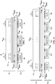
- FIG. 1 illustrates a first side S 1 of interposer 12
- FIG. 3 illustrates a second side S 2 , which is the opposite of side S 1 , of interposer 12
- FIG. 5 illustrates a partial cross-sectional view across interposer 12.
- an ultrasound receiver array 14 which may be constructed as various types of micromachined ultrasonic transducer receiver (MUT) arrays, known and further being developed.
- MUT arrays are commonly used both to transmit ultrasound waves and then detect their resultant echo; however, in the preferred embodiments, while using this same structure, array 14 is functionally used as an ultrasound receiver (i.e., imager), whereas as discussed below different apparatus is used as an ultrasound transmitter.
- Array 14 as shown as being two-dimensional, having rows and columns of elements. For the illustrated embodiment, various elements are labeled with a coordinate shown as EL(row number, column number).
- each element EL( x , y ) provides a cavity, shown generally in FIG. 1 as a small square, where the cavity is surrounded by a material from which all the elements are formed; thus, array 14 may be formed by starting with a silicon member (e.g., square or circular) and forming the elements therein. Further, each element usually has a membrane along the bottom of the element cavity that will flex in response to response to receiving an ultrasound wave.
- the total number of row and column elements EL( x , y ) are the same and equal to x+1, where preferably x is at least 7, and more preferably x is 49 or greater.
- the number of row elements could differ from the number of column elements.
- array 14 could be linear, whereby its elements are aligned in a single line. And in still another alternative embodiment, array 14 could be annular. Array 14 also may be constructed using various MUT technologies.
- One example embodiment uses a piezoelectric micromachined ultrasonic transducer (pMUT) as array 14.
- An alternatively preferred embodiment uses a capacitive micromachined ultrasonic transducer (cMUT), although a tradeoff is expected to include a higher cost of manufacturing.
- pMUT or cMUT may be constructed relative to a (e.g., silicon) wafer using known and developed semiconductor and micromachining fabrication technologies, so that the elements are formed in part from the wafer material, as further described below.
- array elements are formed in connection with a semiconductor wafer, with a partial illustration shown in FIG. 2 .
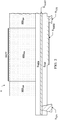
- FIG. 2 illustrates an example, in cross-sectional view, of an element EL that may represent any of the various elements in of array 14 in FIG. 1 .
- Element EL includes a semiconductor surrounding a cavity in three-dimensional space, so the cross-sectional view of FIG. 2 illustrates this as two semiconductor sidewall members MEM SW along with a rear wall member MEM RW shown by and below a dashed line; in the illustrated cross-section, the front wall that otherwise would complete the surround around the element is not visible, but is further included, as also visible in FIG. 1 .
- all such members MEM may be formed or result, such as by directionally etching from a surface of a semiconductor substrate or wafer, thereby creating respective cavities enclosed by surrounding semiconductor material, referred to herein as sidewall, front wall, and rear wall members for sake of reference.
- the members MEM are therefore the height of the original semiconductor substrate, with a usual contemporary example being 400 microns. Further therefore, with such a structure, preferably the cavities of each element are generally of the same size and shape. The design of cavity dimensions for acoustic performance is known.
- An element membrane EL MEM is a layer adjacent one end of all the members and contiguous over the cavity.
- element membrane EL MEM is in the range of 2 to 10 microns thick and extends across numerous different elements ( e.g ., across the entire array). Therefore, the drawings are not to scale, as the element membrane EL MEM is virtually indiscernible to view, as compared to the 400 microns or so of the members MEM.
- membrane EL MEM is formed as an insulator (e.g ., silicon dioxide or silicon nitride), as such materials are common in semiconductor manufacturing.
- insulator e.g ., silicon dioxide or silicon nitride
- Another preferable attribute of element membrane EL MEM is being inert to chemicals, where such insulators are inert to a variety of common chemicals.
- Membrane EL MEM is a mechanical structural element that sustains pressure from fluids (e.g., air) that transmit acoustic signals, so for each element, the pressure sustained in the cavity is received by the portion of membrane EL MEM under the cavity.
- fluids e.g., air
- Adjacent to element membrane EL MEM is a conductive layer providing a first electrode EL ELEC1 , which is preferably a metal layer in the range of 0.1 to 1 micron thick.
- First electrode EL ELEC1 also is not illustrated to scale, relative to the members MEM.
- Electrode EL ELEC1 also preferably extends across numerous different elements ( e.g ., across the entire array). Alternatively, each element can have a separate electrode EL ELEC1 that is electrically isolated from other elements.
- first electrode EL ELEC1 Adjacent to first electrode EL ELEC1 is a piezoelectric film layer EL PZF , which as its name suggest is a piezoelectric layer, and it is the range of 0.1 to 2 microns thick (also not shown to scale relative to members MEM). Piezoelectric film layer EL PZF also preferably extends across numerous different elements ( e.g ., across the entire array), but its flexure under the cavity of an individual element is represented by electrical signals to detect a measure of ultrasound wave receipt by that element. Alternatively, each element can have a disjoint piezoelectric film layer EL PZF so to further isolate electrical signals generated between different elements.
- Adjacent piezoelectric film layer EL PZF is a conductive layer providing a second electrode EL ELEC2 , which is preferably a metal layer in the range of 0.1 to 1 micron thick (also not shown to scale relative to members MEM). Second electrode EL ELEC2 does not apply across multiple elements, but instead is sized to be less than the cavity for a given cell except for a portion of that electrode that extends beyond the width of the cavity to provide an interconnect, as further detailed below. For example, therefore, electrode EL ELEC2 may have dimensions in the range of 10% to 80% of the cavity area.
- a first conductive contact EL CT1 may be a metal formed through an opening created in piezoelectric film layer EL PZF , to reach a portion of first electrode EL ELEC1 , and a second and separate conductive contact EL CT2 is connected to EL ELEC2 .
- first conductive contact EL CT1 is provided to electrically communicate first electrode EL ELEC1
- a second conductive contact EL CT2 is provided to electrically communicate second electrode EL ELEC2 , as interconnects to an interposer, as detailed below. Electrodes EL ELEC1 and EL ELEC2 are capacitively coupled.
- each element of array 14 is operable to receive an ultrasonic reflection and, due to its structure and materials, provide an electrical signal representative of the received reflection.
- the first electrode EL ELEC1 may be connected to a reference potential such as ground, and the voltage on second electrode EL ELEC2 of any element may be electrically sensed relative to the reference, with that difference representing the flexure of piezoelectric film layer EL PZF , in response to receiving an ultrasonic wave.
- additional circuitry described below, is connected to separately access each such element so that any combination of respective elements signals may be processed to further develop information from the received reflections.
- FIG. 3 illustrates side S 2 of interposer 12.
- physically attached to side S 2 are three separate electrical and operational blocks, including a receive (RX) analog-front-end (AFE) 16, an ultrasonic transmitter 18, and a transmit (TX) driver 20.
- RX receive
- AFE analog-front-end
- TX transmit
- RX AFE 16 is preferably an integrated circuit and includes analog signal conditioning circuitry, such as operational amplifiers and filters that provide a configurable electronic functional block for interfacing the analog signals provided by elements in ultrasound receiver array 14 to an external (e.g ., digital) circuit, such as an outside processor (e.g ., microcontroller, digital signal processor, microprocessor).
- analog signal conditioning circuitry such as operational amplifiers and filters that provide a configurable electronic functional block for interfacing the analog signals provided by elements in ultrasound receiver array 14 to an external (e.g ., digital) circuit, such as an outside processor (e.g ., microcontroller, digital signal processor, microprocessor).
- an outside processor e.g ., microcontroller, digital signal processor, microprocessor
- Transmitter 18 includes the actuator for generating the ultrasonic sound waves, independent of, and apart from, receiver array 14.
- a MUT (such as may be implemented in receiver array 14) is used in some conventional implementations as a transmitter; however, in the preferred embodiments, the ultrasonic transmission functionality is provided by independent apparatus.
- transmitter 18 may be constructed from various technologies, known or ascertainable.
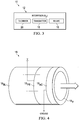
- transmitter 18 is shown in a perspective view in FIG. 4 .
- transmitter 18 is a single element ultrasonic transmitter, preferably constructed using bulk piezoelectric ceramic; in this regard, FIG.
- FIG. 4 illustrates a transmitter with a generally circular cross-section and having a single plate piezoelectric element 18 PE made of piezoelectric ceramic, such as lead zirconate titanate (PZT) or single crystal lead magnesium niobate-lead titanate solid solution (PMN-PT), sandwiched by two electrodes to couple to electrical excitations.
- PZT lead zirconate titanate
- PMN-PT single crystal lead magnesium niobate-lead titanate solid solution
- the preferred embodiment implements bulk ceramics for transmitting ultrasound waves, which thereby afford much greater power as compared to certain other types of transmitters, such as if a MUT were used for the transmitter.
- a thicker bulk ceramic can sustain greater voltage and allow more electric power converted through strain energy, as compared to MUT technology.
- TX driver 20 is included in the preferred embodiment inasmuch as the power and noise requirements are likely to differ as between the lower power needs of RX AFE 16 and the higher power needs of transmitter 18.
- TX driver 20 is preferably an integrated circuit and includes circuitry that provides level shifting as between the lower power available for RX AFE 16 and the higher power needed for transmitter 18. Such level shifting may include control/regulation of current and voltage within a varying range of input voltages.
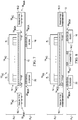
- FIG. 5 illustrates a cross-sectional view across interposer 12 and other items described above, where additional details are now observed.
- each of array 14, RX AFE 16, transmitter 18, and TX driver 20 is physical and electrically interconnected to interposer 12.
- each of these items is constructed using bumping metallization or other flip chip bumps such as solder or plated copper so that contacts, such as via miniature ball grid arrays (BGA), may be used to both physically and electrically connect each respective circuit to conductors on interposer 12.
- array 14 is shown to have a respective BGA 14 BGA to connect to side S 1 of interposer 12 to electrodes of array 14, where as shown in FIG.
- each of RX AFE 16, transmitter 18, and TX driver 20 has a respective BGA 16 BGA , 18 BGAE , and 20 BGA to connect to side S 2 of interposer 12.
- the relatively large number of elements of array 14 will give rise to a shorter pitch and greater connectivity density among BGA 14 BGA , as compared to that of arrays BGA 16 BGA , 18 BGA , and 20 BGA .
- the former may be in the range of usually less than 250 microns, or less than 100 microns, or even less than 50 micron, while the latter is in the range of usually greater than 400 microns.
- the BGA (or other connectors) between transmitter 18 and interposer 12 are positioned to be out of the path of the acoustic wave transmitted by transmitter 18, which in the orientation of FIG. 5 is upward.
- Transmitter 18 also may be electrically connected to interposer 12 with other package footprints, such as used in quad flat packages (QFP), quad flat no-leads packages (QFN), or other outline packages such small outline integrated circuit (SOIC), or through-hole connectors.
- QFP quad flat packages
- QFN quad flat no-leads packages
- SOIC small outline integrated circuit
- FIG. 5 also illustrates that an acoustic couplant layer (or multiple layers) 14 AC1 is formed upward between and vertically beyond the substrate members ( i.e., in the cavities) of array 14, and an acoustic couplant layer (or multiple layers) 14 AC2 is formed between interposer 12and array 14.
- an acoustic couplant layer (or multiple layers) 18 AC is formed along transmitter 18 and more specifically on the transmitter surface that faces interposer 12 (recall, such an acoustic couplant layer 18 AC is also shown in FIG. 4 ).
- Each acoustic couplant layer may be formed by flowing the couplant during a dispense step, while then curing the layer to the positions shown.
- Each such acoustic couplant provides an acoustic matching layer to more readily communicate ultrasonic sounds and sensitivity from the structure to the medium in which transducer 10 is located. Accordingly, acoustic couplant layer 18 AC facilitates the transmission of ultrasonic waves from transmitter 18 in the direction of interposer 12, through array 14, and upward in the perspective of FIG. 5 . Similarly, acoustic couplant layer 14 AC will facilitate the receipt by array 14 of the reflected echo of waves transmitted by transmitter 18.
- array 14 as a pMUT receiver has an additional benefit that both sides of the silicon receiver can serve as a sound port and receive acoustic signals; in contrast, if array 14 is implemented as a cMUT receiver, then preferably it further includes "through silicon via” (TSV) construction to send electric signals from the front side imager to the backside interconnect.
- TSV through silicon via
- transducer 10 Given the preceding, the general operation of transducer 10 should be readily understood.
- an enabled power supply e.g ., battery, not shown
- TX driver 20 applies sufficient level adjusting to drive transmitter 18 with relatively high power.
- Transmitter 18 then emits ultrasonic waves, such as sound or other vibrations at an ultrasonic frequency, and such emissions are optimized by acoustic couplant 18 AC , in the direction to and through interposer 12 and through and beyond array 14.
- receiver array 14 After the passage of a time window for receiving an expected response, receiver array 14, lower-powered yet more resolution-sensitive relative to single-element transmitter 18, receives an echo of the transmitted signal, and the piezoelectric (or capacitive) nature of array 14 converts those echoes into proportional electrical signals. These element signals are then conditioned by RX AFE 16 for further processing, either by circuitry also on interposer 12 or connected via an interface of RX AFE 16.
- an array 14 for receiving permits design adjustments for size and pitch determined by resolution needs to optimize sensing, while the use of one or more single-element transmitter 18 (as described below) will be sufficient in various applications for focus and/or synthetic aperture transmissions and may be further optimized for transmitting.
- each of array 14 and transmitter 18 may be independently optimized to adjust its own respective function, with little or no effect on the opposite function of the other.
- the apparatus therefore requires only a relatively higher voltage signal path for the transmitter(s) apparatus/functionality, while a low voltage signal path is sufficient for the receiver apparatus/functionality.
- additional benefits may be realized in various alternative preferred embodiments.
- FIG. 6 illustrates a cross-sectional view of an alternative preferred embodiment ultrasound transducer 10 A1 .
- Transducer 10 A1 generally shares much of the same construction and functionality as transducer 10 described above, with the difference that transducer 10 A1 includes transmitters, shown in FIG. 4 as preferably three such transmitters, namely, transmitters 18.1, 18.2, and 18.3.
- Each transmitter 18.x is physically and electrically connected to side S 2 of interposer 12, in a manner comparable to transmitter 18 for transducer 10.
- each transmitter 18. x in FIG. 4 is preferably a single element transmitter, having a respective acoustic couplant layer 18 AC along it and facing interposer 12, and electrically each transmitter is connected to interposer 12 via a respective BGA or other formats (not expressly numbered in the Figure).
- transducer 10 A1 the operation and functionality of transducer 10 A1 is comparable to transducer 10, whereby each transmitter 18.x emits ultrasonic waves in the direction of its respective acoustic couplant, through interposer 12 and into the desired medium; such waves may be reflected by a nearby object, with the echo received and sensed by array 14.
- TX driver 20 (or related circuitry) is operable to excite any or transmitter 18. x with controlled phase delay with respect to the other transmitter(s) for beam steering.
- the echo of such transmissions, as received by array 14, and with signals therefrom communicated via RX AFE 16, may be processed to determine some measure of directionality as a result of beam steering, rather than having a singular direction of emission/detection as in the case of a single transmitter.
- FIG. 7 illustrates a cross-sectional view of an alternative preferred embodiment ultrasound transducer 10 A2 .
- Transducer 10 A2 generally shares much of the same construction and functionality as transducer 10 described above, with the difference that transducer 10 A2 also includes transmitters, shown in FIG. 7 as preferably two such transmitters 18.1 and 18.2, and in addition each such transmitter 18. x is connected to side S 1 of interposer 12. Further in this regard, a respective acoustic couplant layer 18 AC is formed along a side of each of transmitters 18.1 and 18.2, but in FIG. 7 such layer is on the surface of the transmitter that is opposite of the surface that is electrically connected to interposer 12. Thus, in the perspective of FIG. 5 , the lower surface of each transmitter 18.1 and 18.2 is connected, via a respective BGA, to interposer 12, while along the upper surface of each transmitter 18.1 and 18.2 is a respective acoustic couplant layer 18 AC .
- transducer 10 A2 the operation and functionality of transducer 10 A2 is comparable to transducer 10 A1 , whereby each transmitter 18.x emits ultrasonic waves in the direction of its respective acoustic couplant. However, such emissions for transducer 10 A2 do not pass through interposer 12 (or array 14), so any signal dissipation that otherwise may be caused by such signal passage is avoided. Again, having multiple transmitters allow beam steering. The placement of the transmitters may be important for this purpose. Generally, transmitters may be placed at constant spacing for ease of use. However, for this reason, two closely packed transmitters may not offer much advantage. Accordingly, if many small transmitters are packed tightly, they tend to be smaller and would be limited in power output. In various preferred embodiments, therefore, and for transducer 10 A2 , from wave mathematics, larger spacing between point sources allows finer angular resolution.
- FIG. 8 illustrates a cross-sectional view of an alternative preferred embodiment ultrasound transducer 10 A3 .
- Transducer 10 A3 combines aspects illustrated and discussed above with respect to transducers 10 A1 and 10 A2 .
- transducer 10 A3 includes three transmitters 18.1, 18.2, and 18.3.
- a difference is that two of the transmitters in FIG. 8 are positioned on surface S 1 , as was the case for transducer 10 A2 , while the third transducer is positioned on surface S 2 , as was the case for the transmitters in transducers 10 and 10 A1 .
- transducer 10 A3 should be readily understood to combine aspects described above, with the additional directional resolution of three transmitters, while recognizing that some dissipation of the emission from transmitter 18.2 may occur as its emitted signal is directed through interposer 12 and array 14.
- various preferred embodiments provide improvements to ultrasound transducers by providing such a transducer that combines discrete transmitter circuitry with a micromachined ultrasonic transducer receiver array.
- conventional ultrasonic transducers seek to accomplish both transmission and imaging (sensing echo) with a same array, and usually greater sensitivity and resolution is sought by increasing the number of elements in such an array to a great degree.
- Such efforts increase complexity and cost.
- the use of such arrays may tend to decrease range, given the physical limitations of thin films and small imager elements.
- the preferred embodiments provide numerous benefits. For example, signal processing between transmission and detection can be re-optimized for best transmission beam forming and phase-array imaging.
- the MUT in one mode of operation, can still be used for both receiving signals and transmissions, where for such short distances minimum transmission power is required and low voltage drive would be acceptably provided by RX AVE 16.
- discrete transmitters provide a high achievable transmitted power
- the array receiver provides a high achievable receiving resolution and integrated signal path.
- the transmit and receive paths are decoupled, thereby providing improved signal integrity and optimized overall system sensitivity by handling transmission and sensing separately, namely, removing the need for transmission by the array to thereby provide the ability to maximize the array receiver sensitivity.
- power is likewise separated, so that low voltage may be used with the array to reduce potential noise, maximize individual process capability, and improve potential on-chip coupling problems.
- Costs in the preferred embodiments are also well managed by implementing a low cost transmitter(s) without complicated machining and a smaller receiver than would be necessary as compared to one necessary to size up to transmit power. Still further, flip chip assembly provides a modest interconnect and assembly complexity.
- the preferred embodiments may be implemented in numerous applications, such as: (i) high sensitivity finger print sensor; (ii) intra-vascular Ultrasound Sensor with photo acoustic TX or capability; (iii) ultrasound vein detector; or (iv) ultrasound commuted tomography (CT) or micro-CT, in which the TX element and RX element are not in the same transducer/location.
- one preferred embodiment may include array 14 as annular in shape; with the various illustrations of alternative transmitter locations, therefore, the annular array could include a transmitter(s) in the middle open area defined by the annulus and/or a transmitter(s) outside the perimeter of the annulus. In this manner, the various transmitters are useful to steer the beam in various x , y, z dimensions.
- another preferred embodiment may include an array with multiple voids, such as areas where no semiconductor member wall material exists, and where each such void includes a respective transmitter.
- illustrated preferred embodiments depict at least one ultrasonic transmitter and a separate ultrasonic receiver both physically connected to the interposer via their respective electrical contacts, in alternative preferred embodiments the physical connection may be separated from the electrical connection, and/or also may be facilitated by some intermediary structure, where in any event the transmitter is affixed, by some member or apparatus, physically relative to the interposer and also by the same or separate structure coupled to electrically communicate with electrical connectivity contacts of the interposer.
Landscapes
- Engineering & Computer Science (AREA)
- Mechanical Engineering (AREA)
- Transducers For Ultrasonic Waves (AREA)
- Ultra Sonic Daignosis Equipment (AREA)
- Investigating Or Analyzing Materials By The Use Of Ultrasonic Waves (AREA)
- Length Measuring Devices Characterised By Use Of Acoustic Means (AREA)
Applications Claiming Priority (2)
| Application Number | Priority Date | Filing Date | Title |
|---|---|---|---|
| US14/814,542 US9751108B2 (en) | 2015-07-31 | 2015-07-31 | Extended range ultrasound transducer |
| PCT/US2016/045055 WO2017023874A1 (en) | 2015-07-31 | 2016-08-01 | Extended range ultrasound transducer |
Publications (3)
| Publication Number | Publication Date |
|---|---|
| EP3328558A1 EP3328558A1 (en) | 2018-06-06 |
| EP3328558A4 EP3328558A4 (en) | 2018-08-01 |
| EP3328558B1 true EP3328558B1 (en) | 2021-12-22 |
Family
ID=57885971
Family Applications (1)
| Application Number | Title | Priority Date | Filing Date |
|---|---|---|---|
| EP16833696.4A Active EP3328558B1 (en) | 2015-07-31 | 2016-08-01 | Extended range ultrasound transducer |
Country Status (5)
| Country | Link |
|---|---|
| US (1) | US9751108B2 (enExample) |
| EP (1) | EP3328558B1 (enExample) |
| JP (1) | JP6761861B2 (enExample) |
| CN (1) | CN107847974B (enExample) |
| WO (1) | WO2017023874A1 (enExample) |
Families Citing this family (4)
| Publication number | Priority date | Publication date | Assignee | Title |
|---|---|---|---|---|
| US9751108B2 (en) * | 2015-07-31 | 2017-09-05 | Texas Instruments Incorporated | Extended range ultrasound transducer |
| US10932328B2 (en) * | 2018-08-26 | 2021-02-23 | David R. Pacholok | Hand held air cooled induction heating tools with improved commutation |
| CN112218220B (zh) * | 2020-11-12 | 2022-07-12 | 诺思(天津)微系统有限责任公司 | 基于mems超声波换能器的微型扬声器 |
| CN112826536A (zh) * | 2021-02-09 | 2021-05-25 | 深圳市赛禾医疗技术有限公司 | 一种血管内超声成像导管及系统 |
Family Cites Families (14)
| Publication number | Priority date | Publication date | Assignee | Title |
|---|---|---|---|---|
| US6865140B2 (en) | 2003-03-06 | 2005-03-08 | General Electric Company | Mosaic arrays using micromachined ultrasound transducers |
| EP1890825A2 (en) * | 2005-06-07 | 2008-02-27 | Koninklijke Philips Electronics N.V. | Multicomponent backing block for ultrasound sensor assemblies |
| US8402831B2 (en) * | 2009-03-05 | 2013-03-26 | The Board Of Trustees Of The Leland Standford Junior University | Monolithic integrated CMUTs fabricated by low-temperature wafer bonding |
| JP2013518530A (ja) | 2010-01-29 | 2013-05-20 | リサーチ・トライアングル・インスティチュート | 圧電型超音波変換子を形成するための方法、および関連する装置 |
| US8659148B2 (en) * | 2010-11-30 | 2014-02-25 | General Electric Company | Tileable sensor array |
| JP2014502201A (ja) * | 2010-12-03 | 2014-01-30 | リサーチ・トライアングル・インスティチュート | 超音波デバイスの形成方法、および関連する装置 |
| US20130331705A1 (en) | 2011-03-22 | 2013-12-12 | Koninklijke Philips Electronics N.V. | Ultrasonic cmut with suppressed acoustic coupling to the substrate |
| US8659212B2 (en) * | 2012-02-16 | 2014-02-25 | General Electric Company | Ultrasound transducer and method for manufacturing an ultrasound transducer |
| US8742646B2 (en) * | 2012-03-29 | 2014-06-03 | General Electric Company | Ultrasound acoustic assemblies and methods of manufacture |
| US9180490B2 (en) * | 2012-05-22 | 2015-11-10 | General Electric Company | Ultrasound transducer and method for manufacturing an ultrasound transducer |
| US9551783B2 (en) * | 2013-06-03 | 2017-01-24 | Qualcomm Incorporated | Display with backside ultrasonic sensor array |
| JP6482558B2 (ja) * | 2013-12-12 | 2019-03-13 | コーニンクレッカ フィリップス エヌ ヴェKoninklijke Philips N.V. | モノリシックに集積された三電極cmut装置 |
| US9730639B2 (en) * | 2015-06-01 | 2017-08-15 | Autonomix Medical, Inc. | Elongated conductors and methods of making and using the same |
| US9751108B2 (en) * | 2015-07-31 | 2017-09-05 | Texas Instruments Incorporated | Extended range ultrasound transducer |
-
2015
- 2015-07-31 US US14/814,542 patent/US9751108B2/en active Active
-
2016
- 2016-08-01 CN CN201680042241.XA patent/CN107847974B/zh active Active
- 2016-08-01 JP JP2018525540A patent/JP6761861B2/ja active Active
- 2016-08-01 WO PCT/US2016/045055 patent/WO2017023874A1/en not_active Ceased
- 2016-08-01 EP EP16833696.4A patent/EP3328558B1/en active Active
Also Published As
| Publication number | Publication date |
|---|---|
| WO2017023874A1 (en) | 2017-02-09 |
| US20170028439A1 (en) | 2017-02-02 |
| CN107847974B (zh) | 2020-07-31 |
| EP3328558A1 (en) | 2018-06-06 |
| JP6761861B2 (ja) | 2020-09-30 |
| EP3328558A4 (en) | 2018-08-01 |
| CN107847974A (zh) | 2018-03-27 |
| JP2018525954A (ja) | 2018-09-06 |
| US9751108B2 (en) | 2017-09-05 |
Similar Documents
| Publication | Publication Date | Title |
|---|---|---|
| US20250268575A1 (en) | Integrated ultrasonic transducers | |
| US8540640B2 (en) | Ultrasonic probe and method for manufacturing the same and ultrasonic diagnostic device | |
| US10622541B2 (en) | Ultrasonic device, ultrasonic module, and ultrasonic measurement apparatus | |
| US8531089B2 (en) | Array-type ultrasonic vibrator | |
| US20080315331A1 (en) | Ultrasound system with through via interconnect structure | |
| US8207652B2 (en) | Ultrasound transducer with improved acoustic performance | |
| CN106536068B (zh) | 超声换能器布置和组件、同轴电线组件、超声探头及超声成像系统 | |
| CN107921480B (zh) | 具有增加的寿命的电容式微机械超声换能器 | |
| JP6482558B2 (ja) | モノリシックに集積された三電極cmut装置 | |
| US7375420B2 (en) | Large area transducer array | |
| US20190100427A1 (en) | Monolithic integration of pmut on cmos | |
| US10721568B2 (en) | Piezoelectric package-integrated acoustic transducer devices | |
| EP3328558B1 (en) | Extended range ultrasound transducer | |
| CN108136440A (zh) | Ic管芯、探头和超声系统 | |
| US8766459B2 (en) | CMUT devices and fabrication methods | |
| CN101193711B (zh) | 用于超声传感器组件的多器件衬块 | |
| JP2008079909A (ja) | 超音波用探触子及び超音波撮像装置 | |
| WO2014123556A1 (en) | Ultrasound device | |
| CN112887881B (zh) | 超声波设备 | |
| JP2010219774A (ja) | 超音波トランスデューサ、超音波プローブおよび超音波診断装置 | |
| JP5269307B2 (ja) | 超音波探触子及び超音波診断装置 | |
| CN118371417A (zh) | 用于具有减小占地面积的模块化换能器探头的方法和系统 | |
| CN120071406A (zh) | 超声波传感器、超声波指纹识别模组及电子设备 | |
| JPS63196877A (ja) | 超音波トランスジユ−サ |
Legal Events
| Date | Code | Title | Description |
|---|---|---|---|
| STAA | Information on the status of an ep patent application or granted ep patent |
Free format text: STATUS: THE INTERNATIONAL PUBLICATION HAS BEEN MADE |
|
| PUAI | Public reference made under article 153(3) epc to a published international application that has entered the european phase |
Free format text: ORIGINAL CODE: 0009012 |
|
| STAA | Information on the status of an ep patent application or granted ep patent |
Free format text: STATUS: REQUEST FOR EXAMINATION WAS MADE |
|
| 17P | Request for examination filed |
Effective date: 20180228 |
|
| AK | Designated contracting states |
Kind code of ref document: A1 Designated state(s): AL AT BE BG CH CY CZ DE DK EE ES FI FR GB GR HR HU IE IS IT LI LT LU LV MC MK MT NL NO PL PT RO RS SE SI SK SM TR |
|
| AX | Request for extension of the european patent |
Extension state: BA ME |
|
| A4 | Supplementary search report drawn up and despatched |
Effective date: 20180702 |
|
| RIC1 | Information provided on ipc code assigned before grant |
Ipc: B06B 1/06 20060101ALI20180626BHEP Ipc: B06B 1/02 20060101AFI20180626BHEP Ipc: A61B 8/08 20060101ALI20180626BHEP |
|
| DAV | Request for validation of the european patent (deleted) | ||
| DAX | Request for extension of the european patent (deleted) | ||
| GRAP | Despatch of communication of intention to grant a patent |
Free format text: ORIGINAL CODE: EPIDOSNIGR1 |
|
| STAA | Information on the status of an ep patent application or granted ep patent |
Free format text: STATUS: GRANT OF PATENT IS INTENDED |
|
| INTG | Intention to grant announced |
Effective date: 20210702 |
|
| GRAS | Grant fee paid |
Free format text: ORIGINAL CODE: EPIDOSNIGR3 |
|
| GRAA | (expected) grant |
Free format text: ORIGINAL CODE: 0009210 |
|
| STAA | Information on the status of an ep patent application or granted ep patent |
Free format text: STATUS: THE PATENT HAS BEEN GRANTED |
|
| AK | Designated contracting states |
Kind code of ref document: B1 Designated state(s): AL AT BE BG CH CY CZ DE DK EE ES FI FR GB GR HR HU IE IS IT LI LT LU LV MC MK MT NL NO PL PT RO RS SE SI SK SM TR |
|
| REG | Reference to a national code |
Ref country code: GB Ref legal event code: FG4D |
|
| REG | Reference to a national code |
Ref country code: CH Ref legal event code: EP |
|
| REG | Reference to a national code |
Ref country code: DE Ref legal event code: R096 Ref document number: 602016067684 Country of ref document: DE |
|
| REG | Reference to a national code |
Ref country code: AT Ref legal event code: REF Ref document number: 1456733 Country of ref document: AT Kind code of ref document: T Effective date: 20220115 |
|
| REG | Reference to a national code |
Ref country code: IE Ref legal event code: FG4D |
|
| REG | Reference to a national code |
Ref country code: LT Ref legal event code: MG9D |
|
| PG25 | Lapsed in a contracting state [announced via postgrant information from national office to epo] |
Ref country code: RS Free format text: LAPSE BECAUSE OF FAILURE TO SUBMIT A TRANSLATION OF THE DESCRIPTION OR TO PAY THE FEE WITHIN THE PRESCRIBED TIME-LIMIT Effective date: 20211222 Ref country code: LT Free format text: LAPSE BECAUSE OF FAILURE TO SUBMIT A TRANSLATION OF THE DESCRIPTION OR TO PAY THE FEE WITHIN THE PRESCRIBED TIME-LIMIT Effective date: 20211222 Ref country code: FI Free format text: LAPSE BECAUSE OF FAILURE TO SUBMIT A TRANSLATION OF THE DESCRIPTION OR TO PAY THE FEE WITHIN THE PRESCRIBED TIME-LIMIT Effective date: 20211222 Ref country code: BG Free format text: LAPSE BECAUSE OF FAILURE TO SUBMIT A TRANSLATION OF THE DESCRIPTION OR TO PAY THE FEE WITHIN THE PRESCRIBED TIME-LIMIT Effective date: 20220322 |
|
| REG | Reference to a national code |
Ref country code: NL Ref legal event code: MP Effective date: 20211222 |
|
| REG | Reference to a national code |
Ref country code: AT Ref legal event code: MK05 Ref document number: 1456733 Country of ref document: AT Kind code of ref document: T Effective date: 20211222 |
|
| PG25 | Lapsed in a contracting state [announced via postgrant information from national office to epo] |
Ref country code: SE Free format text: LAPSE BECAUSE OF FAILURE TO SUBMIT A TRANSLATION OF THE DESCRIPTION OR TO PAY THE FEE WITHIN THE PRESCRIBED TIME-LIMIT Effective date: 20211222 Ref country code: NO Free format text: LAPSE BECAUSE OF FAILURE TO SUBMIT A TRANSLATION OF THE DESCRIPTION OR TO PAY THE FEE WITHIN THE PRESCRIBED TIME-LIMIT Effective date: 20220322 Ref country code: LV Free format text: LAPSE BECAUSE OF FAILURE TO SUBMIT A TRANSLATION OF THE DESCRIPTION OR TO PAY THE FEE WITHIN THE PRESCRIBED TIME-LIMIT Effective date: 20211222 Ref country code: HR Free format text: LAPSE BECAUSE OF FAILURE TO SUBMIT A TRANSLATION OF THE DESCRIPTION OR TO PAY THE FEE WITHIN THE PRESCRIBED TIME-LIMIT Effective date: 20211222 Ref country code: GR Free format text: LAPSE BECAUSE OF FAILURE TO SUBMIT A TRANSLATION OF THE DESCRIPTION OR TO PAY THE FEE WITHIN THE PRESCRIBED TIME-LIMIT Effective date: 20220323 |
|
| PG25 | Lapsed in a contracting state [announced via postgrant information from national office to epo] |
Ref country code: NL Free format text: LAPSE BECAUSE OF FAILURE TO SUBMIT A TRANSLATION OF THE DESCRIPTION OR TO PAY THE FEE WITHIN THE PRESCRIBED TIME-LIMIT Effective date: 20211222 |
|
| PG25 | Lapsed in a contracting state [announced via postgrant information from national office to epo] |
Ref country code: SM Free format text: LAPSE BECAUSE OF FAILURE TO SUBMIT A TRANSLATION OF THE DESCRIPTION OR TO PAY THE FEE WITHIN THE PRESCRIBED TIME-LIMIT Effective date: 20211222 Ref country code: SK Free format text: LAPSE BECAUSE OF FAILURE TO SUBMIT A TRANSLATION OF THE DESCRIPTION OR TO PAY THE FEE WITHIN THE PRESCRIBED TIME-LIMIT Effective date: 20211222 Ref country code: RO Free format text: LAPSE BECAUSE OF FAILURE TO SUBMIT A TRANSLATION OF THE DESCRIPTION OR TO PAY THE FEE WITHIN THE PRESCRIBED TIME-LIMIT Effective date: 20211222 Ref country code: PT Free format text: LAPSE BECAUSE OF FAILURE TO SUBMIT A TRANSLATION OF THE DESCRIPTION OR TO PAY THE FEE WITHIN THE PRESCRIBED TIME-LIMIT Effective date: 20220422 Ref country code: ES Free format text: LAPSE BECAUSE OF FAILURE TO SUBMIT A TRANSLATION OF THE DESCRIPTION OR TO PAY THE FEE WITHIN THE PRESCRIBED TIME-LIMIT Effective date: 20211222 Ref country code: EE Free format text: LAPSE BECAUSE OF FAILURE TO SUBMIT A TRANSLATION OF THE DESCRIPTION OR TO PAY THE FEE WITHIN THE PRESCRIBED TIME-LIMIT Effective date: 20211222 Ref country code: CZ Free format text: LAPSE BECAUSE OF FAILURE TO SUBMIT A TRANSLATION OF THE DESCRIPTION OR TO PAY THE FEE WITHIN THE PRESCRIBED TIME-LIMIT Effective date: 20211222 |
|
| PG25 | Lapsed in a contracting state [announced via postgrant information from national office to epo] |
Ref country code: PL Free format text: LAPSE BECAUSE OF FAILURE TO SUBMIT A TRANSLATION OF THE DESCRIPTION OR TO PAY THE FEE WITHIN THE PRESCRIBED TIME-LIMIT Effective date: 20211222 Ref country code: AT Free format text: LAPSE BECAUSE OF FAILURE TO SUBMIT A TRANSLATION OF THE DESCRIPTION OR TO PAY THE FEE WITHIN THE PRESCRIBED TIME-LIMIT Effective date: 20211222 |
|
| REG | Reference to a national code |
Ref country code: DE Ref legal event code: R097 Ref document number: 602016067684 Country of ref document: DE |
|
| PG25 | Lapsed in a contracting state [announced via postgrant information from national office to epo] |
Ref country code: IS Free format text: LAPSE BECAUSE OF FAILURE TO SUBMIT A TRANSLATION OF THE DESCRIPTION OR TO PAY THE FEE WITHIN THE PRESCRIBED TIME-LIMIT Effective date: 20220422 |
|
| PLBE | No opposition filed within time limit |
Free format text: ORIGINAL CODE: 0009261 |
|
| STAA | Information on the status of an ep patent application or granted ep patent |
Free format text: STATUS: NO OPPOSITION FILED WITHIN TIME LIMIT |
|
| PG25 | Lapsed in a contracting state [announced via postgrant information from national office to epo] |
Ref country code: DK Free format text: LAPSE BECAUSE OF FAILURE TO SUBMIT A TRANSLATION OF THE DESCRIPTION OR TO PAY THE FEE WITHIN THE PRESCRIBED TIME-LIMIT Effective date: 20211222 Ref country code: AL Free format text: LAPSE BECAUSE OF FAILURE TO SUBMIT A TRANSLATION OF THE DESCRIPTION OR TO PAY THE FEE WITHIN THE PRESCRIBED TIME-LIMIT Effective date: 20211222 |
|
| 26N | No opposition filed |
Effective date: 20220923 |
|
| PG25 | Lapsed in a contracting state [announced via postgrant information from national office to epo] |
Ref country code: SI Free format text: LAPSE BECAUSE OF FAILURE TO SUBMIT A TRANSLATION OF THE DESCRIPTION OR TO PAY THE FEE WITHIN THE PRESCRIBED TIME-LIMIT Effective date: 20211222 |
|
| PG25 | Lapsed in a contracting state [announced via postgrant information from national office to epo] |
Ref country code: MC Free format text: LAPSE BECAUSE OF FAILURE TO SUBMIT A TRANSLATION OF THE DESCRIPTION OR TO PAY THE FEE WITHIN THE PRESCRIBED TIME-LIMIT Effective date: 20211222 |
|
| REG | Reference to a national code |
Ref country code: CH Ref legal event code: PL |
|
| PG25 | Lapsed in a contracting state [announced via postgrant information from national office to epo] |
Ref country code: LU Free format text: LAPSE BECAUSE OF NON-PAYMENT OF DUE FEES Effective date: 20220801 Ref country code: LI Free format text: LAPSE BECAUSE OF NON-PAYMENT OF DUE FEES Effective date: 20220831 Ref country code: CH Free format text: LAPSE BECAUSE OF NON-PAYMENT OF DUE FEES Effective date: 20220831 |
|
| REG | Reference to a national code |
Ref country code: BE Ref legal event code: MM Effective date: 20220831 |
|
| PG25 | Lapsed in a contracting state [announced via postgrant information from national office to epo] |
Ref country code: IT Free format text: LAPSE BECAUSE OF FAILURE TO SUBMIT A TRANSLATION OF THE DESCRIPTION OR TO PAY THE FEE WITHIN THE PRESCRIBED TIME-LIMIT Effective date: 20211222 |
|
| P01 | Opt-out of the competence of the unified patent court (upc) registered |
Effective date: 20230523 |
|
| PG25 | Lapsed in a contracting state [announced via postgrant information from national office to epo] |
Ref country code: IE Free format text: LAPSE BECAUSE OF NON-PAYMENT OF DUE FEES Effective date: 20220801 |
|
| PG25 | Lapsed in a contracting state [announced via postgrant information from national office to epo] |
Ref country code: BE Free format text: LAPSE BECAUSE OF NON-PAYMENT OF DUE FEES Effective date: 20220831 |
|
| PG25 | Lapsed in a contracting state [announced via postgrant information from national office to epo] |
Ref country code: HU Free format text: LAPSE BECAUSE OF FAILURE TO SUBMIT A TRANSLATION OF THE DESCRIPTION OR TO PAY THE FEE WITHIN THE PRESCRIBED TIME-LIMIT; INVALID AB INITIO Effective date: 20160801 |
|
| PG25 | Lapsed in a contracting state [announced via postgrant information from national office to epo] |
Ref country code: MK Free format text: LAPSE BECAUSE OF FAILURE TO SUBMIT A TRANSLATION OF THE DESCRIPTION OR TO PAY THE FEE WITHIN THE PRESCRIBED TIME-LIMIT Effective date: 20211222 Ref country code: CY Free format text: LAPSE BECAUSE OF FAILURE TO SUBMIT A TRANSLATION OF THE DESCRIPTION OR TO PAY THE FEE WITHIN THE PRESCRIBED TIME-LIMIT Effective date: 20211222 |
|
| PG25 | Lapsed in a contracting state [announced via postgrant information from national office to epo] |
Ref country code: MT Free format text: LAPSE BECAUSE OF FAILURE TO SUBMIT A TRANSLATION OF THE DESCRIPTION OR TO PAY THE FEE WITHIN THE PRESCRIBED TIME-LIMIT Effective date: 20211222 |
|
| PGFP | Annual fee paid to national office [announced via postgrant information from national office to epo] |
Ref country code: DE Payment date: 20250724 Year of fee payment: 10 |
|
| PGFP | Annual fee paid to national office [announced via postgrant information from national office to epo] |
Ref country code: GB Payment date: 20250724 Year of fee payment: 10 |
|
| PGFP | Annual fee paid to national office [announced via postgrant information from national office to epo] |
Ref country code: FR Payment date: 20250725 Year of fee payment: 10 |
|
| PG25 | Lapsed in a contracting state [announced via postgrant information from national office to epo] |
Ref country code: TR Free format text: LAPSE BECAUSE OF FAILURE TO SUBMIT A TRANSLATION OF THE DESCRIPTION OR TO PAY THE FEE WITHIN THE PRESCRIBED TIME-LIMIT Effective date: 20211222 |