EP3326203B1 - Multi-wafer based light absorption apparatus and applications thereof - Google Patents
Multi-wafer based light absorption apparatus and applications thereof Download PDFInfo
- Publication number
- EP3326203B1 EP3326203B1 EP16831211.4A EP16831211A EP3326203B1 EP 3326203 B1 EP3326203 B1 EP 3326203B1 EP 16831211 A EP16831211 A EP 16831211A EP 3326203 B1 EP3326203 B1 EP 3326203B1
- Authority
- EP
- European Patent Office
- Prior art keywords
- wafer
- layer
- region
- mirror
- bonding
- Prior art date
- Legal status (The legal status is an assumption and is not a legal conclusion. Google has not performed a legal analysis and makes no representation as to the accuracy of the status listed.)
- Active
Links
- 230000031700 light absorption Effects 0.000 title claims description 19
- 239000004065 semiconductor Substances 0.000 claims description 20
- 229910052751 metal Inorganic materials 0.000 claims description 19
- 239000002184 metal Substances 0.000 claims description 19
- -1 "ARC" Substances 0.000 claims description 2
- 239000006117 anti-reflective coating Substances 0.000 claims 1
- 239000010410 layer Substances 0.000 description 248
- 235000012431 wafers Nutrition 0.000 description 214
- 238000000034 method Methods 0.000 description 105
- 239000000463 material Substances 0.000 description 99
- 229910020751 SixGe1-x Inorganic materials 0.000 description 52
- 230000008569 process Effects 0.000 description 50
- 239000000758 substrate Substances 0.000 description 47
- 238000013461 design Methods 0.000 description 27
- 238000002161 passivation Methods 0.000 description 21
- 229910000577 Silicon-germanium Inorganic materials 0.000 description 20
- 239000002019 doping agent Substances 0.000 description 19
- 229910021417 amorphous silicon Inorganic materials 0.000 description 18
- 230000010354 integration Effects 0.000 description 18
- 238000004519 manufacturing process Methods 0.000 description 17
- 230000003287 optical effect Effects 0.000 description 17
- 230000007547 defect Effects 0.000 description 15
- 238000009740 moulding (composite fabrication) Methods 0.000 description 15
- 238000000926 separation method Methods 0.000 description 15
- 229910052710 silicon Inorganic materials 0.000 description 15
- 238000010521 absorption reaction Methods 0.000 description 14
- 238000012546 transfer Methods 0.000 description 14
- 239000010408 film Substances 0.000 description 13
- 229910052732 germanium Inorganic materials 0.000 description 10
- 239000010703 silicon Substances 0.000 description 10
- 238000013459 approach Methods 0.000 description 9
- 238000005530 etching Methods 0.000 description 9
- VYPSYNLAJGMNEJ-UHFFFAOYSA-N Silicium dioxide Chemical compound O=[Si]=O VYPSYNLAJGMNEJ-UHFFFAOYSA-N 0.000 description 8
- XUIMIQQOPSSXEZ-UHFFFAOYSA-N Silicon Chemical compound [Si] XUIMIQQOPSSXEZ-UHFFFAOYSA-N 0.000 description 8
- 238000005516 engineering process Methods 0.000 description 8
- 230000008901 benefit Effects 0.000 description 7
- 230000015572 biosynthetic process Effects 0.000 description 7
- 239000012535 impurity Substances 0.000 description 7
- 229910021420 polycrystalline silicon Inorganic materials 0.000 description 7
- 239000000835 fiber Substances 0.000 description 6
- 238000002513 implantation Methods 0.000 description 6
- 230000002411 adverse Effects 0.000 description 5
- 229910021419 crystalline silicon Inorganic materials 0.000 description 5
- GNPVGFCGXDBREM-UHFFFAOYSA-N germanium atom Chemical compound [Ge] GNPVGFCGXDBREM-UHFFFAOYSA-N 0.000 description 5
- 230000005693 optoelectronics Effects 0.000 description 5
- 238000005498 polishing Methods 0.000 description 5
- 230000001627 detrimental effect Effects 0.000 description 4
- 238000009792 diffusion process Methods 0.000 description 4
- 230000005684 electric field Effects 0.000 description 4
- 238000000407 epitaxy Methods 0.000 description 4
- 208000032750 Device leakage Diseases 0.000 description 3
- UFHFLCQGNIYNRP-UHFFFAOYSA-N Hydrogen Chemical compound [H][H] UFHFLCQGNIYNRP-UHFFFAOYSA-N 0.000 description 3
- 229910052581 Si3N4 Inorganic materials 0.000 description 3
- 238000003486 chemical etching Methods 0.000 description 3
- 238000004891 communication Methods 0.000 description 3
- 230000002950 deficient Effects 0.000 description 3
- 230000000694 effects Effects 0.000 description 3
- 229910052739 hydrogen Inorganic materials 0.000 description 3
- 239000001257 hydrogen Substances 0.000 description 3
- 239000012212 insulator Substances 0.000 description 3
- 238000005224 laser annealing Methods 0.000 description 3
- 239000000203 mixture Substances 0.000 description 3
- 238000002360 preparation method Methods 0.000 description 3
- 239000000377 silicon dioxide Substances 0.000 description 3
- HQVNEWCFYHHQES-UHFFFAOYSA-N silicon nitride Chemical compound N12[Si]34N5[Si]62N3[Si]51N64 HQVNEWCFYHHQES-UHFFFAOYSA-N 0.000 description 3
- 239000000126 substance Substances 0.000 description 3
- JBRZTFJDHDCESZ-UHFFFAOYSA-N AsGa Chemical compound [As]#[Ga] JBRZTFJDHDCESZ-UHFFFAOYSA-N 0.000 description 2
- LEVVHYCKPQWKOP-UHFFFAOYSA-N [Si].[Ge] Chemical compound [Si].[Ge] LEVVHYCKPQWKOP-UHFFFAOYSA-N 0.000 description 2
- 238000003491 array Methods 0.000 description 2
- 230000000903 blocking effect Effects 0.000 description 2
- 239000011248 coating agent Substances 0.000 description 2
- 238000000576 coating method Methods 0.000 description 2
- 239000002131 composite material Substances 0.000 description 2
- 239000000356 contaminant Substances 0.000 description 2
- 239000010949 copper Substances 0.000 description 2
- 230000008878 coupling Effects 0.000 description 2
- 238000010168 coupling process Methods 0.000 description 2
- 238000005859 coupling reaction Methods 0.000 description 2
- 229910044991 metal oxide Inorganic materials 0.000 description 2
- 150000004706 metal oxides Chemical class 0.000 description 2
- 229920005591 polysilicon Polymers 0.000 description 2
- 238000004151 rapid thermal annealing Methods 0.000 description 2
- 230000006798 recombination Effects 0.000 description 2
- 238000005215 recombination Methods 0.000 description 2
- 235000012239 silicon dioxide Nutrition 0.000 description 2
- 239000002356 single layer Substances 0.000 description 2
- ZOXJGFHDIHLPTG-UHFFFAOYSA-N Boron Chemical compound [B] ZOXJGFHDIHLPTG-UHFFFAOYSA-N 0.000 description 1
- OKTJSMMVPCPJKN-UHFFFAOYSA-N Carbon Chemical compound [C] OKTJSMMVPCPJKN-UHFFFAOYSA-N 0.000 description 1
- RYGMFSIKBFXOCR-UHFFFAOYSA-N Copper Chemical compound [Cu] RYGMFSIKBFXOCR-UHFFFAOYSA-N 0.000 description 1
- 229910001218 Gallium arsenide Inorganic materials 0.000 description 1
- 229910000530 Gallium indium arsenide Inorganic materials 0.000 description 1
- 229910014299 N-Si Inorganic materials 0.000 description 1
- OAICVXFJPJFONN-UHFFFAOYSA-N Phosphorus Chemical compound [P] OAICVXFJPJFONN-UHFFFAOYSA-N 0.000 description 1
- 230000004913 activation Effects 0.000 description 1
- 230000004075 alteration Effects 0.000 description 1
- 229910052787 antimony Inorganic materials 0.000 description 1
- WATWJIUSRGPENY-UHFFFAOYSA-N antimony atom Chemical compound [Sb] WATWJIUSRGPENY-UHFFFAOYSA-N 0.000 description 1
- 229910052785 arsenic Inorganic materials 0.000 description 1
- RQNWIZPPADIBDY-UHFFFAOYSA-N arsenic atom Chemical compound [As] RQNWIZPPADIBDY-UHFFFAOYSA-N 0.000 description 1
- QVGXLLKOCUKJST-UHFFFAOYSA-N atomic oxygen Chemical compound [O] QVGXLLKOCUKJST-UHFFFAOYSA-N 0.000 description 1
- 238000000098 azimuthal photoelectron diffraction Methods 0.000 description 1
- 230000004888 barrier function Effects 0.000 description 1
- 230000009286 beneficial effect Effects 0.000 description 1
- 230000005540 biological transmission Effects 0.000 description 1
- 229910052796 boron Inorganic materials 0.000 description 1
- 229910052799 carbon Inorganic materials 0.000 description 1
- 239000000969 carrier Substances 0.000 description 1
- 230000008859 change Effects 0.000 description 1
- 229910052681 coesite Inorganic materials 0.000 description 1
- 230000000295 complement effect Effects 0.000 description 1
- 150000001875 compounds Chemical class 0.000 description 1
- 230000008094 contradictory effect Effects 0.000 description 1
- 229910052802 copper Inorganic materials 0.000 description 1
- 230000002596 correlated effect Effects 0.000 description 1
- 230000000875 corresponding effect Effects 0.000 description 1
- 229910052906 cristobalite Inorganic materials 0.000 description 1
- 239000013078 crystal Substances 0.000 description 1
- 230000001419 dependent effect Effects 0.000 description 1
- 238000000151 deposition Methods 0.000 description 1
- 238000011161 development Methods 0.000 description 1
- 239000003989 dielectric material Substances 0.000 description 1
- 230000002349 favourable effect Effects 0.000 description 1
- 230000005669 field effect Effects 0.000 description 1
- 238000011065 in-situ storage Methods 0.000 description 1
- 229910010272 inorganic material Inorganic materials 0.000 description 1
- 239000011147 inorganic material Substances 0.000 description 1
- 230000004048 modification Effects 0.000 description 1
- 238000012986 modification Methods 0.000 description 1
- 239000011368 organic material Substances 0.000 description 1
- TWNQGVIAIRXVLR-UHFFFAOYSA-N oxo(oxoalumanyloxy)alumane Chemical compound O=[Al]O[Al]=O TWNQGVIAIRXVLR-UHFFFAOYSA-N 0.000 description 1
- 229910052760 oxygen Inorganic materials 0.000 description 1
- 239000001301 oxygen Substances 0.000 description 1
- 238000012858 packaging process Methods 0.000 description 1
- 229910052698 phosphorus Inorganic materials 0.000 description 1
- 239000011574 phosphorus Substances 0.000 description 1
- 239000004038 photonic crystal Substances 0.000 description 1
- 229920000642 polymer Polymers 0.000 description 1
- 238000004886 process control Methods 0.000 description 1
- 238000012545 processing Methods 0.000 description 1
- 238000002310 reflectometry Methods 0.000 description 1
- 239000004576 sand Substances 0.000 description 1
- 230000035945 sensitivity Effects 0.000 description 1
- 230000008054 signal transmission Effects 0.000 description 1
- 229910052814 silicon oxide Inorganic materials 0.000 description 1
- 239000002210 silicon-based material Substances 0.000 description 1
- 229910000679 solder Inorganic materials 0.000 description 1
- 238000001228 spectrum Methods 0.000 description 1
- 229910052682 stishovite Inorganic materials 0.000 description 1
- 239000002344 surface layer Substances 0.000 description 1
- 239000010409 thin film Substances 0.000 description 1
- VLCQZHSMCYCDJL-UHFFFAOYSA-N tribenuron methyl Chemical compound COC(=O)C1=CC=CC=C1S(=O)(=O)NC(=O)N(C)C1=NC(C)=NC(OC)=N1 VLCQZHSMCYCDJL-UHFFFAOYSA-N 0.000 description 1
- 229910052905 tridymite Inorganic materials 0.000 description 1
- 238000001039 wet etching Methods 0.000 description 1
Images


Classifications
-
- H—ELECTRICITY
- H01—ELECTRIC ELEMENTS
- H01L—SEMICONDUCTOR DEVICES NOT COVERED BY CLASS H10
- H01L31/00—Semiconductor devices sensitive to infrared radiation, light, electromagnetic radiation of shorter wavelength or corpuscular radiation and specially adapted either for the conversion of the energy of such radiation into electrical energy or for the control of electrical energy by such radiation; Processes or apparatus specially adapted for the manufacture or treatment thereof or of parts thereof; Details thereof
- H01L31/18—Processes or apparatus specially adapted for the manufacture or treatment of these devices or of parts thereof
- H01L31/1804—Processes or apparatus specially adapted for the manufacture or treatment of these devices or of parts thereof comprising only elements of Group IV of the Periodic System
- H01L31/1812—Processes or apparatus specially adapted for the manufacture or treatment of these devices or of parts thereof comprising only elements of Group IV of the Periodic System including only AIVBIV alloys, e.g. SiGe
-
- H—ELECTRICITY
- H01—ELECTRIC ELEMENTS
- H01L—SEMICONDUCTOR DEVICES NOT COVERED BY CLASS H10
- H01L27/00—Devices consisting of a plurality of semiconductor or other solid-state components formed in or on a common substrate
- H01L27/14—Devices consisting of a plurality of semiconductor or other solid-state components formed in or on a common substrate including semiconductor components sensitive to infrared radiation, light, electromagnetic radiation of shorter wavelength or corpuscular radiation and specially adapted either for the conversion of the energy of such radiation into electrical energy or for the control of electrical energy by such radiation
- H01L27/144—Devices controlled by radiation
- H01L27/146—Imager structures
- H01L27/14601—Structural or functional details thereof
- H01L27/14625—Optical elements or arrangements associated with the device
- H01L27/14629—Reflectors
-
- H—ELECTRICITY
- H01—ELECTRIC ELEMENTS
- H01L—SEMICONDUCTOR DEVICES NOT COVERED BY CLASS H10
- H01L27/00—Devices consisting of a plurality of semiconductor or other solid-state components formed in or on a common substrate
- H01L27/14—Devices consisting of a plurality of semiconductor or other solid-state components formed in or on a common substrate including semiconductor components sensitive to infrared radiation, light, electromagnetic radiation of shorter wavelength or corpuscular radiation and specially adapted either for the conversion of the energy of such radiation into electrical energy or for the control of electrical energy by such radiation
- H01L27/144—Devices controlled by radiation
- H01L27/146—Imager structures
- H01L27/14601—Structural or functional details thereof
- H01L27/14634—Assemblies, i.e. Hybrid structures
-
- H—ELECTRICITY
- H01—ELECTRIC ELEMENTS
- H01L—SEMICONDUCTOR DEVICES NOT COVERED BY CLASS H10
- H01L27/00—Devices consisting of a plurality of semiconductor or other solid-state components formed in or on a common substrate
- H01L27/14—Devices consisting of a plurality of semiconductor or other solid-state components formed in or on a common substrate including semiconductor components sensitive to infrared radiation, light, electromagnetic radiation of shorter wavelength or corpuscular radiation and specially adapted either for the conversion of the energy of such radiation into electrical energy or for the control of electrical energy by such radiation
- H01L27/144—Devices controlled by radiation
- H01L27/146—Imager structures
- H01L27/14683—Processes or apparatus peculiar to the manufacture or treatment of these devices or parts thereof
- H01L27/1469—Assemblies, i.e. hybrid integration
-
- H—ELECTRICITY
- H01—ELECTRIC ELEMENTS
- H01L—SEMICONDUCTOR DEVICES NOT COVERED BY CLASS H10
- H01L31/00—Semiconductor devices sensitive to infrared radiation, light, electromagnetic radiation of shorter wavelength or corpuscular radiation and specially adapted either for the conversion of the energy of such radiation into electrical energy or for the control of electrical energy by such radiation; Processes or apparatus specially adapted for the manufacture or treatment thereof or of parts thereof; Details thereof
- H01L31/02—Details
- H01L31/02002—Arrangements for conducting electric current to or from the device in operations
- H01L31/02005—Arrangements for conducting electric current to or from the device in operations for device characterised by at least one potential jump barrier or surface barrier
-
- H—ELECTRICITY
- H01—ELECTRIC ELEMENTS
- H01L—SEMICONDUCTOR DEVICES NOT COVERED BY CLASS H10
- H01L31/00—Semiconductor devices sensitive to infrared radiation, light, electromagnetic radiation of shorter wavelength or corpuscular radiation and specially adapted either for the conversion of the energy of such radiation into electrical energy or for the control of electrical energy by such radiation; Processes or apparatus specially adapted for the manufacture or treatment thereof or of parts thereof; Details thereof
- H01L31/02—Details
- H01L31/0216—Coatings
- H01L31/02161—Coatings for devices characterised by at least one potential jump barrier or surface barrier
-
- H—ELECTRICITY
- H01—ELECTRIC ELEMENTS
- H01L—SEMICONDUCTOR DEVICES NOT COVERED BY CLASS H10
- H01L31/00—Semiconductor devices sensitive to infrared radiation, light, electromagnetic radiation of shorter wavelength or corpuscular radiation and specially adapted either for the conversion of the energy of such radiation into electrical energy or for the control of electrical energy by such radiation; Processes or apparatus specially adapted for the manufacture or treatment thereof or of parts thereof; Details thereof
- H01L31/02—Details
- H01L31/0232—Optical elements or arrangements associated with the device
- H01L31/02327—Optical elements or arrangements associated with the device the optical elements being integrated or being directly associated to the device, e.g. back reflectors
-
- H—ELECTRICITY
- H01—ELECTRIC ELEMENTS
- H01L—SEMICONDUCTOR DEVICES NOT COVERED BY CLASS H10
- H01L31/00—Semiconductor devices sensitive to infrared radiation, light, electromagnetic radiation of shorter wavelength or corpuscular radiation and specially adapted either for the conversion of the energy of such radiation into electrical energy or for the control of electrical energy by such radiation; Processes or apparatus specially adapted for the manufacture or treatment thereof or of parts thereof; Details thereof
- H01L31/0248—Semiconductor devices sensitive to infrared radiation, light, electromagnetic radiation of shorter wavelength or corpuscular radiation and specially adapted either for the conversion of the energy of such radiation into electrical energy or for the control of electrical energy by such radiation; Processes or apparatus specially adapted for the manufacture or treatment thereof or of parts thereof; Details thereof characterised by their semiconductor bodies
- H01L31/0256—Semiconductor devices sensitive to infrared radiation, light, electromagnetic radiation of shorter wavelength or corpuscular radiation and specially adapted either for the conversion of the energy of such radiation into electrical energy or for the control of electrical energy by such radiation; Processes or apparatus specially adapted for the manufacture or treatment thereof or of parts thereof; Details thereof characterised by their semiconductor bodies characterised by the material
- H01L31/0264—Inorganic materials
- H01L31/028—Inorganic materials including, apart from doping material or other impurities, only elements of Group IV of the Periodic System
-
- H—ELECTRICITY
- H01—ELECTRIC ELEMENTS
- H01L—SEMICONDUCTOR DEVICES NOT COVERED BY CLASS H10
- H01L31/00—Semiconductor devices sensitive to infrared radiation, light, electromagnetic radiation of shorter wavelength or corpuscular radiation and specially adapted either for the conversion of the energy of such radiation into electrical energy or for the control of electrical energy by such radiation; Processes or apparatus specially adapted for the manufacture or treatment thereof or of parts thereof; Details thereof
- H01L31/04—Semiconductor devices sensitive to infrared radiation, light, electromagnetic radiation of shorter wavelength or corpuscular radiation and specially adapted either for the conversion of the energy of such radiation into electrical energy or for the control of electrical energy by such radiation; Processes or apparatus specially adapted for the manufacture or treatment thereof or of parts thereof; Details thereof adapted as photovoltaic [PV] conversion devices
- H01L31/054—Optical elements directly associated or integrated with the PV cell, e.g. light-reflecting means or light-concentrating means
- H01L31/0549—Optical elements directly associated or integrated with the PV cell, e.g. light-reflecting means or light-concentrating means comprising spectrum splitting means, e.g. dichroic mirrors
-
- H—ELECTRICITY
- H01—ELECTRIC ELEMENTS
- H01L—SEMICONDUCTOR DEVICES NOT COVERED BY CLASS H10
- H01L31/00—Semiconductor devices sensitive to infrared radiation, light, electromagnetic radiation of shorter wavelength or corpuscular radiation and specially adapted either for the conversion of the energy of such radiation into electrical energy or for the control of electrical energy by such radiation; Processes or apparatus specially adapted for the manufacture or treatment thereof or of parts thereof; Details thereof
- H01L31/08—Semiconductor devices sensitive to infrared radiation, light, electromagnetic radiation of shorter wavelength or corpuscular radiation and specially adapted either for the conversion of the energy of such radiation into electrical energy or for the control of electrical energy by such radiation; Processes or apparatus specially adapted for the manufacture or treatment thereof or of parts thereof; Details thereof in which radiation controls flow of current through the device, e.g. photoresistors
- H01L31/10—Semiconductor devices sensitive to infrared radiation, light, electromagnetic radiation of shorter wavelength or corpuscular radiation and specially adapted either for the conversion of the energy of such radiation into electrical energy or for the control of electrical energy by such radiation; Processes or apparatus specially adapted for the manufacture or treatment thereof or of parts thereof; Details thereof in which radiation controls flow of current through the device, e.g. photoresistors characterised by at least one potential-jump barrier or surface barrier, e.g. phototransistors
- H01L31/101—Devices sensitive to infrared, visible or ultraviolet radiation
- H01L31/102—Devices sensitive to infrared, visible or ultraviolet radiation characterised by only one potential barrier or surface barrier
- H01L31/105—Devices sensitive to infrared, visible or ultraviolet radiation characterised by only one potential barrier or surface barrier the potential barrier being of the PIN type
-
- H—ELECTRICITY
- H01—ELECTRIC ELEMENTS
- H01L—SEMICONDUCTOR DEVICES NOT COVERED BY CLASS H10
- H01L31/00—Semiconductor devices sensitive to infrared radiation, light, electromagnetic radiation of shorter wavelength or corpuscular radiation and specially adapted either for the conversion of the energy of such radiation into electrical energy or for the control of electrical energy by such radiation; Processes or apparatus specially adapted for the manufacture or treatment thereof or of parts thereof; Details thereof
- H01L31/08—Semiconductor devices sensitive to infrared radiation, light, electromagnetic radiation of shorter wavelength or corpuscular radiation and specially adapted either for the conversion of the energy of such radiation into electrical energy or for the control of electrical energy by such radiation; Processes or apparatus specially adapted for the manufacture or treatment thereof or of parts thereof; Details thereof in which radiation controls flow of current through the device, e.g. photoresistors
- H01L31/10—Semiconductor devices sensitive to infrared radiation, light, electromagnetic radiation of shorter wavelength or corpuscular radiation and specially adapted either for the conversion of the energy of such radiation into electrical energy or for the control of electrical energy by such radiation; Processes or apparatus specially adapted for the manufacture or treatment thereof or of parts thereof; Details thereof in which radiation controls flow of current through the device, e.g. photoresistors characterised by at least one potential-jump barrier or surface barrier, e.g. phototransistors
- H01L31/101—Devices sensitive to infrared, visible or ultraviolet radiation
- H01L31/102—Devices sensitive to infrared, visible or ultraviolet radiation characterised by only one potential barrier or surface barrier
- H01L31/107—Devices sensitive to infrared, visible or ultraviolet radiation characterised by only one potential barrier or surface barrier the potential barrier working in avalanche mode, e.g. avalanche photodiode
-
- H—ELECTRICITY
- H01—ELECTRIC ELEMENTS
- H01L—SEMICONDUCTOR DEVICES NOT COVERED BY CLASS H10
- H01L31/00—Semiconductor devices sensitive to infrared radiation, light, electromagnetic radiation of shorter wavelength or corpuscular radiation and specially adapted either for the conversion of the energy of such radiation into electrical energy or for the control of electrical energy by such radiation; Processes or apparatus specially adapted for the manufacture or treatment thereof or of parts thereof; Details thereof
- H01L31/18—Processes or apparatus specially adapted for the manufacture or treatment of these devices or of parts thereof
- H01L31/1892—Processes or apparatus specially adapted for the manufacture or treatment of these devices or of parts thereof methods involving the use of temporary, removable substrates
-
- Y—GENERAL TAGGING OF NEW TECHNOLOGICAL DEVELOPMENTS; GENERAL TAGGING OF CROSS-SECTIONAL TECHNOLOGIES SPANNING OVER SEVERAL SECTIONS OF THE IPC; TECHNICAL SUBJECTS COVERED BY FORMER USPC CROSS-REFERENCE ART COLLECTIONS [XRACs] AND DIGESTS
- Y02—TECHNOLOGIES OR APPLICATIONS FOR MITIGATION OR ADAPTATION AGAINST CLIMATE CHANGE
- Y02E—REDUCTION OF GREENHOUSE GAS [GHG] EMISSIONS, RELATED TO ENERGY GENERATION, TRANSMISSION OR DISTRIBUTION
- Y02E10/00—Energy generation through renewable energy sources
- Y02E10/50—Photovoltaic [PV] energy
- Y02E10/52—PV systems with concentrators
-
- Y—GENERAL TAGGING OF NEW TECHNOLOGICAL DEVELOPMENTS; GENERAL TAGGING OF CROSS-SECTIONAL TECHNOLOGIES SPANNING OVER SEVERAL SECTIONS OF THE IPC; TECHNICAL SUBJECTS COVERED BY FORMER USPC CROSS-REFERENCE ART COLLECTIONS [XRACs] AND DIGESTS
- Y02—TECHNOLOGIES OR APPLICATIONS FOR MITIGATION OR ADAPTATION AGAINST CLIMATE CHANGE
- Y02E—REDUCTION OF GREENHOUSE GAS [GHG] EMISSIONS, RELATED TO ENERGY GENERATION, TRANSMISSION OR DISTRIBUTION
- Y02E10/00—Energy generation through renewable energy sources
- Y02E10/50—Photovoltaic [PV] energy
- Y02E10/547—Monocrystalline silicon PV cells
Definitions
- Embodiments of the present disclosure relate to semiconductor device design, and more particularly, to multi-wafer based semiconductor photodetectors and other devices.
- SiGe silicon germanium
- LI CHENG ET AL "SiGe/Si resonant-cavity-enhanced photodetectors for 1.3 ⁇ m operation fabricated using wafer bonding techniques", JOURNAL OF APPLIED PHYSICS, vol. 92, no. 3, August 2002, p.1718-1720 discloses SiGe/Si resonant-cavity-enhanced photodetectors for 1.3 ⁇ m operation fabricated using wafer bonding techniques.
- M.K. Emsley ET AL "Silicon substrates with buried distributed Bragg reflectors for resonant cavity-enhanced optoelectronics ",IEEE JOURNAL OF SELECTED TOPICS IN QUANTUM ELECTRONICS., vol.
- Germanium (Ge) based or silicon germanium (SiGe) based optical sensors e.g., photodetectors or photodiodes (generally referred to as PD herein), avalanche photodiodes (APD), or image sensors
- PD photodetectors or photodiodes
- APD avalanche photodiodes
- image sensors have long been applauded for their better sensitivity to near infra-red (NIR) wavelength optical signals.
- NIR near infra-red
- SiGe based material systems are relatively compatible to contemporary, high volume complementary metal oxide semiconductor (CMOS) manufacturing technologies, and therefore the integration potentials with integrated circuits of such material systems are much favored.
- CMOS complementary metal oxide semiconductor
- a dense defect layer typically can form near the interface of the Si substrate and deposited Si x Ge 1-x film to relax the strain energy generated from this large lattice mismatch.
- This dense defect layer is typically at least 30 nm in thickness and is highly dependent on the Ge content of the film.
- the large number of defects can act as carrier generation and recombination centers if these defects are located within or close to the electrical fields or intrinsic regions of the PD devices, which can severely increase the leakage current of such devices.
- This leakage current in PD also known as the "dark current” is a major source of noise current for PDs that can severely degrade a photodetector's signal-to-noise (SNR) ratio.
- This relatively high threading dislocation density (TDD) issue makes Ge or Si x Ge 1-x based photodiodes' dark current characteristics inferior when compared to competing photodiode materials systems such as pure silicon and III-V materials (e.g., GaAs or InGaAs).
- the magnitude of dark current have been shown to be positively correlated with the TDD.
- the high TDD layer has been observed to be horizontally conductive, posing detrimental effects to device performance if the direction of the device's primary current flow coincided with the horizontal direction of the high TDD layer.
- germanium substrate wafers have been used to form the high quality germanium material layer that is to be transferred to other wafers.
- germanium substrate wafers are expensive, limited in size and difficult to handle due to its fragile nature, therefore making such approach difficult to scale for production.
- a number of device design and fabrication techniques that enable PDs and/or other electronic circuits using typical semiconductor device manufacturing technologies meanwhile reducing the adverse impacts on PDs' performance.
- Examples of the various techniques introduced here include, but not limited to, a pre-PD homogeneous wafer bonding technique, a pre-PD heterogeneous wafer bonding technique, a post-PD wafer bonding technique, a number of multi-stack PD device structures, as well as other structures and techniques related to integration and optoelectronic-related applications.
- the example of a Si/SiGe material system PD is used, for illustrative purposes only, to explain various techniques that can be implemented for manufacturing the PD using typical direct growth material epitaxy technology while reducing the adverse impact of the defect layer at the material interface caused by lattice mismatch.
- the techniques introduced here are not limited in applicability to any particular kind of PD and/or transistors. For example, even though one or more figures introduced in connection with the techniques disclosed here (e.g., FIGS.
- 10A-10C , 15A-15B , and 16A-1 6B illustrate a front side incidence double mirror PD structure
- the techniques are applicable in a similar manner to other types of PD structure including, but not limited to, a single mirror PD structure, a back side incidence PD.
- a PD is a semiconductor apparatus that converts an optical signal into a photo-generated electrical signal.
- PD devices include a P-I-N photodiode, an avalanche photodiode (APD), a uni-traveling carrier photodiode, or an image sensor (including, for example, a near-infrared (NIR) sensor).
- a typical P-I-N diode includes two highly-doped semiconductor layers with opposite electrical polarity (i.e., one "p-type” and one "n-type") and a photon absorption layer (i.e., "intrinsic”) sandwiched in between the two layers.
- the term "highly-doped” typically may be understood as having a doping concentration above 10 18 cm -3 ; the term “intrinsic” typically may be understood as having a doping concentration below 10 17 cm -3 in Si x Ge 1-x material systems.
- Coupled may be used herein to describe structural relationships between components. It should be understood that these terms are not intended as synonyms for each other. Rather, in particular embodiments, “connected” may be used to indicate that two or more elements are in direct physical or electrical contact with each other. Unless otherwise made apparent in the context, the term “coupled” may be used to indicate that two or more elements are in either direct or indirect (with other intervening elements between them) physical or electrical contact with each other, and/or that the two or more elements co-operate or interact with each other (e.g., as in a cause and effect relationship).
- over refers to a relative position of one material layer with respect to other material layers.
- one layer disposed “over” or “under” another layer may be directly in contact with the other layer or may have one or more intervening layers.
- one layer disposed “between” two layers may be directly in contact with the two layers or may have one or more intervening layers.
- a first layer “on” a second layer is in contact with that second layer.
- the relative position of one layer with respect to other layers is provided assuming operations are performed relative to a substrate without consideration of the absolute orientation of the substrate.
- the term “atop” means “on the top of.”
- first layer “above” a second layer means that, when measured from the substrate at the same horizontal level, the first layer is farther away in distance from the substrate than the second layer.
- first layer “below” a second layer means that, when measured from the substrate at the same horizontal level, the first layer is closer in distance from the substrate than the second layer.
- horizontal means parallel to the planar surface of the substrate, such as the horizontal axis 101 illustrated in FIG. 1A .
- front side and back side are used in a relative sense, from the perspective of an individual object that the terms modify or otherwise describe. As such, the terms “front side” and “back side” do not indicate an absolute direction; rather, the direction being referred to depends on the object that the term “front side” or “back side” modifies. For example, a “back side” of a donor wafer (e.g., wafer 100, FIG. 1A ) may eventually become a "front side” of the resulting PD structure (e.g., structure 400, FIG. 4 ).
- first layer “immediately above” or “directly above” a second layer means that the first layer is above and in physical contact with the second layer.
- contact plug refers to any substantially vertical wire between with the doped regions for the device and the first interconnect layer for the device.
- interconnect refers to any substantially horizontal wire between devices for inter-device signal transmission/communication.
- first interconnect layer refers to the lowest interconnect layer.
- the first interconnect layer is device specific; that is to say, in some embodiments, the first interconnect for one device may be different than that for another device, even when both devices are fabricated on the same wafer.
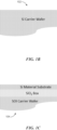
- FIGS. 1A-1C are cross-sectional views of examples 100, 102, and 104 of a carrier wafer.
- a donor wafer may also be referred to herein as a transfer wafer
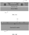
- the introduced fabrication technique involves wafer bonding of at least two wafers: a donor (transfer) wafer, and a carrier wafer.
- the donor wafer is a substrate wafer with the high quality photosensitive material layers to be transferred.
- the carrier wafer is a substrate wafer to which the desired transfer material is be transferred.
- the term "donor wafer” and “carrier wafer” are used in a relative sense. It is possible to combine the pre-PD wafer bonding techniques (e.g., pre-PD homogeneous wafer bonding or pre-PD heterogeneous wafer bonding) with other suitable wafer bonding techniques (e.g., the post-PD wafer bonding) introduced here; therefore, there may exist multiple carriers wafers if multiple wafer bonding steps are implemented in a certain application.
- the prepared carrier wafer 100 is a silicon (Si) wafer.
- the carrier wafer 100 can be doped with N-type dopants 110 at the surface of the wafer 100.
- the doped layer 110 can be accomplished by various known methods, such as implantation, or in-situ doping and diffusion.
- the carrier wafer may not be doped with impurities, such as the carrier wafer 102 shown in FIG. 1B .
- the carrier wafer 104 may be of a silicon-on-insulator (SOI) type.
- SOI silicon-on-insulator
- FIGS. 2A-2B are example processes that can be performed on a donor wafer 200 for forming photosensitive materials 210 on the donor wafer 200.
- the donor wafer 200 includes an optional separation layer 220 within the Si donor wafer 200.
- the exact depth of the separation layer 220 may vary according to the PD design.
- the separation layer 220 may be created by, for example, hydrogen implantation and/or impurity implantation.
- the doping profile of the donor wafer 200 can be customized to a specific PD design. Note that if a hydrogen implantation approach is used to form the separation layer 220, then the hydrogen implantation approach should be applied after the photosensitive materials are formed.
- the photosensitive material layer 210 that contains the main target of the transfer can be formed by epitaxial growth.
- the photosensitive material includes germanium (Ge).
- the Ge layer 210 can be formed by blanket epitaxy growth or selective epitaxy growth.
- a direct epitaxial growth of Ge on top of Si may result in a defect layer 212 high in threading dislocation density (TDD) due to a 4% lattice mismatch between Si and Ge materials.
- This dense defect layer 212 is typically at least 30 nm in thickness. As the material continues to grow above the high TDD Ge layer 212, the Ge material quality typically improves significantly.
- the layers that are the actual target of the transfer in the photosensitive material layer 210 include a pure Ge layer 216 and two Si x Ge 1-x layers 214 and 218.
- the Si x Ge 1-x layers may be formed unintentionally by thermal-induced intermixing or intentionally for various purposes including, for example, as an etch/polish stop, a diffusion barrier, a TDD blocking layer, a quantum well, and/or for bandgap engineering purposes.
- the dimension and other properties of the photosensitive material layers 214, 216, and 218 may be configured according to the photodiode device design of choice.
- the epitaxially grown layer 210 may be annealed at a high temperature (e.g., between 700 °C to 900 °C) after the growth to improve crystal quality.
- a high temperature e.g., between 700 °C to 900 °C
- Si x Ge 1-x (where 0 ⁇ x ⁇ 1) layer naturally include the pure Ge layer; therefore, it should be understood that the term Si x Ge 1-x layer should encompass all Ge layers that are grown on Si.
- Si x Ge 1-x layers having different Si/Ge ratios are shown as different layers. Therefore, a person having ordinary skills in the art should understand that these layers are illustrated in a relative sense, and that there may not be an exact boundary between given two consecutive Si x Ge 1-x layers.
- the photosensitive material layer 210 include only one Si x Ge 1-x layer 214, but include a P doped Ge layer 215 between the Si x Ge 1-x layer 214 and the Ge layer 216.
- the Si x Ge 1-x film(s) may be doped to certain doping profiles according to desired device designs. It is noted that, in some variations, the high TDD Ge Layer 212 may not necessarily exist. In other variants, the separation layer 220 and the one or more Si x Ge 1-x layers may not be present.
- the photosensitive material layer 210 may be formed on or sourced from a germanium-on-insulator (GOI) wafer or a Ge substrate wafer.
- GOI germanium-on-insulator
- FIGS. 3A-3C are example processes that can be performed on the donor wafer for passivation bonding layer preparation.
- an amorphous Si layer 230 (“a-Si") is deposited on the Si x Ge 1-x film layer 218's surface as a passivation layer.
- the a-Si layer 230 is to be formed on the separately prepared Si x Ge 1-x layer 218's surface prior to the wafer bonding.
- Example thickness for this a-Si layer 230 can be from 20 nm to 2 ⁇ m. In one example, the thickness of the a-Si layer 230 is around 50 nm to 100 nm.
- other materials for the passivation layer 230 can include poly-crystalline Si, single-crystalline Silicon, or any suitable combination thereof.
- the formed TDD in this particular case would be located mainly inside the Si passivation layer 230 rather than the Ge photosensitive layer 210, and therefore the TDD formed here has a much less impact to the PD's performance compared to those defects located inside the Ge photosensitive layer 210.
- this a-Si layer 230 and the Si x Ge 1-x layer 218 can be both implanted with dopants, such as phosphorus (P), arsenic (As), antimony (Sb) for N-type dopants, or boron (B) for P-type dopants.
- dopants such as phosphorus (P), arsenic (As), antimony (Sb) for N-type dopants, or boron (B) for P-type dopants.
- the implantation depth of the dopants may vary as needed by the device design.
- the implanted dopants can be activated processes such as rapid thermal annealing (RTA). Note that the a-Si passivation layer 230 may change into poly-crystalline Si during doping activation.
- the smoothness of the top surface of the a-Si passivation layer 230 should be maintained for a successful wafer bonding process later.
- Other processes can also be performed to the donor wafer prior to the wafer bonding process to improve the material quality and/or enhance the wafer bonding process if needed.
- the bonding surface should be smooth for better wafer bonding results. These processes may include, but not limited to, impurity doping, wafer polishing, capping layer forming, laser annealing, and/or pattern etching.
- the bonding surface material layer 230 is deliberately selected to be of the same doping type as the surface layer 110 of the carrier wafer 100, that is, "N-type” a-Si layer 230 to "N-type” Si layer 110 bond.
- This type of bonding is desirable because high level of common type doping can prevent a photodiode depletion region (or "quasi-neutral region") from extending into the defective interface-layer, which is a main reason for the detrimental device leakage current to incur at the defect sites.
- the a-Si layer 230 may serve as a passivation layer for the Si x Ge 1-x material surface 218. This can generally reduce surface dangling bonds, thereby reducing device leakage current.
- the Si material is also more stable than the Si x Ge 1-x material (especially for high Ge contents), and therefore the technique introduced here changes the bonding interface from "Si x Ge 1-x to Si" to "Si to Si,” thereby simplifying the wafer bonding process as well as improving the bonding results.
- the bonding surface i.e., the resulting material interface layer after the bonding
- the bonding surface will not be in direct contact with the Si x Ge 1-x material layers that are critical to device performance, thereby reducing or avoiding common negative impacts to device performance, yield, and reliability, that are induced by interface layer bonded with heterogeneous materials.
- the a-Si layer 230 may be partially or entirely replaced by any semiconductor material that is not Si x Ge 1-x while possessing passivation effects to the Si x Ge 1-x surface.
- An example of such semiconductor material is gallium arsenide (GaAs) with lattice matched to Ge.
- FIGS. 3B and 3C show two additional examples.
- the carrier wafer is a Ge substrate wafer and there is no Si x Ge 1-x surface.
- the a-Si passivation layer 230 is formed on a N-doped Ge layer 219.
- the carrier wafer is a GOI wafer and there is no Si x Ge 1-x surface or separation layer.
- the a-Si passivation layer 230 is formed on a N-doped Ge layer 219.
- the buffered oxide (BOX) layer in the GOI wafer can serve as the separation layer. More specifically, in some examples, the BOX layer can serve as an etching stop layer during post-bonding material removal processes.
- there is no high TDD Ge layer 212 since there is no direct growth of Ge on Si.
- FIG. 4 is a cross-sectional view of an example 400 after a wafer bonding process that bonds the donor wafer 200 and the carrier wafer 100 together.
- the Si donor wafer 200 is flipped up-side-down, and then wafer bonded to the Si carrier wafer 100.
- both the donor wafer 200's bonding surface and the carrier wafer 100's bonding surface should be smooth for successful wafer bonding.
- material layers similar to the passivation layer 230 may be deposited on the surface of the carrier wafer 100 if needed.
- the wafer bonding process may include, but not limited to, dry wafer bonding, wet wafer bonding, chemical wafer bonding, direct bonding, plasma activated bonding, or surface activated bonding.
- a number of thermal or pressurized processes may be applied to enhance bonding strength of the wafers.
- the Si carrier wafer may be patterned before the bonding, depending on the design.
- the technique introduced above may correspond to a set of unique structure orientations that include: a layer of Si material (e.g., amorphous Si, poly-crystalline Si, single crystalline Si, or a combination thereof) between a single-crystalline Si x Ge 1-x layer and a single-crystalline Si material substrate; and/or a layer of semiconductor material that is not Si x Ge 1-x , between a single-crystalline Si x Ge 1-x layer and a single-crystalline Si material substrate.
- a layer of Si material e.g., amorphous Si, poly-crystalline Si, single crystalline Si, or a combination thereof
- FIG. 5 is a cross-sectional view of an example 500, which is the example 400 after a post-bonding material removal process.
- the Si substrate from the donor wafer 200 has been removed.
- Material removal may be accomplished by, for example, wafer splitting, chemical etching, chemical-mechanical-polish (CMP) or wafer lapping.
- the separation layer 220 (see FIG. 2A ) can function as a stop layer such that a faster but coarser-grain material removal process (e.g., CMP) can be first applied, and then a slower but finer-grain material removal process (e.g., chemical etching with high selectivity chemicals) can be used thereafter.
- CMP chemical-mechanical-polish
- the high TDD Ge layer 212 is also removed. This layer 212's removal is optional depending on the quality of the transfer film (e.g., generally, the photosensitive Si x Ge 1-x material layers 210). It is noted, nonetheless, that the ability to remove the high TDD Ge layer 212 can alleviate the leakage current issue of the PD devices, and therefore is considered one of the major benefits that the current technique provides.
- the Si x Ge 1-x layer 214 may be used as an etch/polishing stop layer.
- the Si x Ge 1-x 214 is removed, such as shown in FIG. 5 . Whether to remove this layer 214 depends on device design. In some implementations, the high TDD Ge layer 212 may be removed, for example, by applying laser annealing techniques to recover this highly defective region.
- FIGS. 6A-6B are examples of photodetectors fabricated with components that are formed using techniques introduced here. With the structure created in FIG. 5 , PD with high quality photosensitive materials and without the high TDD Ge layer 212 can be fabricated.
- an isolated “island” shape structure is etched on the example 500 to create the main photodiode structure for PD 600.
- P-type dopants are implanted into the top surface of the photodiode mesa forming a P Ge layer 610 for the P contact, thereby creating a P-I-N photodiode structure.
- a passivation layer 620 may be optionally applied to cover the PD 600's photodiode mesa.
- the passivation layer 620 can include, but not limited to, a-Si, poly-crystalline Si, single crystalline Si, silicon oxide, silicon nitride, aluminum oxide, or any combination thereof.
- a dielectric layer 630 is deposited and planarized.
- Contact vias 640 are then formed, filled with contact materials (e.g., metal).
- one or more anti-reflection coating (ARC) layers may be formed on top of PD 600 to improve quantum efficiency.
- the passivation layer 620 can be formed after the formation of the dielectric layer 630.
- the dielectric layer 630 can be formed, for example, either before or after the wafer bonding process described above. Note that, in these examples, the passivation layer 620 may not exist between the interface of dielectric layer 630 and the N-Si layer 110.
- FIG. 6B Shown in FIG. 6B is an alternative PD example 602 where the polarity of the photodiode is the opposite of PD 600.
- Other PD variants include different doping profiles and/or different layer structures within the transfer film.
- FIG. 7 is an alternative example process that can be performed on the donor wafer for form ing photosensitive materials on the donor wafer.
- the carrier wafer preparation steps are the same as those introduced in FIGS. 1A-1C .
- the photosensitive material growth steps are also similar to those introduced in FIGS. 2A-2B , but with some variations.
- this alternative process does not include the passivation layer formation steps that are introduced in FIGS. 3A-3C above.
- this alternative process proceeds directly to the wafer bonding and the layer transfer of Si x Ge 1-x films 710 to a separate Si material carrier wafer (e.g., carrier wafer 100).
- the Ge material layer structure 710 may include different layer material composition, impurity doping profile and impurity dopant species.
- the Si material donor wafer 700 may be of other types of wafer substrates, such as SOI wafers.
- the materials layers may be configured according to specific photodiode designs if needed.
- the Si x Ge 1-x films may be doped to specific doping profiles. Specific doping profiles may be used for purposes such as Ohmic contact formation, electric field control, and/or surface states passivation.
- the transfer Si x Ge 1-x film may consist of various Si x Ge 1-x layers with different "x" composition values. Such layers may have specific effects such as, but not limited to, diffusion block, quantum well, TDD propagation blocking, bandgap engineering, and/or etch stop.
- the top surface of the Si x Ge 1-x epitaxial layer is doped with N-type dopant to form an N-type Ge layer 719.
- the doping concentrations is ⁇ 5 ⁇ 10 18 cm -3 within a depth of about 10 nm to 200 nm.
- transferring high quality Si x Ge 1-x from a transfer carrier substrate to a separate Si material substrate via "wafer bonding" techniques may have an adverse impact on the resulting PD's dark current characteristics.
- wafer bonding approaches often result in a heterogeneous interface layer (typically only a few nanometers in thickness) between bonded materials.
- this heterogeneous interface layer is often found to contain elements such as oxygen and carbon. It may also contain any contaminants present on the wafer surfaces prior to bonding, such as oxidized materials, compounds. These contaminants are detrimental to device operation if found within the active region of semiconductor devices.
- the bonding interface where the heterogeneous interface layer is, is encompassed within high dopant concentration regions.
- the bonding surface of Si x Ge 1-x layers on wafer 700 and the surface of Si material carrier wafer 100 should not be of highly opposite doping polarity that can form an p-n junction.
- An p-n junction if formed by and at the heterogeneous bonding interface, can be severely detrimental to the device performance.
- Such p-n junction can be avoided if the heterogeneous bonding interface is buried (implanted) within high doping levels of the same dopant types, because then the photodiode active region will terminate prior to reaching the highly doped heterogeneous bonding interface.
- high opposite doping polarity is defined as both layers being doped with opposite dopant types at concentrations of > 1 ⁇ 10 17 cm -3 .
- the Si x Ge 1-x and Si material substrate surface are both doped as high N-type. As an alternative, they can be both doped as high P-type. In other examples, one of the two surfaces of Si x Ge 1-x and Si material substrate is doped high as N-type and the other surface is intrinsic or unintentionally doped by either dopant types at less than a doping concentration level of 1 ⁇ 10 17 cm -3 . Note that the high level of N-dopants may diffuse over the heterogeneous bonding interface in the fabrication steps that are after the wafer bonding process.
- one of the two surfaces of Si x Ge 1-x and Si material substrate is doped high as P-type and the other surface is intrinsic or unintentionally doped by either dopant types at less than a doping concentration level of 1 ⁇ 10 17 cm -3 .
- the high level of P-dopants may diffuse over the heterogeneous bonding interface in the fabrication steps that are after the wafer bonding process.
- FIG. 8 is a cross-sectional view of an alternative example 800 after a wafer bonding process, bonding the donor wafer 700 and the carrier wafer 100 together.
- the Si transfer wafer 700 is flipped up-side-down and wafer bonded to the Si carrier wafer 100.
- the Si carrier wafer 100's surface should be smooth for successful wafer bonding.
- the wafer bonding process may be achieved by, for example, dry wafer bonding, wet wafer bonding, chemical wafer bonding, direct bonding, plasma assisted wafer bonding, or surface activated bonding. Thermal processes may be applied to enhance bonding strength of the wafers.
- FIG. 9 is a cross-sectional view of the alternative example of FIG. 8 after a post-bonding material removal process.
- the Si substrate from the donor wafer 700 has been removed.
- Material removal may be accomplished by, for example, wafer splitting, chemical etching, chemical-mechanical-polish (CMP) or wafer lapping.
- CMP chemical-mechanical-polish
- the high TDD Ge layer 712 is also removed. This layer 712's removal may be optional depending on the quality of the transfer film. It is noted, nonetheless, that the ability to remove the high TDD Ge layer 712 can alleviate the leakage current issue of the PD devices, and therefore is considered one of the major benefits that the current technique provides.
- the Si x Ge 1-x layer 714 may be used as an etch/polishing stop layer.
- the Si x Ge 1-x 714 is removed, such as shown in FIG. 9 . Whether to remove this layer 714 depends on device design. In some implementations, the high TDD Ge layer 712 may be removed, for example, by applying laser annealing techniques to recover this highly defective region.
- the technique may serve as a simplified version of the FIGS. 1A-5 , and provide the benefits of (1) reduced leakage current (dark current) originated from the high threading dislocation defect density layer, which is originated from Ge and Si lattice mismatch during hetero-epitaxial Si x Ge 1-x material growth; (2) reduced photo-generated carrier recombination loss from the high threading dislocation defect density layer; (3) mitigated negative performance impact to photodiode from wafer bonding hetero-interface layer by encompassing the hetero-interface layer within high impurity dopants; and (4) improved dopant diffusion control within photodiode from reduced thermal budget as a result of the wafer bonded photodiode fabrication.
- reduced leakage current dark current originated from the high threading dislocation defect density layer, which is originated from Ge and Si lattice mismatch during hetero-epitaxial Si x Ge 1-x material growth
- reduced photo-generated carrier recombination loss from the high threading dislocation defect density layer (3) mitigated negative performance impact to photodio
- the technique introduced above may correspond to a unique structure that includes: the lacking of high TDD region within photodiode's Si x Ge 1-x layer; the hetero-interface layer due to wafer bonding is buried under high levels of dopant concentration ( > 1 ⁇ 10 17 cm -3 ); and the fabricated photodiode becomes located in between the transferred material film and the Si substrate material. In other words, the resulting photodiode is not completely confined within the transferred material film.
- FIGS. 10A-10C are an example flow for bonding a donor wafer and a carrier wafer after forming the photodetectors on the donor wafer.
- a high performance PD (or "multi-pass PD") includes one or more mirror structures for reflecting the incident light so as to create multiple passes of the incident light in the light absorption or photosensitive region of the PD.
- the mirror structure(s) can, therefore, generally increase the quantum efficiency of the PD.
- Some example HP-PD designs include, for example, a double mirror photonic lock PD, and single mirror multiple pass PD.
- HP-PD normal incidence high performance PD
- back side incidence design Due to process feasibility, a conventional, mirror-equipped PD may be inclined to adopt a back side incidence type of design (where light is incident from the back side of the wafer that carries the photodetector such that a reflective mirror can be formed on the front side of the photodetector).
- the back side incidence type PD is often limited in the spectrum range--the range is generally narrower because being limited by substrate absorption.
- SOI wafer semiconductor-on-insulator wafer.
- an SOI wafer is called for by the design of an HP-PD because the PD design may use the buried oxide (BOX) layer in the SOI wafer as a dielectric mirror.
- BOX buried oxide
- processing SOI wafers is generally more difficult in many semiconductor fabrication foundries due to reliability concerns, and hence having to use SOI wafers is not favorable for integration of normal incidence PDs and CMOS field effect transistors (FETs).
- a post-PD wafer bonding technique is introduced below.
- the disclosed HP-PD structure sand their associated technique can enable high performance PD designs with one or more mirror structures without the need to use SOI wafers.
- the technique introduced here utilizes a series of bulk substrate to implement high performance PD structures based on wafer-to-wafer bonding. Utilizing bulk semiconductor wafers instead of SOI wafers makes HP-PD designs easier to fit into mainstream CMOS processes. The aforementioned substrate absorption related issues for back side incidence HP-PDs can also be reduced or even avoided. Note that this technique is applicable to both discrete PDs and the integration of PDs and CMOS based ICs.
- a PD 1010 has been fabricated on a donor wafer 1000.
- an optional separation layer 1020 and then a photon-absorption layer 1030 are formed on the donor wafer 1000.
- the separation layer 1020 can be, for example, a different doping layer, a proton implanted layer, or any layer with etching selectivity or mechanical property difference with respect to the rest of the substrate.
- a metal mirror layer 1040 can be deposited on top of the Ge photon absorption layer 1030 as a single optical mirror or a portion of a reflective region (i.e., one or more mirror layers that function together as one composite mirror).
- an optional dielectric mirror layer 1045 can be formed in between the metal layer 1040 and the Ge photon absorption region 1030.
- the optional dielectric mirror layer 1045 can act as an additional optical mirror layer and function together with the metal mirror layer 1040 as a single reflective region.
- the donor wafer 1000 can be covered by a dielectric material (e.g., SiO 2 ) layer 1050, and then prepared (e.g., polished) for wafer bonding.
- the dielectric mirror layer 1045 may include a single layer of silicon dioxide, silicon nitride, amorphous silicon, or poly silicon.
- the dielectric mirror layer 1045 may include a multi-layer structure having a combination of the aforementioned materials.
- a distributed Bragg reflector (DBR) mirror can be used to replace the metal mirror 1040.
- DBR distributed Bragg reflector
- a carrier wafer 1002 is prepared (e.g., bonding layer 1060 formation followed by polishing, the bonding layer 1060's material including dielectric, metal, or other materials) for wafer bonding with one or more techniques described here.
- the optional bonding layer 1060 is preferably the same type of material and/or having the same doping profile as the layer 1050 for improved bonding results. For example, if a dielectric bonding process is used, then the bonding layer 1060 should include a dielectric layer. If a metal bonding process is used, then the bonding layer 1060 should include a metal layer. If a hybrid bonding process is used, then the bonding layer 1060 should be partially dielectric and partially metal. In some implementations, when hybrid bonding is used, at least a part of the metal layer 1040 can serve as an optical mirror, an electrical contact, or their combinations.
- the donor wafer 1000 and the carrier wafer 1002 are bonded together.
- the substrate layer of the donor wafer 1000 (which is originally beneath but now above the Ge absorption layer 1030) is at least partially removed, with its removal depth controlled by etching processes or marked by the optional separation layer 1020.
- a surface clean-up process such as wet-etching or CMP can be performed.
- a dielectric mirror 1070 is formed above the photosensitive material layer 1030.
- the resulting HP-PD 1004 is a front side incidence double mirror PD system, with one metal mirror 1040 and one dielectric mirror 1070.
- the two mirrors can enhance optical absorption by confining the incoming incident light.
- the resulting HP-PD 1004 can be a front side incidence single mirror (i.e., mirror 1040) multi-pass PD system if an ARC layer is coated instead of a dielectric mirror 1070.
- the carrier wafer 1002 can include electronic circuits such as an amplifier, an analog to digital convertor (ADC), a serial-to-parallel interface (SerDes), or a digital circuit such as encoder or decoder.
- ADC analog to digital convertor
- SerDes serial-to-parallel interface
- the resulting PD 1004 can be integrated with the electronic circuits. More examples of integration are provided and discussed below.
- FIGS. 11A-11E show an alternative example for bonding a donor wafer and a carrier wafer after form ing the photodetectors on the donor wafer.
- the first step FIG. 11A
- all the PD components 1010 and one side of the mirror 1040 are formed on the donor wafer 1000 before the wafer bonding.
- An optional separation layer 1020 is placed inside the substrate of the donor wafer 1000. The separation layer 1020 is located at the stopping position for the following substrate removal.
- the donor wafer 1000 that has the PD 1010 is flipped over and bonded to a carrier wafer 1002.
- a photodetector structure with a single crystalline donor substrate on the top of and overlapping with a single crystalline photosensitive material in the bonded wafer is a photodetector structure with a single crystalline donor substrate on the top of and overlapping with a single crystalline photosensitive material in the bonded wafer.
- the area of the single crystalline donor substrate is no smaller than the area of the single crystalline photosensitive material.
- the substrate of the donor wafer 1000 and the separation layer 1020 is removed.
- a second dielectric mirror 1070 is deposited on the top of the PD 1010 to form a light absorption cavity between the two mirrors 1040 and 1070.
- the resulting HP-PD is a front side incidence single mirror (i.e., mirror 1040) multi-pass PD system if there no second dielectric mirror 1070 is formed, such as illustrated in FIG. 11C .
- an ARC layer can be added onto the mirror 1040 to form a front side incidence multi-pass PD system.
- bond pads 1080 are opened for the following packaging processes.
- the bond pad formation approach shown in FIG. 11E is merely an example; other suitable approaches may apply.
- the single crystalline donor substrate can be Si.
- the photosensitive material can be Ge.
- a top contact area 1085 that is created for the PD 1010 can be Si, SiGe, or partially-doped Ge layer.
- the contact area 1085 of the Si or SiGe or partially-doped Ge layer can be larger than or overlapping the area of the Ge absorption layer, so that the Si, SiGe, or partially-doped Ge layer 1085 can partially be used as electrical contacts to provide the electrical field in the Ge absorption region. That is to say, the width of the top contact area 1085 can be larger than the width the Ge absorption layer 1030.
- an anti-reflection coating (ARC) layer can be deposited on top of the front side reflector (e.g., the dielectric mirror 1070).
- the bottom of the carrier wafer 1002 can be thinned as needed, for example, by etching or polishing. If the PD is a back side incidence PD, then an ARC layer can then be deposited on the back side (e.g., the carrier wafer's bottom) and the metal mirror 1040 can be replaced with an opening to allow incident light to travel through the opening into the photosensitive material.
- the electrical contact can be made on the bond pad 1080 from the donor side by etching through the now top surface of the bonded wafer, such as shown in FIGS. 10C and 11E . Additionally or alternatively, the electrical contact can be made by etching from the bottom surface of the bonded wafer, forming a TSV structure (e.g., in a manner similar to the TSV structure for the IC in FIG. 15B , discussed below).
- FIGS. 12A-12D show a process of forming two alternative examples of a photodetector with mirror structures.
- a front side incidence double mirror HP-PD such as the flow of FIGS. 10A-10C
- the flow of FIGS. 12A-12C can result in a back side incidence double mirror HP-PD.
- a single or double mirror system may be used for HP-PD; however, the incident light now comes from the bottom of the PD (i.e., from the carrier wafer 1202's bottom).
- the PD device 1210 and an optional dielectric mirror 1240 may be formed on a donor wafer 1200 and bonded to a carrier wafer 1202.
- a top contact area 1285 that is created for the PD 1210 can be Si, SiGe, or partially-doped Ge layer.
- the contact area 1285 of the Si or SiGe or partially-doped Ge layer can be larger than or overlapping the area of the Ge absorption layer, so that the Si, SiGe, or partially-doped Ge layer 1285 can partially be used as electrical contacts to provide the electrical field in the Ge absorption region. That is to say, the width of the top contact area 1285 can be larger than the width the Ge absorption layer 1230.
- FIG. 12D as an alternative example 1206 to having a double mirror structure as illustrated in FIG. 12C (i.e., mirrors 1240 and 1270), a single mirror structure can be implemented.
- the dielectric mirror 1240's function which is illustrated and discussed with respect to FIG. 12C , is not implemented in FIG. 12D (e.g., which can be a simple opening instead) and may allow light to pass directly from the backside of the carrier wafer 1202 into the photosensitive material 1230.
- the example 1206 constitutes a single mirror back-side incidence PD structure.
- an optional dielectric mirror layer 1275 that can be included between the metal mirror 1270 and the photosensitive material 1230.
- the dielectric mirror layer 1275 can function together with the metal mirror 1270 as a single composite mirror, which may improve and/or provide more process control over the overall mirror's reflectivity.
- the dielectric mirror layer 1275 may include a single layer of silicon dioxide, silicon nitride, amorphous silicon, or poly silicon.
- the dielectric mirror layer 1275 may include a multi-layer structure having a combination of the aforementioned materials.
- either an SOI or Si substrate may be used as the donor wafer.
- wafer-to-wafer dielectric bonding can be used in this structure.
- the separation layer 1220 can be, for example, a different doping layer, a proton implanted layer, or any suitable layer with etching selectivity or mechanical property difference with respect to the rest of the donor wafer 1200's substrate.
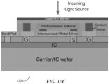
- FIGS. 13A-13C show an embodiment of a photodetector with mirror structures and integrated circuits (ICs).
- the front side incidence double mirror HP-PD on a donor wafer 1300 is bonded to a carrier wafer 1302 that includes a CMOS IC 1390.
- the IC 1390 includes at least one CMOS transistor that is fabricated on the carrier wafer 1302.
- the PD 1310 is fabricated on the donor wafer 1300.
- a wafer-to-wafer hybrid bond process metal-plus-dielectric bond
- the electrical connection between the PD 1310 and the IC 1390 can be implemented by metal bonding. This technique can be applied in a similar way for a back side incidence single or double mirror HP-PD.
- FIG. 14 shows yet another alternative embodiment 1404 that includes a through-silicon via 1492 (TSV) formed on the carrier wafer 1402.
- TSV through-silicon via 1492
- the IC circuit 1490's output is connected to the TSV 1492 on the side of the carrier wafer 1402. This technique can be applied in a similar way for a back side incidence single or double mirror HP-PD.
- FIGS. 15A-15B show two example schemes of integration of front side incidence double mirror photodetectors and integrated circuits.
- a double mirror PD is shown in the figures, these techniques are generally applicable to a single mirror PD, for example, by eliminating the top mirror between the photosensitive material and the light source.
- a double mirror system including HP-PD 1510 is shown here as an example.
- An IC 1590 is integrated to the PD 1510 on the same wafer using the techniques introduced here.
- the IC 1510's output is connected to a bond pad 1580
- the IC 1510's output is connected to a TSV 1592 on carrier wafer side.
- these integration techniques introduced here are not limited to any specific kind of PD system; they can be applied in a similar way for other PD system including, for example, a back side incidence double mirror HP-PD, or a single mirror HP-PD.
- FIGS. 16A-16B show two alternative example schemes of integration, with integrated circuits bonded on front side incidence double mirror photodetectors.
- the double mirror system is shown here as an example, and the PD 1610 is bonded on the carrier wafer 1602 using the techniques disclosed here.
- the IC 1690 is then bonded on the PD structure via a flip-chip bonding process.
- the flip-chip bonding process can be either chip-to-chip or chip-to-wafer.
- the IC 1690's output is connected to bond pads 1680 via solder balls, copper (Cu) pillars 1694, or other similar techniques.
- the IC 1690's output is connected to a TSV 1692 on the IC's wafer 1606.
- FIGS. 17A-17B show two alternative example schemes of integration, with back side incidence photodetectors bonded on integrated circuits.
- FIGS. 17A-17B utilize a back side incidence HP-PD design (which can be, for example, single or double mirror), which is bonded onto the carrier wafer 1702.
- the PD 1710 is then diced into chips and bonded on the IC 1790 via a flip-chip bonding process.
- the IC 1790's output is connected to a bond pad 1780 on IC side, which can be suitable for making electrical contact to other chips or printed circuit boards (PCBs).
- PCB printed circuit boards
- the IC 1790's output is connected to a TSV 1792 on the IC's wafer 1706.
- FIGS. 18A-18B show two additional examples of front side incidence single mirror photodetectors and their integration applications.
- the examples shown in FIGS. 18A-18B utilize a front side incidence single mirror system for the HP-PD design.
- Shown in FIG. 18A is a discrete PD 1810, in which the HP-PD is directly bonded to a carrier wafer 1802.
- Shown in FIGS. 18B is an integration application of PD and IC, where the PD 1810 and IC 1890 are integrated on the same wafer, and then bonded on the carrier wafer 1802.
- a dielectric layer that is located between a photosensitive materials and the initial light incidence source and acts as a mirror to partially transmit the incident light and partially reflect the light reflected by another mirror.
- back side incidence and front side incidence are relative terms, typically used to describe where light is incident from relative to the PD device.
- back side incidence and front side incidence are used based on the optical path of the incident light relative to the positions of carrier and donor wafers.
- such terms used here may take reference to a particular PD's overall design, regardless of the actual existence of the donor wafer or the carrier wafer at the time of a particular described operation. Consequently, for example, if a PD's optical path of the incident light signal by design encounters the donor wafer prior to the carrier wafer, then the device may be referred to as a "front side incidence” type PD.
- the device may be referred to as a "back side incidence” type PD. It is worth noting that this usage may be different from the conventional notion of a "front side incidence” or a “back side incidence” photodetector, because conventional PD structures are not multi-wafer based.
- an ARC layer or/and a lens structure may be included between the photo-sensitive materials and the initial light incidence source, or alternatively, between a dielectric partial mirror and the initial light incidence source if such dielectric partial mirror is included.
- the lens structure can be a curved silicon surface formed by etching, a number of polymer based materials shaped into a curved structure, or a number of photonic crystal structures with multiple layers of silicon and dielectric.
- the lens structure may be hemisphere-like.
- the lens structure may be photonic crystal-like, in which multiple holes, recesses, rods, rings, mesas are arranged inside.
- the lens can be made of suitable materials including, for example, crystalline, polymeric, organic or inorganic materials.
- a high speed hybrid waveguide-based multiple channel optical transceiver module may be further implemented.
- a receiver module can include normal incidence PDs bonded to a waveguide-based multiple channel passive system.
- Pulse-amplitude modulation (PAM) or other modulation schemes can be used to boost up the communication speed.
- a transmitter module can also be implemented by replacing the PDs introduced above with vertical-cavity surface-emitting laser (VCSEL) diodes.
- VCSEL vertical-cavity surface-emitting laser
- FIG. 19 shows a cross-sectional view of a waveguide structure 1900 that can be utilized with the photodetectors introduced here.
- the waveguide structure 1900 is implemented on an SOI wafer 1902.
- the SOI wafer 1902 includes a buried oxide (BOX) layer 1910.
- the silicon (Si) on the SOI wafer 1902 has been patterned to include Si waveguide 1920 and couplers 1930. Additionally, a bond pad 1980 is formed on a portion of the Si waveguide 1920.
- the drawings are provided here for illustration purposes, and that other forms of optical components (such as other types of optical couplers) can be applicable.
- FIG. 20 shows an example schematic of a waveguide receiver system 2000 embodying one or more techniques introduced here.
- the waveguide receiver system 2000 includes the waveguide structure 1900, as well as a fiber 2010 coupled to one of the couplers 1930.
- the waveguide receiver system 2000 also includes a front side incidence PD 2020 flip-chip bonded to the bonding pad 1980 and coupled to another one of the couplers 1930.
- the PD 2020 is positioned to receive and detect the optical signals transmitted from the fiber 2010.
- a direct fiber to waveguide coupling approach can be used to reduce the coupling loss from the waveguide to the fiber coupler.
- the waveguide receiver system 2000 includes an integrated circuit (IC) 2090, also bonded to the bond pad 1980 through wire bonding as shown in FIG. 20 or through flip-chip bonding (not shown for simplicity).
- the IC 2090 is configured to process the output from the PD 2020.
- the IC 2090 can be integrated with the PD 2020 on the same chip using techniques introduced previously.
- FIG. 21 shows an example schematic of another waveguide system 2100 exemplifying one or more techniques introduced here.
- system 2100 includes a back side incidence HP-PD 2025 (e.g., a single or double mirror PD).
- HP-PD 2025 is bonded to the ponding pad 1980.
- Light signals are directed into the in-plane Si waveguide system 2100 though couplers 1930.
- Light signals travel in the Si waveguides 1900 and, in some examples, can split into multiple channels through a splitter such as demultiplexer (DeMUX). Each channel of light can be then re-directed out-of-plane to the bonded PD 2025 for signal collection. More examples of the multi-channel application are discussed in FIGS. 22A-22B .
- the extracted electrical signals from the PD 2025 are sent to the IC 2190.
- the signal can be transferred through bond wire or flip-chip bonding pad.
- the IC 2190 is wire bonded to another side of the HP-PD 2025.
- the IC 2190 is configured to process the output from the PD 2025.
- FIGS. 22A-22B show examples of multi-channel receiver modules that can be realized with examples of the present disclosure.
- Advantages of utilizing a waveguide-based wavelength-division multiplexing (WDM) system as disclosed here can include reduced fiber cost compared to traditional, non-WDM systems, noting that the fiber cost typically is a major factor for mid-to-long-range applications.
- WDM wavelength-division multiplexing
- FIG. 22A Shown in FIG. 22A is a top view of a dual-channel Si waveguide passive system 2200 with a DeMUX 2210 , an Si waveguide 2220 and couplers 2230.
- Two 25 Gbps PDs 2240 are bonded on the top of their respective couplers 2230 (obscured by the PDs 2240) to enable a 50 Gbps receiver module.
- the bandwidth of the receiver module can be boosted up to 100 Gbps.
- the PDs 2240 can be single or double mirror PDs.
- the target wavelength is single mode near 1310 nm or single mode near 1550 nm.
- FIG. 22B Shown in FIG. 22B is a top view of a quad-channel Si waveguide passive system 2205 with a DeMUX 2215, an Si waveguide 2225 and couplers 2235.
- PDs 2245 are bonded on the top of their respective couplers 2235 to enable a 100 Gbps receiver module.
- the receiver module's bandwidth can be boosted up to 200 Gbps.
- Other PAM schemes such as PAM-8, PAM-16, and so forth, or other modulation and encoding/decoding schemes may also be applicable.
Description
- Embodiments of the present disclosure relate to semiconductor device design, and more particularly, to multi-wafer based semiconductor photodetectors and other devices.
- Fueled by big data, cloud computing, as well as other computer network and telecommunication applications, there is an ever increasing demand for high speed telecommunication means. High speed optical transmitters and receivers (or collectively referred to herein as "transceivers") that are capable of exceeding a transmission rate of 25 Gbps have attracted the public's attention.
- While optical transceivers are gaining popularity, semiconductor photodetector (PD) design and manufacturing technology is often different and sometimes even incompatible with other kinds of traditional semiconductor device manufacturing technologies, such as those for metal oxide semiconductor (MOS) transistors. As an example, a direct growth of silicon germanium (SiGe) materials on silicon material substrates can often cause a defect layer, laden with lattice mismatch between Ge and Si. This defect layer can result in leakage current and degraded PD performance characteristics (e.g., signal-to-noise ratio (SNR)).
- It is beneficial to have improved device design and fabrication techniques that enable PDs and/or other electronic circuits using typical semiconductor device manufacturing technologies meanwhile reducing the adverse impacts on PDs' performance.
- LI CHENG ET AL: "SiGe/Si resonant-cavity-enhanced photodetectors for 1.3 µm operation fabricated using wafer bonding techniques", JOURNAL OF APPLIED PHYSICS, vol. 92, no. 3, August 2002, p.1718-1720 discloses SiGe/Si resonant-cavity-enhanced photodetectors for 1.3 µm operation fabricated using wafer bonding techniques.
M.K. Emsley ET AL: "Silicon substrates with buried distributed Bragg reflectors for resonant cavity-enhanced optoelectronics ",IEEE JOURNAL OF SELECTED TOPICS IN QUANTUM ELECTRONICS., vol. 8, no. 4, July 2002, p. 948-955, discloses Silicon substrates with buried distributed Bragg reflectors for resonant cavity-enhanced optoelectronics.
Ashok K. Sood ET AL: "Development of SiGe arrays for visible-near IR applications", Proceedings of SPIE, vol. 7780, 17 August 2010, p.77800F1-10 discloses SiGe arrays for visible-near IR applications.
Jian Wang ET AL: "Ge-Photodetectors for Si-Based Optoelectronic Integration", Sensors, vol. 11, no. 12, 12 January 2011, p. 696-718 discloses Ge-Photodetectors for Si-Based Optoelectronic Integration.
The present invention provides a multi-wafer based semiconductor light absorption structure as set out in claim 1. Further aspects of the present invention are set out in the remaining claims. - One or more embodiments of the present disclosure are illustrated by way of example and not limitation in the figures of the accompanying drawings, in which like references indicate similar elements. These drawings are not necessarily drawn to scale.
-
FIGS. 1A-1C are cross-sectional views of examples of a carrier wafer. -
FIGS. 2A-2B are example processes that can be performed on a donor wafer (also referred to as a transfer wafer) for forming photosensitive materials on the donor wafer. -
FIGS. 3A-3C are example processes that can be performed on the donor wafer for passivation bonding layer preparation. -
FIG. 4 is a cross-sectional view of an example after a wafer bonding process, bonding the donor wafer and the carrier wafer together. -
FIG. 5 is a cross-sectional view of an example after a post-bonding material removal process. -
FIGS. 6A-6B are examples of photodetectors fabricated with components that are formed using techniques introduced here which are useful for understanding the invention but not covered by the scope of the claims. -
FIG. 7 is an alternative example process that can be performed on the donor wafer for forming photosensitive materials on the donor wafer. -
FIG. 8 is a cross-sectional view of an alternative example after a wafer bonding process, bonding the donor wafer and the carrier wafer together. -
FIG. 9 is a cross-sectional view of the alternative example ofFIG. 8 after a post-bonding material removal process. -
FIGS. 10A-10C are an example flow for bonding a donor wafer and a carrier wafer after forming the photodetectors on the donor wafer, which is useful for understanding the invention but not covered by the scope of the claims. -
FIGS. 11A-11E show an alternative example for bonding a donor wafer and a carrier wafer after forming the photodetectors on the donor wafer, which is useful for understanding the invention but not covered by the scope of the claims. -
FIGS. 12A-12D show a process of forming two alternative examples of a photodetector with mirror structures, which are useful for understanding the invention but not covered by the scope of the claims. -
FIGS. 13A-13C show an embodiment according to the present invention of a photodetector with mirror structures and integrated circuits (ICs). -
FIG. 14 shows yet another alternative embodiment that includes a through-silicon via (TSV) formed on the carrier wafer. -
FIGS. 15A-15B show two example schemes of integration of front side incidence double mirror photodetectors and integrated circuits, which are useful for understanding the invention but not covered by the scope of the claims. -
FIGS. 16A-16B show two alternative example schemes of integration, with integrated circuits bonded on front side incidence double mirror photodetectors. -
FIGS. 17A-17B show two alternative example schemes of integration, with back side incidence photodetectors bonded on integrated circuits. -
FIGS. 18A-18B show two additional examples of front side incidence single mirror photodetectors and their integration applications. -
FIG. 19 shows a cross-sectional view of a waveguide structure that can be utilized with the photodetectors introduced here. -
FIG. 20 shows an example schematic of a waveguide system embodying one or more techniques introduced here. -
FIG. 21 shows an example schematic of another waveguide system embodying one or more techniques introduced here. -
FIGS. 22A-22B show examples of multi-channel receiver modules that can be realized with embodiments of the present disclosure. - Germanium (Ge) based or silicon germanium (SiGe) based optical sensors (e.g., photodetectors or photodiodes (generally referred to as PD herein), avalanche photodiodes (APD), or image sensors) have long been applauded for their better sensitivity to near infra-red (NIR) wavelength optical signals. In addition, SiGe based material systems are relatively compatible to contemporary, high volume complementary metal oxide semiconductor (CMOS) manufacturing technologies, and therefore the integration potentials with integrated circuits of such material systems are much favored. With the advancement in Ge epitaxy technology, direct growth of SixGe1-x (where 0 ≤ x < 1) materials on silicon (Si) material substrates have become popular. (Note that SixGe1-x (where 0 ≤ x < 1) here includes all suitable SiGe composition combinations from 100% Ge to almost 100% Si.)
- However, it is observed that, due to a large lattice mismatch (i.e., about 4%) between Ge and Si, a dense defect layer typically can form near the interface of the Si substrate and deposited SixGe1-x film to relax the strain energy generated from this large lattice mismatch. This dense defect layer is typically at least 30 nm in thickness and is highly dependent on the Ge content of the film. The large number of defects can act as carrier generation and recombination centers if these defects are located within or close to the electrical fields or intrinsic regions of the PD devices, which can severely increase the leakage current of such devices. This leakage current in PD, also known as the "dark current," is a major source of noise current for PDs that can severely degrade a photodetector's signal-to-noise (SNR) ratio. This relatively high threading dislocation density (TDD) issue makes Ge or SixGe1-x based photodiodes' dark current characteristics inferior when compared to competing photodiode materials systems such as pure silicon and III-V materials (e.g., GaAs or InGaAs). The magnitude of dark current have been shown to be positively correlated with the TDD. Furthermore, the high TDD layer has been observed to be horizontally conductive, posing detrimental effects to device performance if the direction of the device's primary current flow coincided with the horizontal direction of the high TDD layer. There has been attempts to use germanium substrate wafers to form the high quality germanium material layer that is to be transferred to other wafers. Yet, generally speaking, germanium substrate wafers are expensive, limited in size and difficult to handle due to its fragile nature, therefore making such approach difficult to scale for production.
- Accordingly, introduced here are a number of device design and fabrication techniques that enable PDs and/or other electronic circuits using typical semiconductor device manufacturing technologies meanwhile reducing the adverse impacts on PDs' performance. Examples of the various techniques introduced here include, but not limited to, a pre-PD homogeneous wafer bonding technique, a pre-PD heterogeneous wafer bonding technique, a post-PD wafer bonding technique, a number of multi-stack PD device structures, as well as other structures and techniques related to integration and optoelectronic-related applications. With the introduced techniques, it is possible to fabricate PDs and/or other electronic circuits using typical semiconductor device manufacturing technologies, such as direct growth of SixGe1-x on Si substrate, while reducing the adverse impacts of the leakage current caused by the dense defect layer on PDs' performance.
- In the following description, the example of a Si/SiGe material system PD is used, for illustrative purposes only, to explain various techniques that can be implemented for manufacturing the PD using typical direct growth material epitaxy technology while reducing the adverse impact of the defect layer at the material interface caused by lattice mismatch. Note, however, that the techniques introduced here are not limited in applicability to any particular kind of PD and/or transistors. For example, even though one or more figures introduced in connection with the techniques disclosed here (e.g.,
FIGS. 10A-10C ,15A-15B , and16A-1 6B ) illustrate a front side incidence double mirror PD structure, the techniques are applicable in a similar manner to other types of PD structure including, but not limited to, a single mirror PD structure, a back side incidence PD. - For purposes of discussion herein, a PD is a semiconductor apparatus that converts an optical signal into a photo-generated electrical signal. Examples of PD devices include a P-I-N photodiode, an avalanche photodiode (APD), a uni-traveling carrier photodiode, or an image sensor (including, for example, a near-infrared (NIR) sensor). A typical P-I-N diode includes two highly-doped semiconductor layers with opposite electrical polarity (i.e., one "p-type" and one "n-type") and a photon absorption layer (i.e., "intrinsic") sandwiched in between the two layers. In the context of P-I-N PDs, the term "highly-doped" typically may be understood as having a doping concentration above 1018 cm-3; the term "intrinsic" typically may be understood as having a doping concentration below 1017 cm-3 in SixGe1-x material systems.
- Further, in the following description, numerous specific details are set forth to provide a thorough understanding of the present disclosure. It will be apparent to one skilled in the art that the techniques introduced here may be practiced without these specific details. In other instances, well-known features, such as specific fabrication techniques, are not described in detail in order to not unnecessarily obscure the present disclosure. References in this description to "an embodiment," "one embodiment," or the like, mean that a particular feature, structure, material, or characteristic being described is included in at least one embodiment of the present disclosure. Thus, the appearances of such phrases in this specification do not necessarily all refer to the same embodiment. On the other hand, such references are not necessarily mutually exclusive either. Also, it is to be understood that the various exemplary embodiments shown in the figures are merely illustrative representations and are not necessarily drawn to scale.
- The terms "coupled" and "connected," along with their derivatives, may be used herein to describe structural relationships between components. It should be understood that these terms are not intended as synonyms for each other. Rather, in particular embodiments, "connected" may be used to indicate that two or more elements are in direct physical or electrical contact with each other. Unless otherwise made apparent in the context, the term "coupled" may be used to indicate that two or more elements are in either direct or indirect (with other intervening elements between them) physical or electrical contact with each other, and/or that the two or more elements co-operate or interact with each other (e.g., as in a cause and effect relationship).
- The terms "over," "under," "between," and "on" as used herein refer to a relative position of one material layer with respect to other material layers. As such, for example, one layer disposed "over" or "under" another layer may be directly in contact with the other layer or may have one or more intervening layers. Moreover, one layer disposed "between" two layers may be directly in contact with the two layers or may have one or more intervening layers. In contrast, a first layer "on" a second layer is in contact with that second layer. Additionally, the relative position of one layer with respect to other layers is provided assuming operations are performed relative to a substrate without consideration of the absolute orientation of the substrate. The term "atop" means "on the top of."
- Similarly, the terms "above" and "below" are generally used herein for describing the relative physical location of different devices, layers, sections, portions, etc., with respect to their shortest distances to the semiconductor substrate. For example, a first layer "above" a second layer means that, when measured from the substrate at the same horizontal level, the first layer is farther away in distance from the substrate than the second layer. Conversely, a first layer "below" a second layer means that, when measured from the substrate at the same horizontal level, the first layer is closer in distance from the substrate than the second layer. As used herein, "horizontal" means parallel to the planar surface of the substrate, such as the horizontal axis 101 illustrated in
FIG. 1A . - The terms "front side" and "back side" are used in a relative sense, from the perspective of an individual object that the terms modify or otherwise describe. As such, the terms "front side" and "back side" do not indicate an absolute direction; rather, the direction being referred to depends on the object that the term "front side" or "back side" modifies. For example, a "back side" of a donor wafer (e.g., wafer 100,
FIG. 1A ) may eventually become a "front side" of the resulting PD structure (e.g., structure 400,FIG. 4 ). - The term "immediately" or "directly" may be construed as "in physical contact," as will be made apparent by the context; for example, unless contradictory to the context, a first layer "immediately above" or "directly above" a second layer means that the first layer is above and in physical contact with the second layer.
- As used herein, "contact plug," "contact via," or simply "contact" for a device refers to any substantially vertical wire between with the doped regions for the device and the first interconnect layer for the device. The term "interconnect" refers to any substantially horizontal wire between devices for inter-device signal transmission/communication. The "first" interconnect layer refers to the lowest interconnect layer. Notably, with the techniques introduces here, the first interconnect layer is device specific; that is to say, in some embodiments, the first interconnect for one device may be different than that for another device, even when both devices are fabricated on the same wafer.
-
FIGS. 1A-1C are cross-sectional views of examples 100, 102, and 104 of a carrier wafer. To reduce or even completely avoid the aforementioned leakage current issue caused by the dense defect layer, one approach is to first prepare high quality SixGe1-x on a substrate of a donor wafer (may also be referred to herein as a transfer wafer), and then transfer the high quality material to a separate Si material substrate via "wafer bonding" to a carrier wafer. The introduced fabrication technique involves wafer bonding of at least two wafers: a donor (transfer) wafer, and a carrier wafer. The donor wafer is a substrate wafer with the high quality photosensitive material layers to be transferred. The carrier wafer is a substrate wafer to which the desired transfer material is be transferred. Note that the term "donor wafer" and "carrier wafer" are used in a relative sense. It is possible to combine the pre-PD wafer bonding techniques (e.g., pre-PD homogeneous wafer bonding or pre-PD heterogeneous wafer bonding) with other suitable wafer bonding techniques (e.g., the post-PD wafer bonding) introduced here; therefore, there may exist multiple carriers wafers if multiple wafer bonding steps are implemented in a certain application. - In
FIG. 1A , the prepared carrier wafer 100 is a silicon (Si) wafer. The carrier wafer 100 can be doped with N-type dopants 110 at the surface of the wafer 100. The doped layer 110 can be accomplished by various known methods, such as implantation, or in-situ doping and diffusion. In one or more examples, the carrier wafer may not be doped with impurities, such as the carrier wafer 102 shown inFIG. 1B . Alternatively, as shown inFIG. 1C , the carrier wafer 104 may be of a silicon-on-insulator (SOI) type. Each carrier wafer can be doped differently, in terms of the doping profile and the impurity type, according to a desired photodiode design. -
FIGS. 2A-2B are example processes that can be performed on a donor wafer 200 for forming photosensitive materials 210 on the donor wafer 200. - In the example shown in
FIG. 2A , the donor wafer 200 includes an optional separation layer 220 within the Si donor wafer 200. The exact depth of the separation layer 220 may vary according to the PD design. The separation layer 220 may be created by, for example, hydrogen implantation and/or impurity implantation. The doping profile of the donor wafer 200 can be customized to a specific PD design. Note that if a hydrogen implantation approach is used to form the separation layer 220, then the hydrogen implantation approach should be applied after the photosensitive materials are formed. - Then, the photosensitive material layer 210 that contains the main target of the transfer can be formed by epitaxial growth. In this example, the photosensitive material includes germanium (Ge). The Ge layer 210 can be formed by blanket epitaxy growth or selective epitaxy growth. As discussed above, a direct epitaxial growth of Ge on top of Si may result in a defect layer 212 high in threading dislocation density (TDD) due to a 4% lattice mismatch between Si and Ge materials. This dense defect layer 212 is typically at least 30 nm in thickness. As the material continues to grow above the high TDD Ge layer 212, the Ge material quality typically improves significantly.
- In accordance with a number of examples, the layers that are the actual target of the transfer in the photosensitive material layer 210 include a pure Ge layer 216 and two SixGe1-x layers 214 and 218. The SixGe1-x layers may be formed unintentionally by thermal-induced intermixing or intentionally for various purposes including, for example, as an etch/polish stop, a diffusion barrier, a TDD blocking layer, a quantum well, and/or for bandgap engineering purposes. The dimension and other properties of the photosensitive material layers 214, 216, and 218 may be configured according to the photodiode device design of choice. Additionally, the epitaxially grown layer 210 may be annealed at a high temperature (e.g., between 700 °C to 900 °C) after the growth to improve crystal quality. Note that the definition of SixGe1-x (where 0 ≤ x < 1) layer naturally include the pure Ge layer; therefore, it should be understood that the term SixGe1-x layer should encompass all Ge layers that are grown on Si. However, for purposes of easier illustration, SixGe1-x layers having different Si/Ge ratios are shown as different layers. Therefore, a person having ordinary skills in the art should understand that these layers are illustrated in a relative sense, and that there may not be an exact boundary between given two consecutive SixGe1-x layers.
- In the example of donor wafer 202 shown in
FIG. 2B , the photosensitive material layer 210 include only one SixGe1-x layer 214, but include a P doped Ge layer 215 between the SixGe1-x layer 214 and the Ge layer 216. As discussed, the SixGe1-x film(s) may be doped to certain doping profiles according to desired device designs. It is noted that, in some variations, the high TDD Ge Layer 212 may not necessarily exist. In other variants, the separation layer 220 and the one or more SixGe1-x layers may not be present. Additionally or alternatively, there may be more than one SixGe1-x layer of various "x" values present, and/or the SixGe1-x layer may be a film of continuously graded "x" value. In yet some other examples, the photosensitive material layer 210 may be formed on or sourced from a germanium-on-insulator (GOI) wafer or a Ge substrate wafer. -
FIGS. 3A-3C are example processes that can be performed on the donor wafer for passivation bonding layer preparation. - In the example shown in
FIG. 3A , an amorphous Si layer 230 ("a-Si") is deposited on the SixGe1-x film layer 218's surface as a passivation layer. Specifically, the a-Si layer 230 is to be formed on the separately prepared SixGe1-x layer 218's surface prior to the wafer bonding. Example thickness for this a-Si layer 230 can be from 20 nm to 2µm. In one example, the thickness of the a-Si layer 230 is around 50 nm to 100 nm. Besides a-Si, other materials for the passivation layer 230 can include poly-crystalline Si, single-crystalline Silicon, or any suitable combination thereof. Note that depositing single or poly crystalline Si passivation layers over Ge could as well lead to TDD formation due to the 4% lattice mismatch. However, the formed TDD in this particular case would be located mainly inside the Si passivation layer 230 rather than the Ge photosensitive layer 210, and therefore the TDD formed here has a much less impact to the PD's performance compared to those defects located inside the Ge photosensitive layer 210. - Furthermore, this a-Si layer 230 and the SixGe1-x layer 218 can be both implanted with dopants, such as phosphorus (P), arsenic (As), antimony (Sb) for N-type dopants, or boron (B) for P-type dopants. The implantation depth of the dopants may vary as needed by the device design. The implanted dopants can be activated processes such as rapid thermal annealing (RTA). Note that the a-Si passivation layer 230 may change into poly-crystalline Si during doping activation.
- After the passivation layer 230 is formed atop of the photosensitive material layer 210, the smoothness of the top surface of the a-Si passivation layer 230 should be maintained for a successful wafer bonding process later. Other processes can also be performed to the donor wafer prior to the wafer bonding process to improve the material quality and/or enhance the wafer bonding process if needed. For example, according to one or more embodiments, the bonding surface should be smooth for better wafer bonding results. These processes may include, but not limited to, impurity doping, wafer polishing, capping layer forming, laser annealing, and/or pattern etching.
- With simultaneous reference to
FIG. 1A , in the example shown inFIG. 3A , the bonding surface material layer 230 is deliberately selected to be of the same doping type as the surface layer 110 of the carrier wafer 100, that is, "N-type" a-Si layer 230 to "N-type" Si layer 110 bond. This type of bonding is desirable because high level of common type doping can prevent a photodiode depletion region (or "quasi-neutral region") from extending into the defective interface-layer, which is a main reason for the detrimental device leakage current to incur at the defect sites. - There are several advantages of this passivation layer formation introduced here. It has been demonstrated that device leakage current can be reduced by applying passivating materials to SixGe1-x surface. Here, the a-Si layer 230 may serve as a passivation layer for the SixGe1-x material surface 218. This can generally reduce surface dangling bonds, thereby reducing device leakage current. The Si material is also more stable than the SixGe1-x material (especially for high Ge contents), and therefore the technique introduced here changes the bonding interface from "SixGe1-x to Si" to "Si to Si," thereby simplifying the wafer bonding process as well as improving the bonding results. In addition, the bonding surface (i.e., the resulting material interface layer after the bonding) will not be in direct contact with the SixGe1-x material layers that are critical to device performance, thereby reducing or avoiding common negative impacts to device performance, yield, and reliability, that are induced by interface layer bonded with heterogeneous materials.
- In some alternative examples, the a-Si layer 230 may be partially or entirely replaced by any semiconductor material that is not SixGe1-x while possessing passivation effects to the SixGe1-x surface. An example of such semiconductor material is gallium arsenide (GaAs) with lattice matched to Ge.
-
FIGS. 3B and 3C show two additional examples._ InFIG. 3B , the carrier wafer is a Ge substrate wafer and there is no SixGe1-x surface. Instead, the a-Si passivation layer 230 is formed on a N-doped Ge layer 219. InFIG. 3C , the carrier wafer is a GOI wafer and there is no SixGe1-x surface or separation layer. Similar to the example shown inFIG. 3B , the a-Si passivation layer 230 is formed on a N-doped Ge layer 219. The buffered oxide (BOX) layer in the GOI wafer can serve as the separation layer. More specifically, in some examples, the BOX layer can serve as an etching stop layer during post-bonding material removal processes. Notably, in these alternative examples, there is no high TDD Ge layer 212 since there is no direct growth of Ge on Si. -
FIG. 4 is a cross-sectional view of an example 400 after a wafer bonding process that bonds the donor wafer 200 and the carrier wafer 100 together. As illustrated inFIG. 4 , the Si donor wafer 200 is flipped up-side-down, and then wafer bonded to the Si carrier wafer 100. In various examples, both the donor wafer 200's bonding surface and the carrier wafer 100's bonding surface should be smooth for successful wafer bonding. As discussed above, material layers similar to the passivation layer 230 may be deposited on the surface of the carrier wafer 100 if needed. The wafer bonding process may include, but not limited to, dry wafer bonding, wet wafer bonding, chemical wafer bonding, direct bonding, plasma activated bonding, or surface activated bonding. In some embodiments, a number of thermal or pressurized processes may be applied to enhance bonding strength of the wafers. In some examples, the Si carrier wafer may be patterned before the bonding, depending on the design. - It is noted that the technique introduced above may correspond to a set of unique structure orientations that include: a layer of Si material (e.g., amorphous Si, poly-crystalline Si, single crystalline Si, or a combination thereof) between a single-crystalline SixGe1-x layer and a single-crystalline Si material substrate; and/or a layer of semiconductor material that is not SixGe1-x, between a single-crystalline SixGe1-x layer and a single-crystalline Si material substrate.
-
FIG. 5 is a cross-sectional view of an example 500, which is the example 400 after a post-bonding material removal process. - In the example shown in
FIG. 5 , the Si substrate from the donor wafer 200 has been removed. Material removal may be accomplished by, for example, wafer splitting, chemical etching, chemical-mechanical-polish (CMP) or wafer lapping. The separation layer 220 (seeFIG. 2A ) can function as a stop layer such that a faster but coarser-grain material removal process (e.g., CMP) can be first applied, and then a slower but finer-grain material removal process (e.g., chemical etching with high selectivity chemicals) can be used thereafter. - As shown in
FIG. 5 , the high TDD Ge layer 212 is also removed. This layer 212's removal is optional depending on the quality of the transfer film (e.g., generally, the photosensitive SixGe1-x material layers 210). It is noted, nonetheless, that the ability to remove the high TDD Ge layer 212 can alleviate the leakage current issue of the PD devices, and therefore is considered one of the major benefits that the current technique provides. For the removal of the high TDD Ge layer 212, the SixGe1-x layer 214 may be used as an etch/polishing stop layer. Optionally, the SixGe1-x 214 is removed, such as shown inFIG. 5 . Whether to remove this layer 214 depends on device design. In some implementations, the high TDD Ge layer 212 may be removed, for example, by applying laser annealing techniques to recover this highly defective region. -
FIGS. 6A-6B are examples of photodetectors fabricated with components that are formed using techniques introduced here. With the structure created inFIG. 5 , PD with high quality photosensitive materials and without the high TDD Ge layer 212 can be fabricated. - In the example shown in
FIG. 6A , an isolated "island" shape structure, called "mesa," is etched on the example 500 to create the main photodiode structure for PD 600. P-type dopants are implanted into the top surface of the photodiode mesa forming a P Ge layer 610 for the P contact, thereby creating a P-I-N photodiode structure. As shown inFIG. 6A , a passivation layer 620 may be optionally applied to cover the PD 600's photodiode mesa. The passivation layer 620 can include, but not limited to, a-Si, poly-crystalline Si, single crystalline Si, silicon oxide, silicon nitride, aluminum oxide, or any combination thereof. Thereafter, a dielectric layer 630 is deposited and planarized. Contact vias 640 are then formed, filled with contact materials (e.g., metal). Next, one or more anti-reflection coating (ARC) layers (not shown for simplicity) may be formed on top of PD 600 to improve quantum efficiency. In some implementations, the passivation layer 620 can be formed after the formation of the dielectric layer 630. In these implementations, the dielectric layer 630 can be formed, for example, either before or after the wafer bonding process described above. Note that, in these examples, the passivation layer 620 may not exist between the interface of dielectric layer 630 and the N-Si layer 110. - Shown in
FIG. 6B is an alternative PD example 602 where the polarity of the photodiode is the opposite of PD 600. Other PD variants include different doping profiles and/or different layer structures within the transfer film. -
FIG. 7 is an alternative example process that can be performed on the donor wafer for form ing photosensitive materials on the donor wafer. In the alternative process, the carrier wafer preparation steps are the same as those introduced inFIGS. 1A-1C . The photosensitive material growth steps are also similar to those introduced inFIGS. 2A-2B , but with some variations. However, this alternative process does not include the passivation layer formation steps that are introduced inFIGS. 3A-3C above. - More specifically, after the hetero-epitaxial growth of photosensitive material Ge on a Si material donor wafer 700 (forming, in the growing process, the high TDD Ge layer 712, the thin film SixGe1-x layers 714 and eventually the pure Ge layer 716), this alternative process proceeds directly to the wafer bonding and the layer transfer of SixGe1-x films 710 to a separate Si material carrier wafer (e.g., carrier wafer 100).
- The Ge material layer structure 710 may include different layer material composition, impurity doping profile and impurity dopant species. In some examples, the Si material donor wafer 700 may be of other types of wafer substrates, such as SOI wafers. The materials layers may be configured according to specific photodiode designs if needed. For example, the SixGe1-x films may be doped to specific doping profiles. Specific doping profiles may be used for purposes such as Ohmic contact formation, electric field control, and/or surface states passivation. In some examples, the transfer SixGe1-x film may consist of various SixGe1-x layers with different "x" composition values. Such layers may have specific effects such as, but not limited to, diffusion block, quantum well, TDD propagation blocking, bandgap engineering, and/or etch stop.
- As shown in the example of
FIG. 7 , the top surface of the SixGe1-x epitaxial layer is doped with N-type dopant to form an N-type Ge layer 719. In one or more examples, the doping concentrations is ≥ 5 × 1018 cm-3 within a depth of about 10 nm to 200 nm. - Specifically, it is noted that transferring high quality SixGe1-x from a transfer carrier substrate to a separate Si material substrate via "wafer bonding" techniques may have an adverse impact on the resulting PD's dark current characteristics. This is because such wafer bonding approaches often result in a heterogeneous interface layer (typically only a few nanometers in thickness) between bonded materials. However, this heterogeneous interface layer is often found to contain elements such as oxygen and carbon. It may also contain any contaminants present on the wafer surfaces prior to bonding, such as oxidized materials, compounds. These contaminants are detrimental to device operation if found within the active region of semiconductor devices.
- With the technique introduced here, the bonding interface, where the heterogeneous interface layer is, is encompassed within high dopant concentration regions. According to the present disclosure, the bonding surface of SixGe1-x layers on wafer 700 and the surface of Si material carrier wafer 100 should not be of highly opposite doping polarity that can form an p-n junction. An p-n junction, if formed by and at the heterogeneous bonding interface, can be severely detrimental to the device performance. Such p-n junction can be avoided if the heterogeneous bonding interface is buried (implanted) within high doping levels of the same dopant types, because then the photodiode active region will terminate prior to reaching the highly doped heterogeneous bonding interface. For purposes of discussion herein, high opposite doping polarity is defined as both layers being doped with opposite dopant types at concentrations of > 1 × 1017 cm-3.
- In some implementations, the SixGe1-x and Si material substrate surface are both doped as high N-type. As an alternative, they can be both doped as high P-type. In other examples, one of the two surfaces of SixGe1-x and Si material substrate is doped high as N-type and the other surface is intrinsic or unintentionally doped by either dopant types at less than a doping concentration level of 1×1017 cm-3. Note that the high level of N-dopants may diffuse over the heterogeneous bonding interface in the fabrication steps that are after the wafer bonding process. In variations, one of the two surfaces of SixGe1-x and Si material substrate is doped high as P-type and the other surface is intrinsic or unintentionally doped by either dopant types at less than a doping concentration level of 1×1017 cm-3. Note that the high level of P-dopants may diffuse over the heterogeneous bonding interface in the fabrication steps that are after the wafer bonding process.
-
FIG. 8 is a cross-sectional view of an alternative example 800 after a wafer bonding process, bonding the donor wafer 700 and the carrier wafer 100 together. Specifically, in this example example 800, the Si transfer wafer 700 is flipped up-side-down and wafer bonded to the Si carrier wafer 100. According to at least some examples of the present disclosure, the Si carrier wafer 100's surface should be smooth for successful wafer bonding. The wafer bonding process may be achieved by, for example, dry wafer bonding, wet wafer bonding, chemical wafer bonding, direct bonding, plasma assisted wafer bonding, or surface activated bonding. Thermal processes may be applied to enhance bonding strength of the wafers. -
FIG. 9 is a cross-sectional view of the alternative example ofFIG. 8 after a post-bonding material removal process. - In the example shown in
FIG. 9 , the Si substrate from the donor wafer 700 has been removed. Material removal may be accomplished by, for example, wafer splitting, chemical etching, chemical-mechanical-polish (CMP) or wafer lapping. The high TDD Ge layer 712 is also removed. This layer 712's removal may be optional depending on the quality of the transfer film. It is noted, nonetheless, that the ability to remove the high TDD Ge layer 712 can alleviate the leakage current issue of the PD devices, and therefore is considered one of the major benefits that the current technique provides. For the removal of the high TDD Ge layer 712, the SixGe1-x layer 714 may be used as an etch/polishing stop layer. Optionally, the SixGe1-x 714 is removed, such as shown inFIG. 9 . Whether to remove this layer 714 depends on device design. In some implementations, the high TDD Ge layer 712 may be removed, for example, by applying laser annealing techniques to recover this highly defective region. - The technique may serve as a simplified version of the
FIGS. 1A-5 , and provide the benefits of (1) reduced leakage current (dark current) originated from the high threading dislocation defect density layer, which is originated from Ge and Si lattice mismatch during hetero-epitaxial SixGe1-x material growth; (2) reduced photo-generated carrier recombination loss from the high threading dislocation defect density layer; (3) mitigated negative performance impact to photodiode from wafer bonding hetero-interface layer by encompassing the hetero-interface layer within high impurity dopants; and (4) improved dopant diffusion control within photodiode from reduced thermal budget as a result of the wafer bonded photodiode fabrication. - It is noted that the technique introduced above may correspond to a unique structure that includes: the lacking of high TDD region within photodiode's SixGe1-x layer; the hetero-interface layer due to wafer bonding is buried under high levels of dopant concentration ( > 1×1017 cm-3); and the fabricated photodiode becomes located in between the transferred material film and the Si substrate material. In other words, the resulting photodiode is not completely confined within the transferred material film.
-
FIGS. 10A-10C are an example flow for bonding a donor wafer and a carrier wafer after forming the photodetectors on the donor wafer. For purposes of discussion herein, a high performance PD (or "multi-pass PD") includes one or more mirror structures for reflecting the incident light so as to create multiple passes of the incident light in the light absorption or photosensitive region of the PD. The mirror structure(s) can, therefore, generally increase the quantum efficiency of the PD. Some example HP-PD designs include, for example, a double mirror photonic lock PD, and single mirror multiple pass PD. - Aside from the dark current issue caused by the high TDD layer in Ge mentioned above, it is further observed that the design and fabrication of a normal incidence high performance PD (HP-PD) is generally limited by the following constraints.
- First, back side incidence design. Due to process feasibility, a conventional, mirror-equipped PD may be inclined to adopt a back side incidence type of design (where light is incident from the back side of the wafer that carries the photodetector such that a reflective mirror can be formed on the front side of the photodetector). However, the back side incidence type PD is often limited in the spectrum range--the range is generally narrower because being limited by substrate absorption.
- Second, semiconductor-on-insulator (SOI) wafer. In certain occasions, an SOI wafer is called for by the design of an HP-PD because the PD design may use the buried oxide (BOX) layer in the SOI wafer as a dielectric mirror. However, processing SOI wafers is generally more difficult in many semiconductor fabrication foundries due to reliability concerns, and hence having to use SOI wafers is not favorable for integration of normal incidence PDs and CMOS field effect transistors (FETs).
- Accordingly, with the aforementioned pre-PD wafer bonding techniques in mind, a post-PD wafer bonding technique is introduced below. The disclosed HP-PD structure sand their associated technique can enable high performance PD designs with one or more mirror structures without the need to use SOI wafers. The technique introduced here utilizes a series of bulk substrate to implement high performance PD structures based on wafer-to-wafer bonding. Utilizing bulk semiconductor wafers instead of SOI wafers makes HP-PD designs easier to fit into mainstream CMOS processes. The aforementioned substrate absorption related issues for back side incidence HP-PDs can also be reduced or even avoided. Note that this technique is applicable to both discrete PDs and the integration of PDs and CMOS based ICs.
- In
FIG. 10A , a PD 1010 has been fabricated on a donor wafer 1000. Specifically, an optional separation layer 1020 and then a photon-absorption layer 1030 are formed on the donor wafer 1000. The separation layer 1020 can be, for example, a different doping layer, a proton implanted layer, or any layer with etching selectivity or mechanical property difference with respect to the rest of the substrate. A metal mirror layer 1040 can be deposited on top of the Ge photon absorption layer 1030 as a single optical mirror or a portion of a reflective region (i.e., one or more mirror layers that function together as one composite mirror). For example, an optional dielectric mirror layer 1045 can be formed in between the metal layer 1040 and the Ge photon absorption region 1030. The optional dielectric mirror layer 1045 can act as an additional optical mirror layer and function together with the metal mirror layer 1040 as a single reflective region. Optionally, the donor wafer 1000 can be covered by a dielectric material (e.g., SiO2) layer 1050, and then prepared (e.g., polished) for wafer bonding. In some implementations, the dielectric mirror layer 1045 may include a single layer of silicon dioxide, silicon nitride, amorphous silicon, or poly silicon. Alternatively, the dielectric mirror layer 1045 may include a multi-layer structure having a combination of the aforementioned materials. In other implementations, a distributed Bragg reflector (DBR) mirror can be used to replace the metal mirror 1040. - In
FIG. 10B , a carrier wafer 1002 is prepared (e.g., bonding layer 1060 formation followed by polishing, the bonding layer 1060's material including dielectric, metal, or other materials) for wafer bonding with one or more techniques described here. The optional bonding layer 1060 is preferably the same type of material and/or having the same doping profile as the layer 1050 for improved bonding results. For example, if a dielectric bonding process is used, then the bonding layer 1060 should include a dielectric layer. If a metal bonding process is used, then the bonding layer 1060 should include a metal layer. If a hybrid bonding process is used, then the bonding layer 1060 should be partially dielectric and partially metal. In some implementations, when hybrid bonding is used, at least a part of the metal layer 1040 can serve as an optical mirror, an electrical contact, or their combinations. - In
FIG. 10C , the donor wafer 1000 and the carrier wafer 1002 are bonded together. After the bonding, the substrate layer of the donor wafer 1000 (which is originally beneath but now above the Ge absorption layer 1030) is at least partially removed, with its removal depth controlled by etching processes or marked by the optional separation layer 1020. Optionally, a surface clean-up process such as wet-etching or CMP can be performed. Then, to form a double mirror HP-PD 1004 as shown in theFIG. 10C 's example, a dielectric mirror 1070 is formed above the photosensitive material layer 1030. The resulting HP-PD 1004 is a front side incidence double mirror PD system, with one metal mirror 1040 and one dielectric mirror 1070. The two mirrors can enhance optical absorption by confining the incoming incident light. In some implementations, the resulting HP-PD 1004 can be a front side incidence single mirror (i.e., mirror 1040) multi-pass PD system if an ARC layer is coated instead of a dielectric mirror 1070. - Optionally, the carrier wafer 1002 can include electronic circuits such as an amplifier, an analog to digital convertor (ADC), a serial-to-parallel interface (SerDes), or a digital circuit such as encoder or decoder. With the technique introduced here, the resulting PD 1004 can be integrated with the electronic circuits. More examples of integration are provided and discussed below.
-
FIGS. 11A-11E show an alternative example for bonding a donor wafer and a carrier wafer after form ing the photodetectors on the donor wafer. With simultaneous reference toFIGS. 10A-10C , in the first step (FIG. 11A ), all the PD components 1010 and one side of the mirror 1040 are formed on the donor wafer 1000 before the wafer bonding. An optional separation layer 1020 is placed inside the substrate of the donor wafer 1000. The separation layer 1020 is located at the stopping position for the following substrate removal. In the second step (FIG. 11B ), the donor wafer 1000 that has the PD 1010 is flipped over and bonded to a carrier wafer 1002. A photodetector structure with a single crystalline donor substrate on the top of and overlapping with a single crystalline photosensitive material in the bonded wafer. Corresponding to this technique, in one or more examples, the area of the single crystalline donor substrate is no smaller than the area of the single crystalline photosensitive material. - In the third step (
FIG. 11C ), the substrate of the donor wafer 1000 and the separation layer 1020 is removed. In the optional fourth step (FIG 11D ), a second dielectric mirror 1070 is deposited on the top of the PD 1010 to form a light absorption cavity between the two mirrors 1040 and 1070. In some implementations, the resulting HP-PD is a front side incidence single mirror (i.e., mirror 1040) multi-pass PD system if there no second dielectric mirror 1070 is formed, such as illustrated inFIG. 11C . Optionally, an ARC layer can be added onto the mirror 1040 to form a front side incidence multi-pass PD system. In the fifth step (FIG. 11E ), bond pads 1080 are opened for the following packaging processes. Notably, the bond pad formation approach shown inFIG. 11E is merely an example; other suitable approaches may apply. - According to some examples, the single crystalline donor substrate can be Si. The photosensitive material can be Ge. A top contact area 1085 that is created for the PD 1010 can be Si, SiGe, or partially-doped Ge layer. In some implementations, the contact area 1085 of the Si or SiGe or partially-doped Ge layer can be larger than or overlapping the area of the Ge absorption layer, so that the Si, SiGe, or partially-doped Ge layer 1085 can partially be used as electrical contacts to provide the electrical field in the Ge absorption region. That is to say, the width of the top contact area 1085 can be larger than the width the Ge absorption layer 1030.
- In some implementations, an anti-reflection coating (ARC) layer can be deposited on top of the front side reflector (e.g., the dielectric mirror 1070). Optionally, the bottom of the carrier wafer 1002 can be thinned as needed, for example, by etching or polishing. If the PD is a back side incidence PD, then an ARC layer can then be deposited on the back side (e.g., the carrier wafer's bottom) and the metal mirror 1040 can be replaced with an opening to allow incident light to travel through the opening into the photosensitive material. The electrical contact can be made on the bond pad 1080 from the donor side by etching through the now top surface of the bonded wafer, such as shown in
FIGS. 10C and11E . Additionally or alternatively, the electrical contact can be made by etching from the bottom surface of the bonded wafer, forming a TSV structure (e.g., in a manner similar to the TSV structure for the IC inFIG. 15B , discussed below). -
FIGS. 12A-12D show a process of forming two alternative examples of a photodetector with mirror structures. Instead of resulting in a front side incidence double mirror HP-PD, such as the flow ofFIGS. 10A-10C , the flow ofFIGS. 12A-12C can result in a back side incidence double mirror HP-PD. Similar to the flow ofFIGS. 10A-10C , a single or double mirror system may be used for HP-PD; however, the incident light now comes from the bottom of the PD (i.e., from the carrier wafer 1202's bottom). The PD device 1210 and an optional dielectric mirror 1240 (or a DBR mirror) may be formed on a donor wafer 1200 and bonded to a carrier wafer 1202. The substrate (of the donor wafer 1202) originally underneath but now above the PD structure is then at least partially removed, and a metal mirror 1270 (or DBR mirror) is placed to form the light absorption cavity for the PD 1210. A top contact area 1285 that is created for the PD 1210 can be Si, SiGe, or partially-doped Ge layer. In some implementations, the contact area 1285 of the Si or SiGe or partially-doped Ge layer can be larger than or overlapping the area of the Ge absorption layer, so that the Si, SiGe, or partially-doped Ge layer 1285 can partially be used as electrical contacts to provide the electrical field in the Ge absorption region. That is to say, the width of the top contact area 1285 can be larger than the width the Ge absorption layer 1230. - For
FIG. 12D , as an alternative example 1206 to having a double mirror structure as illustrated inFIG. 12C (i.e., mirrors 1240 and 1270), a single mirror structure can be implemented. The dielectric mirror 1240's function, which is illustrated and discussed with respect toFIG. 12C , is not implemented inFIG. 12D (e.g., which can be a simple opening instead) and may allow light to pass directly from the backside of the carrier wafer 1202 into the photosensitive material 1230. Thus, the example 1206 constitutes a single mirror back-side incidence PD structure. - Also shown in
FIG. 12D is an optional dielectric mirror layer 1275 that can be included between the metal mirror 1270 and the photosensitive material 1230. The dielectric mirror layer 1275 can function together with the metal mirror 1270 as a single composite mirror, which may improve and/or provide more process control over the overall mirror's reflectivity. In some implementations, the dielectric mirror layer 1275 may include a single layer of silicon dioxide, silicon nitride, amorphous silicon, or poly silicon. Alternatively, the dielectric mirror layer 1275 may include a multi-layer structure having a combination of the aforementioned materials. In some implementations, either an SOI or Si substrate may be used as the donor wafer. - Similar to what is described for the front side incidence double mirror HP-PD in
FIGS. 10A-10C , wafer-to-wafer dielectric bonding, or hybrid bonding, can be used in this structure. The separation layer 1220 can be, for example, a different doping layer, a proton implanted layer, or any suitable layer with etching selectivity or mechanical property difference with respect to the rest of the donor wafer 1200's substrate. -
FIGS. 13A-13C show an embodiment of a photodetector with mirror structures and integrated circuits (ICs). In this embodiment, the front side incidence double mirror HP-PD on a donor wafer 1300 is bonded to a carrier wafer 1302 that includes a CMOS IC 1390. The IC 1390 includes at least one CMOS transistor that is fabricated on the carrier wafer 1302. On the other hand, the PD 1310 is fabricated on the donor wafer 1300. A wafer-to-wafer hybrid bond process (metal-plus-dielectric bond) is used here to bond the donor wafer 1300 and the carrier wafer 1302 together, forming a structure 1304 shown inFIG. 13C . As shown inFIG. 13C , the electrical connection between the PD 1310 and the IC 1390 can be implemented by metal bonding. This technique can be applied in a similar way for a back side incidence single or double mirror HP-PD. -
FIG. 14 shows yet another alternative embodiment 1404 that includes a through-silicon via 1492 (TSV) formed on the carrier wafer 1402. In the implementation shown, the IC circuit 1490's output is connected to the TSV 1492 on the side of the carrier wafer 1402. This technique can be applied in a similar way for a back side incidence single or double mirror HP-PD. -
FIGS. 15A-15B show two example schemes of integration of front side incidence double mirror photodetectors and integrated circuits. As noted above, while a double mirror PD is shown in the figures, these techniques are generally applicable to a single mirror PD, for example, by eliminating the top mirror between the photosensitive material and the light source. A double mirror system including HP-PD 1510 is shown here as an example. An IC 1590 is integrated to the PD 1510 on the same wafer using the techniques introduced here. InFIG. 15A , the IC 1510's output is connected to a bond pad 1580 In some implementations, such as shown inFIG. 15B , the IC 1510's output is connected to a TSV 1592 on carrier wafer side. Note that these integration techniques introduced here are not limited to any specific kind of PD system; they can be applied in a similar way for other PD system including, for example, a back side incidence double mirror HP-PD, or a single mirror HP-PD. -
FIGS. 16A-16B show two alternative example schemes of integration, with integrated circuits bonded on front side incidence double mirror photodetectors. Here, the double mirror system is shown here as an example, and the PD 1610 is bonded on the carrier wafer 1602 using the techniques disclosed here. The IC 1690 is then bonded on the PD structure via a flip-chip bonding process. The flip-chip bonding process can be either chip-to-chip or chip-to-wafer. InFIG. 16A , the IC 1690's output is connected to bond pads 1680 via solder balls, copper (Cu) pillars 1694, or other similar techniques. InFIG. 16B , the IC 1690's output is connected to a TSV 1692 on the IC's wafer 1606. -
FIGS. 17A-17B show two alternative example schemes of integration, with back side incidence photodetectors bonded on integrated circuits. - The examples shown in
FIGS. 17A-17B utilize a back side incidence HP-PD design (which can be, for example, single or double mirror), which is bonded onto the carrier wafer 1702. The PD 1710 is then diced into chips and bonded on the IC 1790 via a flip-chip bonding process. InFIG. 17A , the IC 1790's output is connected to a bond pad 1780 on IC side, which can be suitable for making electrical contact to other chips or printed circuit boards (PCBs). InFIG. 17B , the IC 1790's output is connected to a TSV 1792 on the IC's wafer 1706. -
FIGS. 18A-18B show two additional examples of front side incidence single mirror photodetectors and their integration applications. The examples shown inFIGS. 18A-18B utilize a front side incidence single mirror system for the HP-PD design. Shown inFIG. 18A is a discrete PD 1810, in which the HP-PD is directly bonded to a carrier wafer 1802. Shown inFIGS. 18B is an integration application of PD and IC, where the PD 1810 and IC 1890 are integrated on the same wafer, and then bonded on the carrier wafer 1802. - Generally speaking, for purposes of discussion here (especially with regard to the description and figures related to post-PD bonding techniques), it is optional to implement a dielectric layer that is located between a photosensitive materials and the initial light incidence source and acts as a mirror to partially transmit the incident light and partially reflect the light reflected by another mirror.
- Furthermore, "back side incidence" and "front side incidence" are relative terms, typically used to describe where light is incident from relative to the PD device. For purposes of discussion here, because multiple wafers may be involved, the terms "back side incidence" and "front side incidence" are used based on the optical path of the incident light relative to the positions of carrier and donor wafers. Also, such terms used here may take reference to a particular PD's overall design, regardless of the actual existence of the donor wafer or the carrier wafer at the time of a particular described operation. Consequently, for example, if a PD's optical path of the incident light signal by design encounters the donor wafer prior to the carrier wafer, then the device may be referred to as a "front side incidence" type PD. Conversely, if a PD's optical path of the incident signal by design encounters the carrier wafer prior to the donor wafer, then the device may be referred to as a "back side incidence" type PD. It is worth noting that this usage may be different from the conventional notion of a "front side incidence" or a "back side incidence" photodetector, because conventional PD structures are not multi-wafer based.
- Furthermore, an ARC layer or/and a lens structure may be included between the photo-sensitive materials and the initial light incidence source, or alternatively, between a dielectric partial mirror and the initial light incidence source if such dielectric partial mirror is included. The lens structure can be a curved silicon surface formed by etching, a number of polymer based materials shaped into a curved structure, or a number of photonic crystal structures with multiple layers of silicon and dielectric. In some implementations, the lens structure may be hemisphere-like. In some other examples, the lens structure may be photonic crystal-like, in which multiple holes, recesses, rods, rings, mesas are arranged inside. The lens can be made of suitable materials including, for example, crystalline, polymeric, organic or inorganic materials.
- With the above-introduced techniques, a high speed hybrid waveguide-based multiple channel optical transceiver module may be further implemented. For example, a receiver module can include normal incidence PDs bonded to a waveguide-based multiple channel passive system. Pulse-amplitude modulation (PAM) or other modulation schemes can be used to boost up the communication speed. A transmitter module can also be implemented by replacing the PDs introduced above with vertical-cavity surface-emitting laser (VCSEL) diodes.
- This approach provides some potential economic benefits as compared to fully integrated waveguide-based photodetector systems that traditionally are suitable for mid-range data communication applications. For long range links, avalanche PD (APD) bonded systems can be used. Using bonded APDs introduced here may have potential cost advantage than the traditional integrated waveguide-based APD systems.
-
FIG. 19 shows a cross-sectional view of a waveguide structure 1900 that can be utilized with the photodetectors introduced here. The waveguide structure 1900 is implemented on an SOI wafer 1902. The SOI wafer 1902 includes a buried oxide (BOX) layer 1910. The silicon (Si) on the SOI wafer 1902 has been patterned to include Si waveguide 1920 and couplers 1930. Additionally, a bond pad 1980 is formed on a portion of the Si waveguide 1920. Note that the drawings are provided here for illustration purposes, and that other forms of optical components (such as other types of optical couplers) can be applicable. -
FIG. 20 shows an example schematic of a waveguide receiver system 2000 embodying one or more techniques introduced here. More specifically, the waveguide receiver system 2000 includes the waveguide structure 1900, as well as a fiber 2010 coupled to one of the couplers 1930. The waveguide receiver system 2000 also includes a front side incidence PD 2020 flip-chip bonded to the bonding pad 1980 and coupled to another one of the couplers 1930. The PD 2020 is positioned to receive and detect the optical signals transmitted from the fiber 2010. In other implementations, a direct fiber to waveguide coupling approach can be used to reduce the coupling loss from the waveguide to the fiber coupler. In addition, the waveguide receiver system 2000 includes an integrated circuit (IC) 2090, also bonded to the bond pad 1980 through wire bonding as shown inFIG. 20 or through flip-chip bonding (not shown for simplicity). The IC 2090 is configured to process the output from the PD 2020. In other implementations, the IC 2090 can be integrated with the PD 2020 on the same chip using techniques introduced previously. -
FIG. 21 shows an example schematic of another waveguide system 2100 exemplifying one or more techniques introduced here. Compared to the system 2000, system 2100 includes a back side incidence HP-PD 2025 (e.g., a single or double mirror PD). The HP-PD 2025 is bonded to the ponding pad 1980. Light signals are directed into the in-plane Si waveguide system 2100 though couplers 1930. Light signals travel in the Si waveguides 1900 and, in some examples, can split into multiple channels through a splitter such as demultiplexer (DeMUX). Each channel of light can be then re-directed out-of-plane to the bonded PD 2025 for signal collection. More examples of the multi-channel application are discussed inFIGS. 22A-22B . - The extracted electrical signals from the PD 2025 are sent to the IC 2190. The signal can be transferred through bond wire or flip-chip bonding pad. In the example shown in
FIG. 21 , the IC 2190 is wire bonded to another side of the HP-PD 2025. The IC 2190 is configured to process the output from the PD 2025. -
FIGS. 22A-22B show examples of multi-channel receiver modules that can be realized with examples of the present disclosure. Advantages of utilizing a waveguide-based wavelength-division multiplexing (WDM) system as disclosed here can include reduced fiber cost compared to traditional, non-WDM systems, noting that the fiber cost typically is a major factor for mid-to-long-range applications. - Shown in
FIG. 22A is a top view of a dual-channel Si waveguide passive system 2200 with a DeMUX 2210 , an Si waveguide 2220 and couplers 2230. Two 25 Gbps PDs 2240 are bonded on the top of their respective couplers 2230 (obscured by the PDs 2240) to enable a 50 Gbps receiver module. In some examples, with the implementation of four-level pulse-amplitude modulation (PAM-4) signal, the bandwidth of the receiver module can be boosted up to 100 Gbps. The PDs 2240 can be single or double mirror PDs. In some implementations, the target wavelength is single mode near 1310 nm or single mode near 1550 nm. - Shown in
FIG. 22B is a top view of a quad-channel Si waveguide passive system 2205 with a DeMUX 2215, an Si waveguide 2225 and couplers 2235. Four 25 Gbps PDs 2245 are bonded on the top of their respective couplers 2235 to enable a 100 Gbps receiver module. With the implementation of PAM-4 signal, the receiver module's bandwidth can be boosted up to 200 Gbps. Other PAM schemes, such as PAM-8, PAM-16, and so forth, or other modulation and encoding/decoding schemes may also be applicable. - Although the present disclosure has been described with reference to specific exemplary embodiments, it will be recognized that the invention is not limited to the embodiments described, but can be practiced with modification and alteration within the scope of the appended claims. Accordingly, the specification and drawings are to be regarded in an illustrative sense rather than a restrictive sense.
Claims (6)
- A multi-wafer based semiconductor light absorption structure comprising:a first wafer bonded with a second wafer (1302), wherein the first wafer comprises:a photodiode (1310) comprising a light absorption region;a contact region, immediately above the light absorption region and in physical contact with the light absorption region;a first mirror region, wherein the light absorption region is located in between the first mirror region and the contact region, wherein the first mirror region is a metal mirror and is connected to the light absorption region via a first contact metal; anda second mirror region, wherein the contact region is located in between the second mirror region and the light absorption region, wherein the second mirror region is a dielectric mirror;a bonding interface between the first wafer and the second wafer (1302), wherein the bonding interface is located below the light absorption region and is not in physical contact with the light absorption region (1030);wherein a CMOS integrated circuit (1390) comprises at least one CMOS transistor and is located in the second wafer (1302), wherein the CMOS integrated circuit is coupled to the contact region via vertical contact vias in the first wafer and the bonding interface;wherein each vertical contact via is provided by a second contact metal in electrical contact with the contact region and a bond pad electrically connected to the CMOS integrated circuit (1390); andwherein the bonding interface uses a metal-plus-dielectric bond to bond the first wafer and the second wafer together and to provide an electrical connection between the bond pad and the CMOS integrated circuit (1390), and between the first mirror region and the CMOS integrated circuit (1390).
- The structure of claim 1, wherein the structure is configured such that incident light is to enter from the first wafer.
- The structure of claim 1, wherein the structure is configured such that incident light is to enter from the first wafer through the contact region to the light absorption region, and to be reflected by the first mirror region and back to the light absorption region.
- The structure of claim 1, wherein a width of the contact region is larger than a width of the light absorption region.
- The structure of claim 1, further comprising an anti-reflective coating, "ARC", layer and/or a lens structure between the light absorption region and a light incidence source emitting the incidence light.
- The structure of claim 1, wherein the light absorption region comprises at least one SixGe(1-x) layer, wherein 0 < x < 1.
Applications Claiming Priority (5)
| Application Number | Priority Date | Filing Date | Title |
|---|---|---|---|
| US201562196315P | 2015-07-24 | 2015-07-24 | |
| US201562200109P | 2015-08-02 | 2015-08-02 | |
| US201562204460P | 2015-08-13 | 2015-08-13 | |
| US201562205003P | 2015-08-14 | 2015-08-14 | |
| PCT/US2016/043929 WO2017019632A1 (en) | 2015-07-24 | 2016-07-25 | Multi-wafer based light absorption apparatus and applications thereof |
Publications (3)
| Publication Number | Publication Date |
|---|---|
| EP3326203A1 EP3326203A1 (en) | 2018-05-30 |
| EP3326203A4 EP3326203A4 (en) | 2019-03-13 |
| EP3326203B1 true EP3326203B1 (en) | 2024-03-06 |
Family
ID=57837389
Family Applications (1)
| Application Number | Title | Priority Date | Filing Date |
|---|---|---|---|
| EP16831211.4A Active EP3326203B1 (en) | 2015-07-24 | 2016-07-25 | Multi-wafer based light absorption apparatus and applications thereof |
Country Status (5)
| Country | Link |
|---|---|
| US (4) | US9704916B2 (en) |
| EP (1) | EP3326203B1 (en) |
| CN (1) | CN108369950A (en) |
| TW (2) | TWI713556B (en) |
| WO (1) | WO2017019632A1 (en) |
Families Citing this family (19)
| Publication number | Priority date | Publication date | Assignee | Title |
|---|---|---|---|---|
| US10644187B2 (en) | 2015-07-24 | 2020-05-05 | Artilux, Inc. | Multi-wafer based light absorption apparatus and applications thereof |
| US10418407B2 (en) | 2015-11-06 | 2019-09-17 | Artilux, Inc. | High-speed light sensing apparatus III |
| US10254389B2 (en) | 2015-11-06 | 2019-04-09 | Artilux Corporation | High-speed light sensing apparatus |
| US10886309B2 (en) | 2015-11-06 | 2021-01-05 | Artilux, Inc. | High-speed light sensing apparatus II |
| KR102471812B1 (en) * | 2017-11-27 | 2022-11-28 | 미쓰비시덴키 가부시키가이샤 | optical semiconductor device |
| CN110268533B (en) * | 2018-01-09 | 2022-12-13 | 趣眼有限公司 | Germanium-based focal plane array for short infrared spectral range |
| US11271028B2 (en) | 2018-02-12 | 2022-03-08 | Trieye Ltd. | Germanium on insulator for CMOS imagers in the short wave infrared |
| FR3083000A1 (en) * | 2018-06-21 | 2019-12-27 | Soitec | SUBSTRATE FOR FRONT-SIDE IMAGE SENSOR AND METHOD FOR MANUFACTURING SUCH SUBSTRATE |
| WO2020096950A1 (en) * | 2018-11-06 | 2020-05-14 | The Regents Of The University Of California | Heterogeneously integrated indium gallium nitride on silicon photonic integrated circuits |
| FR3098643B1 (en) * | 2019-07-09 | 2023-01-13 | Commissariat Energie Atomique | Manufacture of a photosensitive semiconductor device |
| WO2021041742A1 (en) | 2019-08-28 | 2021-03-04 | Artilux, Inc. | Photo-detecting apparatus with low dark current |
| US20210391370A1 (en) * | 2019-08-28 | 2021-12-16 | Artilux, Inc. | Photo-detecting apparatus with low dark current |
| US11749762B2 (en) * | 2019-10-31 | 2023-09-05 | Taiwan Semiconductor Manufacturing Company, Ltd. | Semiconductor device comprising a photodetector with reduced dark current |
| FR3103284B1 (en) * | 2019-11-15 | 2023-04-14 | St Microelectronics Crolles 2 Sas | Integrated optical sensor of single-photon avalanche photodiode type, and manufacturing method |
| US11355544B2 (en) * | 2020-03-26 | 2022-06-07 | Taiwan Semiconductor Manufacturing Co., Ltd. | Image sensor with improved light conversion efficiency |
| KR20210135111A (en) | 2020-05-04 | 2021-11-12 | 삼성전자주식회사 | Method of manufacturing semiconductor package |
| FR3111019B1 (en) | 2020-05-26 | 2022-07-22 | St Microelectronics Crolles 2 Sas | Integrated optical sensor with pinched photodiodes |
| US20220067905A1 (en) * | 2020-09-03 | 2022-03-03 | Semes Co., Ltd. | Substrate treating apparatus and substrate treating method |
| US11742451B2 (en) * | 2020-11-24 | 2023-08-29 | Cisco Technology, Inc. | Integrate stressor with Ge photodiode using a substrate removal process |
Family Cites Families (44)
| Publication number | Priority date | Publication date | Assignee | Title |
|---|---|---|---|---|
| JPS5750053B1 (en) | 1970-06-30 | 1982-10-25 | ||
| US5977604A (en) * | 1996-03-08 | 1999-11-02 | The Regents Of The University Of California | Buried layer in a semiconductor formed by bonding |
| US6074892A (en) | 1996-05-07 | 2000-06-13 | Ciena Corporation | Semiconductor hetero-interface photodetector |
| TW415103B (en) * | 1998-03-02 | 2000-12-11 | Ibm | Si/SiGe optoelectronic integrated circuits |
| US7238960B2 (en) * | 1999-12-24 | 2007-07-03 | Bae Systems Information And Electronic Systems Integration Inc. | QWIP with enhanced optical coupling |
| US7196790B2 (en) * | 2002-03-18 | 2007-03-27 | Honeywell International Inc. | Multiple wavelength spectrometer |
| WO2004001857A1 (en) * | 2002-06-19 | 2003-12-31 | Massachusetts Institute Of Technology | Ge photodetectors |
| US20040137698A1 (en) * | 2002-08-29 | 2004-07-15 | Gianni Taraschi | Fabrication system and method for monocrystaline semiconductor on a substrate |
| KR100492534B1 (en) * | 2002-11-29 | 2005-06-02 | 엘지전자 주식회사 | Light source, photo-detecting device, optical pickup apparatus and manufacturing method thereof |
| TW200529459A (en) * | 2003-12-02 | 2005-09-01 | California Inst Of Techn | Wafer bonded epitaxial templates for silicon heterostructures |
| ATE503866T1 (en) * | 2004-04-30 | 2011-04-15 | Dichroic Cell S R L | METHOD FOR PRODUCING VIRTUAL SUBSTRATES FOR III/V INTEGRATION ON SI(001) |
| TWI235490B (en) * | 2004-07-30 | 2005-07-01 | United Microelectronics Corp | Image sensor and fabricating method thereof |
| KR100642760B1 (en) * | 2005-03-28 | 2006-11-10 | 삼성전자주식회사 | Image sensor and fabricating method for the same |
| US7983572B2 (en) * | 2005-06-30 | 2011-07-19 | Finisar Corporation | Electro-absorption modulator integrated with a vertical cavity surface emitting laser |
| US7745816B2 (en) * | 2005-09-27 | 2010-06-29 | Northwestern University | Single-photon detector with a quantum dot and a nano-injector |
| US8012592B2 (en) * | 2005-11-01 | 2011-09-06 | Massachuesetts Institute Of Technology | Monolithically integrated semiconductor materials and devices |
| US20070170476A1 (en) * | 2006-01-20 | 2007-07-26 | Giziewicz Wojciech P | Lateral photodetectors with transparent electrodes |
| US20070190681A1 (en) | 2006-02-13 | 2007-08-16 | Sharp Laboratories Of America, Inc. | Silicon-on-insulator near infrared active pixel sensor array |
| WO2007112066A2 (en) * | 2006-03-24 | 2007-10-04 | Amberwave Systems Corporation | Lattice-mismatched semiconductor structures and related methods for device fabrication |
| US8308886B2 (en) * | 2006-07-17 | 2012-11-13 | E I Du Pont De Nemours And Company | Donor elements and processes for thermal transfer of nanoparticle layers |
| JP5171016B2 (en) * | 2006-10-27 | 2013-03-27 | キヤノン株式会社 | Semiconductor member, manufacturing method of semiconductor article, and LED array using the manufacturing method |
| US20070164196A1 (en) * | 2007-03-09 | 2007-07-19 | Tay Hiok N | Image sensor with pixel wiring to reflect light |
| JP5232981B2 (en) * | 2008-03-07 | 2013-07-10 | 日本電気株式会社 | SiGe photodiode |
| US8203195B2 (en) * | 2008-04-18 | 2012-06-19 | Invisage Technologies, Inc. | Materials, fabrication equipment, and methods for stable, sensitive photodetectors and image sensors made therefrom |
| US8956904B2 (en) | 2008-09-10 | 2015-02-17 | Analog Devices, Inc. | Apparatus and method of wafer bonding using compatible alloy |
| US8188512B2 (en) * | 2008-12-03 | 2012-05-29 | Electronics And Telecommunications Research Institute | Growth of germanium epitaxial thin film with negative photoconductance characteristics and photodiode using the same |
| US20100176495A1 (en) * | 2009-01-12 | 2010-07-15 | International Business Machines Corporation | Low cost fabrication of double box back gate silicon-on-insulator wafers |
| JP5644096B2 (en) * | 2009-11-30 | 2014-12-24 | ソニー株式会社 | Method for manufacturing bonded substrate and method for manufacturing solid-state imaging device |
| US8319237B2 (en) * | 2009-12-31 | 2012-11-27 | Intel Corporation | Integrated optical receiver architecture for high speed optical I/O applications |
| US8921794B2 (en) * | 2010-01-22 | 2014-12-30 | Vrije Universiteit Brussel | Evanescent wave absorption based devices |
| US9608119B2 (en) * | 2010-03-02 | 2017-03-28 | Micron Technology, Inc. | Semiconductor-metal-on-insulator structures, methods of forming such structures, and semiconductor devices including such structures |
| US8330171B2 (en) * | 2010-07-23 | 2012-12-11 | Intel Corporation | High speed, wide optical bandwidth, and high efficiency resonant cavity enhanced photo-detector |
| US8497536B2 (en) * | 2011-09-16 | 2013-07-30 | Omnivision Technologies, Inc. | Dual-facing camera assembly |
| KR101770267B1 (en) * | 2011-10-04 | 2017-08-22 | 엘지전자 주식회사 | Thin film solar cell module |
| KR20130099425A (en) * | 2012-02-29 | 2013-09-06 | 삼성전자주식회사 | Image sensor |
| CN104507853B (en) | 2012-07-31 | 2016-11-23 | 索泰克公司 | The method forming semiconductor equipment |
| US9236521B2 (en) * | 2012-10-30 | 2016-01-12 | Avago Technologies General Ip (Singapore) Pte. Ltd. | Optocoupler having lens layer |
| US9362428B2 (en) | 2012-11-27 | 2016-06-07 | Artilux, Inc. | Photonic lock based high bandwidth photodetector |
| US20140273525A1 (en) | 2013-03-13 | 2014-09-18 | Intermolecular, Inc. | Atomic Layer Deposition of Reduced-Leakage Post-Transition Metal Oxide Films |
| JP6480919B2 (en) * | 2013-05-21 | 2019-03-13 | クラレト,ホルヘ ヴィセンテ ブラスコ | Plenoptic sensor, manufacturing method thereof, and arrangement having plenoptic sensor |
| TWI587186B (en) * | 2013-07-15 | 2017-06-11 | Ying-Jia Xue | Multi-function display |
| US10103048B2 (en) * | 2013-08-28 | 2018-10-16 | Brewer Science, Inc. | Dual-layer bonding material process for temporary bonding of microelectronic substrates to carrier substrates |
| TWI561639B (en) | 2014-04-17 | 2016-12-11 | Heraeus Materials Singapore Pte Ltd | Lead-free eutectic solder alloy comprising zinc as the main component and aluminum as an alloying metal |
| US9472588B1 (en) * | 2015-06-19 | 2016-10-18 | International Business Machines Corporation | Monolithic visible-infrared focal plane array on silicon |
-
2016
- 2016-07-25 WO PCT/US2016/043929 patent/WO2017019632A1/en active Application Filing
- 2016-07-25 EP EP16831211.4A patent/EP3326203B1/en active Active
- 2016-07-25 US US15/219,200 patent/US9704916B2/en active Active
- 2016-07-25 CN CN201680055334.6A patent/CN108369950A/en not_active Withdrawn
- 2016-07-25 TW TW105123489A patent/TWI713556B/en active
- 2016-07-25 TW TW109139891A patent/TWI767411B/en active
-
2017
- 2017-06-19 US US15/626,969 patent/US9991411B2/en active Active
-
2018
- 2018-06-01 US US15/996,261 patent/US10529886B2/en active Active
-
2019
- 2019-11-06 US US16/676,310 patent/US11316065B2/en active Active
Also Published As
| Publication number | Publication date |
|---|---|
| US20190140132A1 (en) | 2019-05-09 |
| US9991411B2 (en) | 2018-06-05 |
| TWI713556B (en) | 2020-12-21 |
| WO2017019632A1 (en) | 2017-02-02 |
| US20200075793A1 (en) | 2020-03-05 |
| US9704916B2 (en) | 2017-07-11 |
| TW201717373A (en) | 2017-05-16 |
| EP3326203A1 (en) | 2018-05-30 |
| US11316065B2 (en) | 2022-04-26 |
| TWI767411B (en) | 2022-06-11 |
| US10529886B2 (en) | 2020-01-07 |
| TW202109865A (en) | 2021-03-01 |
| EP3326203A4 (en) | 2019-03-13 |
| US20170025454A1 (en) | 2017-01-26 |
| CN108369950A (en) | 2018-08-03 |
| US20170294550A1 (en) | 2017-10-12 |
| WO2017019632A8 (en) | 2019-04-04 |
Similar Documents
| Publication | Publication Date | Title |
|---|---|---|
| US11316065B2 (en) | Multi-wafer based light absorption apparatus and applications thereof | |
| US11271132B2 (en) | Multi-wafer based light absorption apparatus and applications thereof | |
| WO2009110632A1 (en) | Silicon-germanium photodiode | |
| KR102599514B1 (en) | Photodetector structure | |
| CN111133590A (en) | Microstructure enhanced light-absorbing sensitive devices | |
| US10978501B1 (en) | Multilevel semiconductor device and structure with waveguides | |
| US11437368B2 (en) | Multilevel semiconductor device and structure with oxide bonding | |
| US9837566B2 (en) | Photodiodes including seed layer | |
| US20210210456A1 (en) | Multilevel semiconductor device and structure with waveguides | |
| US11594526B2 (en) | Multilevel semiconductor device and structure with oxide bonding | |
| US11327227B2 (en) | Multilevel semiconductor device and structure with electromagnetic modulators | |
| US11163112B2 (en) | Multilevel semiconductor device and structure with electromagnetic modulators | |
| Wada et al. | High-speed photodetectors | |
| US11694922B2 (en) | Multilevel semiconductor device and structure with oxide bonding | |
| CN117199155B (en) | Waveguide type visible light and near infrared light detector structure and preparation method | |
| US11855100B2 (en) | Multilevel semiconductor device and structure with oxide bonding | |
| US10943934B2 (en) | Multilevel semiconductor device and structure | |
| US20240079398A1 (en) | Multilevel semiconductor device and structure with oxide bonding | |
| Fedeli | Silicon photonics integration with electronic circuit | |
| Sahni et al. | Detectors | |
| JP2000106453A (en) | Semiconductor device |
Legal Events
| Date | Code | Title | Description |
|---|---|---|---|
| STAA | Information on the status of an ep patent application or granted ep patent |
Free format text: STATUS: THE INTERNATIONAL PUBLICATION HAS BEEN MADE |
|
| PUAI | Public reference made under article 153(3) epc to a published international application that has entered the european phase |
Free format text: ORIGINAL CODE: 0009012 |
|
| STAA | Information on the status of an ep patent application or granted ep patent |
Free format text: STATUS: REQUEST FOR EXAMINATION WAS MADE |
|
| 17P | Request for examination filed |
Effective date: 20180214 |
|
| AK | Designated contracting states |
Kind code of ref document: A1 Designated state(s): AL AT BE BG CH CY CZ DE DK EE ES FI FR GB GR HR HU IE IS IT LI LT LU LV MC MK MT NL NO PL PT RO RS SE SI SK SM TR |
|
| AX | Request for extension of the european patent |
Extension state: BA ME |
|
| RAP1 | Party data changed (applicant data changed or rights of an application transferred) |
Owner name: ARTILUX CORPORATION |
|
| DAV | Request for validation of the european patent (deleted) | ||
| DAX | Request for extension of the european patent (deleted) | ||
| REG | Reference to a national code |
Ref country code: DE Ref legal event code: R079 Free format text: PREVIOUS MAIN CLASS: H01L0027146000 Ipc: H01L0031105000 |
|
| A4 | Supplementary search report drawn up and despatched |
Effective date: 20190212 |
|
| RIC1 | Information provided on ipc code assigned before grant |
Ipc: H01L 31/02 20060101ALI20190206BHEP Ipc: H01L 31/0232 20140101ALI20190206BHEP Ipc: H01L 31/028 20060101ALI20190206BHEP Ipc: H01L 31/18 20060101ALI20190206BHEP Ipc: H01L 31/054 20140101ALI20190206BHEP Ipc: H01L 31/107 20060101ALI20190206BHEP Ipc: H01L 31/105 20060101AFI20190206BHEP Ipc: H01L 31/0216 20140101ALI20190206BHEP Ipc: H01L 27/146 20060101ALI20190206BHEP |
|
| RIN1 | Information on inventor provided before grant (corrected) |
Inventor name: LIU, HAN-DIN Inventor name: NA, YUN-CHUNG Inventor name: CHENG, SZU-LIN Inventor name: CHEN, HUI-WEN Inventor name: CHEN, SHU-LU |
|
| RAP1 | Party data changed (applicant data changed or rights of an application transferred) |
Owner name: ARTILUX, INC. |
|
| RIN1 | Information on inventor provided before grant (corrected) |
Inventor name: LIU, HAN-DIN Inventor name: CHEN, SHU-LU Inventor name: CHENG, SZU-LIN Inventor name: CHEN, HUI-WEN Inventor name: NA, YUN-CHUNG |
|
| STAA | Information on the status of an ep patent application or granted ep patent |
Free format text: STATUS: EXAMINATION IS IN PROGRESS |
|
| 17Q | First examination report despatched |
Effective date: 20210622 |
|
| STAA | Information on the status of an ep patent application or granted ep patent |
Free format text: STATUS: EXAMINATION IS IN PROGRESS |
|
| GRAP | Despatch of communication of intention to grant a patent |
Free format text: ORIGINAL CODE: EPIDOSNIGR1 |
|
| STAA | Information on the status of an ep patent application or granted ep patent |
Free format text: STATUS: GRANT OF PATENT IS INTENDED |
|
| INTG | Intention to grant announced |
Effective date: 20230310 |
|
| GRAJ | Information related to disapproval of communication of intention to grant by the applicant or resumption of examination proceedings by the epo deleted |
Free format text: ORIGINAL CODE: EPIDOSDIGR1 |
|
| STAA | Information on the status of an ep patent application or granted ep patent |
Free format text: STATUS: EXAMINATION IS IN PROGRESS |
|
| INTC | Intention to grant announced (deleted) | ||
| GRAP | Despatch of communication of intention to grant a patent |
Free format text: ORIGINAL CODE: EPIDOSNIGR1 |
|
| STAA | Information on the status of an ep patent application or granted ep patent |
Free format text: STATUS: GRANT OF PATENT IS INTENDED |
|
| INTG | Intention to grant announced |
Effective date: 20231016 |
|
| P01 | Opt-out of the competence of the unified patent court (upc) registered |
Effective date: 20231019 |
|
| GRAS | Grant fee paid |
Free format text: ORIGINAL CODE: EPIDOSNIGR3 |
|
| GRAA | (expected) grant |
Free format text: ORIGINAL CODE: 0009210 |
|
| STAA | Information on the status of an ep patent application or granted ep patent |
Free format text: STATUS: THE PATENT HAS BEEN GRANTED |
|
| AK | Designated contracting states |
Kind code of ref document: B1 Designated state(s): AL AT BE BG CH CY CZ DE DK EE ES FI FR GB GR HR HU IE IS IT LI LT LU LV MC MK MT NL NO PL PT RO RS SE SI SK SM TR |
|
| REG | Reference to a national code |
Ref country code: GB Ref legal event code: FG4D |
|
| REG | Reference to a national code |
Ref country code: CH Ref legal event code: EP |
|
| REG | Reference to a national code |
Ref country code: DE Ref legal event code: R096 Ref document number: 602016086194 Country of ref document: DE |
|
| REG | Reference to a national code |
Ref country code: IE Ref legal event code: FG4D |