EP3324711A2 - Imaging apparatus - Google Patents
Imaging apparatus Download PDFInfo
- Publication number
- EP3324711A2 EP3324711A2 EP17198608.6A EP17198608A EP3324711A2 EP 3324711 A2 EP3324711 A2 EP 3324711A2 EP 17198608 A EP17198608 A EP 17198608A EP 3324711 A2 EP3324711 A2 EP 3324711A2
- Authority
- EP
- European Patent Office
- Prior art keywords
- speed signal
- flexible printed
- printed circuit
- fpc
- low
- Prior art date
- Legal status (The legal status is an assumption and is not a legal conclusion. Google has not performed a legal analysis and makes no representation as to the accuracy of the status listed.)
- Granted
Links
Images










Classifications
-
- G—PHYSICS
- G02—OPTICS
- G02B—OPTICAL ELEMENTS, SYSTEMS OR APPARATUS
- G02B7/00—Mountings, adjusting means, or light-tight connections, for optical elements
- G02B7/02—Mountings, adjusting means, or light-tight connections, for optical elements for lenses
- G02B7/023—Mountings, adjusting means, or light-tight connections, for optical elements for lenses permitting adjustment
-
- H—ELECTRICITY
- H04—ELECTRIC COMMUNICATION TECHNIQUE
- H04N—PICTORIAL COMMUNICATION, e.g. TELEVISION
- H04N23/00—Cameras or camera modules comprising electronic image sensors; Control thereof
- H04N23/50—Constructional details
-
- G—PHYSICS
- G02—OPTICS
- G02B—OPTICAL ELEMENTS, SYSTEMS OR APPARATUS
- G02B7/00—Mountings, adjusting means, or light-tight connections, for optical elements
- G02B7/02—Mountings, adjusting means, or light-tight connections, for optical elements for lenses
- G02B7/04—Mountings, adjusting means, or light-tight connections, for optical elements for lenses with mechanism for focusing or varying magnification
-
- F—MECHANICAL ENGINEERING; LIGHTING; HEATING; WEAPONS; BLASTING
- F16—ENGINEERING ELEMENTS AND UNITS; GENERAL MEASURES FOR PRODUCING AND MAINTAINING EFFECTIVE FUNCTIONING OF MACHINES OR INSTALLATIONS; THERMAL INSULATION IN GENERAL
- F16M—FRAMES, CASINGS OR BEDS OF ENGINES, MACHINES OR APPARATUS, NOT SPECIFIC TO ENGINES, MACHINES OR APPARATUS PROVIDED FOR ELSEWHERE; STANDS; SUPPORTS
- F16M11/00—Stands or trestles as supports for apparatus or articles placed thereon ; Stands for scientific apparatus such as gravitational force meters
- F16M11/02—Heads
- F16M11/04—Means for attachment of apparatus; Means allowing adjustment of the apparatus relatively to the stand
- F16M11/06—Means for attachment of apparatus; Means allowing adjustment of the apparatus relatively to the stand allowing pivoting
- F16M11/12—Means for attachment of apparatus; Means allowing adjustment of the apparatus relatively to the stand allowing pivoting in more than one direction
- F16M11/126—Means for attachment of apparatus; Means allowing adjustment of the apparatus relatively to the stand allowing pivoting in more than one direction for tilting and panning
-
- G—PHYSICS
- G03—PHOTOGRAPHY; CINEMATOGRAPHY; ANALOGOUS TECHNIQUES USING WAVES OTHER THAN OPTICAL WAVES; ELECTROGRAPHY; HOLOGRAPHY
- G03B—APPARATUS OR ARRANGEMENTS FOR TAKING PHOTOGRAPHS OR FOR PROJECTING OR VIEWING THEM; APPARATUS OR ARRANGEMENTS EMPLOYING ANALOGOUS TECHNIQUES USING WAVES OTHER THAN OPTICAL WAVES; ACCESSORIES THEREFOR
- G03B17/00—Details of cameras or camera bodies; Accessories therefor
- G03B17/02—Bodies
- G03B17/12—Bodies with means for supporting objectives, supplementary lenses, filters, masks, or turrets
-
- G—PHYSICS
- G03—PHOTOGRAPHY; CINEMATOGRAPHY; ANALOGOUS TECHNIQUES USING WAVES OTHER THAN OPTICAL WAVES; ELECTROGRAPHY; HOLOGRAPHY
- G03B—APPARATUS OR ARRANGEMENTS FOR TAKING PHOTOGRAPHS OR FOR PROJECTING OR VIEWING THEM; APPARATUS OR ARRANGEMENTS EMPLOYING ANALOGOUS TECHNIQUES USING WAVES OTHER THAN OPTICAL WAVES; ACCESSORIES THEREFOR
- G03B17/00—Details of cameras or camera bodies; Accessories therefor
- G03B17/56—Accessories
- G03B17/565—Optical accessories, e.g. converters for close-up photography, tele-convertors, wide-angle convertors
-
- H—ELECTRICITY
- H04—ELECTRIC COMMUNICATION TECHNIQUE
- H04N—PICTORIAL COMMUNICATION, e.g. TELEVISION
- H04N23/00—Cameras or camera modules comprising electronic image sensors; Control thereof
- H04N23/50—Constructional details
- H04N23/55—Optical parts specially adapted for electronic image sensors; Mounting thereof
-
- H—ELECTRICITY
- H05—ELECTRIC TECHNIQUES NOT OTHERWISE PROVIDED FOR
- H05K—PRINTED CIRCUITS; CASINGS OR CONSTRUCTIONAL DETAILS OF ELECTRIC APPARATUS; MANUFACTURE OF ASSEMBLAGES OF ELECTRICAL COMPONENTS
- H05K1/00—Printed circuits
- H05K1/02—Details
- H05K1/0277—Bendability or stretchability details
- H05K1/028—Bending or folding regions of flexible printed circuits
-
- H—ELECTRICITY
- H05—ELECTRIC TECHNIQUES NOT OTHERWISE PROVIDED FOR
- H05K—PRINTED CIRCUITS; CASINGS OR CONSTRUCTIONAL DETAILS OF ELECTRIC APPARATUS; MANUFACTURE OF ASSEMBLAGES OF ELECTRICAL COMPONENTS
- H05K1/00—Printed circuits
- H05K1/02—Details
- H05K1/03—Use of materials for the substrate
- H05K1/0393—Flexible materials
-
- G—PHYSICS
- G08—SIGNALLING
- G08B—SIGNALLING SYSTEMS, e.g. PERSONAL CALLING SYSTEMS; ORDER TELEGRAPHS; ALARM SYSTEMS
- G08B13/00—Burglar, theft or intruder alarms
- G08B13/18—Actuation by interference with heat, light, or radiation of shorter wavelength; Actuation by intruding sources of heat, light, or radiation of shorter wavelength
- G08B13/189—Actuation by interference with heat, light, or radiation of shorter wavelength; Actuation by intruding sources of heat, light, or radiation of shorter wavelength using passive radiation detection systems
- G08B13/194—Actuation by interference with heat, light, or radiation of shorter wavelength; Actuation by intruding sources of heat, light, or radiation of shorter wavelength using passive radiation detection systems using image scanning and comparing systems
- G08B13/196—Actuation by interference with heat, light, or radiation of shorter wavelength; Actuation by intruding sources of heat, light, or radiation of shorter wavelength using passive radiation detection systems using image scanning and comparing systems using television cameras
- G08B13/19617—Surveillance camera constructional details
- G08B13/1963—Arrangements allowing camera rotation to change view, e.g. pivoting camera, pan-tilt and zoom [PTZ]
-
- H—ELECTRICITY
- H05—ELECTRIC TECHNIQUES NOT OTHERWISE PROVIDED FOR
- H05K—PRINTED CIRCUITS; CASINGS OR CONSTRUCTIONAL DETAILS OF ELECTRIC APPARATUS; MANUFACTURE OF ASSEMBLAGES OF ELECTRICAL COMPONENTS
- H05K1/00—Printed circuits
- H05K1/02—Details
- H05K1/0213—Electrical arrangements not otherwise provided for
- H05K1/0237—High frequency adaptations
-
- H—ELECTRICITY
- H05—ELECTRIC TECHNIQUES NOT OTHERWISE PROVIDED FOR
- H05K—PRINTED CIRCUITS; CASINGS OR CONSTRUCTIONAL DETAILS OF ELECTRIC APPARATUS; MANUFACTURE OF ASSEMBLAGES OF ELECTRICAL COMPONENTS
- H05K1/00—Printed circuits
- H05K1/02—Details
- H05K1/0213—Electrical arrangements not otherwise provided for
- H05K1/0237—High frequency adaptations
- H05K1/0245—Lay-out of balanced signal pairs, e.g. differential lines or twisted lines
-
- H—ELECTRICITY
- H05—ELECTRIC TECHNIQUES NOT OTHERWISE PROVIDED FOR
- H05K—PRINTED CIRCUITS; CASINGS OR CONSTRUCTIONAL DETAILS OF ELECTRIC APPARATUS; MANUFACTURE OF ASSEMBLAGES OF ELECTRICAL COMPONENTS
- H05K1/00—Printed circuits
- H05K1/18—Printed circuits structurally associated with non-printed electric components
- H05K1/189—Printed circuits structurally associated with non-printed electric components characterised by the use of flexible or folded printed circuits
Definitions
- the present invention relates to a wiring structure of a monitoring camera apparatus operable in pan and tilt directions.
- a pan tilt camera in which a lens unit can be operated in pan, tilt, and roll directions to monitor a plurality of places.
- a pan tilt camera includes a lens unit including an image sensor, and a fixed unit including an electric substrate.
- An imaging signal from the image sensor is transmitted from the lens unit to the electric substrate via a cable or a flexible printed circuit.
- the cable or flexible printed circuit needs to be configured to follow changes in route resulting from rotational movements of the lens unit in the pan, tilt, and roll directions.
- Japanese Patent Application Laid-Open No. 2015-220938 discusses a rotation drive mechanism including a second member to be rotated with respect to a first member. A flexible printed circuit is connected to the second member.
- the flexible printed circuit is formed as an arc-shaped thin plate along the rotation direction of the second member. The flexible printed circuit can be bent in its thickness direction at least in part of the circumferential portion.
- a pan tilt camera needs two axes for pan and tilt. If, for example, the configuration discussed in Japanese Patent Application Laid-Open No. 2015-220938 is applied to a pan tilt camera, flexible printed circuits are needed for both pan and tilt rotations. There has thus been a problem of complicated configuration.
- the present invention is directed to an imaging apparatus including a flexible printed circuit that can follow changes in route resulting from rotational movements without complication.
- an imaging apparatus as specified in claims 1 to 27.
- Fig. 1 is an exploded view of a pan tilt camera according to the present embodiment.
- An electric substrate 44 and a motor unit 45 are attached to a bottom case 42.
- An inner case 43 is integrally attached to the bottom case 42.
- the bottom case 42, the inner case 43, the electric substrate 44, and the motor unit 45 constitute a non-rotating unit.
- a pan rotation table 51 serving as a rotation unit is fitted to a protruding portion (not illustrated) at the center of the bottom case 42, and attached to the bottom case 42 by a stop ring 56 to be rotatable in a pan direction.
- the pan rotation table 51 includes a helical gear. By driving a worm gear of the motor unit 45, the pan rotation table 51 can rotate in the pan direction.
- Flexible printed circuits 53 and 54 are attached to the inner case 43.
- the flexible printed circuit 53 is an example of a first flexible printed circuit for controlling a lens unit 61.
- the flexible printed circuit 54 is an example of a second flexible printed circuit for transmitting an imaging signal from the lens unit 61.
- Fig. 2 is a developed configuration diagram of the flexible printed circuits 53 and 54 according to the present embodiment.
- Fig. 3 is a detailed assembly diagram of the flexible printed circuits 53 and 54 according to the present embodiment.
- Terminal portions 53a and 54a of the flexible printed circuits 53 and 54 are connector-connected (each connected using a connector) and fixed to the electric substrate 44.
- the flexible printed circuits 53 and 54 include arc-shaped first portions 53b and 54b, which are coaxial with a pan rotation axis (first axis).
- the arc-shaped first portions 53b and 54b which are examples of arc portions, are arranged on a surface perpendicular to the pan rotation axis.
- the arc-shaped first portions 53b and 54b are each bent around a second axis orthogonal to the pan rotation axis (first axis). Each second axis extends in a radial direction from the first axis, and the arc-shaped first portions are bent through substantially 180 degrees around their respective second axes.
- the inner case 43 includes a hook portion 43a for fixing portions 53f and 54f so that the flexible printed circuits 53 and 54 will not lift in the direction of the pan rotation axis during a pan rotation.
- the inner case 43 further includes a protruding portion 43b for guiding the arc-shaped first portions 53b and 54b so as to prevent the arc-shaped first portions 53b and 54b from shifting in a direction perpendicular to the pan rotation axis.
- the protruding portion 43b is arranged substantially around the entire circumference except where the flexible printed circuits 53 and 54 are fixed to the electric substrate 44. With this configuration, arc-shaped first portions 53b and 54b can be constantly maintained coaxial with the pan rotation axis.
- the pan rotation table 51 includes a protruding portion 51a which is pressed and fitted into fixing holes 53c and 54c of the flexible printed circuits 53 and 54.
- the flexible printed circuits 53 and 54 are fixed so that the arc-shaped first portions 53b and 54b are bent around an axis orthogonal to the pan rotation axis and extending radially from the pan rotation axis.
- the pan rotation table 51 further includes protruding portions 51b and a fold-back guide portion 51c. The protruding portions 51b guide the flexible printed circuits 53 and 54 to a tilt rotation axis.
- the flexible printed circuit 53 is arranged on the upper side of the inner case 43 with the flexible printed circuit 54 therebetween. Therefore, when the arc-shaped first portions 53b and 54b are bent, the flexible printed circuit 53 is arranged inside the flexible printed circuit 54.
- the arc-shaped first portions 53b and 54b need to be bent around respective different second axes orthogonal to the pan rotation axis so that the bending position of the flexible printed circuit 53 always lies in front of that of the flexible printed circuit 54. If the plurality of flexible printed circuits 53 and 54 is configured to be overlapped in such a manner, the bending axes orthogonal to the pan rotation axis can be made different by configuring the arc-shaped first portion 53b to be shorter than the first portion 45b.
- the bending axes can be made different by overlapping the flexible printed circuits 53 and 54 in different positions on the same axis of the arc shape.
- the hook portion 43a of the inner case 43 and the protruding portion 51a of the pan rotation table 51 need to be provided for each of the flexible printed circuits 53 and 54 separately.
- An inner cover 52 is integrally attached to the pan rotation table 51.
- the inner cover 52 includes a groove shape 52a for guiding the folding portions when the arc-shaped first portions 53b and 54b of the flexible printed circuits 53 and 54 are bent.
- the inner cover 52 further includes a retaining portion 52b for preventing the flexible printed circuits 53 and 54 fixed to the inner case 43 from lifting.
- the retaining portion 52b is arranged in an area where the folding portions will not reach when the arc-shaped first portions 53b and 54b are bent.
- the inner cover 52 includes a hole 52c.
- the protruding portion 51a of the pan rotation table 51 running through the fixing holes 53c and 54c of the flexible printed circuits 53 and 54, is fitted to the hole 52c, to prevent the flexible printed circuits 53 and 54 from coming off from the protruding portion 51a.
- the inner cover 52 and the inner case 43 are configured to cover the arc-shaped first portions 53b and 54b of the flexible printed circuits 53 and 54. By forming both or at least one of the inner cover 52 and the inner case 43 with resin having an electromagnetic shielding property, noise of the flexible printed circuits 53 and 54 can be suppressed.
- a side cover 63 and a tilt gear case 62 are attached to a lens unit 61.
- the tilt gear case 62 includes a rotation shaft 62a which is fitted to and supported by a bearing portion 51d arranged on the pan rotation table 51.
- the tilt gear case 62 includes a helical gear. By driving a worm gear of a motor unit 55 fixed to the pan rotation table 51, the tilt gear case 62 can be driven to rotate in a tilt direction.
- the flexible printed circuits 53 and 54 are fixed in a state where the arc-shaped first portions 53b and 54b are bent around an axis orthogonal to the tilt rotation axis.
- the side cover 63 includes a hook portion 63a for fixing the flexible printed circuits 53 and 54 so that the flexible printed circuits 53 and 54 will not lift in the direction of the tilt rotation axis during a tilt rotation.
- the side cover 63 further includes a protruding portion 63b for guiding the arc-shaped first portions 53b and 54b so as to prevent the arc-shaped first portions 53b and 54b from shifting in a direction perpendicular to the tilt rotation axis. With this configuration, the arc-shaped first portions 53b and 54b can be constantly maintained coaxial with the tilt rotation axis.
- a lens substrate 64, an imaging substrate 65, and a lens plate 66 are attached to the lens unit 61.
- the lens substrate 64 controls the lens unit 61.
- An image sensor is mounted on the imaging substrate 65.
- the lens plate 66 supports the imaging substrate 65.
- the flexible printed circuit 53 includes another arc-shaped second portion 53d inside the arc-shaped first portion 53b.
- the arc-shaped second portion 53d of the flexible printed circuit 53 is bent perpendicularly to the tilt rotation axis.
- a fixing portion 53g of the flexible printed circuit 53 is fixed to the hook portion 63a of the side cover 63.
- a terminal portion 53e of the flexible printed circuit 53 is fixed and connected to the imaging substrate 65.
- the flexible printed circuit 54 includes another arc-shaped second portion 54d inside the arc-shaped first portion 54b.
- the arc-shaped second portion 54d of the flexible printed circuit 54 is bent perpendicularly to the tilt rotation axis.
- a fixing portion 54g of the flexible printed circuit 54 is fixed to the hook portion 63a of the side cover 63.
- a terminal portion 54e of the flexible printed circuit 54 is fixed and connected to the lens substrate 64.
- the flexible printed circuits 53 and 54 include first straight portions 53h and 54h and second straight portions 53i and 54i.
- the first straight portions 53h and 54h connect the first portions 53b and 54b with the second portions 53d and 54d.
- the second straight portions 53i and 54i extend from the second portions 53d and 54d.
- the first straight portions 53h and 54h are bent around an axis parallel with an optical axis of the lens unit 61.
- the second straight portions 53i and 54i are bent to be arranged in parallel with the tilt rotation axis.
- Figs. 5A and 5B are shape change diagrams of the flexible printed circuits 53 and 54 during a tilt rotation according to the present embodiment.
- Fig. 5A illustrates the shape of the flexible printed circuits 53 and 54 when the lens optical axis of the lens unit 61 is horizontally directed.
- Fig. 5B illustrates the shape of the flexible printed circuits 53 and 54 when the lens optical axis of the lens unit 61 is vertically directed. The bending positions slide over the arc shape by the amount of movement always one half that of the tilt rotation.
- a hole is formed in the inner cover 52 so that the lens unit 61, the side cover 63, and the tilt gear case 62 do not interfere during a tilt rotation.
- a transparent hemispherical dome cover is integrally attached to a top cover 41 to enable imaging regardless of pan and tilt orientations of the lens unit 61.
- the top cover 41 is fixed to the bottom case 42.
- the rotation of the rotating unit only produces a change of the flexible printed circuits 53 and 54, in which the bending positions slide over the arc-shaped first portions 53b and 54b. Since the portions other than the arc-shaped first portions 53b and 54b do not change in route and orientation, durability thereof improves. Since the arc-shaped first portions 53b and 54b are bent only once, the configuration can be made small in the height direction. As seen in a plane of projection in the pan rotation axis direction, the moving range of the flexible printed circuits 53 and 54 is limited to the arc-shaped first portions 53b and 54b and their extended circle. Therefore, configuration can also be made small in the direction of the outer diameter about the pan rotation axis.
- the imaging apparatus is configured in such a manner that the arc-shaped first portions 53b and 54b and second portions 53d and 54d are bent around axes orthogonal to the pan and tilt rotation axes, respectively.
- Such a configuration can be similarly applied to any combination of rotation directions including a roll rotation direction.
- the flexible printed circuit 53 is an example of a high-speed signal flexible printed circuit, and includes high-speed signal lines, which are electrical signal lines having the highest speed among those of electrical signals to be transmitted by the flexible printed circuits 53 and 54.
- the flexible printed circuit 53 will hereinafter be referred to as a high-speed signal flexible printed circuit (FPC) 201.
- the FPC 54 is an example of a low-speed signal FPC, and includes only low-speed signal lines different from the electrical signal lines having the highest speed.
- the FPC 54 will hereinafter be referred to as a low-speed signal FPC 301.
- the low signal FPC 301 transmits low-speed signals different from high-speed signals.
- Fig. 12 illustrates an overall structure of the high- and low-speed signal FPCs 201 and 301 according to the first embodiment of the present invention.
- the x-axis direction is a width direction of the high- and low-speed signal FPCs 201 and 301.
- the y-axis direction is a length direction of the high- and low-speed signal FPCs 201 and 301.
- the z-axis direction is a thickness (height) direction of the high- and low-speed signal FPCs 201 and 301.
- the high- and low-speed signal FPCs 201 and 301 both have a folding structure. With the folding structure, the high- and low-speed signal FPCs 201 and 301 are configured in a U shape. The high- and low-speed signal FPCs 201 and 301 each have overlapping surfaces as illustrated in Fig. 12 , and the folded FPCs 201 and 301 are arranged to overlap each other. With this arrangement, the low-speed signal FPC 301 is arranged to cover the high-speed signal FPC 201. Such a U-shaped structure enables the low-speed signal FPC 301 to absorb radio waves radiated from the high-speed signal FPC 201 inside. This can reduce radiated waves and enable shielding without mechanical members.
- the high- and low-speed signal FPCs 201 and 301 constitute an FPC 104 of divided structure.
- Such a divided structure significantly reduces the FPC width. For example, suppose that an FPC width of approximately 20 mm is needed to juxtapose all lines including signal lines, control signal lines, and power supply lines in a single layer FPC.
- the single layer FPC has a thickness of approximately 0.05 mm. If the FPC is divided into two and overlapped, the thickness doubles or increases by approximately 0.05 mm while the FPC width decreases to one half or by 10 mm.
- the numerical values are merely examples and not restrictive.
- Longitudinal ends of the FPC 104 serve as connection terminals for respective units.
- the longitudinal ends will be referred to as a lens unit connection end 105 and a main unit connection end 106.
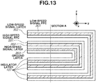
- Fig. 13 is a sectional view of Fig. 12 taken along the yz plane, seen in the x-axis direction. A layer structure will be described with reference to Fig. 13 .
- the low-speed signal FPC 301 is a single layer FPC including one conductor layer.
- a low-speed signal layer 302 refers to a conductor layer that includes only low-speed signal lines different from the electrical signal lines having the highest speed among those of the electrical signals to be transmitted by the FPC 104.
- the high-speed signal FPC 201 is a two-layer FPC including two conductor layers.
- the conductor layers of the high-speed signal FPC 201 are configured in such a manner that a high-speed signal layer 202 is on the outer side of the U shape and a ground layer 203 is on the inner side.
- the high-speed signal layer 202 refers to a conductor layer that includes the electrical signal lines having the highest speed among those of the electrical signals to be transmitted by the FPC 104. Other signal lines and power supply lines may be laid alongside.
- the ground layer 203 is a wiring layer including a ground line. The ground layer 203 provides ground wiring so as to overlap the high-speed signal lines.
- the high-speed signal layer 202 lying in the center of the U shape is shielded from both sides by the ground layer 203 and the low-speed signal layer 302.
- EMI electromagnetic interference
- the insulator layers 107 are layers for electrically separating the conductor layers.
- the insulator layers 107 are made of an insulator such as polyimide.
- the low-speed signal layer 302, the high-speed signal layer 202, and the ground layer 203 are thereby electrically separated.
- An adhesive is used to physically connect the insulator, such as polyimide, with the conductors. A description of the adhesive will be omitted since the adhesive is included in insulators (in the case of a conductive adhesive, conductors).
- High-flex rolled copper foil can be used as the conductors of the conductor layers for enhanced bending durability. Electrolytic copper foil, special electrolytic copper foil, or rolled copper foil may be used for portions that is subjected to less bending or sliding.
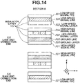
- Fig. 14 is a sectional view of Fig. 12 taken along the xz plane, seen in the y-axis direction (section A of Fig. 13 ).
- a wiring structure of the FPC 104 will be described with reference to Fig. 14 .
- High-speed signal lines 204 such as a video signal line are laid in the high-speed signal layer 202.
- a ground line 205 like a mesh ground is laid over the entire ground layer 203.
- a low-speed signal line 303 such a driving signal line of an autofocus (AF) motor for AF driving is laid in the low-speed signal layer 302.
- AF autofocus
- the ground layer 203 provides ground wiring overlapped to cover the inner side of the high-speed signal lines 204 of the high-speed signal layer 202 in the z-axis direction.
- the low-speed signal layer 302 similarly provides wiring overlapped to cover the outer side of the high-speed signal lines 204 in the z-axis direction. In such a manner, the high-speed signal lines 204 can be efficiently shielded.
- ground line 205 desirably covers the entire surface of the ground layer 203 to provide a wide shielding surface. However, the ground line 205 may be laid only in areas overlapping the high-speed signal lines 204. If the ground line 205 is laid only in areas overlapping the high-speed signal lines 204 in the ground layer 203, low-speed signal lines different from the ground line 205 may be laid in the remaining space in the ground layer 203.
- the ground line 205 may have gaps like meshes and slits.
- the ground line 205 may be a gapless one like a solid ground. If the ground layer 203 includes gaps as described above, the conductor volume decreases to soften the FPC 104. As a result, durability thereof is improved.
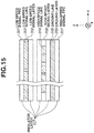
- Fig. 15 illustrates a configuration in which the high-speed signal lines 204 are covered with a plurality of low-speed signal lines 303.
- a low-speed signal line 303 is desirably laid by using a line thick enough to cover the high-speed signal lines 204.
- a plurality of low-speed signal lines 303 may be laid, not just one. If a plurality of low-speed signal lines 303 is used for shielding, the smaller the line-to-line interval, the higher the shielding characteristic.
- Driving signal lines severe tens of kilohertz band
- the low-speed signal lines 303 are equivalent to a direct-current (DC) potential, which enables EMI shielding.
- the low-speed signal FPC 301 itself has the function of suppressing noise of the high-speed signal FPC 201. As a result, noise can thus be suppressed without the addition of a dedicated noise suppression member to the high-speed signal lines 204.
- the communication speed of the high-speed signal lines 204 will be described.
- a lens unit 102 and a main unit 103 communicate a large amount of video data at 500 Mbps.
- Other transmission signals including high-frequency integrated circuit (IC) clock (CLK) and synchronization signals, have frequencies of not higher than 100 MHz.
- the video signal can be said to have the highest frequency.
- the high-speed signal lines 204 are not limited to video signals. For example, if the IC CLK has the highest frequency, the IC CLK is transmitted by a high-speed signal line 204. Note that the numerical values are merely examples and not restrictive.
- Fig. 16 is a detailed wiring structure diagram of the high-speed signal FPC 201.
- the video signal is transmitted by a transmission method such as low voltage differential signaling (LVDS), using at least a differential pair of lines.
- LVDS low voltage differential signaling
- Such a method often performs parallel transmission, in which case a plurality (ten pairs or so) of high-speed signal lines 204 is used.
- the high-speed signals of such a differential configuration suppress signal reflection to improve transmission path characteristics and EMI characteristics through matching of characteristic impedances of the transmission lines.
- Zdiff 2 * Z 0 * 1 ⁇ 0.48 * exp ⁇ 0.96 * S / H
- Z 0 60 / 0.475 ⁇ ⁇ r + 0.67 ⁇ ln 4 ⁇ H / 0.67 ⁇ 0.8 ⁇ W + T
- S is the interval between strip lines
- W is the width of the signal lines
- the metal thickness T will be described.
- the metal thickness T of a signal line can be appropriately selected from among 9 ⁇ m, 12 ⁇ m, 18 ⁇ m, and 35 ⁇ m, which are the thicknesses of typical materials.
- Concerning the metal thickness T there is a tradeoff between a resistance component and hardness of the signal line. If the metal thickness T is increased to increase the sectional area W*T of the signal line, the resistance component decreases and signal quality improves. However, as the metal thickness T increases, the FPC itself becomes harder and the bendability deteriorates.
- the metal thickness T can be determined based on the needed signal quality and bendability.
- the distance H between the signal lines and the ground line 205 is a parameter for setting the characteristic impedance Zdiff to a desired value.
- Concerning the distance H there is a tradeoff between the signal quality and the EMI characteristic. Since the characteristic impedance Zdiff decreases as the metal thickness T increases, the distance H between the signal lines and the ground line 205 needs to be increased accordingly so that the characteristic impedance Zdiff has a desired value.
- the distance H typically is 6 ⁇ m to 35 ⁇ m. If the distance H is increased, the coupling capacitance between the signal lines and the ground layer 203 decreases and the pass characteristic of high frequency components improves.
- the EMI characteristic deteriorates as the coupling capacitance between the signal lines and the ground line 205 decreases.
- the distance H between the signal lines and the ground line 205 can be determined in consideration of the needed signal quality and EMI characteristic.
- the width W and the interval S of the signal lines will be described.
- the width W of a signal line is a parameter for setting the characteristic impedance Zdiff to a desired value.
- Concerning the width W there is a tradeoff between the signal quality and layout (FPC width). From formulas (1) and (2), the width W is calculated so as to provide a desired characteristic impedance Zdiff. Since the width W affects the sectional area W * T of the signal line, the resistance component of the signal line can be reduced by increasing the width W. The greater the width W, the greater the FPC width. The width W can thus be determined in consideration of the signal quality and layout.
- the interval S between the strip lines is a parameter for setting the characteristic impedance Zdiff to a desired value.
- the interval S is calculated to provide a desired characteristic impedance Zdiff.
- layout needs to be taken into consideration. Since the interval S between the signal lines of a differential signal also affects the signal quality and EMI characteristic, attention is needed not to make the interval S extremely small or large.
- the parameters (T, H, W, and S) can be determined to meet the constraints on the EMI characteristic, signal quality characteristic, bending characteristic, and layout of the imaging apparatus.
- a through hole (TH) 110 is formed between the high-speed signal layer (surface conductor layer) 202 and the ground layer (backside conductor layer) 203 to connect conductors of the high-speed signal layer 202 and the ground layer 203. This can make the ground of the high-speed signal layer 202 and the ground layer 203 the same in potential.
- TH 110 is described to be used for ground connection
- an opening may be made in the surface insulator layer to expose the conductor layer if the high-speed signal FPC 201 has no TH 110.
- the exposed conductor layer then can be connected to metal of ground potential.
- the forming method of the ground layer 203 is not limited to that of a two-sided FPC including an overlap of two single layer FPCs. Instead, a conductive sheet or conductive film generated by silver deposition or copper rolling may be attached to a single layer FPC. In such a case, the ground wiring portion of the single layer FPC is exposed, and the exposed ground wiring and the conductor portion of the conductive sheet is desirably connected by a conductive adhesive.
- Fig. 17 is a connection diagram of the high-speed signal FPC 201.
- a method for connecting the high-speed signal layer 202 to each unit will be described with reference to Fig. 17.
- Fig. 17 illustrates an imaging apparatus 101 in which the high-speed signal FPC 201 is connected to the lens unit 102 (which refers to a unit similar to the lens unit 61 of Fig. 1 ) and the main unit 103 (which refers to a unit similar to the electric substrate 44 of Fig. 1 ).
- the connection terminals connectors 109 conforming to the high-speed signal FPC 201 are installed on the electric substrates of the respective units.
- Processing for removing insulation portions of the high-speed signal FPC 201 is performed so that the high-speed signal layer 202 makes contact with metal contacts 108 of the connectors 109. It is preferable to perform plating on the conductor portions to prevent oxidation. If connectors are not installable, the electric substrates and the high-speed signal FPC 201 may be connected by screwing or soldering.
- connection method is not limited to connectors. Screwing or soldering may be employed.
- FIG. 6 is an exploded view of a pan tilt camera according to the present embodiment.
- An electric substrate 14 and a motor unit 15 are attached to a bottom case 12.
- An inner case 13 is integrally attached to the bottom case 12.
- the bottom case 12, the inner case 13, the electric substrate 14, and the motor unit 15 constitute a non-rotating unit.
- a pan rotation table 21 is fitted to a protruding portion (not illustrated) at the center of the bottom case 12, and attached to the bottom case 12 by a stop ring 26 to be rotatable in a pan direction.
- a pan rotation table 21 includes a helical gear. The pan rotation table 21 is driven to rotate in the pan direction by driving a worm gear of a motor unit 15.
- An FPC 24 for controlling a lens unit 31 and an FPC 23 for transmitting an imaging signal from the lens unit 31 are attached to the inner case 13.
- Fig. 7 illustrates a developed configuration diagram of the FPCs 23 and 24 according to the present embodiment.
- Fig. 8 illustrates a detailed assembly diagram of the FPCs 23 and 24 according to the present embodiment.
- Terminal portions 23a and 24a of the FPCs 23 and 24 are connector-connected and fixed to the electric substrate 14.
- the FPCs 23 and 24 include arc-shaped first portions 23b and 24b, which are coaxial with a pan rotation axis.
- the arc-shaped first portions 23b and 24b are arranged on a surface perpendicular to the pan rotation axis.
- the inner case 13 includes a hook portion 13a for fixing the FPCs 23 and 24 so that the FPCs 23 and 24 will not lift in the direction of the pan rotation axis during a pan rotation.
- the inner case 13 further includes a protrusion 13b for guiding the arc-shaped first portions 23b and 24b so as to prevent the arc-shaped first portions 23b and 24b from shifting in a direction perpendicular to the pan rotation axis.
- the protrusion 13b is arranged substantially around the entire circumference except where the FPCs 23 and 24 are fixed to the electric substrate 14. With this configuration, the arc-shaped first portions 23b and 24b can be constantly maintained coaxial with the pan rotation axis.
- the pan rotation table 21 includes a protruding portion 21a, which is pressed and fitted into fixing holes 23c and 24c of the FPCs 23 and 24.
- the FPCs 23 and 24 are fixed in such a manner that the arc-shaped first portions 23b and 24b are bent around an axis orthogonal to the pan rotation axis.
- Fig. 9 is a diagram illustrating the bending of the FPCs 23 and 24 according to the present embodiment.
- the FPC 23 is arranged on the upper side of the inner case 13 with the FPC 24 therebetween.
- the FPC 23 is arranged inside the FPC 24.
- the arc-shaped first portions 23b and 24b need to be bent around respective different axes orthogonal to the pan rotation axis so that the bending position of the FPC 23 always lies in front of that of the FPC 24. If the bending position of the FPC 23 coincides with or comes behind that of the FPC 24, the bending positions fail to slide over the arc shape due to the occurrence of interference.
- Figs. 10A to 10C are shape change diagrams of the FPCs 23 and 24 during a pan rotation according to the present embodiment.
- Fig. 10A illustrates the shape of the FPCs 23 and 24 when the pan rotation table 21 is panned to the maximum counterclockwise. The bending positions of the first portions 23b and 24b come closest to the protruding portion 21a of the pan rotation table 21.
- Fig. 10B illustrates the shape of the FPCs 23 and 24 in an intermediate position of pan rotation. The bending positions slide over the arc shape by the amount of movement always one half that of the pan rotation.
- Fig. 10C illustrates the shape of the FPCs 23 and 24 when the pan rotation table 21 is panned to the maximum clockwise.
- An inner cover 22 is integrally attached to the pan rotation table 21.
- the inner cover 22 includes a groove 22a for guiding the folding portions when the arc-shaped first portions 23b and 24b of the FPCs 23 and 24 are bent.
- the inner cover 22 further includes a retaining shape 22b for preventing the FPCs 23 and 24 fixed to the inner case 13 from lifting.
- the retaining shape 22b is formed in an area where the folding portions will not reach when the arc-shaped first portions 23b and 24b are bent.
- the inner cover 22 further includes a hole 22c.
- the protruding portion 21a of the pan rotation table 21, running through the fixing holes 23c and 24c of the FPCs 23 and 24, is fitted to the hole 22c, whereby the FPCs 23 and 24 are prevented from coming off from the protruding portion 21a.
- Figs. 11A and 11B are shape change diagrams of the FPCs 23 and 24 during a tilt rotation according to the present embodiment.
- Fig. 11A illustrates the shape of the FPCs 23 and 24 when the lens optical axis of the lens unit 31 is horizontally directed.
- Fig. 11B illustrates the shape of the FPCs 23 and 24 when the lens optical axis of the lens unit 31 is vertically directed.
- the bending positions slide over the straight portion 23d by the amount of movement always one half that of the tilt rotation.
- the bending positions of the straight portion 23d and the U-shaped portion 24d are shifted in the planar direction and thus do not interfere with each other.
- the tilt rotation only produces a change of the FPCs 23 and 24, in which the bending positions slide, without a change in route or orientation of portions other than the outwardly-shaped portions. Stress on the FPCs 23 and 24 from a tilt rotation is thus limited to the range of the bending positions and to simple bending only. This improves durability.
- a hole is formed in the inner cover 22 so that the lens unit 31, the front cover 33, and the tilt rotation case 32 do not interfere during a tilt rotation.
- a transparent hemispherical dome cover is integrally attached to a top cover 11 to enable imaging regardless of pan and tilt orientations of the lens unit 31.
- the top cover 11 is fixed to the bottom case 12.
- the rotation of the rotating unit only produces a change of the FPCs 23 and 24, in which the bending positions simply slide over the arc-shaped first portions 23b and 24b. Since the portions other than the arc-shaped first portions 23b and 24b do not change in route or orientation, durability improves. Since the arc-shaped first portions 23b and 24b are bent only once, the configuration can be made small in the height direction. As seen in a plane of projection in the pan rotation axis direction, the moving range of the FPCs 23 and 24 is limited to the arc-shaped first portions 23b and 24b and their extended circle. Therefore, the configuration can also be made small in the direction of the outer diameter about the pan rotation axis.
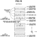
- Fig. 19 illustrates a sectional view of an overlap of two FPCs similar to those of Fig. 14 (section A of Fig. 13 ) in a thickness direction of the FPCs.
- a structure for reducing a distance dhl between the high-speed signal FPC 201 and a low-speed signal FPC 301 illustrated in Fig. 19 to improve shielding characteristics will be described.
- the bending radius of an FPC is determined by the hardness of the FPC. The harder the FPC, the larger the bending radius.
- the bending radius of the high-speed signal FPC 201 can be increased.
- the high-speed signal FPC 201 can be brought close to the low-speed signal FPC 301 for improved shielding characteristics.
- the high- and low-speed signal FPCs 201 and 301 may desirably be brought so close that the surface insulators make contact with each other.
- the reduced distance can cause crosstalk, depending on signal waveforms.
- a method for hardening the high-speed signal FPC 201 will be described.
- a major factor of the hardness of an FPC is the thickness of its conductor layer(s). If the low-speed signal FPC 301 has a conductor thickness of 35 ⁇ m, the conductor thickness of the high-speed signal FPC 201 is set to be thicker than or equal to 35 ⁇ m. Since the high-speed signal FPC 201 has a two-layer structure, such a conductor thickness can be achieved by forming each layer with a conductor thickness of 18 ⁇ m.
- the hardness also varies depending on the wiring area and material of the conductors, and the thickness and material of the insulators.
- the structure of the high- and low-speed signal FPCs 201 and 301 may be desirably determined in consideration of such factors.
- Figs. 20A and 20B are sectional views taken along the section A of Fig. 13 according to the first embodiment.
- Fig. 20A illustrates a case in which the high-speed signal FPC 201 is hard.
- Fig. 20B illustrates a case in which the low-speed signal FPC 301 is hard.
- the total thickness of all the conductor layers is the same.
- the high-speed signal FPC 201 has a large bending radius rha. Therefore, the low-speed signal FPC 301 overlapped on the outer side has a large bending radius rla.
- Fig. 20B a case in which the two FPCs 201 and 301 are reversed in hardness, i.e., the outer low-speed signal FPC 301 is hard and the inner high-speed signal FPC 201 is soft will be described.
- the high-speed signal FPC 201 has a bending radius rhb smaller than the bending radius rha in Fig. 20A .
- the bending radius rlb of the low-speed signal FPC 301 is determined by the hardness of the low-speed signal FPC 301 regardless of the bending radius rhb of the high-speed signal FPC 201. Therefore, bending radius rha of the high-speed signal FPC 201 in Fig. 20A coincides with the bending radius rlb of the low-speed signal FPC 301 in Fig. 20B .
- a comparison between the sizes of the folding portions in Figs. 20A and 20B shows that if the total thickness of the high- and low-speed signal FPCs 201 and 301 is the same, the folded FPCs 201 and 301 in Fig. 20A are greater by the thickness Hla of the low-speed signal FPC 301. In other words, making the outer low-speed signal FPC 301 harder than the inner high-speed signal FPC 201 enables miniaturization thereof.
- a single layer FPC has a thickness of approximately 0.03 to 0.12 mm. Since the U shape provides upper and lower, two strokes of reduction, an improvement of approximately 0.06 to 0.24 mm in diameter can be expected.
- the conductor thickness of the high-speed signal FPC 201 is set to be smaller than 35 ⁇ m. Since the high-speed signal FPC 201 has a two-layer structure, such a conductor thickness can be achieved by forming each layer with a conductor thickness of 12 ⁇ m, i.e., the two layers with a conductor thickness of 24 ⁇ m.
- Fig. 21 is a sectional view illustrating a layer structure when the ground layer 203 of the high-speed signal FPC 201, which is the two-layer FPC, is separated. As illustrated in Fig. 21 , all the FPCs are configured as single layer FPCs.
- a ground FPC 206 which is an example of a ground FPC, and the high- and low-speed signal FPCs 201 and 301 are arranged in this order from the innermost side of the U shape.
- Such a structure can reduce the thickness per FPC to enhance the bending durability of the FPCs.
- EMI shielding can be robust. For example, by making the innermost ground FPC 206 the hardest, and the outermost low-speed signal FPC 301 the softest, the overlapping portions of the FPCs can be brought into contact with each other. This not only provides robust EMI shielding, but also can stabilize the distances between the conductor layers for stable impedance and improved waveform quality.
- Fig. 22 illustrates an overall structure of an FPC 104 according to a sixth embodiment of the present invention.
- the x-axis direction is a width direction of the FPC 104
- the y-axis direction is a length direction of the FPC 104
- the z-axis direction is a thickness (height) direction of the FPC 104.
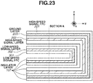
- Fig. 23 is a sectional view of Fig. 22 taken along the yz plane, seen in the x-axis direction. The layer configuration will be described with reference to Fig. 23 .
- the low-speed signal FPC 301 is a single layer FPC including one conductor layer.
- the low-speed signal layer 302 refers to a conductor layer including only low-speed signal lines without electrical signal lines having the highest speed among those of electrical signals to be transmitted by the FPC 104.
- the high-speed signal FPC 201 is a two-layer FPC including two conductor layers.
- Fig. 24 is a sectional view of Fig. 22 (section A of Fig. 23 ) taken along the xz plane, seen in the y-axis direction.
- a wiring structure of the FPC 104 will be described with reference to Fig. 24 .
- High-speed signal lines 204 such as a video signal line are laid in the high-speed signal layer 202.
- a ground line 205 such as a mesh ground is laid over the entire ground layer 203.
- a low-speed signal line 303 such as a driving signal line of an AF motor for AF driving is laid in the low-speed signal layer 302.
- the ground layer 203 provides ground wiring overlapped to cover the outer side of the high-speed signal lines 204 of the high-speed signal layer 202 on the z-axis.
- the low-speed signal layer 302 provides wiring overlapped to cover the inner side of the high-speed signal lines 204 on the z-axis. In such a manner, the high-speed signal lines 204 can be efficiently shielded.
- Driving signal lines severe tens of kilohertz band
- the low-speed signal lines 303 are equivalent to a direct-current (DC) potential, which enables EMI shielding.
- the low-speed signal FPC 301 itself has the function of suppressing noise of the high-speed signal FPC 201. Therefore, noise can be suppressed without the addition of a dedicated noise suppression member to the high-speed signal lines 204.
- a structure for reducing a distance dhl between the low-speed signal FPC 301 and the high-speed signal FPC 201 illustrated in Fig. 26 to improve shielding characteristics will be described.
- the bending radius of an FPC is determined by the hardness of the FPC. The harder the FPC, the larger the bending radius.
- the bending radius of the low-speed signal FPC 301 can be increased. With such a structure, the low-speed signal FPC 301 can be brought close to the high-speed signal FPC 201 for improved shielding characteristics.
- the high- and low-speed signal FPCs 201 and 301 may desirably be brought close to each other so that the surface insulators make contact with each other.
- the reduced distance can cause crosstalk, depending on signal waveforms.
- the signal waveforms may desirably be made less sharp to eliminate overshoots and undershoots for crosstalk suppression.
- a method for hardening the low-speed signal FPC 301 will be described.
- a major factor of the hardness of an FPC is the thickness of the conductor layer(s). If the low-speed signal FPC 301 has a conductor thickness of 35 ⁇ m, the conductor thickness of the high-speed signal FPC 201 is set to be smaller than or equal to 35 ⁇ m. Since the high-speed signal FPC 201 has a two-layer structure, such a conductor thickness can be achieved by forming each layer with a conductor thickness of 12 ⁇ m.
- the hardness also varies depending on the wiring area and material of the conductors, and the thickness and material of the insulators.
- the structure of the high- and low-speed signal FPCs 201 and 301 may desirably be determined in consideration of such factors.
- the eighth embodiment deals with a method for reducing the apparatus size by making the high-speed signal FPC 201 of the FPC 104 according to the sixth embodiment harder than the low-speed signal FPC 301.
- Figs. 27A and 27B are sectional views of Fig. 23 according to the sixth embodiment, taken along the section A.
- Fig. 27A illustrates a case in which the low-speed signal FPC 301 is hard.
- Fig. 27B illustrates a case in which the high-speed signal FPC 201 is hard.
- the total thickness of all the conductor layers is the same.
- the low-speed signal FPC 301 has a large bending radius rla. Therefore, the high-speed signal FPC 201 overlapped on the outer side has a large bending radius rha.
- Fig. 27B a case in which the two FPCs 201 and 301 are reversed in hardness, i.e., the outer high-speed signal FPC 201 is hard and the inner low-speed signal FPC 301 is soft will be described.
- the low-speed signal FPC 301 has a bending radius rlb smaller than the bending radius rla in Fig. 27A .
- the bending radius rhb of the high-speed signal FPC 201 is determined by the hardness of the high-speed signal FPC 201 regardless of the bending radius rlb of the low-speed signal FPC 301. Therefore, bending radius rla of the low-speed signal FPC 301 in Fig. 27A coincides with the bending radius rhb of the high-speed signal FPC 201 in Fig. 27B .
- FIG. 27A and 27B shows that if the high- and low-speed signal FPCs 201 and 301 have the same total thickness, the folded FPCs 201 and 301 in Fig. 27A are greater by the thickness Hha of the high-speed signal FPC 201. In other words, making the outer high-speed signal FPC 201 harder than the inner low-speed signal FPC 301 enables miniaturization thereof.
- a two-layer FPC has a thickness of approximately 0.04 to 0.30 mm. Since the U shape provides upper and lower, i.e., two strokes of reduction, an improvement of approximately 0.08 to 0.60 mm in diameter can thus be expected.
- the conductor thickness of the high-speed signal FPC 201 is set to be greater than 35 ⁇ m. Since the high-speed signal FPC 201 has a two-layer structure, such a conductor thickness can be achieved by forming each layer with a conductor thickness of 18 ⁇ m, i.e., the two layers with a conductor thickness of 36 ⁇ m.
- the hardness also varies depending on the wiring area and material of the conductors, and the thickness and material of the insulators.
- the structure of the high- and low-speed signal FPCs 201 and 301 may desirably be determined in consideration of such factors.
- the high-speed signal FPC 201 may be hardened relative to the low-speed signal FPC 301.
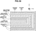
- Fig. 28 is a sectional view illustrating a layer configuration in which the ground layer 203 of the high-speed signal FPC 201, which is the two-layer FPC, is separated. As illustrated in Fig. 28 , all the FPCs are configured as single layer FPCs.
- the low-speed signal FPC 301, the high-speed signal FPC 201, and a ground FPC 206 are arranged in this order from the innermost side of the U shape. Such a structure can reduce the thickness per FPC to enhance the bending durability of the FPCs.
- EMI shielding can be robust. For example, by making the innermost low-speed signal FPC 301 the hardest and the outermost ground FPC 206 the softest, the overlapping portions of the FPCs can be brought into contact with each other. This not only provides robust EMI shielding, but also can stabilize the distances between the conductor layers for stable impedance and improved waveform quality.
- Fig. 29 is a sectional view of Fig. 12 taken along the yz plane, seen in the x-axis direction. The layer structure will be described with reference to Fig. 29 .
- the low-speed signal FPC 301 is a single layer FPC including one conductor layer.
- the low-speed signal layer 302 refers to a conductor layer that includes only low-speed signal lines without including the electrical signal lines having the highest speed among those of the electrical signals to be transmitted by the FPC 104.
- the high-speed signal FPC 201 is a two-layer FPC including two conductor layers.
- the conductor layers of the high-speed signal FPC 201 are configured in such a manner that a high-speed signal layer 202 is on the inner side of the U shape and a ground layer 203 is on the outer side.
- the high-speed signal layer 202 refers to a conductor layer that includes the electrical signal lines having the highest speed among those of the electrical signals to be transmitted by the FPC 104. Other signal lines and power supply lines may be laid side by side.
- the ground layer 203 is a wiring layer including a ground line. The ground layer 203 provides ground wiring so as to overlap the high-speed signal lines.
- the high-speed signal layer 202 on the innermost side of the U shape is doubly shielded by the ground layer 203 and the low-speed signal layer 302. Therefore, EMI characteristics are improved.
- the provision of the ground layer 203 between the low-speed signal layer 302 and the high-speed signal layer 202 can prevent crosstalk between the low-speed signal lines and the high-speed signal lines.
- Fig. 30 is a sectional view of Fig. 12 (section A of Fig. 29 ) taken along the xz plane, seen in the y-axis direction.
- a wiring structure of the FPC 104 will be described with reference to Fig. 30 .
- High-speed signal lines 204 such as a video signal line are laid in the high-speed signal layer 202.
- a ground line 205 like a mesh ground is laid over the entire ground layer 203.
- a low-speed signal line 303 such a driving signal line of an AF motor for AF driving is laid in the low-speed signal layer 302.
- the ground layer 203 provides ground wiring overlapped to cover the high-speed signal lines 204 of the high-speed signal layer 202 on the z-axis.
- the low-speed signal layer 302 similarly provides wiring overlapped to cover the high-speed signal lines 204 on the z-axis. In such a manner, the high-speed signal lines 204 can be efficiently shielded.
- Driving signal lines severe tens of kilohertz band
- the low-speed signal lines 303 are equivalent to a direct-current (DC) potential, which enables EMI shielding.
- the low-speed signal FPC 301 itself has the function of suppressing noise of the high-speed signal FPC 201. Therefore, noise can be suppressed without the addition of a dedicated noise suppression member to the high-speed signal lines 204.
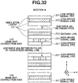
- a structure for reducing a distance dhl between the high-speed signal FPC 201 and the low-speed signal FPC 301 illustrated in Fig. 32 to improve shielding characteristics will be described.
- the bending radius of an FPC is determined by the hardness of the FPC. The harder the FPC, the larger the bending radius.
- the high-speed signal FPC 201 harder than the low-speed signal FPC 301, the bending radius of the high-speed signal FPC 201 can be increased. With such a structure, the high-speed signal FPC 201 can be brought close to the low-speed signal FPC 301 for improved shielding characteristics.
- High-speed signal FPC 201 may be hardened relative to the low-speed signal FPC 301.
- the embodiments of the imaging apparatus according to the present invention have been described above.
- the arc-shaped first and second portions are bent around axes orthogonal to the axes in the pan and tilt rotation directions, respectively.
- the embodiments can be similarly applied to any combinations of rotation directions including a roll rotation direction.
Landscapes
- Engineering & Computer Science (AREA)
- Physics & Mathematics (AREA)
- General Physics & Mathematics (AREA)
- Multimedia (AREA)
- Signal Processing (AREA)
- Optics & Photonics (AREA)
- Microelectronics & Electronic Packaging (AREA)
- General Engineering & Computer Science (AREA)
- Mechanical Engineering (AREA)
- Studio Devices (AREA)
- Structure Of Printed Boards (AREA)
- Accessories Of Cameras (AREA)
Abstract
Description
- The present invention relates to a wiring structure of a monitoring camera apparatus operable in pan and tilt directions.
- Among monitoring camera apparatuses to be installed on the ceiling and wall surfaces is a pan tilt camera, in which a lens unit can be operated in pan, tilt, and roll directions to monitor a plurality of places. A pan tilt camera includes a lens unit including an image sensor, and a fixed unit including an electric substrate. An imaging signal from the image sensor is transmitted from the lens unit to the electric substrate via a cable or a flexible printed circuit. The cable or flexible printed circuit needs to be configured to follow changes in route resulting from rotational movements of the lens unit in the pan, tilt, and roll directions.
- As a conventional example in which a flexible printed circuit is used for a camera, Japanese Patent Application Laid-Open No.
2015-220938 2015-220938 - A pan tilt camera needs two axes for pan and tilt. If, for example, the configuration discussed in Japanese Patent Application Laid-Open No.
2015-220938 - The present invention is directed to an imaging apparatus including a flexible printed circuit that can follow changes in route resulting from rotational movements without complication.
- According to an aspect of the present invention, there is provided an imaging apparatus as specified in claims 1 to 27.
- Further features of the present invention will become apparent from the following description of embodiments with reference to the attached drawings.
-
-
Fig. 1 is an exploded view of a pan tilt camera according to a first embodiment. -
Fig. 2 is a developed configuration diagram of flexible printed circuits according to the first embodiment. -
Fig. 3 is a detailed assembly diagram of the flexible printed circuits according to the first embodiment. -
Fig. 4 is a diagram illustrating bending of the flexible printed circuits according to the first embodiment. -
Figs. 5A and 5B are shape change diagrams of the flexible printed circuits according to the first embodiment. -
Fig. 6 is an exploded view of a pan tilt camera according to a second embodiment. -
Fig. 7 is a developed configuration diagram of flexible printed circuits according to the second embodiment. -
Fig. 8 is a detailed assembly diagram of the flexible printed circuits according to the second embodiment. -
Fig. 9 is a diagram illustrating bending of the flexible printed circuits according to the second embodiment. -
Figs. 10A, 10B, and 10C are shape change diagrams of the flexible printed circuits during a tilt rotation according to the second embodiment. -
Figs. 11A and 11B are shape change diagrams of the flexible printed circuits during a tilt rotation according to the second embodiment. -
Fig. 12 is a structure diagram of the flexible printed circuits (FPCs) according to the first embodiment. -
Fig. 13 is a layer configuration diagram of the FPCs according to the first embodiment. -
Fig. 14 is a wiring structure diagram of the FPCs according to the first embodiment. -
Fig. 15 is a wiring structure diagram illustrating multi-line wiring of the FPCs according to the first embodiment. -
Fig. 16 is a detailed wiring structure diagram of a high-speed signal FPC according to the first embodiment. -
Fig. 17 is a diagram illustrating a method for connecting the high-speed signal FPC according to the first embodiment. -
Fig. 18 is a diagram illustrating a method for connecting a low-speed signal FPC according to the first embodiment. -
Fig. 19 is a diagram illustrating a distance between FPCs according to a third embodiment. -
Figs. 20A and 20B are diagrams illustrating miniaturization of FPCs according to a fourth embodiment. -
Fig. 21 is a diagram illustrating a three-part divided structure of FPCs according to a fifth embodiment. -
Fig. 22 is a U-shape structure diagram of FPCs according to a sixth embodiment. -
Fig. 23 is a layer configuration diagram of the FPCs according to the sixth embodiment. -
Fig. 24 is a wiring structure diagram of the FPCs according to the sixth embodiment. -
Fig. 25 is a wiring structure diagram illustrating multi-line wiring of the FPCs according to the sixth embodiment. -
Fig. 26 is a diagram illustrating a distance between FPCs according to a seventh embodiment. -
Figs. 27A and 27B are diagrams illustrating miniaturization of FPCs according to an eighth embodiment. -
Fig. 28 is a diagram illustrating a three-part divided structure of FPCs according to a ninth embodiment. -
Fig. 29 is a layer configuration diagram of FPCs according to a tenth embodiment. -
Fig. 30 is a wiring structure diagram of the FPCs according to the tenth embodiment. -
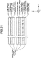
Fig. 31 is a wiring structure diagram illustrating multi-line wiring of the FPCs according to the tenth embodiment. -
Fig. 32 is a diagram illustrating a distance between FPCs according to an eleventh embodiment. -
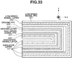
Fig. 33 is a diagram illustrating a three-part divided structure of FPCs according to a twelfth embodiment. - First, a first embodiment of the present invention will be described.
Fig. 1 is an exploded view of a pan tilt camera according to the present embodiment. Anelectric substrate 44 and amotor unit 45 are attached to abottom case 42. Aninner case 43 is integrally attached to thebottom case 42. Thebottom case 42, theinner case 43, theelectric substrate 44, and themotor unit 45 constitute a non-rotating unit. - A pan rotation table 51 serving as a rotation unit is fitted to a protruding portion (not illustrated) at the center of the
bottom case 42, and attached to thebottom case 42 by astop ring 56 to be rotatable in a pan direction. The pan rotation table 51 includes a helical gear. By driving a worm gear of themotor unit 45, the pan rotation table 51 can rotate in the pan direction. Flexible printedcircuits inner case 43. The flexible printedcircuit 53 is an example of a first flexible printed circuit for controlling alens unit 61. The flexible printedcircuit 54 is an example of a second flexible printed circuit for transmitting an imaging signal from thelens unit 61. -
Fig. 2 is a developed configuration diagram of the flexible printedcircuits Fig. 3 is a detailed assembly diagram of the flexible printedcircuits Terminal portions circuits electric substrate 44. The flexible printedcircuits first portions first portions first portions inner case 43 includes ahook portion 43a for fixingportions circuits inner case 43 further includes a protrudingportion 43b for guiding the arc-shapedfirst portions first portions portion 43b is arranged substantially around the entire circumference except where the flexible printedcircuits electric substrate 44. With this configuration, arc-shapedfirst portions - The pan rotation table 51 includes a protruding
portion 51a which is pressed and fitted into fixingholes circuits circuits first portions portions 51b and a fold-back guide portion 51c. The protrudingportions 51b guide the flexible printedcircuits - The flexible printed
circuit 53 is arranged on the upper side of theinner case 43 with the flexible printedcircuit 54 therebetween. Therefore, when the arc-shapedfirst portions circuit 53 is arranged inside the flexible printedcircuit 54. The arc-shapedfirst portions circuit 53 always lies in front of that of the flexible printedcircuit 54. If the plurality of flexible printedcircuits first portion 53b to be shorter than the first portion 45b. Alternatively, if the flexible printedcircuits circuits hook portion 43a of theinner case 43 and the protrudingportion 51a of the pan rotation table 51 need to be provided for each of the flexible printedcircuits - An
inner cover 52 is integrally attached to the pan rotation table 51. Theinner cover 52 includes agroove shape 52a for guiding the folding portions when the arc-shapedfirst portions circuits inner cover 52 further includes a retainingportion 52b for preventing the flexible printedcircuits inner case 43 from lifting. The retainingportion 52b is arranged in an area where the folding portions will not reach when the arc-shapedfirst portions inner cover 52 includes ahole 52c. The protrudingportion 51a of the pan rotation table 51, running through the fixingholes circuits hole 52c, to prevent the flexible printedcircuits portion 51a. - The
inner cover 52 and theinner case 43 are configured to cover the arc-shapedfirst portions circuits inner cover 52 and theinner case 43 with resin having an electromagnetic shielding property, noise of the flexible printedcircuits side cover 63 and atilt gear case 62 are attached to alens unit 61. Thetilt gear case 62 includes arotation shaft 62a which is fitted to and supported by a bearingportion 51d arranged on the pan rotation table 51. Thetilt gear case 62 includes a helical gear. By driving a worm gear of amotor unit 55 fixed to the pan rotation table 51, thetilt gear case 62 can be driven to rotate in a tilt direction. - The flexible printed
circuits first portions hook portion 63a for fixing the flexible printedcircuits circuits portion 63b for guiding the arc-shapedfirst portions first portions first portions - As illustrated in
Fig. 4 , alens substrate 64, animaging substrate 65, and alens plate 66 are attached to thelens unit 61. Thelens substrate 64 controls thelens unit 61. An image sensor is mounted on theimaging substrate 65. Thelens plate 66 supports theimaging substrate 65. - As illustrated in
Figs. 2 and4 , the flexible printedcircuit 53 includes another arc-shapedsecond portion 53d inside the arc-shapedfirst portion 53b. The arc-shapedsecond portion 53d of the flexible printedcircuit 53 is bent perpendicularly to the tilt rotation axis. A fixingportion 53g of the flexible printedcircuit 53 is fixed to thehook portion 63a of theside cover 63. Aterminal portion 53e of the flexible printedcircuit 53 is fixed and connected to theimaging substrate 65. - The flexible printed
circuit 54 includes another arc-shapedsecond portion 54d inside the arc-shapedfirst portion 54b. The arc-shapedsecond portion 54d of the flexible printedcircuit 54 is bent perpendicularly to the tilt rotation axis. A fixingportion 54g of the flexible printedcircuit 54 is fixed to thehook portion 63a of theside cover 63. Aterminal portion 54e of the flexible printedcircuit 54 is fixed and connected to thelens substrate 64. - As illustrated in
Fig. 2 , the flexible printedcircuits straight portions straight portions straight portions first portions second portions straight portions second portions Fig. 4 , the firststraight portions lens unit 61. As illustrated inFig. 4 , the secondstraight portions -
Figs. 5A and 5B are shape change diagrams of the flexible printedcircuits Fig. 5A illustrates the shape of the flexible printedcircuits lens unit 61 is horizontally directed.Fig. 5B illustrates the shape of the flexible printedcircuits lens unit 61 is vertically directed. The bending positions slide over the arc shape by the amount of movement always one half that of the tilt rotation. - A hole is formed in the
inner cover 52 so that thelens unit 61, theside cover 63, and thetilt gear case 62 do not interfere during a tilt rotation. A transparent hemispherical dome cover is integrally attached to atop cover 41 to enable imaging regardless of pan and tilt orientations of thelens unit 61. Thetop cover 41 is fixed to thebottom case 42. - With the foregoing configuration, the rotation of the rotating unit only produces a change of the flexible printed
circuits first portions first portions first portions circuits first portions - An embodiment of an imaging apparatus of the present invention has been described above. In the present embodiment, the imaging apparatus is configured in such a manner that the arc-shaped
first portions second portions - Next, details of the flexible printed
circuits - The flexible printed
circuit 53 is an example of a high-speed signal flexible printed circuit, and includes high-speed signal lines, which are electrical signal lines having the highest speed among those of electrical signals to be transmitted by the flexible printedcircuits circuit 53 will hereinafter be referred to as a high-speed signal flexible printed circuit (FPC) 201. TheFPC 54 is an example of a low-speed signal FPC, and includes only low-speed signal lines different from the electrical signal lines having the highest speed. TheFPC 54 will hereinafter be referred to as a low-speed signal FPC 301. Thus, thelow signal FPC 301 transmits low-speed signals different from high-speed signals. -
Fig. 12 illustrates an overall structure of the high- and low-speed signal FPCs Fig. 12 , the x-axis direction is a width direction of the high- and low-speed signal FPCs speed signal FPCs speed signal FPCs - The high- and low-
speed signal FPCs speed signal FPCs speed signal FPCs Fig. 12 , and the foldedFPCs speed signal FPC 301 is arranged to cover the high-speed signal FPC 201. Such a U-shaped structure enables the low-speed signal FPC 301 to absorb radio waves radiated from the high-speed signal FPC 201 inside. This can reduce radiated waves and enable shielding without mechanical members. - The high- and low-
speed signal FPCs FPC 104 of divided structure. Such a divided structure significantly reduces the FPC width. For example, suppose that an FPC width of approximately 20 mm is needed to juxtapose all lines including signal lines, control signal lines, and power supply lines in a single layer FPC. Suppose also that the single layer FPC has a thickness of approximately 0.05 mm. If the FPC is divided into two and overlapped, the thickness doubles or increases by approximately 0.05 mm while the FPC width decreases to one half or by 10 mm. Although there is a gap between the FPCs and the foregoing does not apply completely, such a slight increase in thickness can reduce the width significantly. It should be noted that the numerical values are merely examples and not restrictive. - Longitudinal ends of the
FPC 104 serve as connection terminals for respective units. The longitudinal ends will be referred to as a lensunit connection end 105 and a mainunit connection end 106. -
Fig. 13 is a sectional view ofFig. 12 taken along the yz plane, seen in the x-axis direction. A layer structure will be described with reference toFig. 13 . The low-speed signal FPC 301 is a single layer FPC including one conductor layer. InFig. 12 , a low-speed signal layer 302 refers to a conductor layer that includes only low-speed signal lines different from the electrical signal lines having the highest speed among those of the electrical signals to be transmitted by theFPC 104. The high-speed signal FPC 201 is a two-layer FPC including two conductor layers. The conductor layers of the high-speed signal FPC 201 are configured in such a manner that a high-speed signal layer 202 is on the outer side of the U shape and aground layer 203 is on the inner side. The high-speed signal layer 202 refers to a conductor layer that includes the electrical signal lines having the highest speed among those of the electrical signals to be transmitted by theFPC 104. Other signal lines and power supply lines may be laid alongside. Theground layer 203 is a wiring layer including a ground line. Theground layer 203 provides ground wiring so as to overlap the high-speed signal lines. - With such a structure, the high-
speed signal layer 202 lying in the center of the U shape is shielded from both sides by theground layer 203 and the low-speed signal layer 302. As a result, electromagnetic interference (EMI) characteristics are improved. - Next, insulator layers 107 will be described. The insulator layers 107 are layers for electrically separating the conductor layers. The insulator layers 107 are made of an insulator such as polyimide. The low-
speed signal layer 302, the high-speed signal layer 202, and theground layer 203 are thereby electrically separated. An adhesive is used to physically connect the insulator, such as polyimide, with the conductors. A description of the adhesive will be omitted since the adhesive is included in insulators (in the case of a conductive adhesive, conductors). High-flex rolled copper foil can be used as the conductors of the conductor layers for enhanced bending durability. Electrolytic copper foil, special electrolytic copper foil, or rolled copper foil may be used for portions that is subjected to less bending or sliding. -
Fig. 14 is a sectional view ofFig. 12 taken along the xz plane, seen in the y-axis direction (section A ofFig. 13 ). A wiring structure of theFPC 104 will be described with reference toFig. 14 . First, the wiring structure of each conductor layer will be described. High-speed signal lines 204 such as a video signal line are laid in the high-speed signal layer 202. Aground line 205 like a mesh ground is laid over theentire ground layer 203. A low-speed signal line 303 such a driving signal line of an autofocus (AF) motor for AF driving is laid in the low-speed signal layer 302. - The overlapping of the wiring of the layers will be described. The
ground layer 203 provides ground wiring overlapped to cover the inner side of the high-speed signal lines 204 of the high-speed signal layer 202 in the z-axis direction. The low-speed signal layer 302 similarly provides wiring overlapped to cover the outer side of the high-speed signal lines 204 in the z-axis direction. In such a manner, the high-speed signal lines 204 can be efficiently shielded. - There may be a plurality of high-
speed signal lines 204, not just one. All the high-speed signal lines 204 desirably are laid next to each other and covered with theground line 205 and the low-speed signal line 303. In view of EMI shielding, theground line 205 desirably covers the entire surface of theground layer 203 to provide a wide shielding surface. However, theground line 205 may be laid only in areas overlapping the high-speed signal lines 204. If theground line 205 is laid only in areas overlapping the high-speed signal lines 204 in theground layer 203, low-speed signal lines different from theground line 205 may be laid in the remaining space in theground layer 203. Theground line 205 may have gaps like meshes and slits. Theground line 205 may be a gapless one like a solid ground. If theground layer 203 includes gaps as described above, the conductor volume decreases to soften theFPC 104. As a result, durability thereof is improved. -
Fig. 15 illustrates a configuration in which the high-speed signal lines 204 are covered with a plurality of low-speed signal lines 303. In view of EMI shielding, a low-speed signal line 303 is desirably laid by using a line thick enough to cover the high-speed signal lines 204. A plurality of low-speed signal lines 303 may be laid, not just one. If a plurality of low-speed signal lines 303 is used for shielding, the smaller the line-to-line interval, the higher the shielding characteristic. - The principle and effect of shielding the high-
speed signal lines 204 by the low-speed signal lines 303 will be described. Driving signal lines (several tens of kilohertz band) of an AF motor, having a sufficiently low frequency with respect to that of the high-speed signal lines 204 (several hundreds of megahertz band), are used as the low-speed signal lines 303. With this configuration, as seen from the high-speed signal lines 204, the low-speed signal lines 303 are equivalent to a direct-current (DC) potential, which enables EMI shielding. In other words, the low-speed signal FPC 301 itself has the function of suppressing noise of the high-speed signal FPC 201. As a result, noise can thus be suppressed without the addition of a dedicated noise suppression member to the high-speed signal lines 204. - The communication speed of the high-
speed signal lines 204 will be described. Alens unit 102 and amain unit 103 communicate a large amount of video data at 500 Mbps. Other transmission signals, including high-frequency integrated circuit (IC) clock (CLK) and synchronization signals, have frequencies of not higher than 100 MHz. The video signal can be said to have the highest frequency. However, the high-speed signal lines 204 are not limited to video signals. For example, if the IC CLK has the highest frequency, the IC CLK is transmitted by a high-speed signal line 204. Note that the numerical values are merely examples and not restrictive. - The wiring of the high-
speed signal lines 204 will be described.Fig. 16 is a detailed wiring structure diagram of the high-speed signal FPC 201. The video signal is transmitted by a transmission method such as low voltage differential signaling (LVDS), using at least a differential pair of lines. Such a method often performs parallel transmission, in which case a plurality (ten pairs or so) of high-speed signal lines 204 is used. The high-speed signals of such a differential configuration suppress signal reflection to improve transmission path characteristics and EMI characteristics through matching of characteristic impedances of the transmission lines. Combined with theground layer 203, the high-speed signal lines 204 form coplanar lines, of which a differential characteristic impedance (Zdiff) can be derived by formulas (1) and (2) :

ground line 205, and εr is the dielectric constant of the dielectric. - Methods for determining the parameters (T, H, W, and S) and tradeoffs will be described by using an example. First, the metal thickness T will be described. The metal thickness T of a signal line can be appropriately selected from among 9 µm, 12 µm, 18 µm, and 35 µm, which are the thicknesses of typical materials. Concerning the metal thickness T, there is a tradeoff between a resistance component and hardness of the signal line. If the metal thickness T is increased to increase the sectional area W*T of the signal line, the resistance component decreases and signal quality improves. However, as the metal thickness T increases, the FPC itself becomes harder and the bendability deteriorates. The metal thickness T can be determined based on the needed signal quality and bendability.
- Next, the distance H between the signal lines and the
ground line 205 will be described. The distance H between the signal lines and theground line 205 is a parameter for setting the characteristic impedance Zdiff to a desired value. Concerning the distance H, there is a tradeoff between the signal quality and the EMI characteristic. Since the characteristic impedance Zdiff decreases as the metal thickness T increases, the distance H between the signal lines and theground line 205 needs to be increased accordingly so that the characteristic impedance Zdiff has a desired value. The distance H typically is 6 µm to 35 µm. If the distance H is increased, the coupling capacitance between the signal lines and theground layer 203 decreases and the pass characteristic of high frequency components improves. However, the EMI characteristic deteriorates as the coupling capacitance between the signal lines and theground line 205 decreases. To achieve a desired characteristic impedance Zdiff, the distance H between the signal lines and theground line 205 can be determined in consideration of the needed signal quality and EMI characteristic. - The width W and the interval S of the signal lines will be described. The width W of a signal line is a parameter for setting the characteristic impedance Zdiff to a desired value. Concerning the width W, there is a tradeoff between the signal quality and layout (FPC width). From formulas (1) and (2), the width W is calculated so as to provide a desired characteristic impedance Zdiff. Since the width W affects the sectional area W * T of the signal line, the resistance component of the signal line can be reduced by increasing the width W. The greater the width W, the greater the FPC width. The width W can thus be determined in consideration of the signal quality and layout. The interval S between the strip lines is a parameter for setting the characteristic impedance Zdiff to a desired value. From the formulas (1) and (2), the interval S is calculated to provide a desired characteristic impedance Zdiff. The greater the interval S, the greater the FPC width. Thus, layout needs to be taken into consideration. Since the interval S between the signal lines of a differential signal also affects the signal quality and EMI characteristic, attention is needed not to make the interval S extremely small or large. In such a manner, the parameters (T, H, W, and S) can be determined to meet the constraints on the EMI characteristic, signal quality characteristic, bending characteristic, and layout of the imaging apparatus.
- Next, a method for connecting the
ground layer 203 will be described. If a two-layer FPC is used, a through hole (TH) 110 is formed between the high-speed signal layer (surface conductor layer) 202 and the ground layer (backside conductor layer) 203 to connect conductors of the high-speed signal layer 202 and theground layer 203. This can make the ground of the high-speed signal layer 202 and theground layer 203 the same in potential. - While the
TH 110 is described to be used for ground connection, an opening may be made in the surface insulator layer to expose the conductor layer if the high-speed signal FPC 201 has noTH 110. The exposed conductor layer then can be connected to metal of ground potential. The forming method of theground layer 203 is not limited to that of a two-sided FPC including an overlap of two single layer FPCs. Instead, a conductive sheet or conductive film generated by silver deposition or copper rolling may be attached to a single layer FPC. In such a case, the ground wiring portion of the single layer FPC is exposed, and the exposed ground wiring and the conductor portion of the conductive sheet is desirably connected by a conductive adhesive. -
Fig. 17 is a connection diagram of the high-speed signal FPC 201. A method for connecting the high-speed signal layer 202 to each unit will be described with reference toFig. 17. Fig. 17 illustrates an imaging apparatus 101 in which the high-speed signal FPC 201 is connected to the lens unit 102 (which refers to a unit similar to thelens unit 61 ofFig. 1 ) and the main unit 103 (which refers to a unit similar to theelectric substrate 44 ofFig. 1 ). For the connection terminals,connectors 109 conforming to the high-speed signal FPC 201 are installed on the electric substrates of the respective units. Processing for removing insulation portions of the high-speed signal FPC 201 is performed so that the high-speed signal layer 202 makes contact withmetal contacts 108 of theconnectors 109. It is preferable to perform plating on the conductor portions to prevent oxidation. If connectors are not installable, the electric substrates and the high-speed signal FPC 201 may be connected by screwing or soldering. -
Fig. 18 is a connection diagram of the low-speed signal FPC 301. A method for connecting the low-speed signal lines 303 to each unit will be described with reference toFig. 18 . In the imaging apparatus 101 ofFig. 18 , like the high-speed signal FPC 201, the low-speed signal FPC 301 is connected to thelens unit 102 and themain unit 103 viametal contacts 108 ofconnectors 109. - The connection method is not limited to connectors. Screwing or soldering may be employed.
- The low-
speed signal lines 303 are not limited to the driving signal lines of an AF motor, and may include any line of frequency lower than that of the high-speed signal lines 204. Examples include lines of a synchronization signal, a control signal, and a power supply voltage, driving signal lines different from those of an AF motor, and analog lines of a thermistor. - While the low-
speed signal FPC 301 is described to be one in number, there may be a plurality of low-speed signal FPCs 301. In such a case, the low-speed signal lines may be desirably arranged on the outer side of the U shape. - Next, a second embodiment of the present invention will be described.
Fig. 6 is an exploded view of a pan tilt camera according to the present embodiment. Anelectric substrate 14 and amotor unit 15 are attached to abottom case 12. Aninner case 13 is integrally attached to thebottom case 12. Thebottom case 12, theinner case 13, theelectric substrate 14, and themotor unit 15 constitute a non-rotating unit. - A pan rotation table 21 is fitted to a protruding portion (not illustrated) at the center of the
bottom case 12, and attached to thebottom case 12 by astop ring 26 to be rotatable in a pan direction. A pan rotation table 21 includes a helical gear. The pan rotation table 21 is driven to rotate in the pan direction by driving a worm gear of amotor unit 15. AnFPC 24 for controlling alens unit 31 and anFPC 23 for transmitting an imaging signal from thelens unit 31 are attached to theinner case 13. -
Fig. 7 illustrates a developed configuration diagram of theFPCs Fig. 8 illustrates a detailed assembly diagram of theFPCs Terminal portions FPCs electric substrate 14. TheFPCs first portions first portions - The
inner case 13 includes ahook portion 13a for fixing theFPCs FPCs inner case 13 further includes aprotrusion 13b for guiding the arc-shapedfirst portions first portions protrusion 13b is arranged substantially around the entire circumference except where theFPCs electric substrate 14. With this configuration, the arc-shapedfirst portions - The pan rotation table 21 includes a protruding
portion 21a, which is pressed and fitted into fixingholes FPCs FPCs first portions -
Fig. 9 is a diagram illustrating the bending of theFPCs FPC 23 is arranged on the upper side of theinner case 13 with theFPC 24 therebetween. Thus, when the arc-shapedfirst portions FPC 23 is arranged inside theFPC 24. The arc-shapedfirst portions FPC 23 always lies in front of that of theFPC 24. If the bending position of theFPC 23 coincides with or comes behind that of theFPC 24, the bending positions fail to slide over the arc shape due to the occurrence of interference. - If a plurality of FPCs is configured to be overlapped in such a manner, the bending axes perpendicular to the pan rotation axis can be made different by configuring the arc-shaped
first portion 23b to be shorter than the arc-shapedfirst portion 24b. Alternatively, if theFPCs FPCs hook portion 13a of theinner case 13 and the protrudingportion 21a of the pan rotation table 21 need to be provided for each of theFPCs - In the present embodiment described above, the imaging apparatus includes two
FPCs lens unit 31 does not need to be controlled, the imaging apparatus may include only theFPC 23 for transmitting the imaging signal. -
Figs. 10A to 10C are shape change diagrams of theFPCs Fig. 10A illustrates the shape of theFPCs first portions portion 21a of the pan rotation table 21.Fig. 10B illustrates the shape of theFPCs Fig. 10C illustrates the shape of theFPCs FPCs portion 21a of the pan rotation table 21 pass over the ends of the arc-shapedfirst portions hook portion 13a of theinner case 13 and move onto the extended circle of the arc-shapedfirst portions - An
inner cover 22 is integrally attached to the pan rotation table 21. Theinner cover 22 includes agroove 22a for guiding the folding portions when the arc-shapedfirst portions FPCs inner cover 22 further includes a retainingshape 22b for preventing theFPCs inner case 13 from lifting. The retainingshape 22b is formed in an area where the folding portions will not reach when the arc-shapedfirst portions inner cover 22 further includes ahole 22c. The protrudingportion 21a of the pan rotation table 21, running through the fixingholes FPCs hole 22c, whereby theFPCs portion 21a. - The
inner cover 22 and theinner case 13 are configured to cover the arc-shapedfirst portions FPCs FPCs inner cover 22 and theinner case 13 with resin having an electromagnetic shielding property. - A
front cover 33 and atilt rotation case 32 are attached to thelens unit 31. Thetilt rotation case 32 includes atilt rotation shaft 32a, which is fitted to and supported by a bearingportion 21b arranged on the pan rotation table 21. Thetilt rotation case 32 includes a helical gear. By driving a worm gear of amotor unit 25 fixed to the pan rotation table 21, thetilt rotation case 32 can be driven to rotate in a tilt direction. As illustrated inFig. 9 , alens substrate 34, animaging substrate 35, and alens plate 36 are attached to thelens unit 31. Thelens substrate 34 controls thelens unit 31. An image sensor is mounted on theimaging substrate 35. Thelens plate 36 supports thelens substrate 34 and theimaging substrate 35. - As illustrated in
Fig. 7 , theFPC 23 includes astraight portion 23d extending inward from the end of the arc-shapedfirst portion 23b. Thestraight portion 23d of theFPC 23 is bent in parallel with the tilt rotation axis, and aterminal portion 23e is fixed and connected to thelens substrate 34. TheFPC 24 includes aU-shaped portion 24d which extends inward from the end of the arc-shapedfirst portion 24b, makes a U-turn, and extends outward. The outward straight shape of theU-shaped portion 24d of theFPC 24 is bent in parallel with the tilt rotation axis, and aterminal portion 24e is fixed and connected to theimaging substrate 35. -
Figs. 11A and 11B are shape change diagrams of theFPCs Fig. 11A illustrates the shape of theFPCs lens unit 31 is horizontally directed.Fig. 11B illustrates the shape of theFPCs lens unit 31 is vertically directed. The bending positions slide over thestraight portion 23d by the amount of movement always one half that of the tilt rotation. The bending positions of thestraight portion 23d and theU-shaped portion 24d are shifted in the planar direction and thus do not interfere with each other. Since thestraight portion 23d and theU-shaped portion 24d are bent in parallel with the tilt rotation axis, the tilt rotation only produces a change of theFPCs FPCs - A hole is formed in the
inner cover 22 so that thelens unit 31, thefront cover 33, and thetilt rotation case 32 do not interfere during a tilt rotation. A transparent hemispherical dome cover is integrally attached to atop cover 11 to enable imaging regardless of pan and tilt orientations of thelens unit 31. Thetop cover 11 is fixed to thebottom case 12. - With the foregoing configuration, the rotation of the rotating unit only produces a change of the
FPCs first portions first portions first portions FPCs first portions - Next, a third embodiment of the present invention will be described below. The third embodiment deals with a case in which the high-
speed signal FPC 201 of theFPC 104 according to the first embodiment is hardened.Fig. 19 illustrates a sectional view of an overlap of two FPCs similar to those ofFig. 14 (section A ofFig. 13 ) in a thickness direction of the FPCs. - A structure for reducing a distance dhl between the high-
speed signal FPC 201 and a low-speed signal FPC 301 illustrated inFig. 19 to improve shielding characteristics will be described. The bending radius of an FPC is determined by the hardness of the FPC. The harder the FPC, the larger the bending radius. By making high-speed signal FPC 201 harder than the low-speed signal FPC 301, the bending radius of the high-speed signal FPC 201 can be increased. By such a structure, the high-speed signal FPC 201 can be brought close to the low-speed signal FPC 301 for improved shielding characteristics. In view of EMI, the high- and low-speed signal FPCs - A method for hardening the high-
speed signal FPC 201 will be described. A major factor of the hardness of an FPC is the thickness of its conductor layer(s). If the low-speed signal FPC 301 has a conductor thickness of 35 µm, the conductor thickness of the high-speed signal FPC 201 is set to be thicker than or equal to 35 µm. Since the high-speed signal FPC 201 has a two-layer structure, such a conductor thickness can be achieved by forming each layer with a conductor thickness of 18 µm. - The hardness also varies depending on the wiring area and material of the conductors, and the thickness and material of the insulators. The structure of the high- and low-
speed signal FPCs - Making the high-
speed signal FPC 201 harder than the low-speed signal FPC 301 improves EMI characteristics. The greater the difference in hardness, the higher the effect. It is useful to harden the high-speed signal FPC 201 relative to the low-speed signal FPC 301. - Next, a fourth embodiment of the present invention will be described. A method for reducing the apparatus size by making the low-
speed signal FPC 301 of theFPC 104 according to the first embodiment harder than the high-speed signal FPC 201 will be described. - First, concerning a conductor thickness, a tradeoff between electric characteristics and an apparatus size will be described. In view of the electric characteristics, by increasing the conductor thickness, resistance components can be reduced. Greater conductor thickness is therefore desirable. However, in view of the apparatus size, harder FPCs causes larger bending radii. Smaller conductor thicknesses are therefore desirable. Whether to increase or decrease the conductor thickness is therefore not simply determinable. A structure that can miniaturize the structure of the
FPC 104 according to the first embodiment with the same total thickness of the conductor layers will be described. -
Figs. 20A and 20B are sectional views taken along the section A ofFig. 13 according to the first embodiment.Fig. 20A illustrates a case in which the high-speed signal FPC 201 is hard.Fig. 20B illustrates a case in which the low-speed signal FPC 301 is hard. InFigs. 20A and 20B , the total thickness of all the conductor layers is the same. - As illustrated in
Fig. 20A , if the inner high-speed signal FPC 201 is hard, the high-speed signal FPC 201 has a large bending radius rha. Therefore, the low-speed signal FPC 301 overlapped on the outer side has a large bending radius rla. Referring toFig. 20B , a case in which the twoFPCs speed signal FPC 301 is hard and the inner high-speed signal FPC 201 is soft will be described. The high-speed signal FPC 201 has a bending radius rhb smaller than the bending radius rha inFig. 20A . Since the low-speed signal FPC 301 harder than the high-speed signal FPC 201 is overlapped on the outer side, the bending radius rlb of the low-speed signal FPC 301 is determined by the hardness of the low-speed signal FPC 301 regardless of the bending radius rhb of the high-speed signal FPC 201. Therefore, bending radius rha of the high-speed signal FPC 201 inFig. 20A coincides with the bending radius rlb of the low-speed signal FPC 301 inFig. 20B . - A comparison between the sizes of the folding portions in
Figs. 20A and 20B shows that if the total thickness of the high- and low-speed signal FPCs FPCs Fig. 20A are greater by the thickness Hla of the low-speed signal FPC 301. In other words, making the outer low-speed signal FPC 301 harder than the inner high-speed signal FPC 201 enables miniaturization thereof. A single layer FPC has a thickness of approximately 0.03 to 0.12 mm. Since the U shape provides upper and lower, two strokes of reduction, an improvement of approximately 0.06 to 0.24 mm in diameter can be expected. - A specific design example will be described. If the low-
speed signal FPC 301 has a conductor thickness of 35 µm, the conductor thickness of the high-speed signal FPC 201 is set to be smaller than 35 µm. Since the high-speed signal FPC 201 has a two-layer structure, such a conductor thickness can be achieved by forming each layer with a conductor thickness of 12 µm, i.e., the two layers with a conductor thickness of 24 µm. - The hardness also varies depending the wiring area and material of the conductors, and the thickness and material of the insulators. It is useful to determine the structure of the high- and low-
speed signal FPCs - Making the low-
speed signal FPC 301 harder than the high-speed signal FPC 201 enables miniaturization thereof. It is useful to harden the low-speed signal FPC 301 relative to the high-speed signal FPC 201. - Next, a fifth embodiment of the present invention will be described. The fifth embodiment deals with a case in which the two-layer FPC according to the first embodiment is divided into two FPCs.
Fig. 21 is a sectional view illustrating a layer structure when theground layer 203 of the high-speed signal FPC 201, which is the two-layer FPC, is separated. As illustrated inFig. 21 , all the FPCs are configured as single layer FPCs. Aground FPC 206, which is an example of a ground FPC, and the high- and low-speed signal FPCs - By making the inner FPCs of the U shape hard, EMI shielding can be robust. For example, by making the
innermost ground FPC 206 the hardest, and the outermost low-speed signal FPC 301 the softest, the overlapping portions of the FPCs can be brought into contact with each other. This not only provides robust EMI shielding, but also can stabilize the distances between the conductor layers for stable impedance and improved waveform quality. -
Fig. 22 illustrates an overall structure of anFPC 104 according to a sixth embodiment of the present invention. InFig. 22 , the x-axis direction is a width direction of theFPC 104, the y-axis direction is a length direction of theFPC 104, and the z-axis direction is a thickness (height) direction of theFPC 104. - A high-
speed signal FPC 201 and a low-speed signal FPC 301 both have a folding structure. With the folding structure, the low-speed signal FPC 301 and the high-speed signal FPC 201 have a U shape. The high- and low-speed signal FPCs Fig. 22 , and the foldedFPCs speed signal FPC 301 is thus arranged to cover the inner side of the high-speed signal FPC 201. Such a U-shaped structure allows the low-speed signal FPC 301 to absorb radio waves radiated from the high-speed signal FPC 201 inside. -
Fig. 23 is a sectional view ofFig. 22 taken along the yz plane, seen in the x-axis direction. The layer configuration will be described with reference toFig. 23 . The low-speed signal FPC 301 is a single layer FPC including one conductor layer. InFig. 23 , the low-speed signal layer 302 refers to a conductor layer including only low-speed signal lines without electrical signal lines having the highest speed among those of electrical signals to be transmitted by theFPC 104. On the other hand, the high-speed signal FPC 201 is a two-layer FPC including two conductor layers. The conductor layers of the high-speed signal FPC 201 are configured in such a manner that a high-speed signal layer 202 is on the inner side of the U shape, and aground layer 203 is on the outer side. The high-speed signal layer 202 refers to a conductor layer including the electrical signal lines having the highest speed among those of the electrical signals to be transmitted by theFPC 104. Other signal lines and power supply lines may be laid side by side. Theground layer 203 is a wiring layer including a ground line. Theground layer 203 provides ground wiring so as to overlap high-speed signal lines. With such a structure, the high-speed signal layer 202 lying in the center of the U shape is shielded from both sides by theground layer 203 and the low-speed signal layer 302. In this way, EMI characteristics are improved. This can reduce radiated waves and enable shielding without mechanical members. -
Fig. 24 is a sectional view ofFig. 22 (section A ofFig. 23 ) taken along the xz plane, seen in the y-axis direction. A wiring structure of theFPC 104 will be described with reference toFig. 24 . First, the wiring structure of each conductor layer will be described. High-speed signal lines 204 such as a video signal line are laid in the high-speed signal layer 202. Aground line 205 such as a mesh ground is laid over theentire ground layer 203. A low-speed signal line 303 such as a driving signal line of an AF motor for AF driving is laid in the low-speed signal layer 302. - The overlapping of the wiring of the layers will be described. The
ground layer 203 provides ground wiring overlapped to cover the outer side of the high-speed signal lines 204 of the high-speed signal layer 202 on the z-axis. Similarly, the low-speed signal layer 302 provides wiring overlapped to cover the inner side of the high-speed signal lines 204 on the z-axis. In such a manner, the high-speed signal lines 204 can be efficiently shielded. - There may be a plurality of high-
speed signal lines 204, not just one. All the high-speed signal lines 204 may desirably be laid next to each other and covered with theground line 205 and the low-speed signal line 303. In view of EMI shielding, the entire surface of theground layer 203 may desirably be covered with theground line 205 to provide a wide shielding area. Theground line 205 may be laid only in areas overlapping the high-speed signal lines 204. If theground line 205 is laid only in areas overlapping the high-speed signal lines 204 in theground layer 203, low-speed signal lines other than theground line 205 may be laid in the remaining space in theground layer 203. Theground line 205 may have gaps like meshes and slits. Theground line 205 may be a gapless one like a solid ground. If theground layer 203 includes gaps as described above, the conductor volume decreases to soften theFPC 104 for improved durability. -
Fig. 25 illustrates a configuration in which the high-speed signal lines 204 are covered with a plurality of low-speed signal lines 303. In view of EMI shielding, a low-speed signal line 303 may desirably be laid by using a line having thickness enough to cover the high-speed signal lines 204. At that time a plurality of low-speed signal lines 303 may be laid, not just one. If a plurality of low-speed signal lines 303 is used for shielding, the shorter the line-to-line distance, the higher the shielding characteristic. - The principle and effect of shielding the high-
speed signal lines 204 by the low-speed signal lines 303 will be described. Driving signal lines (several tens of kilohertz band) of an AF motor, having a sufficiently low frequency with respect to that of the high-speed signal lines 204 (several hundreds of megahertz band), are used as the low-speed signal lines 303. As seen from the high-speed signal lines 204, the low-speed signal lines 303 are equivalent to a direct-current (DC) potential, which enables EMI shielding. In other words, the low-speed signal FPC 301 itself has the function of suppressing noise of the high-speed signal FPC 201. Therefore, noise can be suppressed without the addition of a dedicated noise suppression member to the high-speed signal lines 204. - Next, a seventh embodiment of the present invention will be described. The seventh embodiment deals with a case in which the low-
speed signal FPC 301 of theFPC 104 according to the sixth embodiment is hardened.Fig. 26 illustrates a sectional view of an overlap of two FPCs similar to those ofFig. 24 (section A ofFig. 23 ) in a thickness direction of the FPCs. - A structure for reducing a distance dhl between the low-
speed signal FPC 301 and the high-speed signal FPC 201 illustrated inFig. 26 to improve shielding characteristics will be described. The bending radius of an FPC is determined by the hardness of the FPC. The harder the FPC, the larger the bending radius. By making the low-speed signal FPC 301 harder than the high-speed signal FPC 201, the bending radius of the low-speed signal FPC 301 can be increased. With such a structure, the low-speed signal FPC 301 can be brought close to the high-speed signal FPC 201 for improved shielding characteristics. In view of EMI, the high- and low-speed signal FPCs - A method for hardening the low-
speed signal FPC 301 will be described. A major factor of the hardness of an FPC is the thickness of the conductor layer(s). If the low-speed signal FPC 301 has a conductor thickness of 35 µm, the conductor thickness of the high-speed signal FPC 201 is set to be smaller than or equal to 35 µm. Since the high-speed signal FPC 201 has a two-layer structure, such a conductor thickness can be achieved by forming each layer with a conductor thickness of 12 µm. - The hardness also varies depending on the wiring area and material of the conductors, and the thickness and material of the insulators. The structure of the high- and low-
speed signal FPCs - Making the lower-
speed signal FPC 301 harder than the high-speed signal FPC 201 improves EMI characteristics. The greater the difference in hardness, the higher the effect. Therefore, it is useful to make the low-speed signal FPC 301 hard relative to the high-speed signal FPC 201. - Next, an eighth embodiment of the present invention will be described. The eighth embodiment deals with a method for reducing the apparatus size by making the high-
speed signal FPC 201 of theFPC 104 according to the sixth embodiment harder than the low-speed signal FPC 301. - First, concerning a conductor thickness, a tradeoff between electric characteristics and an apparatus size will be described. In view of the electric characteristics, by increasing the conductor thickness, resistance components can be reduced. Greater conductor thicknesses are therefore desirable. However, in view of the apparatus size, harder FPCs have larger bending radii. Smaller conductor thicknesses are therefore desirable. Whether to increase or decrease the conductor thickness is therefore not simply determinable. A structure that can miniaturize the structure of the
FPC 104 according to the sixth embodiment with the same total thickness of the conductor layers will be described. -
Figs. 27A and 27B are sectional views ofFig. 23 according to the sixth embodiment, taken along the section A.Fig. 27A illustrates a case in which the low-speed signal FPC 301 is hard.Fig. 27B illustrates a case in which the high-speed signal FPC 201 is hard. InFigs. 27A and 27B , the total thickness of all the conductor layers is the same. - As illustrated in
Fig. 27A , if the inner low-speed signal FPC 301 is hard, the low-speed signal FPC 301 has a large bending radius rla. Therefore, the high-speed signal FPC 201 overlapped on the outer side has a large bending radius rha. On the other hand, referring toFig. 27B , a case in which the twoFPCs speed signal FPC 201 is hard and the inner low-speed signal FPC 301 is soft will be described. The low-speed signal FPC 301 has a bending radius rlb smaller than the bending radius rla inFig. 27A . Since the high-speed signal FPC 201 harder than the low-speed signal FPC 301 is overlapped on the outside thereof, the bending radius rhb of the high-speed signal FPC 201 is determined by the hardness of the high-speed signal FPC 201 regardless of the bending radius rlb of the low-speed signal FPC 301. Therefore, bending radius rla of the low-speed signal FPC 301 inFig. 27A coincides with the bending radius rhb of the high-speed signal FPC 201 inFig. 27B . A comparison between the sizes of the folding portions inFigs. 27A and 27B shows that if the high- and low-speed signal FPCs FPCs Fig. 27A are greater by the thickness Hha of the high-speed signal FPC 201. In other words, making the outer high-speed signal FPC 201 harder than the inner low-speed signal FPC 301 enables miniaturization thereof. A two-layer FPC has a thickness of approximately 0.04 to 0.30 mm. Since the U shape provides upper and lower, i.e., two strokes of reduction, an improvement of approximately 0.08 to 0.60 mm in diameter can thus be expected. - A specific design example will be described. If the low-
speed signal FPC 301 has a conductor thickness of 35 µm, the conductor thickness of the high-speed signal FPC 201 is set to be greater than 35 µm. Since the high-speed signal FPC 201 has a two-layer structure, such a conductor thickness can be achieved by forming each layer with a conductor thickness of 18 µm, i.e., the two layers with a conductor thickness of 36 µm. - The hardness also varies depending on the wiring area and material of the conductors, and the thickness and material of the insulators. The structure of the high- and low-
speed signal FPCs - Making the high-
speed signal FPC 201 harder than the low-speed signal FPC 301 enables miniaturization thereof. To that end, the high-speed signal FPC 201 may be hardened relative to the low-speed signal FPC 301. - Next, a ninth embodiment of the present invention will be described. The ninth embodiment deals with a case in which the two-layer FPC according to the sixth embodiment is divided into two FPCs.
Fig. 28 is a sectional view illustrating a layer configuration in which theground layer 203 of the high-speed signal FPC 201, which is the two-layer FPC, is separated. As illustrated inFig. 28 , all the FPCs are configured as single layer FPCs. The low-speed signal FPC 301, the high-speed signal FPC 201, and aground FPC 206 are arranged in this order from the innermost side of the U shape. Such a structure can reduce the thickness per FPC to enhance the bending durability of the FPCs. - By making the inner FPCs of the U shape hard, EMI shielding can be robust. For example, by making the innermost low-
speed signal FPC 301 the hardest and theoutermost ground FPC 206 the softest, the overlapping portions of the FPCs can be brought into contact with each other. This not only provides robust EMI shielding, but also can stabilize the distances between the conductor layers for stable impedance and improved waveform quality. -
Fig. 29 is a sectional view ofFig. 12 taken along the yz plane, seen in the x-axis direction. The layer structure will be described with reference toFig. 29 . The low-speed signal FPC 301 is a single layer FPC including one conductor layer. InFig. 29 , the low-speed signal layer 302 refers to a conductor layer that includes only low-speed signal lines without including the electrical signal lines having the highest speed among those of the electrical signals to be transmitted by theFPC 104. The high-speed signal FPC 201 is a two-layer FPC including two conductor layers. The conductor layers of the high-speed signal FPC 201 are configured in such a manner that a high-speed signal layer 202 is on the inner side of the U shape and aground layer 203 is on the outer side. The high-speed signal layer 202 refers to a conductor layer that includes the electrical signal lines having the highest speed among those of the electrical signals to be transmitted by theFPC 104. Other signal lines and power supply lines may be laid side by side. Theground layer 203 is a wiring layer including a ground line. Theground layer 203 provides ground wiring so as to overlap the high-speed signal lines. - With such a structure, the high-
speed signal layer 202 on the innermost side of the U shape is doubly shielded by theground layer 203 and the low-speed signal layer 302. Therefore, EMI characteristics are improved. In addition, the provision of theground layer 203 between the low-speed signal layer 302 and the high-speed signal layer 202 can prevent crosstalk between the low-speed signal lines and the high-speed signal lines. -
Fig. 30 is a sectional view ofFig. 12 (section A ofFig. 29 ) taken along the xz plane, seen in the y-axis direction. A wiring structure of theFPC 104 will be described with reference toFig. 30 . First, the wiring structure of each conductor layer will be described. High-speed signal lines 204 such as a video signal line are laid in the high-speed signal layer 202. Aground line 205 like a mesh ground is laid over theentire ground layer 203. A low-speed signal line 303 such a driving signal line of an AF motor for AF driving is laid in the low-speed signal layer 302. - The overlapping of the wiring of the layers will be described. The
ground layer 203 provides ground wiring overlapped to cover the high-speed signal lines 204 of the high-speed signal layer 202 on the z-axis. The low-speed signal layer 302 similarly provides wiring overlapped to cover the high-speed signal lines 204 on the z-axis. In such a manner, the high-speed signal lines 204 can be efficiently shielded. - There may be a plurality of high-
speed signal lines 204, not just one. All the high-speed signal lines 204 may desirably be laid next to each other and covered with theground line 205 and the low-signal line 303. In view of EMI shielding, theground line 205 may desirably cover the entire surface of theground layer 203 to provide a wide shielding surface. Theground line 205 may be laid only in areas overlapping the high-speed signal lines 204. If theground line 205 is laid only in areas overlapping the high-speed signal lines 204 in theground layer 203, low-speed signal lines other than theground line 205 may be laid in the remaining space in theground layer 203. Theground line 205 may have gaps like meshes and slits. Theground line 205 may be a gapless one like a solid ground. If theground layer 203 includes gaps as described above, the conductor volume decreases to soften theFPC 104 for improved durability. -
Fig. 31 illustrates a configuration in which the high-speed signal lines 204 are covered with a plurality of low-speed signal lines 303. In view of EMI shielding, a low-speed signal line 303 may desirably be laid by using a line having thickness enough to cover the high-speed signal lines 204. At that time, a plurality of low-speed signal lines 303 may be laid, not just one. If a plurality of low-speed signal lines 303 is used for shielding, the shorter the line-to-line distance, the higher the shielding characteristic. - The principle and effect of shielding the high-
speed signal lines 204 by the low-speed signal lines 303 will be described. Driving signal lines (several tens of kilohertz band) of an AF motor, having a sufficiently low frequency with respect to that of the high-speed signal lines 204 (several hundreds of megahertz band), are used as the low-speed signal lines 303. As seen from the high-speed signal lines 204, the low-speed signal lines 303 are equivalent to a direct-current (DC) potential, which enables EMI shielding. In other words, the low-speed signal FPC 301 itself has the function of suppressing noise of the high-speed signal FPC 201. Therefore, noise can be suppressed without the addition of a dedicated noise suppression member to the high-speed signal lines 204. - Next, an eleventh embodiment of the present invention will be described. The eleventh embodiment deals with a case in which the high-
speed signal FPC 201 of theFPC 104 according to the sixth embodiment is hardened.Fig. 32 illustrates a sectional view of an overlap of two FPCs similar to those ofFig. 30 (section A ofFig. 29 ) in a thickness direction of the FPCs. - A structure for reducing a distance dhl between the high-
speed signal FPC 201 and the low-speed signal FPC 301 illustrated inFig. 32 to improve shielding characteristics will be described. The bending radius of an FPC is determined by the hardness of the FPC. The harder the FPC, the larger the bending radius. By making the high-speed signal FPC 201 harder than the low-speed signal FPC 301, the bending radius of the high-speed signal FPC 201 can be increased. With such a structure, the high-speed signal FPC 201 can be brought close to the low-speed signal FPC 301 for improved shielding characteristics. - A method for hardening the high-
speed signal FPC 201 will be described. A major factor of the hardness of an FPC is the thickness of the conductor layer(s). If the low-speed signal FPC 301 has a conductor thickness of 35 µm, the conductor thickness of the high-speed signal FPC 201 is set to be greater than or equal to 35 µm. Since the high-speed signal FPC 201 has a two-layer structure, such a conductor thickness can be achieved by forming each layer with a conductor thickness of 18 µm. - The hardness also varies depending on the wiring area and material of the conductors, and the thickness and material of the insulators. The structure of the high- and low-
speed signal FPCs - Making the high-
speed signal FPC 201 harder than the low-speed signal FPC 301 improves EMI characteristics. The greater the difference therebetween in hardness, the higher the effect. Therefore, high-speed signal FPC 201 may be hardened relative to the low-speed signal FPC 301. - Making the high-
speed signal FPC 201 hard can also reduce crosstalk between the high-speed signal lines 204. The folding structure such as illustrated inFig. 29 causes crosstalk since the high-speed signal lines 204 are opposed to each other. The distance between the high-speed signal lines 204 will be denoted by dhh. The distance dhh between the high-speed signal lines 204 is determined by the bending radius of the high-speed signal FPC 201. The harder the high-speed signal FPC 201, the larger the bending radius and the greater the distance dhh between the high-speed signal lines 204. By increasing the distance dhh between the high-speed signal lines 204, the coupling capacitance between the high-speed signal lines 204 and reduce crosstalk can be reduced. - Next, a twelfth embodiment of the present invention will be described. The twelfth embodiment deals with a case in which the two-layer PFC according to the sixth embodiment is divided into two FPCs.
Fig. 33 is a sectional view illustrating a layer structure when theground layer 203 of the high-speed signal FPC 201, which is the two-layer FPC, is separated. As illustrated inFig. 33 , all of the FPCs are configured as single layer FPCs. The high-speed signal FPC 201, aground FPC 206, and the low-speed signal FPC 301 are arranged in this order from the innermost side of the U shape. Such a structure can reduce the thickness per FPC to enhance the bending durability of the FPCs. - Hardening the inner FPCs of the U shape enables EMI shielding robust. For example, by making the innermost high-
speed signal FPC 201 hardest and the outermost low-speed signal FPC 301 softest, the overlapping portions of the FPCs can be brought into contact with each other. This not only provides robust EMI shielding, but also can stabilize the distances between the conductor layers. As a result, stable impedance and thus improved waveform quality can be obtained. - The embodiments of the imaging apparatus according to the present invention have been described above. In the embodiments, the arc-shaped first and second portions are bent around axes orthogonal to the axes in the pan and tilt rotation directions, respectively. However, the embodiments can be similarly applied to any combinations of rotation directions including a roll rotation direction.
- While the present invention has been described with reference to embodiments, it is to be understood that the invention is not limited to the disclosed embodiments. The scope of the following claims is to be accorded the broadest interpretation so as to encompass all such modifications and equivalent structures and functions.
Claims (27)
- An imaging apparatus comprising:a lens means (61) including an image sensor, wherein the lens means can be tilted about a tilt rotation axis;a rotating means (51) configured to be rotatable about a pan rotation axis;a non-rotating means (42, 43, 44, 45) to which the rotating means is rotatably attached; anda flexible printed circuit (53, 54) configured to connect the lens means with the non-rotating means,wherein the flexible printed circuit includes an arc-shaped first portion (53b, 54b) coaxial with the pan rotation axis in a plane perpendicular to the pan rotation axis, and an arc-shaped second portion (53d, 54d) coaxial with the tilt rotation axis in a plane perpendicular to the tilt rotation axis, andwherein the first portion is bent around an axis orthogonal to the pan rotation axis.
- The imaging apparatus according to claim 1, wherein the rotating means (51) and the non-rotating means (42, 43, 44, 45) include a protruding portion (51a) or a hook portion (43a) configured to fix the first portion (53a, 54a) of the flexible printed circuit (53, 54).
- The imaging apparatus according to claim 2, wherein the first portion (53a, 54a) of the flexible printed circuit (53, 54) includes a hole (53c, 54c) which the protruding portion (51a) extends through.
- The imaging apparatus according to any preceding claim, wherein the lens means (61) includes a hook portion (63a) configured to fix the second portion (53d, 54d) of the flexible printed circuit (53, 54).
- The imaging apparatus according to any preceding claim, wherein the rotating means (51) and the non-rotating means (43) include a groove (52a) or a protrusion (43b) configured to guide the first portion (53b, 54b).
- The imaging apparatus according to any preceding claim,
wherein the flexible printed circuit (53, 54) includes a first straight portion (53h, 54h) configured to connect the first and second portions, and
wherein the first straight portion is bent around an axis parallel to an optical axis of the lens means (61). - The imaging apparatus according to any preceding claim,
wherein the flexible printed circuit (53, 54) includes a second straight portion (53i, 54i) extending from the second portion (53d, 54d), and
wherein the second straight portion is bent to be arranged in parallel with the tilt rotation axis. - The imaging apparatus according to any preceding claim, wherein the rotating means (51) and the non-rotation means (42, 43, 44, 45) are configured to cover the first portion (53b, 54b) of the flexible printed circuit (53, 54).
- The imaging apparatus according to any preceding claim, wherein at least one of the rotating means (51) and the non-rotating means (42, 43, 44, 45) is made of resin having an electromagnetic shielding property.
- The imaging apparatus according to any preceding claim,
wherein the flexible printed circuit includes a first flexible printed circuit (53) and a second flexible printed circuit (54), and
wherein the first and second flexible printed circuits are arranged in an overlapping manner. - The imaging apparatus according to claim 10, wherein the axis about which the first flexible printed circuit (53b) is bent is different from the axis about which the second flexible printed circuit (54b) is bent.
- The imaging apparatus according to claim 10 or 11, wherein the first portion (53b) of the first flexible printed circuit (53) and the first portion (54b) of the second flexible printed circuit (54) have different lengths.
- The imaging apparatus according to claim 11 or 12, wherein the first portion (53b) of the first flexible printed circuit (53) and the first portion (54b) of the second flexible printed circuit (54) have the same length, and are fixed to the rotating means and the non-rotating means at different positions.
- An imaging apparatus comprising:a lens means (61) including an image sensor;a rotating means (51) configured to be rotatable about a first axis;a non-rotating means (42, 43, 44, 45) to which the rotating means is rotatably attached; andat least a flexible printed circuit (53, 54, 23, 24) configured to connect the lens means with the non-rotating means, and including an arc portion (53b, 54b, 23b, 24b) coaxial with the first axis in a plane perpendicular to the first axis,wherein the arc portion is bent around a second axis orthogonal to the first axis, andwherein a plurality of the flexible printed circuits are arranged in an overlapping manner.
- The imaging apparatus according to claim 14, wherein the plurality of flexible printed circuits (53, 54, 23, 24) have different second axes.
- The imaging apparatus according to any one of claims 1 to 9,
wherein the flexible printed circuit includes
a high-speed signal flexible printed circuit (201) configured to transmit a high-speed signal having a highest frequency among signals to be transmitted by the flexible printed circuit, and
a low-speed signal flexible printed circuit (301) configured to transmit a low-speed signal different from the high-speed signal,
wherein the high-speed signal flexible printed circuit (201) includes a ground layer (203) and a high-speed signal layer (202). - The imaging apparatus according to claim 16,
wherein, when the flexible printed circuit is bent, the low-speed signal flexible printed circuit (301) is arranged on an outer side of the high-speed signal flexible printed circuit (201), and
wherein the high-speed signal flexible printed circuit (201) has the high-speed signal layer (202) outside and the ground layer (203) inside. - The imaging apparatus according to claim 16,
wherein, when the flexible printed circuit is bent, the low-speed signal flexible printed circuit (301) is arranged on an inner side of the high-speed signal flexible printed circuit (201), and
wherein the high-speed signal flexible printed circuit (201) has the high-speed signal layer (202) inside and the ground layer (203) outside. - The imaging apparatus according to claim 16,
wherein, when the flexible printed circuit is bent, the low-speed signal flexible printed circuit (301) is arranged on an outer side of the high-speed signal flexible printed circuit (201), and
wherein the high-speed signal flexible printed circuit (201) has the high-speed signal layer (202) inside and the ground layer (203) outside. - The imaging apparatus according to any one of claims 16 to 19, wherein the high-speed signal flexible printed circuit (201) is made harder than the low-speed signal flexible printed circuit (301).
- The imaging apparatus according to any one of claims 16 to 19, wherein the low-speed signal flexible printed circuit (301) is made harder than the high-speed signal flexible printed circuit (201).
- The imaging apparatus according to any one of claims 16 to 20, wherein wiring of the low-speed signal flexible printed circuit (301) is laid at a position overlapping with wiring of the high-speed signal flexible printed circuit (201).
- The imaging apparatus according to any one of claims 1 to 9,
wherein the flexible printed circuit includes
a high-speed signal flexible printed circuit (201) configured to transmit a high-speed signal having a highest frequency among signals to be transmitted by the flexible printed circuit,
a low-speed signal flexible printed circuit (301) configured to transmit a low-speed signal different from the high-speed signal, and
a ground flexible printed circuit (206) in which ground wiring is laid. - The imaging apparatus according to claim 23, wherein, when the flexible printed circuit is bent, the ground flexible printed circuit (206), the high-speed signal flexible printed circuit (201), and the low-speed signal flexible printed circuit (301) are arranged in this order from an innermost side.
- The imaging apparatus according to claim 23, wherein, when the flexible printed circuit is bent, the low-speed signal flexible printed circuit (301), the high-speed signal flexible printed circuit (201), and the ground flexible printed circuit (206) are arranged in this order from an innermost side.
- The imaging apparatus according to claim 23, wherein, when the flexible printed circuit is bent, the high-speed signal flexible printed circuit (201), the ground flexible printed circuit (206), and the low-speed signal flexible printed circuit (301) are arranged in this order from an innermost side.
- The imaging apparatus according to any one of claims 24 to 26, wherein a flexible printed circuit arranged on an inner side is made harder than a flexible printed circuit arranged on an outer side.
Applications Claiming Priority (2)
| Application Number | Priority Date | Filing Date | Title |
|---|---|---|---|
| JP2016211527 | 2016-10-28 | ||
| JP2017146340A JP6584458B2 (en) | 2016-10-28 | 2017-07-28 | Imaging device |
Publications (3)
| Publication Number | Publication Date |
|---|---|
| EP3324711A2 true EP3324711A2 (en) | 2018-05-23 |
| EP3324711A3 EP3324711A3 (en) | 2018-09-26 |
| EP3324711B1 EP3324711B1 (en) | 2021-01-06 |
Family
ID=60201343
Family Applications (1)
| Application Number | Title | Priority Date | Filing Date |
|---|---|---|---|
| EP17198608.6A Active EP3324711B1 (en) | 2016-10-28 | 2017-10-26 | Pan tilt camera |
Country Status (3)
| Country | Link |
|---|---|
| US (1) | US11243375B2 (en) |
| EP (1) | EP3324711B1 (en) |
| CN (1) | CN108024036B (en) |
Families Citing this family (5)
| Publication number | Priority date | Publication date | Assignee | Title |
|---|---|---|---|---|
| US20200064670A1 (en) * | 2018-08-22 | 2020-02-27 | Innolux Corporation | Electronic device and method for manufacturing the same |
| KR102295107B1 (en) | 2019-12-27 | 2021-08-31 | 삼성전기주식회사 | Optical unit |
| CN112383697B (en) * | 2021-01-14 | 2021-06-08 | 广州诺星智能科技有限公司 | Monitoring camera device's camera skull prevents falling rope structure |
| KR102483616B1 (en) | 2021-02-01 | 2023-01-02 | 삼성전기주식회사 | camera module |
| EP4578790A1 (en) * | 2022-08-24 | 2025-07-02 | SZ DJI Technology Co., Ltd. | Gimbal, gimbal camera and unmanned aerial vehicle |
Citations (1)
| Publication number | Priority date | Publication date | Assignee | Title |
|---|---|---|---|---|
| JP2015220938A (en) | 2014-05-21 | 2015-12-07 | リコーイメージング株式会社 | Rotary drive mechanism and imaging apparatus |
Family Cites Families (16)
| Publication number | Priority date | Publication date | Assignee | Title |
|---|---|---|---|---|
| JP2002152960A (en) | 2000-11-08 | 2002-05-24 | Mitsubishi Electric Corp | Rotating wiring mechanism and monitoring camera device |
| US6867668B1 (en) * | 2002-03-18 | 2005-03-15 | Applied Micro Circuits Corporation | High frequency signal transmission from the surface of a circuit substrate to a flexible interconnect cable |
| TWI237499B (en) | 2002-09-10 | 2005-08-01 | Nisca Corp | Rotation-type camera |
| JP3883532B2 (en) * | 2003-09-22 | 2007-02-21 | シャープ株式会社 | Tilt rotation mechanism |
| JP4284409B2 (en) | 2003-09-24 | 2009-06-24 | 独立行政法人 宇宙航空研究開発機構 | Cable connection device |
| JP3827089B2 (en) | 2003-10-20 | 2006-09-27 | ソニー株式会社 | Lens barrel and imaging device |
| JP2006350252A (en) | 2005-06-20 | 2006-12-28 | Canon Inc | Imaging device and tilt device |
| KR100677475B1 (en) | 2005-07-14 | 2007-02-02 | 엘지전자 주식회사 | Camera FPC Installation Structure and Installation Method of Portable Terminal |
| JP2009288642A (en) | 2008-05-30 | 2009-12-10 | Canon Inc | Imaging apparatus with camera platform |
| CN101666898B (en) | 2008-09-01 | 2013-04-03 | 德昌电机(深圳)有限公司 | Multi-directional rotating platform |
| US8325229B2 (en) * | 2008-11-26 | 2012-12-04 | Robert Bosch Gmbh | Camera having a slip ring and pan-tilt mechanism |
| JP2011237594A (en) | 2010-05-10 | 2011-11-24 | Sony Corp | Lens barrel and imaging apparatus |
| KR20120133649A (en) | 2011-05-31 | 2012-12-11 | 삼성전자주식회사 | Rens barrel assembly |
| US20130038724A1 (en) | 2011-08-08 | 2013-02-14 | Robert Bosch Gmbh | Camera tilt flex loop for high frequency signals |
| US10050359B2 (en) | 2013-10-31 | 2018-08-14 | Seiko Epson Corporation | Robot |
| CN205402194U (en) | 2016-03-10 | 2016-07-27 | 上海锐拍智能科技有限公司 | Portable supplementary stabilizer of making a video recording, take a photograph |
-
2017
- 2017-10-25 US US15/793,775 patent/US11243375B2/en active Active
- 2017-10-26 EP EP17198608.6A patent/EP3324711B1/en active Active
- 2017-10-27 CN CN201711027049.6A patent/CN108024036B/en active Active
Patent Citations (1)
| Publication number | Priority date | Publication date | Assignee | Title |
|---|---|---|---|---|
| JP2015220938A (en) | 2014-05-21 | 2015-12-07 | リコーイメージング株式会社 | Rotary drive mechanism and imaging apparatus |
Also Published As
| Publication number | Publication date |
|---|---|
| EP3324711A3 (en) | 2018-09-26 |
| US20180120531A1 (en) | 2018-05-03 |
| CN108024036B (en) | 2021-02-09 |
| EP3324711B1 (en) | 2021-01-06 |
| US11243375B2 (en) | 2022-02-08 |
| CN108024036A (en) | 2018-05-11 |
Similar Documents
| Publication | Publication Date | Title |
|---|---|---|
| EP3324711B1 (en) | Pan tilt camera | |
| EP3355160B1 (en) | Capping member, housing assembly, and electronic device | |
| KR102023338B1 (en) | Printed wiring board | |
| JP6584458B2 (en) | Imaging device | |
| EP2209288A1 (en) | Harness-integrated type slide hinge, and slide type electronic device | |
| EP1909543A2 (en) | Wired circuit board and electronic device | |
| JP2005339833A (en) | Flexible flat cable | |
| US20110024162A1 (en) | Flexible wiring unit and electronic apparatus | |
| US10178760B1 (en) | Flexible cable and electronic device with the same | |
| EP3012074B1 (en) | Robot | |
| EP3206465A1 (en) | Display device | |
| JP4108660B2 (en) | Mobile phone | |
| KR20100035582A (en) | Printed circuit board and electronic device | |
| JP7346069B2 (en) | Electronics | |
| JP4863900B2 (en) | Shield flexible printed circuit board and electronic device | |
| JP2006041193A (en) | Flexible wiring board, electronic device, and wiring arrangement method | |
| US11812552B2 (en) | Printed circuit board | |
| JP7786824B2 (en) | Communication device and communication system | |
| JP2006156079A (en) | Flexible flat cable | |
| US9801272B2 (en) | Robot | |
| JP2008211613A (en) | Imaging device | |
| CN101180767A (en) | Connection structure of coaxial cable to printed circuit board | |
| US12316047B2 (en) | Strain relief facility, connection arrangement and medical facility | |
| JP2005259598A (en) | Micro coaxial cable assembly and terminal structure of micro coaxial cable assembly | |
| JP2025070025A (en) | Wiring structure and power supply device |
Legal Events
| Date | Code | Title | Description |
|---|---|---|---|
| PUAI | Public reference made under article 153(3) epc to a published international application that has entered the european phase |
Free format text: ORIGINAL CODE: 0009012 |
|
| STAA | Information on the status of an ep patent application or granted ep patent |
Free format text: STATUS: THE APPLICATION HAS BEEN PUBLISHED |
|
| AK | Designated contracting states |
Kind code of ref document: A2 Designated state(s): AL AT BE BG CH CY CZ DE DK EE ES FI FR GB GR HR HU IE IS IT LI LT LU LV MC MK MT NL NO PL PT RO RS SE SI SK SM TR |
|
| AX | Request for extension of the european patent |
Extension state: BA ME |
|
| PUAL | Search report despatched |
Free format text: ORIGINAL CODE: 0009013 |
|
| AK | Designated contracting states |
Kind code of ref document: A3 Designated state(s): AL AT BE BG CH CY CZ DE DK EE ES FI FR GB GR HR HU IE IS IT LI LT LU LV MC MK MT NL NO PL PT RO RS SE SI SK SM TR |
|
| AX | Request for extension of the european patent |
Extension state: BA ME |
|
| RIC1 | Information provided on ipc code assigned before grant |
Ipc: H05K 1/02 20060101AFI20180817BHEP Ipc: G08B 13/196 20060101ALI20180817BHEP Ipc: G02B 7/02 20060101ALI20180817BHEP |
|
| STAA | Information on the status of an ep patent application or granted ep patent |
Free format text: STATUS: REQUEST FOR EXAMINATION WAS MADE |
|
| 17P | Request for examination filed |
Effective date: 20190326 |
|
| RBV | Designated contracting states (corrected) |
Designated state(s): AL AT BE BG CH CY CZ DE DK EE ES FI FR GB GR HR HU IE IS IT LI LT LU LV MC MK MT NL NO PL PT RO RS SE SI SK SM TR |
|
| STAA | Information on the status of an ep patent application or granted ep patent |
Free format text: STATUS: EXAMINATION IS IN PROGRESS |
|
| 17Q | First examination report despatched |
Effective date: 20200421 |
|
| GRAP | Despatch of communication of intention to grant a patent |
Free format text: ORIGINAL CODE: EPIDOSNIGR1 |
|
| STAA | Information on the status of an ep patent application or granted ep patent |
Free format text: STATUS: GRANT OF PATENT IS INTENDED |
|
| INTG | Intention to grant announced |
Effective date: 20200811 |
|
| RIN1 | Information on inventor provided before grant (corrected) |
Inventor name: IDAKA, YUJIRO Inventor name: SASAKI, DAISUKE Inventor name: KANEKO, SEIGO |
|
| GRAS | Grant fee paid |
Free format text: ORIGINAL CODE: EPIDOSNIGR3 |
|
| GRAA | (expected) grant |
Free format text: ORIGINAL CODE: 0009210 |
|
| STAA | Information on the status of an ep patent application or granted ep patent |
Free format text: STATUS: THE PATENT HAS BEEN GRANTED |
|
| AK | Designated contracting states |
Kind code of ref document: B1 Designated state(s): AL AT BE BG CH CY CZ DE DK EE ES FI FR GB GR HR HU IE IS IT LI LT LU LV MC MK MT NL NO PL PT RO RS SE SI SK SM TR |
|
| REG | Reference to a national code |
Ref country code: GB Ref legal event code: FG4D |
|
| REG | Reference to a national code |
Ref country code: AT Ref legal event code: REF Ref document number: 1353778 Country of ref document: AT Kind code of ref document: T Effective date: 20210115 Ref country code: CH Ref legal event code: EP |
|
| REG | Reference to a national code |
Ref country code: DE Ref legal event code: R096 Ref document number: 602017030822 Country of ref document: DE |
|
| REG | Reference to a national code |
Ref country code: IE Ref legal event code: FG4D |
|
| REG | Reference to a national code |
Ref country code: NL Ref legal event code: MP Effective date: 20210106 |
|
| REG | Reference to a national code |
Ref country code: AT Ref legal event code: MK05 Ref document number: 1353778 Country of ref document: AT Kind code of ref document: T Effective date: 20210106 |
|
| REG | Reference to a national code |
Ref country code: LT Ref legal event code: MG9D |
|
| PG25 | Lapsed in a contracting state [announced via postgrant information from national office to epo] |
Ref country code: HR Free format text: LAPSE BECAUSE OF FAILURE TO SUBMIT A TRANSLATION OF THE DESCRIPTION OR TO PAY THE FEE WITHIN THE PRESCRIBED TIME-LIMIT Effective date: 20210106 Ref country code: FI Free format text: LAPSE BECAUSE OF FAILURE TO SUBMIT A TRANSLATION OF THE DESCRIPTION OR TO PAY THE FEE WITHIN THE PRESCRIBED TIME-LIMIT Effective date: 20210106 Ref country code: GR Free format text: LAPSE BECAUSE OF FAILURE TO SUBMIT A TRANSLATION OF THE DESCRIPTION OR TO PAY THE FEE WITHIN THE PRESCRIBED TIME-LIMIT Effective date: 20210407 Ref country code: PT Free format text: LAPSE BECAUSE OF FAILURE TO SUBMIT A TRANSLATION OF THE DESCRIPTION OR TO PAY THE FEE WITHIN THE PRESCRIBED TIME-LIMIT Effective date: 20210506 Ref country code: NO Free format text: LAPSE BECAUSE OF FAILURE TO SUBMIT A TRANSLATION OF THE DESCRIPTION OR TO PAY THE FEE WITHIN THE PRESCRIBED TIME-LIMIT Effective date: 20210406 Ref country code: BG Free format text: LAPSE BECAUSE OF FAILURE TO SUBMIT A TRANSLATION OF THE DESCRIPTION OR TO PAY THE FEE WITHIN THE PRESCRIBED TIME-LIMIT Effective date: 20210406 Ref country code: LT Free format text: LAPSE BECAUSE OF FAILURE TO SUBMIT A TRANSLATION OF THE DESCRIPTION OR TO PAY THE FEE WITHIN THE PRESCRIBED TIME-LIMIT Effective date: 20210106 |
|
| PG25 | Lapsed in a contracting state [announced via postgrant information from national office to epo] |
Ref country code: AT Free format text: LAPSE BECAUSE OF FAILURE TO SUBMIT A TRANSLATION OF THE DESCRIPTION OR TO PAY THE FEE WITHIN THE PRESCRIBED TIME-LIMIT Effective date: 20210106 Ref country code: RS Free format text: LAPSE BECAUSE OF FAILURE TO SUBMIT A TRANSLATION OF THE DESCRIPTION OR TO PAY THE FEE WITHIN THE PRESCRIBED TIME-LIMIT Effective date: 20210106 Ref country code: LV Free format text: LAPSE BECAUSE OF FAILURE TO SUBMIT A TRANSLATION OF THE DESCRIPTION OR TO PAY THE FEE WITHIN THE PRESCRIBED TIME-LIMIT Effective date: 20210106 Ref country code: PL Free format text: LAPSE BECAUSE OF FAILURE TO SUBMIT A TRANSLATION OF THE DESCRIPTION OR TO PAY THE FEE WITHIN THE PRESCRIBED TIME-LIMIT Effective date: 20210106 Ref country code: SE Free format text: LAPSE BECAUSE OF FAILURE TO SUBMIT A TRANSLATION OF THE DESCRIPTION OR TO PAY THE FEE WITHIN THE PRESCRIBED TIME-LIMIT Effective date: 20210106 |
|
| PG25 | Lapsed in a contracting state [announced via postgrant information from national office to epo] |
Ref country code: IS Free format text: LAPSE BECAUSE OF FAILURE TO SUBMIT A TRANSLATION OF THE DESCRIPTION OR TO PAY THE FEE WITHIN THE PRESCRIBED TIME-LIMIT Effective date: 20210506 |
|
| REG | Reference to a national code |
Ref country code: DE Ref legal event code: R097 Ref document number: 602017030822 Country of ref document: DE |
|
| PG25 | Lapsed in a contracting state [announced via postgrant information from national office to epo] |
Ref country code: EE Free format text: LAPSE BECAUSE OF FAILURE TO SUBMIT A TRANSLATION OF THE DESCRIPTION OR TO PAY THE FEE WITHIN THE PRESCRIBED TIME-LIMIT Effective date: 20210106 Ref country code: CZ Free format text: LAPSE BECAUSE OF FAILURE TO SUBMIT A TRANSLATION OF THE DESCRIPTION OR TO PAY THE FEE WITHIN THE PRESCRIBED TIME-LIMIT Effective date: 20210106 Ref country code: SM Free format text: LAPSE BECAUSE OF FAILURE TO SUBMIT A TRANSLATION OF THE DESCRIPTION OR TO PAY THE FEE WITHIN THE PRESCRIBED TIME-LIMIT Effective date: 20210106 |
|
| PLBE | No opposition filed within time limit |
Free format text: ORIGINAL CODE: 0009261 |
|
| STAA | Information on the status of an ep patent application or granted ep patent |
Free format text: STATUS: NO OPPOSITION FILED WITHIN TIME LIMIT |
|
| PG25 | Lapsed in a contracting state [announced via postgrant information from national office to epo] |
Ref country code: RO Free format text: LAPSE BECAUSE OF FAILURE TO SUBMIT A TRANSLATION OF THE DESCRIPTION OR TO PAY THE FEE WITHIN THE PRESCRIBED TIME-LIMIT Effective date: 20210106 Ref country code: SK Free format text: LAPSE BECAUSE OF FAILURE TO SUBMIT A TRANSLATION OF THE DESCRIPTION OR TO PAY THE FEE WITHIN THE PRESCRIBED TIME-LIMIT Effective date: 20210106 Ref country code: DK Free format text: LAPSE BECAUSE OF FAILURE TO SUBMIT A TRANSLATION OF THE DESCRIPTION OR TO PAY THE FEE WITHIN THE PRESCRIBED TIME-LIMIT Effective date: 20210106 |
|
| 26N | No opposition filed |
Effective date: 20211007 |
|
| PG25 | Lapsed in a contracting state [announced via postgrant information from national office to epo] |
Ref country code: AL Free format text: LAPSE BECAUSE OF FAILURE TO SUBMIT A TRANSLATION OF THE DESCRIPTION OR TO PAY THE FEE WITHIN THE PRESCRIBED TIME-LIMIT Effective date: 20210106 Ref country code: ES Free format text: LAPSE BECAUSE OF FAILURE TO SUBMIT A TRANSLATION OF THE DESCRIPTION OR TO PAY THE FEE WITHIN THE PRESCRIBED TIME-LIMIT Effective date: 20210106 |
|
| PG25 | Lapsed in a contracting state [announced via postgrant information from national office to epo] |
Ref country code: SI Free format text: LAPSE BECAUSE OF FAILURE TO SUBMIT A TRANSLATION OF THE DESCRIPTION OR TO PAY THE FEE WITHIN THE PRESCRIBED TIME-LIMIT Effective date: 20210106 |
|
| PG25 | Lapsed in a contracting state [announced via postgrant information from national office to epo] |
Ref country code: IT Free format text: LAPSE BECAUSE OF FAILURE TO SUBMIT A TRANSLATION OF THE DESCRIPTION OR TO PAY THE FEE WITHIN THE PRESCRIBED TIME-LIMIT Effective date: 20210106 |
|
| REG | Reference to a national code |
Ref country code: CH Ref legal event code: PL |
|
| PG25 | Lapsed in a contracting state [announced via postgrant information from national office to epo] |
Ref country code: IS Free format text: LAPSE BECAUSE OF FAILURE TO SUBMIT A TRANSLATION OF THE DESCRIPTION OR TO PAY THE FEE WITHIN THE PRESCRIBED TIME-LIMIT Effective date: 20210506 |
|
| REG | Reference to a national code |
Ref country code: BE Ref legal event code: MM Effective date: 20211031 |
|
| PG25 | Lapsed in a contracting state [announced via postgrant information from national office to epo] |
Ref country code: MC Free format text: LAPSE BECAUSE OF FAILURE TO SUBMIT A TRANSLATION OF THE DESCRIPTION OR TO PAY THE FEE WITHIN THE PRESCRIBED TIME-LIMIT Effective date: 20210106 |
|
| PG25 | Lapsed in a contracting state [announced via postgrant information from national office to epo] |
Ref country code: LU Free format text: LAPSE BECAUSE OF NON-PAYMENT OF DUE FEES Effective date: 20211026 Ref country code: BE Free format text: LAPSE BECAUSE OF NON-PAYMENT OF DUE FEES Effective date: 20211031 |
|
| PG25 | Lapsed in a contracting state [announced via postgrant information from national office to epo] |
Ref country code: LI Free format text: LAPSE BECAUSE OF NON-PAYMENT OF DUE FEES Effective date: 20211031 Ref country code: CH Free format text: LAPSE BECAUSE OF NON-PAYMENT OF DUE FEES Effective date: 20211031 |
|
| PG25 | Lapsed in a contracting state [announced via postgrant information from national office to epo] |
Ref country code: IE Free format text: LAPSE BECAUSE OF NON-PAYMENT OF DUE FEES Effective date: 20211026 |
|
| PG25 | Lapsed in a contracting state [announced via postgrant information from national office to epo] |
Ref country code: HU Free format text: LAPSE BECAUSE OF FAILURE TO SUBMIT A TRANSLATION OF THE DESCRIPTION OR TO PAY THE FEE WITHIN THE PRESCRIBED TIME-LIMIT; INVALID AB INITIO Effective date: 20171026 |
|
| PG25 | Lapsed in a contracting state [announced via postgrant information from national office to epo] |
Ref country code: NL Free format text: LAPSE BECAUSE OF NON-PAYMENT OF DUE FEES Effective date: 20210206 Ref country code: CY Free format text: LAPSE BECAUSE OF FAILURE TO SUBMIT A TRANSLATION OF THE DESCRIPTION OR TO PAY THE FEE WITHIN THE PRESCRIBED TIME-LIMIT Effective date: 20210106 |
|
| PG25 | Lapsed in a contracting state [announced via postgrant information from national office to epo] |
Ref country code: MK Free format text: LAPSE BECAUSE OF FAILURE TO SUBMIT A TRANSLATION OF THE DESCRIPTION OR TO PAY THE FEE WITHIN THE PRESCRIBED TIME-LIMIT Effective date: 20210106 |
|
| PG25 | Lapsed in a contracting state [announced via postgrant information from national office to epo] |
Ref country code: TR Free format text: LAPSE BECAUSE OF FAILURE TO SUBMIT A TRANSLATION OF THE DESCRIPTION OR TO PAY THE FEE WITHIN THE PRESCRIBED TIME-LIMIT Effective date: 20210106 |
|
| PG25 | Lapsed in a contracting state [announced via postgrant information from national office to epo] |
Ref country code: MT Free format text: LAPSE BECAUSE OF FAILURE TO SUBMIT A TRANSLATION OF THE DESCRIPTION OR TO PAY THE FEE WITHIN THE PRESCRIBED TIME-LIMIT Effective date: 20210106 |
|
| PGFP | Annual fee paid to national office [announced via postgrant information from national office to epo] |
Ref country code: GB Payment date: 20250923 Year of fee payment: 9 |
|
| PGFP | Annual fee paid to national office [announced via postgrant information from national office to epo] |
Ref country code: FR Payment date: 20250923 Year of fee payment: 9 |
|
| PGFP | Annual fee paid to national office [announced via postgrant information from national office to epo] |
Ref country code: DE Payment date: 20250923 Year of fee payment: 9 |