EP3324590A1 - Signal demodulating device and method applying to closed communication system - Google Patents
Signal demodulating device and method applying to closed communication system Download PDFInfo
- Publication number
- EP3324590A1 EP3324590A1 EP16886811.5A EP16886811A EP3324590A1 EP 3324590 A1 EP3324590 A1 EP 3324590A1 EP 16886811 A EP16886811 A EP 16886811A EP 3324590 A1 EP3324590 A1 EP 3324590A1
- Authority
- EP
- European Patent Office
- Prior art keywords
- signal
- digital signal
- communication system
- closed communication
- signal demodulation
- Prior art date
- Legal status (The legal status is an assumption and is not a legal conclusion. Google has not performed a legal analysis and makes no representation as to the accuracy of the status listed.)
- Granted
Links
Images



Classifications
-
- H—ELECTRICITY
- H04—ELECTRIC COMMUNICATION TECHNIQUE
- H04L—TRANSMISSION OF DIGITAL INFORMATION, e.g. TELEGRAPHIC COMMUNICATION
- H04L27/00—Modulated-carrier systems
- H04L27/18—Phase-modulated carrier systems, i.e. using phase-shift keying
- H04L27/22—Demodulator circuits; Receiver circuits
- H04L27/233—Demodulator circuits; Receiver circuits using non-coherent demodulation
- H04L27/2338—Demodulator circuits; Receiver circuits using non-coherent demodulation using sampling
-
- H—ELECTRICITY
- H04—ELECTRIC COMMUNICATION TECHNIQUE
- H04L—TRANSMISSION OF DIGITAL INFORMATION, e.g. TELEGRAPHIC COMMUNICATION
- H04L7/00—Arrangements for synchronising receiver with transmitter
- H04L7/0079—Receiver details
- H04L7/0087—Preprocessing of received signal for synchronisation, e.g. by code conversion, pulse generation or edge detection
-
- H—ELECTRICITY
- H04—ELECTRIC COMMUNICATION TECHNIQUE
- H04L—TRANSMISSION OF DIGITAL INFORMATION, e.g. TELEGRAPHIC COMMUNICATION
- H04L27/00—Modulated-carrier systems
- H04L27/02—Amplitude-modulated carrier systems, e.g. using on-off keying; Single sideband or vestigial sideband modulation
- H04L27/06—Demodulator circuits; Receiver circuits
-
- H—ELECTRICITY
- H04—ELECTRIC COMMUNICATION TECHNIQUE
- H04L—TRANSMISSION OF DIGITAL INFORMATION, e.g. TELEGRAPHIC COMMUNICATION
- H04L27/00—Modulated-carrier systems
- H04L27/10—Frequency-modulated carrier systems, i.e. using frequency-shift keying
- H04L27/14—Demodulator circuits; Receiver circuits
-
- H—ELECTRICITY
- H04—ELECTRIC COMMUNICATION TECHNIQUE
- H04L—TRANSMISSION OF DIGITAL INFORMATION, e.g. TELEGRAPHIC COMMUNICATION
- H04L27/00—Modulated-carrier systems
- H04L27/10—Frequency-modulated carrier systems, i.e. using frequency-shift keying
- H04L27/14—Demodulator circuits; Receiver circuits
- H04L27/156—Demodulator circuits; Receiver circuits with demodulation using temporal properties of the received signal, e.g. detecting pulse width
- H04L27/1566—Demodulator circuits; Receiver circuits with demodulation using temporal properties of the received signal, e.g. detecting pulse width using synchronous sampling
-
- H—ELECTRICITY
- H04—ELECTRIC COMMUNICATION TECHNIQUE
- H04L—TRANSMISSION OF DIGITAL INFORMATION, e.g. TELEGRAPHIC COMMUNICATION
- H04L27/00—Modulated-carrier systems
- H04L27/18—Phase-modulated carrier systems, i.e. using phase-shift keying
- H04L27/22—Demodulator circuits; Receiver circuits
-
- H—ELECTRICITY
- H04—ELECTRIC COMMUNICATION TECHNIQUE
- H04L—TRANSMISSION OF DIGITAL INFORMATION, e.g. TELEGRAPHIC COMMUNICATION
- H04L27/00—Modulated-carrier systems
- H04L27/32—Carrier systems characterised by combinations of two or more of the types covered by groups H04L27/02, H04L27/10, H04L27/18 or H04L27/26
- H04L27/34—Amplitude- and phase-modulated carrier systems, e.g. quadrature-amplitude modulated carrier systems
- H04L27/38—Demodulator circuits; Receiver circuits
Definitions
- the present application relates to the technical field of signal demodulation, and in particular, relates to a signal demodulation apparatus and method in a closed communication system.
- Common digital modulation is implemented by binary amplitude shift keying (2ASK), binary frequency shift keying (2FSK), binary phase shift keying (2PSK) and the like; and corresponding demodulation is implemented by filtering, envelop detection, local carrier multiplication, sampling decision and the like.
- a complicated demodulation circuit needs to be configured in order to prevent interference caused by other modulated signals to modulated signals that need to be demodulated.
- a closed communication system has the characteristics of single communication signal, fixed modulation manner, and limited power consumption. If the signal demodulation apparatus for a conventional communication system is applied to a closed communication system, an apparatus with a complicated circuit needs to be further configured, which consequently increases power consumption of the communication system.
- the present application provides a signal demodulation apparatus and method in a closed communication system to solve or partially solve the above problem.
- the present application provides a signal demodulation apparatus for a closed communication system.
- the signal demodulation apparatus includes:
- the present application provides a signal demodulation method in a closed communication system.
- the signal demodulation method includes:
- an analog voltage comparator converts a modulated analog signal into a digital signal; and a sampling decider samples the digital signal and makes a feature judgment to acquire a value represented by the digital signal to complete the signal demodulation. Therefore, the present application employs a simple circuit structure to demodulate the modulated signal in a closed communication system, and may have the advantages of simple circuit structure, easy to implement, small circuit area, low power consumption and the like. Accordingly, the technical solutions according to the present application are suitable for a scenario imposing strict requirements on the power consumption and area, for example, a wearable device and the like.
- the signal demodulation apparatus includes:
- the present application employs a simple circuit structure to demodulate the modulated signal in a closed communication system, and has the advantages of simple circuit structure, easy to implement, small circuit area, low power consumption and the like. Accordingly, the technical solutions according to the present application are suitable for a scenario imposing strict requirements on the power consumption and area, for example, a wearable device and the like.
- the signal demodulation apparatus includes an analog voltage comparator 21 and a sampling decider 22.
- the analog voltage comparator 21 includes:
- the signal output terminal 213 is specifically configured to: output a digital signal having a first value if a voltage of the modulated signal is greater than the comparator threshold voltage; and otherwise, output a digital signal having a second value.
- the first value is 1, and the second value is 0.
- the comparator threshold voltage of the analog voltage comparator 21 only needs to be set to a suitable value.
- common digital modulated signals such as 2ASK, 2FSK, 2PSK and the like passes through the analog voltage comparator 21, that is, after the modulated signal is compared with the comparator threshold voltage, value 0 and value 1 both have different apparent features. Therefore, the digital signal composed of 1 or 0 output by the signal output terminal 213 of the analog voltage comparator 21 may be acquired according to the different apparent features.
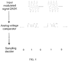
- FIG. 4 illustrates a demodulation process of a 2ASK modulated signal by the analog voltage comparator 21.
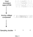
- FIG. 5 illustrates a demodulation process of a 2FSK modulated signal by the analog voltage comparator.
- FIG. 6 illustrates a demodulation process of a 2PSK modulated signal by the analog voltage comparator.
- the comparator threshold voltage is half of a peak voltage of the modulated signal, and the specific value of the comparator threshold voltage may be adjusted according to an application scenario of the signal demodulation apparatus.
- the signal demodulation apparatus includes an analog voltage comparator 21 and a sampling decider 22.
- the sampling decider 22 includes:
- the high-frequency clock sampling circuit samples at least two points for a high level of any pulse of the digital signal using the high-frequency clock; the sampled digital signal is a contiguous binary code stream; and a feature extracting and deciding circuit 222, configured to extract the feature of the sampled digital signal, and compare the feature extracted with features of known digital modulated signals to acquire the value represented by the digital signal to complete signal demodulation.
- the feature includes at least one of: a detection pulse width, a period, a rising edge, and a falling edge of the sampled digital signal.
- the feature extracted are compared with features of known digital modulated signals to acquire the value represented by the digital signal, as illustrated in FIG. 4 to FIG. 6 , to complete signal demodulation.
- the signal demodulation method includes:
- the present application employs a simple circuit structure to demodulate the modulated signal in a closed communication system, and has the advantages of simple circuit structure, easy to implement, small circuit area, low power consumption and the like. Accordingly, the technical solutions according to the present application are suitable for a scenario imposing strict requirements on the power consumption and area, for example, a wearable device and the like.
- the signal demodulation method includes step S1 and step S2.
- step S1 includes:
- Step S13 specifically includes: outputting a digital signal having a first value if a voltage of the modulated signal is greater than the comparator threshold voltage; and otherwise, outputting a digital signal having a second value.
- the first value is 1, and the second value is 0.
- the comparator threshold voltage of the analog voltage comparator only needs to be set to a suitable value.
- common digital signals such as 2ASK, 2FSK, 2PSK and the like passes through the analog voltage comparator, that is, after the modulated signal is compared with the comparator threshold voltage, value 0 and value 1 both have different apparent features. Therefore, the digital signal composed of 1 or 0 output by the signal output terminal 213 of the analog voltage comparator 21 may be acquired according to the different apparent features.
- FIG. 4 illustrates a demodulation process of a 2ASK modulated signal by the analog voltage comparator 21.
- FIG. 5 illustrates a demodulation process of a 2FSK modulated signal by the voltage comparator.
- FIG. 6 illustrates a demodulation process of a 2PSK modulated signal by the voltage comparator.
- the comparator threshold voltage is half of a peak voltage of the modulated signal, and the specific value of the comparator threshold voltage may be adjusted according to an application scenario of the signal demodulation apparatus.
- the signal demodulation method includes step S1 and step S2.
- step S2 includes: S21: Sampling the digital signal using a high-frequency clock.
- a frequency of the high-frequency clock is determined according to a pulse width of the digital signal and an application scenario of the signal demodulation apparatus.
- the high-frequency clock sampling circuit samples at least two points for a high level of any pulse of the digital signal using the high-frequency clock.
- the sampled digital signal is a contiguous binary code stream.
- the feature includes at least one of: a detection pulse width, a period, a rising edge, and a falling edge of the sampled digital signal.
- the feature extracted are compared with features of known digital modulated signal to acquire the value represented by the digital signal, as illustrated in FIG. 4 to FIG. 6 , to complete signal demodulation.
- modules in the devices according to the embodiments may be adaptively modified and these modules may be configured in one or more devices different from the embodiments herein.
- Modules or units or components in the embodiments may be combined into a single module or unit or component, and additionally these modules, units or components may be practiced in a plurality of sub-modules, subunits or subcomponents.
- all the features disclosed in this specification including the appended claims, abstract and accompanying drawings
- all the processes or units in such disclosed methods or devices may be combined in any way.
- Embodiments of the individual components of the present application may be implemented in hardware, or in a software module running one or more processors, or in a combination thereof. It will be appreciated by those skilled in the art that, in practice, some or all of the functions of some or all of the components in the message prompting apparatus according to individual embodiments of the present application may be implemented using a microprocessor or a digital signal processor (DSP).
- DSP digital signal processor
- the present application may also be implemented as an apparatus of a device program (e.g., a computer program and a computer program product) for performing a part or all of the method as described herein.
- Such a program implementing the present application may be stored on a computer readable medium, or may be stored in the form of one or more signals. Such a signal may be obtained by downloading it from an Internet website, or provided on a carrier signal, or provided in any other form.
- any reference sign placed between the parentheses shall not be construed as a limitation to a claim.
- the word “comprise” does not exclude the presence of an element or a step not listed in a claim.
- the word “a” or “an” used before an element does not exclude the presence of a plurality of such elements.
- the present application may be implemented by means of a hardware comprising several distinct elements and by means of a suitably programmed computer. In a unit claim enumerating several devices, several of the devices may be embodied by one and the same hardware item. Use of the words “first”, “second”, “third” and the like does not mean any ordering. Such words may be construed as naming.
Landscapes
- Engineering & Computer Science (AREA)
- Computer Networks & Wireless Communication (AREA)
- Signal Processing (AREA)
- Digital Transmission Methods That Use Modulated Carrier Waves (AREA)
- Circuits Of Receivers In General (AREA)
Abstract
Description
- The present application relates to the technical field of signal demodulation, and in particular, relates to a signal demodulation apparatus and method in a closed communication system.
- Common digital modulation is implemented by binary amplitude shift keying (2ASK), binary frequency shift keying (2FSK), binary phase shift keying (2PSK) and the like; and corresponding demodulation is implemented by filtering, envelop detection, local carrier multiplication, sampling decision and the like.
- In a non-closed communication system, since a receiving end has no knowledge of the modulation mode of a transmitting end, a complicated demodulation circuit needs to be configured in order to prevent interference caused by other modulated signals to modulated signals that need to be demodulated.
- Referring to
FIG. 1 , in a typical 2FSK demodulation method, four filters, two envelop detectors and one sampling decider need to be configured in order to prevent interference caused by 2ASK, 2PSK and other modulated signals to the 2FSK modulated signal. This demodulation method is very complicated, and implementation of this method requires a large circuit area and a high power consumption. Therefore, this method fails to accommodate application of ultra-low power consumption. In a closed communication system, since the receiving end acknowledges the modulation manner of the transmitting end, including amplitude, frequency, length and the like information of the carrier, the receiving end may only receive a specific type of modulated signals. Therefore, unlike the scenario of a non-closed communication system, it is unnecessary to consider interference caused by other modulated signals like. - As seen from the above, a closed communication system has the characteristics of single communication signal, fixed modulation manner, and limited power consumption. If the signal demodulation apparatus for a conventional communication system is applied to a closed communication system, an apparatus with a complicated circuit needs to be further configured, which consequently increases power consumption of the communication system.
- Therefore, a signal demodulation apparatus for a closed communication system is urgently desired to solve the problem in the prior art.
- In view of the above problem, the present application provides a signal demodulation apparatus and method in a closed communication system to solve or partially solve the above problem.
- In one aspect, the present application provides a signal demodulation apparatus for a closed communication system. The signal demodulation apparatus includes:
- an analog voltage comparator, configured to convert a received modulated signal into a digital signal, and output the digital signal; and
- a sampling decider, configured to sample the received digital signal, and acquire a value represented by the digital signal according to a feature of a sampled digital signal to complete a signal demodulation.
- In another aspect, the present application provides a signal demodulation method in a closed communication system. The signal demodulation method includes:
- converting a received modulated signal into a digital signal; and
- sampling the received digital signal, and acquiring a value represented by the digital signal according to a feature of a sampled digital signal to complete a signal demodulation.
- With the signal demodulation apparatus and method in a closed communication system according to the present application, an analog voltage comparator converts a modulated analog signal into a digital signal; and a sampling decider samples the digital signal and makes a feature judgment to acquire a value represented by the digital signal to complete the signal demodulation. Therefore, the present application employs a simple circuit structure to demodulate the modulated signal in a closed communication system, and may have the advantages of simple circuit structure, easy to implement, small circuit area, low power consumption and the like. Accordingly, the technical solutions according to the present application are suitable for a scenario imposing strict requirements on the power consumption and area, for example, a wearable device and the like.
- The above description only summarizes the technical solutions of the present application. Specific embodiments of the present application are described hereinafter to better and clearer understand the technical solutions of the present application, to practice the technical solutions based on the disclosure of the specification and to make the above and other objectives, features and advantages of the present application more apparent and understandable.
- By reading the detailed description of preferred embodiments hereinafter, various other advantages and beneficial effects become clear and apparent for persons of ordinary skill in the art. The accompanying drawings are merely for illustrating the preferred embodiments, but shall not be construed as limiting the present application. In all the accompanying drawings, like reference signs denote like parts. In the drawings:
-
FIG. 1 is a schematic diagram of a conventional 2FSK demodulation circuit; -
FIG. 2 is a schematic diagram of a signal demodulation apparatus for a closed communication system according to one embodiment of the present application; -
FIG. 3 is a schematic diagram of an analog voltage comparator of the signal demodulation apparatus for the closed communication system according to one embodiment of the present application; -
FIG. 4 is a schematic diagram of demodulation of an input 2ASK modulated signal by an analog voltage comparator and a sampling decider; -
FIG. 5 is a schematic diagram of demodulation of an input 2FSK modulated signal by an analog voltage comparator and a sampling decider; -
FIG. 6 is a schematic diagram of demodulation of an input 2PSK modulated signal by an analog voltage comparator and a sampling decider; -
FIG. 7 is a schematic diagram of a sampling decider of the signal demodulation apparatus for the closed communication system according to one embodiment of the present application; -
FIG. 8 is a flowchart of a signal demodulation method applied in a closed communication system according to one embodiment of the present application; -
FIG. 9 is a flowchart of step S1 of the signal demodulation method applied in a closed communication system according to one embodiment of the present application; and -
FIG. 10 is a flowchart of step S2 of the signal demodulation method applied in a closed communication system according to one embodiment of the present application. - Some exemplary embodiments of the present application are hereinafter described in detail with reference to the accompanying drawings. Although the accompanying drawings illustrate the exemplary embodiments of the present application, it shall be understood that the present application may be practiced in various manners, and the present application shall not be limited by the embodiments illustrated herein. On the contrary, these embodiments are described herein only for the purpose of better understanding the present application, and may integrally convey the scope of the present application to a person skilled in the art.
- Referring to
FIG. 2 , one embodiment of the present application provides a signal demodulation apparatus for a closed communication system. The signal demodulation apparatus includes: - an
analog voltage comparator 21, configured to convert a received modulated signal into a digital signal, and output the digital signal; and - a
sampling decider 22, configured to sample the received digital signal, and acquire a value represented by the digital signal according to a feature of a sampled digital signal to complete a signal demodulation. - The present application employs a simple circuit structure to demodulate the modulated signal in a closed communication system, and has the advantages of simple circuit structure, easy to implement, small circuit area, low power consumption and the like. Accordingly, the technical solutions according to the present application are suitable for a scenario imposing strict requirements on the power consumption and area, for example, a wearable device and the like.
- Another embodiment of the present application provides a signal demodulation apparatus for a closed communication system. The signal demodulation apparatus includes an
analog voltage comparator 21 and asampling decider 22. - Referring to
FIG. 3 , theanalog voltage comparator 21 includes: - a
signal input terminal 211, configured to receive the modulated signal; - a
threshold input terminal 212, configured to receive a comparator threshold voltage; and - a
signal output terminal 213, configured to output a digital signal according to a comparison result between the modulated signal and the comparator threshold voltage. - The
signal output terminal 213 is specifically configured to: output a digital signal having a first value if a voltage of the modulated signal is greater than the comparator threshold voltage; and otherwise, output a digital signal having a second value. - Specifically, the first value is 1, and the second value is 0.
- When the modulated signal received by the
signal input terminal 211 passes through theanalog voltage comparator 21, the comparator threshold voltage of theanalog voltage comparator 21 only needs to be set to a suitable value. After common digital modulated signals such as 2ASK, 2FSK, 2PSK and the like passes through theanalog voltage comparator 21, that is, after the modulated signal is compared with the comparator threshold voltage,value 0 andvalue 1 both have different apparent features. Therefore, the digital signal composed of 1 or 0 output by thesignal output terminal 213 of theanalog voltage comparator 21 may be acquired according to the different apparent features. -
FIG. 4 illustrates a demodulation process of a 2ASK modulated signal by theanalog voltage comparator 21.FIG. 5 illustrates a demodulation process of a 2FSK modulated signal by the analog voltage comparator.FIG. 6 illustrates a demodulation process of a 2PSK modulated signal by the analog voltage comparator. As seen from the above drawings, with respect to a particular digital modulated signal, after the digital signal passes through theanalog voltage comparator 21, the acquired square waves all have different apparent features. After the 2ASK modulated signal is demodulated by the analog voltage comparator, a high square wave representsvalue 1, and a low square wave value representsvalue 0. After the 2FSK modulated signal is demodulated by the analog voltage comparator, compact square waves representvalue 1, and sparse square waves representvalue 0. After the 2PSK modulated signal is demodulated by the analog voltage comparator, a cosine wave representsvalue 1, and a sine wave representsvalue 0. The digital signal composed of 1 or 0 output by thesignal output terminal 213 of theanalog voltage comparator 21 is acquired according to the above features. - To achieve an ideal demodulation effect, the comparator threshold voltage is half of a peak voltage of the modulated signal, and the specific value of the comparator threshold voltage may be adjusted according to an application scenario of the signal demodulation apparatus.
- Another embodiment of the present application provides a signal demodulation apparatus for a closed communication system. The signal demodulation apparatus includes an
analog voltage comparator 21 and asampling decider 22. - Referring to
FIG. 7 , thesampling decider 22 includes: - a high-frequency
clock sampling circuit 221, configured to sample the digital signal using a high-frequency clock, and output a sampled digital signal; and - specifically, a frequency of the high-frequency clock is determined according to a pulse width of the digital signal and an application scenario of the signal demodulation apparatus.
- To achieve an ideal demodulation effect, the high-frequency clock sampling circuit samples at least two points for a high level of any pulse of the digital signal using the high-frequency clock;
the sampled digital signal is a contiguous binary code stream; and
a feature extracting and decidingcircuit 222, configured to extract the feature of the sampled digital signal, and compare the feature extracted with features of known digital modulated signals to acquire the value represented by the digital signal to complete signal demodulation. - The feature includes at least one of: a detection pulse width, a period, a rising edge, and a falling edge of the sampled digital signal.
- The feature extracted are compared with features of known digital modulated signals to acquire the value represented by the digital signal, as illustrated in
FIG. 4 to FIG. 6 , to complete signal demodulation. - Referring to
FIG. 8 , one embodiment of the present application provides a signal demodulation method applied in a closed communication system. The signal demodulation method includes: - S1: converting a received modulated signal into a digital signal; and
- S2: sampling the received digital signal, and acquiring a value represented by the digital signal according to a feature of a sampled digital signal to complete a signal demodulation.
- The present application employs a simple circuit structure to demodulate the modulated signal in a closed communication system, and has the advantages of simple circuit structure, easy to implement, small circuit area, low power consumption and the like. Accordingly, the technical solutions according to the present application are suitable for a scenario imposing strict requirements on the power consumption and area, for example, a wearable device and the like.
- Another embodiment of the present application provides a signal demodulation method in a closed communication system. The signal demodulation method includes step S1 and step S2.
- Referring to
FIG. 9 , step S1 includes: - S11: receiving the modulated signal;
- S12: receiving a comparator threshold voltage; and
- S13: outputting a digital signal according to a comparison result between the modulated signal and the comparator threshold voltage.
- Step S13 specifically includes: outputting a digital signal having a first value if a voltage of the modulated signal is greater than the comparator threshold voltage; and otherwise, outputting a digital signal having a second value.
- Specifically, the first value is 1, and the second value is 0.
- When the received modulated signal passes through the analog voltage comparator, the comparator threshold voltage of the analog voltage comparator only needs to be set to a suitable value. After common digital signals such as 2ASK, 2FSK, 2PSK and the like passes through the analog voltage comparator, that is, after the modulated signal is compared with the comparator threshold voltage,
value 0 andvalue 1 both have different apparent features. Therefore, the digital signal composed of 1 or 0 output by thesignal output terminal 213 of theanalog voltage comparator 21 may be acquired according to the different apparent features. -
FIG. 4 illustrates a demodulation process of a 2ASK modulated signal by theanalog voltage comparator 21.FIG. 5 illustrates a demodulation process of a 2FSK modulated signal by the voltage comparator.FIG. 6 illustrates a demodulation process of a 2PSK modulated signal by the voltage comparator. As seen from the above drawings, with respect to a particular digital modulated signal, after the digital signal passes through theanalog voltage comparator 21,value 0 andvalue 1 both have different apparent features. Accordingly, the digital signal composed of 1 or 0 output by thesignal output terminal 213 of theanalog voltage comparator 21 is acquired according to the above features. - To achieve an ideal demodulation effect, the comparator threshold voltage is half of a peak voltage of the modulated signal, and the specific value of the comparator threshold voltage may be adjusted according to an application scenario of the signal demodulation apparatus.
- Another embodiment of the present application provides a signal demodulation method in a closed communication system. The signal demodulation method includes step S1 and step S2.
- Referring to
FIG. 10 , step S2 includes:
S21: Sampling the digital signal using a high-frequency clock. - Specifically, a frequency of the high-frequency clock is determined according to a pulse width of the digital signal and an application scenario of the signal demodulation apparatus.
- To achieve an ideal demodulation effect, the high-frequency clock sampling circuit samples at least two points for a high level of any pulse of the digital signal using the high-frequency clock.
- The sampled digital signal is a contiguous binary code stream.
- S22: Extracting the feature of the sampled digital signal, and comparing the feature extracted with features of known digital modulated signals to acquire the value represented by the digital signal to complete signal demodulation.
- The feature includes at least one of: a detection pulse width, a period, a rising edge, and a falling edge of the sampled digital signal.
- The feature extracted are compared with features of known digital modulated signal to acquire the value represented by the digital signal, as illustrated in
FIG. 4 to FIG. 6 , to complete signal demodulation. - The algorithms and displays provided herein are not inherently related to any specific computer, virtual system or other device. Various general-purpose systems may also be used with the teachings herein. According to the above description, the structure required for constructing such systems is obvious. In addition, the present application is not directed to any specific programming language. It should be understood that the content of the present application described herein may be carried out utilizing various programming languages, and that the above description for a specific language is for the sake of disclosing preferred embodiments of the present application.
- In the specification provided herein, a plenty of particular details are described. However, it can be appreciated that an embodiment of the present application may also be practiced without these particular details. In some embodiments, well known methods, structures and technologies are not illustrated in detail so as not to obscure the understanding of the specification.
- Likewise, it shall be understood that, to streamline the present application and facilitate understanding of one or more of various aspects of the present application, in the above description of the exemplary embodiments of the present application, various features of the present application are sometimes incorporated in an individual embodiment, drawing or description thereof. However, the method according to the present application shall not be explained to embody the following intension: the present application seeking protection claims more features than those explicitly disclosed in each of the appended claims. To be more exact, as embodied in the appended claims, the inventive aspects lie in that fewer features than all the features embodied in an individual embodiment as described above. Therefore, the claims observing the specific embodiments are herein incorporated into the specific embodiments, and each claim may be deemed as an individual embodiment of the present application.
- Those skilled in the art should understand that modules in the devices according to the embodiments may be adaptively modified and these modules may be configured in one or more devices different from the embodiments herein. Modules or units or components in the embodiments may be combined into a single module or unit or component, and additionally these modules, units or components may be practiced in a plurality of sub-modules, subunits or subcomponents. Besides that such features and/or processes or at least some of the units are mutually exclusive, all the features disclosed in this specification (including the appended claims, abstract and accompanying drawings) and all the processes or units in such disclosed methods or devices may be combined in any way. Unless otherwise stated, each of the features disclosed in this specification (including the appended claims, abstract and accompanying drawings) may be replaced by a provided same, equivalent or similar substitution.
- In addition, those skilled in the art shall understand that, although some embodiments described herein include some features included in other embodiments, rather than other features, a combination of the features in different embodiments signifies that the features are within the scope of the present application and different embodiments may be derived. For example, in the claims appended hereinafter, any one of the embodiments seeking protection may be practiced in any combination manner.
- Embodiments of the individual components of the present application may be implemented in hardware, or in a software module running one or more processors, or in a combination thereof. It will be appreciated by those skilled in the art that, in practice, some or all of the functions of some or all of the components in the message prompting apparatus according to individual embodiments of the present application may be implemented using a microprocessor or a digital signal processor (DSP). The present application may also be implemented as an apparatus of a device program (e.g., a computer program and a computer program product) for performing a part or all of the method as described herein. Such a program implementing the present application may be stored on a computer readable medium, or may be stored in the form of one or more signals. Such a signal may be obtained by downloading it from an Internet website, or provided on a carrier signal, or provided in any other form.
- Reference herein to "one embodiment", "an embodiment" or to "one or more embodiments" implies that a particular feature, structure, or characteristic described in connection with the embodiments is included in at least one embodiment of the present application. Further, it should be noted that instances of the phrase "in one embodiment" herein are not necessarily all referring to the same embodiment.
- In the specification provided herein, a plenty of particular details are described. However, it can be appreciated that an embodiment of the present application may also be practiced without these particular details. In some embodiments, well known methods, structures and technologies are not illustrated in detail so as not to obscure the understanding of the specification.
- It should be noted that the above embodiments illustrate rather than limit the present application, and those skilled in the art may design alternative embodiments without departing from the scope of the appended claims. In the claims, any reference sign placed between the parentheses shall not be construed as a limitation to a claim. The word "comprise" does not exclude the presence of an element or a step not listed in a claim. The word "a" or "an" used before an element does not exclude the presence of a plurality of such elements. The present application may be implemented by means of a hardware comprising several distinct elements and by means of a suitably programmed computer. In a unit claim enumerating several devices, several of the devices may be embodied by one and the same hardware item. Use of the words "first", "second", "third" and the like does not mean any ordering. Such words may be construed as naming.
Claims (20)
- A signal demodulation apparatus for a closed communication system, comprising:an analog voltage comparator, configured to convert a received modulated signal into a digital signal, and output the digital signal; anda sampling decider, configured to sample the received digital signal, and acquire a value represented by the digital signal according to a feature of a sampled digital signal to complete a signal demodulation.
- The signal demodulation apparatus for a closed communication system according to claim 1, wherein the analog voltage comparator comprises:a signal input terminal, configured to receive the modulated signal;a threshold input terminal, configured to receive a comparator threshold voltage; anda signal output terminal, configured to output a digital signal according to a comparison result between the modulated signal and the comparator threshold voltage.
- The signal demodulation apparatus for a closed communication system according to claim 2, wherein the signal output terminal is configured to: output a digital signal having a first value if a voltage of the modulated signal is greater than the comparator threshold voltage; and otherwise, output a digital signal having a second value.
- The signal demodulation apparatus for a closed communication system according to claim 3, wherein the first value is 1 and the second value is 0.
- The signal demodulation apparatus for a closed communication system according to any one of claims 2 to 4, wherein the comparator threshold voltage is half of a peak voltage of the modulated signal.
- The signal demodulation apparatus for a closed communication system according to claim 1, wherein the sampling decider comprises:a high-frequency clock sampling circuit, configured to sample the digital signal using a high-frequency clock, and output the sampled digital signal; anda feature extracting and deciding circuit, configured to extract the feature of the sampled digital signal, and compare the feature extracted with features of known digital modulated signals to acquire the value represented by the digital signal to complete a signal demodulation.
- The signal demodulation apparatus for a closed communication system according to claim 6, wherein a frequency of the high-frequency clock is determined according to a pulse width of the digital signal and an application scenario of the signal demodulation apparatus.
- The signal demodulation apparatus for a closed communication system according to claim 7, wherein the high-frequency clock sampling circuit samples at least two points for a high level of any pulse of the digital signal using the high-frequency clock.
- The signal demodulation apparatus for a closed communication system according to claim 8, wherein the sampled digital signal is a contiguous binary code stream.
- The signal demodulation apparatus for a closed communication system according to claim 6, wherein the feature comprises at least one of: a detection pulse width, a period, a rising edge, and a falling edge of the sampled digital signal.
- A signal demodulation method in a closed communication system, comprising:converting a received modulated signal into a digital signal; andsampling the received digital signal, and acquiring a value represented by the digital signal according to a feature of a sampled digital signal to complete a signal demodulation.
- The signal demodulation method in a closed communication system according to claim 11, wherein the converting a received modulated signal into a digital signal comprises:receiving the modulated signal;receiving a comparator threshold voltage; andoutputting a digital signal according to a comparison result between the modulated signal and the comparator threshold voltage.
- The signal demodulation method in a closed communication system according to claim 12, wherein the outputting a digital signal according to a comparison result between the modulated signal and the comparator threshold voltage comprises: outputting a digital signal having a first value if a voltage of the modulated signal is greater than the comparator threshold voltage; and otherwise, outputting a digital signal having a second value.
- The signal demodulation method in a closed communication system according to claim 13, wherein the first value is 1 and the second value is 0.
- The signal demodulation method in a closed communication system according to any one of claims 12 to 14, wherein the comparator threshold voltage is half of a peak voltage of the modulated signal.
- The signal demodulation method in a closed communication system according to claim 11, wherein sampling the received digital signal, and acquiring a value represented by the digital signal according to a feature of a sampled digital signal to complete signal demodulation comprises:sampling the received digital signal using a high-frequency clock; andextracting the feature of the sampled digital signal, and comparing the feature extracted with features of known digital modulated signals to acquire the value represented by the digital signal to complete a signal demodulation.
- The signal demodulation method in a closed communication system according to claim 16, wherein a frequency of the high-frequency clock is determined according to a pulse width of the digital signal and an application scenario of the signal demodulation apparatus.
- The signal demodulation method in a closed communication system according to claim 17, wherein the high-frequency clock sampling circuit samples at least two points for a high level of any pulse of the digital signal using the high-frequency clock.
- The signal demodulation method in a closed communication system according to claim 18, wherein the sampled digital signal is a contiguous binary code stream.
- The signal demodulation method in a closed communication system according to claim 16, wherein the feature comprises at least one of: a detection pulse width, a period, a rising edge, and a falling edge of the sampled digital signal.
Applications Claiming Priority (1)
| Application Number | Priority Date | Filing Date | Title |
|---|---|---|---|
| PCT/CN2016/089742 WO2018010082A1 (en) | 2016-07-12 | 2016-07-12 | Signal demodulating device and method applying to closed communication system |
Publications (3)
| Publication Number | Publication Date |
|---|---|
| EP3324590A1 true EP3324590A1 (en) | 2018-05-23 |
| EP3324590A4 EP3324590A4 (en) | 2018-09-12 |
| EP3324590B1 EP3324590B1 (en) | 2019-12-18 |
Family
ID=58215698
Family Applications (1)
| Application Number | Title | Priority Date | Filing Date |
|---|---|---|---|
| EP16886811.5A Active EP3324590B1 (en) | 2016-07-12 | 2016-07-12 | Signal demodulating device and method applying to closed communication system |
Country Status (5)
| Country | Link |
|---|---|
| US (2) | US10291388B2 (en) |
| EP (1) | EP3324590B1 (en) |
| KR (1) | KR20180116119A (en) |
| CN (1) | CN106464624B (en) |
| WO (1) | WO2018010082A1 (en) |
Families Citing this family (9)
| Publication number | Priority date | Publication date | Assignee | Title |
|---|---|---|---|---|
| CN108055220B (en) * | 2017-12-12 | 2020-09-29 | 成都宝通天宇电子科技有限公司 | ASK amplitude self-adaptive anti-noise demodulation method and device |
| US12327980B2 (en) | 2019-08-20 | 2025-06-10 | Sony Semiconductor Solutions Corporation | Semiconductor laser driving apparatus, electronic equipment, and manufacturing method of semiconductor laser driving apparatus |
| CN110611514B (en) * | 2019-09-20 | 2022-05-17 | 内蒙古信元网络安全技术股份有限公司 | Signal demodulation system, method and computer storage medium for distributed receiver |
| US10892800B1 (en) | 2020-01-06 | 2021-01-12 | Nucurrent, Inc. | Systems and methods for wireless power transfer including pulse width encoded data communications |
| US11303164B2 (en) * | 2020-07-24 | 2022-04-12 | Nucurrent, Inc. | Low cost communications demodulation for wireless power transmission system |
| US11303165B2 (en) * | 2020-07-24 | 2022-04-12 | Nucurrent, Inc. | Low cost communications demodulation for wireless power receiver system |
| US11277035B1 (en) | 2021-02-01 | 2022-03-15 | Nucurrent, Inc. | Automatic gain control for communications demodulation in wireless power transmitters |
| US11811244B2 (en) | 2021-02-01 | 2023-11-07 | Nucurrent, Inc. | Automatic gain control for communications demodulation in wireless power transmitters |
| CN113395070B (en) * | 2021-04-12 | 2024-02-09 | 上海昱章电气股份有限公司 | Analog signal processing method and device and computer equipment |
Family Cites Families (32)
| Publication number | Priority date | Publication date | Assignee | Title |
|---|---|---|---|---|
| US4065722A (en) * | 1976-12-27 | 1977-12-27 | Glenayre Electronics, Ltd. | Demodulation method and circuit for discretely modulated ac signals |
| JPH03101546A (en) * | 1989-09-14 | 1991-04-26 | Matsushita Electric Works Ltd | Digital signal read system |
| US5107522A (en) * | 1990-02-05 | 1992-04-21 | Sharp Kabushiki Kaisha | Automatic frequency control circuit |
| US5550505A (en) * | 1994-12-30 | 1996-08-27 | General Electric Company | Frequency shift keying (FSK) demodulator for use in low signal-to-noise ratio environments |
| JP3108364B2 (en) * | 1996-04-22 | 2000-11-13 | 三洋電機株式会社 | Data demodulator |
| DE69732601T2 (en) * | 1996-05-28 | 2006-04-06 | Koninklijke Philips Electronics N.V. | RECEIVER, DEMODULATOR AND DEMODULATION METHOD |
| KR100290284B1 (en) | 1997-11-18 | 2001-05-15 | 윤종용 | Fsk demodulator having counter |
| JP3252820B2 (en) * | 1999-02-24 | 2002-02-04 | 日本電気株式会社 | Demodulation and modulation circuit and demodulation and modulation method |
| JP2000307665A (en) * | 1999-04-22 | 2000-11-02 | Matsushita Electric Ind Co Ltd | Demodulation circuit and demodulation method for wireless receiving device |
| JP3783853B2 (en) * | 2002-02-12 | 2006-06-07 | 株式会社ゼネラル リサーチ オブ エレクトロニックス | Center level detection correction circuit for FSK demodulated signal |
| CN100499619C (en) * | 2004-04-05 | 2009-06-10 | 鼎芯通讯(上海)有限公司 | Binary frequency shift keying demodulator |
| JP4506426B2 (en) * | 2004-11-19 | 2010-07-21 | ソニー株式会社 | COFDM modulation receiver and adjacent channel interference elimination method |
| CN100496033C (en) * | 2006-03-23 | 2009-06-03 | 上海交通大学 | Demodulation Method of Binary Frequency Shift Keying System Based on Hilbert-Huang Transform |
| EP1848105B1 (en) * | 2006-04-21 | 2008-08-06 | Alcatel Lucent | Data slicer circuit, demodulation stage, receiving system and method for demodulating shift keying coded signals |
| CN1953438A (en) * | 2006-10-26 | 2007-04-25 | 西安电子科技大学 | Binary frequency shift key controlled filling type digital demodulation method |
| US20080252367A1 (en) * | 2007-04-10 | 2008-10-16 | Micrel, Inc. | Demodulator with Multiple Operating Modes for Amplitude Shift Keyed Signals |
| US7633320B2 (en) * | 2007-06-29 | 2009-12-15 | Kabushiki Kaisha Toshiba | Comparator circuit |
| US7885359B2 (en) * | 2007-08-15 | 2011-02-08 | Seiko Epson Corporation | Sampling demodulator for amplitude shift keying (ASK) radio receiver |
| JP2009055097A (en) * | 2007-08-23 | 2009-03-12 | Advanced Telecommunication Research Institute International | FSK demodulation circuit and method |
| CN101729470A (en) * | 2008-10-24 | 2010-06-09 | 南京师范大学 | Constant amplitude and period digital signal modulation and demodulation method |
| CN102123122B (en) * | 2010-01-07 | 2013-10-16 | 无锡爱睿芯电子有限公司 | Modulation-demodulation device and modulation-demodulation method |
| CN201607480U (en) * | 2009-11-13 | 2010-10-13 | 英业达股份有限公司 | Power Signal Test Set |
| CN102014093B (en) * | 2010-12-09 | 2012-12-19 | 东南大学 | Extended binary phase shift keying (EBPSK) modem and implementation method thereof |
| TWI514777B (en) * | 2012-08-03 | 2015-12-21 | Realtek Semiconductor Corp | Predictive successive-approximation-register converting device and method therefor |
| CN103346988B (en) * | 2013-06-13 | 2016-03-23 | 电子科技大学 | A kind of FSK digital demodulator |
| CN103634263A (en) * | 2013-12-07 | 2014-03-12 | 天津光电通信技术有限公司 | Continuous-phase frequency-shift keying digital demodulation device and demodulation method implemented by same |
| CN104300984B (en) * | 2014-10-21 | 2018-04-27 | 上海玮舟微电子科技有限公司 | A kind of analog-digital converter and D conversion method |
| CN105897639B (en) * | 2014-12-09 | 2020-06-16 | 恩智浦美国有限公司 | FSK demodulator |
| CN104793680B (en) * | 2015-04-08 | 2017-12-12 | 云南卓烁科技有限公司 | A kind of voltage signal demodulator circuit |
| US9531400B1 (en) * | 2015-11-04 | 2016-12-27 | Avnera Corporation | Digitally calibrated successive approximation register analog-to-digital converter |
| CN107040260B (en) * | 2016-02-03 | 2020-09-08 | 中芯国际集成电路制造(上海)有限公司 | Asynchronous successive approximation type analog-to-digital conversion circuit |
| US9584144B1 (en) * | 2016-04-21 | 2017-02-28 | Xilinx, Inc. | Asynchronous clock generation for time-interleaved successive approximation analog to digital converters |
-
2016
- 2016-07-12 EP EP16886811.5A patent/EP3324590B1/en active Active
- 2016-07-12 WO PCT/CN2016/089742 patent/WO2018010082A1/en not_active Ceased
- 2016-07-12 CN CN201680000578.4A patent/CN106464624B/en not_active Expired - Fee Related
- 2016-07-12 KR KR1020177021643A patent/KR20180116119A/en not_active Ceased
-
2017
- 2017-07-30 US US15/663,807 patent/US10291388B2/en active Active
-
2019
- 2019-02-22 US US16/283,698 patent/US10523410B2/en active Active
Also Published As
| Publication number | Publication date |
|---|---|
| US10523410B2 (en) | 2019-12-31 |
| US20190207741A1 (en) | 2019-07-04 |
| CN106464624B (en) | 2019-04-09 |
| US20180026780A1 (en) | 2018-01-25 |
| KR20180116119A (en) | 2018-10-24 |
| WO2018010082A1 (en) | 2018-01-18 |
| EP3324590B1 (en) | 2019-12-18 |
| EP3324590A4 (en) | 2018-09-12 |
| US10291388B2 (en) | 2019-05-14 |
| CN106464624A (en) | 2017-02-22 |
Similar Documents
| Publication | Publication Date | Title |
|---|---|---|
| US10523410B2 (en) | Signal demodulation apparatus and method in closed communication system | |
| CN108512791B (en) | Satellite-borne AIS demodulation method based on timing frequency offset compensation | |
| WO2017082817A1 (en) | Apparatus and method for direct radio frequency (rf) sampling in near field communication (nfc) devices | |
| US20170070265A1 (en) | Wireless charger using frequency aliasing fsk demodulation | |
| US12196880B2 (en) | Method and apparatus for detecting and characterizing pulse sequences | |
| CN106059969A (en) | Modulation identification method and device based on envelope square spectrum analysis | |
| CN100496033C (en) | Demodulation Method of Binary Frequency Shift Keying System Based on Hilbert-Huang Transform | |
| CN104156760B (en) | Electronic tag and detuner thereof | |
| CN105743830B (en) | A kind of demodulation method of MFSK signals | |
| CN114266264B (en) | Signal demodulation method, device, receiver and computer-readable storage medium | |
| CN107404452A (en) | BPSK demodulation methods and device, receiver | |
| US9941862B2 (en) | Filter that minimizes in-band noise and maximizes detection sensitivity of exponentially-modulated signals | |
| US20190260357A1 (en) | Filter that minimizes in-band noise and maximizes detection sensitivity of exponentially-modulated signals | |
| CN102904847A (en) | Double denoising signal modulation identification method based on instantaneous information | |
| Bae et al. | Locally optimum rank detector test statistics for composite signals in generalized observations: One-sample case | |
| CN109639286A (en) | A kind of IRIG-B adaptive decoding circuit and method | |
| CN106027165B (en) | OOK pulsed signals device, method and communicator | |
| Sakhawat et al. | Communication intelligence (COMINT) signal processor: A physical realization | |
| CN104299617A (en) | Method for inlaying and detecting digital information in audio frequency | |
| Kostanic et al. | Independent component analysis based QAM receiver | |
| Rangarao et al. | A robust BFSK signal demodulator using Orthogonal Decomposer | |
| CN205883254U (en) | OOK impulse signal reception device and communication device | |
| WO2025001829A1 (en) | Subcarrier modulation method and device for optical module oam data, and subcarrier demodulation method and device for optical module oam data | |
| CN102158439B (en) | Coherent detection method and device | |
| CN116886485A (en) | Integrated communication perception method, system, device and medium based on LoRa signal |
Legal Events
| Date | Code | Title | Description |
|---|---|---|---|
| STAA | Information on the status of an ep patent application or granted ep patent |
Free format text: STATUS: UNKNOWN |
|
| STAA | Information on the status of an ep patent application or granted ep patent |
Free format text: STATUS: THE INTERNATIONAL PUBLICATION HAS BEEN MADE |
|
| PUAI | Public reference made under article 153(3) epc to a published international application that has entered the european phase |
Free format text: ORIGINAL CODE: 0009012 |
|
| STAA | Information on the status of an ep patent application or granted ep patent |
Free format text: STATUS: REQUEST FOR EXAMINATION WAS MADE |
|
| 17P | Request for examination filed |
Effective date: 20170801 |
|
| AK | Designated contracting states |
Kind code of ref document: A1 Designated state(s): AL AT BE BG CH CY CZ DE DK EE ES FI FR GB GR HR HU IE IS IT LI LT LU LV MC MK MT NL NO PL PT RO RS SE SI SK SM TR |
|
| AX | Request for extension of the european patent |
Extension state: BA ME |
|
| R17P | Request for examination filed (corrected) |
Effective date: 20170801 |
|
| A4 | Supplementary search report drawn up and despatched |
Effective date: 20180814 |
|
| RIC1 | Information provided on ipc code assigned before grant |
Ipc: H04L 27/06 20060101AFI20180808BHEP |
|
| STAA | Information on the status of an ep patent application or granted ep patent |
Free format text: STATUS: EXAMINATION IS IN PROGRESS |
|
| 17Q | First examination report despatched |
Effective date: 20190403 |
|
| GRAP | Despatch of communication of intention to grant a patent |
Free format text: ORIGINAL CODE: EPIDOSNIGR1 |
|
| STAA | Information on the status of an ep patent application or granted ep patent |
Free format text: STATUS: GRANT OF PATENT IS INTENDED |
|
| INTG | Intention to grant announced |
Effective date: 20190731 |
|
| DAV | Request for validation of the european patent (deleted) | ||
| DAX | Request for extension of the european patent (deleted) | ||
| GRAS | Grant fee paid |
Free format text: ORIGINAL CODE: EPIDOSNIGR3 |
|
| GRAA | (expected) grant |
Free format text: ORIGINAL CODE: 0009210 |
|
| STAA | Information on the status of an ep patent application or granted ep patent |
Free format text: STATUS: THE PATENT HAS BEEN GRANTED |
|
| AK | Designated contracting states |
Kind code of ref document: B1 Designated state(s): AL AT BE BG CH CY CZ DE DK EE ES FI FR GB GR HR HU IE IS IT LI LT LU LV MC MK MT NL NO PL PT RO RS SE SI SK SM TR |
|
| REG | Reference to a national code |
Ref country code: CH Ref legal event code: EP |
|
| REG | Reference to a national code |
Ref country code: IE Ref legal event code: FG4D |
|
| REG | Reference to a national code |
Ref country code: AT Ref legal event code: REF Ref document number: 1215805 Country of ref document: AT Kind code of ref document: T Effective date: 20200115 |
|
| REG | Reference to a national code |
Ref country code: DE Ref legal event code: R096 Ref document number: 602016026638 Country of ref document: DE |
|
| REG | Reference to a national code |
Ref country code: NL Ref legal event code: MP Effective date: 20191218 |
|
| PG25 | Lapsed in a contracting state [announced via postgrant information from national office to epo] |
Ref country code: BG Free format text: LAPSE BECAUSE OF FAILURE TO SUBMIT A TRANSLATION OF THE DESCRIPTION OR TO PAY THE FEE WITHIN THE PRESCRIBED TIME-LIMIT Effective date: 20200318 Ref country code: NO Free format text: LAPSE BECAUSE OF FAILURE TO SUBMIT A TRANSLATION OF THE DESCRIPTION OR TO PAY THE FEE WITHIN THE PRESCRIBED TIME-LIMIT Effective date: 20200318 Ref country code: LT Free format text: LAPSE BECAUSE OF FAILURE TO SUBMIT A TRANSLATION OF THE DESCRIPTION OR TO PAY THE FEE WITHIN THE PRESCRIBED TIME-LIMIT Effective date: 20191218 Ref country code: FI Free format text: LAPSE BECAUSE OF FAILURE TO SUBMIT A TRANSLATION OF THE DESCRIPTION OR TO PAY THE FEE WITHIN THE PRESCRIBED TIME-LIMIT Effective date: 20191218 Ref country code: SE Free format text: LAPSE BECAUSE OF FAILURE TO SUBMIT A TRANSLATION OF THE DESCRIPTION OR TO PAY THE FEE WITHIN THE PRESCRIBED TIME-LIMIT Effective date: 20191218 Ref country code: LV Free format text: LAPSE BECAUSE OF FAILURE TO SUBMIT A TRANSLATION OF THE DESCRIPTION OR TO PAY THE FEE WITHIN THE PRESCRIBED TIME-LIMIT Effective date: 20191218 Ref country code: GR Free format text: LAPSE BECAUSE OF FAILURE TO SUBMIT A TRANSLATION OF THE DESCRIPTION OR TO PAY THE FEE WITHIN THE PRESCRIBED TIME-LIMIT Effective date: 20200319 |
|
| REG | Reference to a national code |
Ref country code: LT Ref legal event code: MG4D |
|
| PG25 | Lapsed in a contracting state [announced via postgrant information from national office to epo] |
Ref country code: RS Free format text: LAPSE BECAUSE OF FAILURE TO SUBMIT A TRANSLATION OF THE DESCRIPTION OR TO PAY THE FEE WITHIN THE PRESCRIBED TIME-LIMIT Effective date: 20191218 Ref country code: HR Free format text: LAPSE BECAUSE OF FAILURE TO SUBMIT A TRANSLATION OF THE DESCRIPTION OR TO PAY THE FEE WITHIN THE PRESCRIBED TIME-LIMIT Effective date: 20191218 |
|
| PG25 | Lapsed in a contracting state [announced via postgrant information from national office to epo] |
Ref country code: AL Free format text: LAPSE BECAUSE OF FAILURE TO SUBMIT A TRANSLATION OF THE DESCRIPTION OR TO PAY THE FEE WITHIN THE PRESCRIBED TIME-LIMIT Effective date: 20191218 |
|
| PG25 | Lapsed in a contracting state [announced via postgrant information from national office to epo] |
Ref country code: RO Free format text: LAPSE BECAUSE OF FAILURE TO SUBMIT A TRANSLATION OF THE DESCRIPTION OR TO PAY THE FEE WITHIN THE PRESCRIBED TIME-LIMIT Effective date: 20191218 Ref country code: CZ Free format text: LAPSE BECAUSE OF FAILURE TO SUBMIT A TRANSLATION OF THE DESCRIPTION OR TO PAY THE FEE WITHIN THE PRESCRIBED TIME-LIMIT Effective date: 20191218 Ref country code: NL Free format text: LAPSE BECAUSE OF FAILURE TO SUBMIT A TRANSLATION OF THE DESCRIPTION OR TO PAY THE FEE WITHIN THE PRESCRIBED TIME-LIMIT Effective date: 20191218 Ref country code: PT Free format text: LAPSE BECAUSE OF FAILURE TO SUBMIT A TRANSLATION OF THE DESCRIPTION OR TO PAY THE FEE WITHIN THE PRESCRIBED TIME-LIMIT Effective date: 20200513 Ref country code: EE Free format text: LAPSE BECAUSE OF FAILURE TO SUBMIT A TRANSLATION OF THE DESCRIPTION OR TO PAY THE FEE WITHIN THE PRESCRIBED TIME-LIMIT Effective date: 20191218 |
|
| PG25 | Lapsed in a contracting state [announced via postgrant information from national office to epo] |
Ref country code: SM Free format text: LAPSE BECAUSE OF FAILURE TO SUBMIT A TRANSLATION OF THE DESCRIPTION OR TO PAY THE FEE WITHIN THE PRESCRIBED TIME-LIMIT Effective date: 20191218 Ref country code: SK Free format text: LAPSE BECAUSE OF FAILURE TO SUBMIT A TRANSLATION OF THE DESCRIPTION OR TO PAY THE FEE WITHIN THE PRESCRIBED TIME-LIMIT Effective date: 20191218 Ref country code: IS Free format text: LAPSE BECAUSE OF FAILURE TO SUBMIT A TRANSLATION OF THE DESCRIPTION OR TO PAY THE FEE WITHIN THE PRESCRIBED TIME-LIMIT Effective date: 20200418 |
|
| REG | Reference to a national code |
Ref country code: DE Ref legal event code: R097 Ref document number: 602016026638 Country of ref document: DE |
|
| REG | Reference to a national code |
Ref country code: AT Ref legal event code: MK05 Ref document number: 1215805 Country of ref document: AT Kind code of ref document: T Effective date: 20191218 |
|
| PLBE | No opposition filed within time limit |
Free format text: ORIGINAL CODE: 0009261 |
|
| STAA | Information on the status of an ep patent application or granted ep patent |
Free format text: STATUS: NO OPPOSITION FILED WITHIN TIME LIMIT |
|
| PG25 | Lapsed in a contracting state [announced via postgrant information from national office to epo] |
Ref country code: ES Free format text: LAPSE BECAUSE OF FAILURE TO SUBMIT A TRANSLATION OF THE DESCRIPTION OR TO PAY THE FEE WITHIN THE PRESCRIBED TIME-LIMIT Effective date: 20191218 Ref country code: DK Free format text: LAPSE BECAUSE OF FAILURE TO SUBMIT A TRANSLATION OF THE DESCRIPTION OR TO PAY THE FEE WITHIN THE PRESCRIBED TIME-LIMIT Effective date: 20191218 |
|
| 26N | No opposition filed |
Effective date: 20200921 |
|
| PG25 | Lapsed in a contracting state [announced via postgrant information from national office to epo] |
Ref country code: SI Free format text: LAPSE BECAUSE OF FAILURE TO SUBMIT A TRANSLATION OF THE DESCRIPTION OR TO PAY THE FEE WITHIN THE PRESCRIBED TIME-LIMIT Effective date: 20191218 Ref country code: AT Free format text: LAPSE BECAUSE OF FAILURE TO SUBMIT A TRANSLATION OF THE DESCRIPTION OR TO PAY THE FEE WITHIN THE PRESCRIBED TIME-LIMIT Effective date: 20191218 |
|
| PG25 | Lapsed in a contracting state [announced via postgrant information from national office to epo] |
Ref country code: IT Free format text: LAPSE BECAUSE OF FAILURE TO SUBMIT A TRANSLATION OF THE DESCRIPTION OR TO PAY THE FEE WITHIN THE PRESCRIBED TIME-LIMIT Effective date: 20191218 |
|
| PG25 | Lapsed in a contracting state [announced via postgrant information from national office to epo] |
Ref country code: PL Free format text: LAPSE BECAUSE OF FAILURE TO SUBMIT A TRANSLATION OF THE DESCRIPTION OR TO PAY THE FEE WITHIN THE PRESCRIBED TIME-LIMIT Effective date: 20191218 Ref country code: MC Free format text: LAPSE BECAUSE OF FAILURE TO SUBMIT A TRANSLATION OF THE DESCRIPTION OR TO PAY THE FEE WITHIN THE PRESCRIBED TIME-LIMIT Effective date: 20191218 |
|
| REG | Reference to a national code |
Ref country code: CH Ref legal event code: PL |
|
| REG | Reference to a national code |
Ref country code: BE Ref legal event code: MM Effective date: 20200731 |
|
| PG25 | Lapsed in a contracting state [announced via postgrant information from national office to epo] |
Ref country code: FR Free format text: LAPSE BECAUSE OF NON-PAYMENT OF DUE FEES Effective date: 20200731 Ref country code: CH Free format text: LAPSE BECAUSE OF NON-PAYMENT OF DUE FEES Effective date: 20200731 Ref country code: LI Free format text: LAPSE BECAUSE OF NON-PAYMENT OF DUE FEES Effective date: 20200731 Ref country code: LU Free format text: LAPSE BECAUSE OF NON-PAYMENT OF DUE FEES Effective date: 20200712 |
|
| PG25 | Lapsed in a contracting state [announced via postgrant information from national office to epo] |
Ref country code: BE Free format text: LAPSE BECAUSE OF NON-PAYMENT OF DUE FEES Effective date: 20200731 |
|
| PG25 | Lapsed in a contracting state [announced via postgrant information from national office to epo] |
Ref country code: IE Free format text: LAPSE BECAUSE OF NON-PAYMENT OF DUE FEES Effective date: 20200712 |
|
| PG25 | Lapsed in a contracting state [announced via postgrant information from national office to epo] |
Ref country code: TR Free format text: LAPSE BECAUSE OF FAILURE TO SUBMIT A TRANSLATION OF THE DESCRIPTION OR TO PAY THE FEE WITHIN THE PRESCRIBED TIME-LIMIT Effective date: 20191218 Ref country code: MT Free format text: LAPSE BECAUSE OF FAILURE TO SUBMIT A TRANSLATION OF THE DESCRIPTION OR TO PAY THE FEE WITHIN THE PRESCRIBED TIME-LIMIT Effective date: 20191218 Ref country code: CY Free format text: LAPSE BECAUSE OF FAILURE TO SUBMIT A TRANSLATION OF THE DESCRIPTION OR TO PAY THE FEE WITHIN THE PRESCRIBED TIME-LIMIT Effective date: 20191218 |
|
| PG25 | Lapsed in a contracting state [announced via postgrant information from national office to epo] |
Ref country code: MK Free format text: LAPSE BECAUSE OF FAILURE TO SUBMIT A TRANSLATION OF THE DESCRIPTION OR TO PAY THE FEE WITHIN THE PRESCRIBED TIME-LIMIT Effective date: 20191218 |
|
| PGFP | Annual fee paid to national office [announced via postgrant information from national office to epo] |
Ref country code: DE Payment date: 20240719 Year of fee payment: 9 |
|
| PGFP | Annual fee paid to national office [announced via postgrant information from national office to epo] |
Ref country code: GB Payment date: 20240725 Year of fee payment: 9 |
|
| REG | Reference to a national code |
Ref country code: DE Ref legal event code: R119 Ref document number: 602016026638 Country of ref document: DE |
|
| GBPC | Gb: european patent ceased through non-payment of renewal fee |
Effective date: 20250712 |
|
| PG25 | Lapsed in a contracting state [announced via postgrant information from national office to epo] |
Ref country code: GB Free format text: LAPSE BECAUSE OF NON-PAYMENT OF DUE FEES Effective date: 20250712 |
|
| PG25 | Lapsed in a contracting state [announced via postgrant information from national office to epo] |
Ref country code: DE Free format text: LAPSE BECAUSE OF NON-PAYMENT OF DUE FEES Effective date: 20260203 |