EP3324433A1 - Rf power package having planar tuning lines - Google Patents
Rf power package having planar tuning lines Download PDFInfo
- Publication number
- EP3324433A1 EP3324433A1 EP17201709.7A EP17201709A EP3324433A1 EP 3324433 A1 EP3324433 A1 EP 3324433A1 EP 17201709 A EP17201709 A EP 17201709A EP 3324433 A1 EP3324433 A1 EP 3324433A1
- Authority
- EP
- European Patent Office
- Prior art keywords
- die
- package
- substrate
- impedance
- output terminal
- Prior art date
- Legal status (The legal status is an assumption and is not a legal conclusion. Google has not performed a legal analysis and makes no representation as to the accuracy of the status listed.)
- Granted
Links
Images




Classifications
-
- H—ELECTRICITY
- H10—SEMICONDUCTOR DEVICES; ELECTRIC SOLID-STATE DEVICES NOT OTHERWISE PROVIDED FOR
- H10W—GENERIC PACKAGES, INTERCONNECTIONS, CONNECTORS OR OTHER CONSTRUCTIONAL DETAILS OF DEVICES COVERED BY CLASS H10
- H10W44/00—Electrical arrangements for controlling or matching impedance
- H10W44/20—Electrical arrangements for controlling or matching impedance at high-frequency [HF] or radio frequency [RF]
-
- H—ELECTRICITY
- H01—ELECTRIC ELEMENTS
- H01P—WAVEGUIDES; RESONATORS, LINES, OR OTHER DEVICES OF THE WAVEGUIDE TYPE
- H01P3/00—Waveguides; Transmission lines of the waveguide type
- H01P3/02—Waveguides; Transmission lines of the waveguide type with two longitudinal conductors
- H01P3/08—Microstrips; Strip lines
- H01P3/081—Microstriplines
-
- H—ELECTRICITY
- H01—ELECTRIC ELEMENTS
- H01P—WAVEGUIDES; RESONATORS, LINES, OR OTHER DEVICES OF THE WAVEGUIDE TYPE
- H01P5/00—Coupling devices of the waveguide type
- H01P5/02—Coupling devices of the waveguide type with invariable factor of coupling
- H01P5/022—Transitions between lines of the same kind and shape, but with different dimensions
- H01P5/028—Transitions between lines of the same kind and shape, but with different dimensions between strip lines
-
- H—ELECTRICITY
- H03—ELECTRONIC CIRCUITRY
- H03F—AMPLIFIERS
- H03F1/00—Details of amplifiers with only discharge tubes, only semiconductor devices or only unspecified devices as amplifying elements
- H03F1/02—Modifications of amplifiers to raise the efficiency, e.g. gliding Class A stages, use of an auxiliary oscillation
- H03F1/0205—Modifications of amplifiers to raise the efficiency, e.g. gliding Class A stages, use of an auxiliary oscillation in transistor amplifiers
- H03F1/0288—Modifications of amplifiers to raise the efficiency, e.g. gliding Class A stages, use of an auxiliary oscillation in transistor amplifiers using a main and one or several auxiliary peaking amplifiers whereby the load is connected to the main amplifier using an impedance inverter, e.g. Doherty amplifiers
-
- H—ELECTRICITY
- H03—ELECTRONIC CIRCUITRY
- H03F—AMPLIFIERS
- H03F3/00—Amplifiers with only discharge tubes or only semiconductor devices as amplifying elements
- H03F3/189—High-frequency amplifiers, e.g. radio frequency amplifiers
- H03F3/19—High-frequency amplifiers, e.g. radio frequency amplifiers with semiconductor devices only
-
- H—ELECTRICITY
- H03—ELECTRONIC CIRCUITRY
- H03F—AMPLIFIERS
- H03F3/00—Amplifiers with only discharge tubes or only semiconductor devices as amplifying elements
- H03F3/20—Power amplifiers, e.g. Class B amplifiers, Class C amplifiers
- H03F3/21—Power amplifiers, e.g. Class B amplifiers, Class C amplifiers with semiconductor devices only
- H03F3/211—Power amplifiers, e.g. Class B amplifiers, Class C amplifiers with semiconductor devices only using a combination of several amplifiers
-
- H—ELECTRICITY
- H03—ELECTRONIC CIRCUITRY
- H03F—AMPLIFIERS
- H03F3/00—Amplifiers with only discharge tubes or only semiconductor devices as amplifying elements
- H03F3/60—Amplifiers in which coupling networks have distributed constants, e.g. with waveguide resonators
-
- H—ELECTRICITY
- H10—SEMICONDUCTOR DEVICES; ELECTRIC SOLID-STATE DEVICES NOT OTHERWISE PROVIDED FOR
- H10W—GENERIC PACKAGES, INTERCONNECTIONS, CONNECTORS OR OTHER CONSTRUCTIONAL DETAILS OF DEVICES COVERED BY CLASS H10
- H10W70/00—Package substrates; Interposers; Redistribution layers [RDL]
- H10W70/01—Manufacture or treatment
- H10W70/05—Manufacture or treatment of insulating or insulated package substrates, or of interposers, or of redistribution layers
-
- H—ELECTRICITY
- H10—SEMICONDUCTOR DEVICES; ELECTRIC SOLID-STATE DEVICES NOT OTHERWISE PROVIDED FOR
- H10W—GENERIC PACKAGES, INTERCONNECTIONS, CONNECTORS OR OTHER CONSTRUCTIONAL DETAILS OF DEVICES COVERED BY CLASS H10
- H10W70/00—Package substrates; Interposers; Redistribution layers [RDL]
- H10W70/60—Insulating or insulated package substrates; Interposers; Redistribution layers
- H10W70/62—Insulating or insulated package substrates; Interposers; Redistribution layers characterised by their interconnections
- H10W70/65—Shapes or dispositions of interconnections
-
- H—ELECTRICITY
- H10—SEMICONDUCTOR DEVICES; ELECTRIC SOLID-STATE DEVICES NOT OTHERWISE PROVIDED FOR
- H10W—GENERIC PACKAGES, INTERCONNECTIONS, CONNECTORS OR OTHER CONSTRUCTIONAL DETAILS OF DEVICES COVERED BY CLASS H10
- H10W70/00—Package substrates; Interposers; Redistribution layers [RDL]
- H10W70/60—Insulating or insulated package substrates; Interposers; Redistribution layers
- H10W70/62—Insulating or insulated package substrates; Interposers; Redistribution layers characterised by their interconnections
- H10W70/66—Conductive materials thereof
-
- H—ELECTRICITY
- H10—SEMICONDUCTOR DEVICES; ELECTRIC SOLID-STATE DEVICES NOT OTHERWISE PROVIDED FOR
- H10W—GENERIC PACKAGES, INTERCONNECTIONS, CONNECTORS OR OTHER CONSTRUCTIONAL DETAILS OF DEVICES COVERED BY CLASS H10
- H10W70/00—Package substrates; Interposers; Redistribution layers [RDL]
- H10W70/60—Insulating or insulated package substrates; Interposers; Redistribution layers
- H10W70/67—Insulating or insulated package substrates; Interposers; Redistribution layers characterised by their insulating layers or insulating parts
- H10W70/68—Shapes or dispositions thereof
- H10W70/685—Shapes or dispositions thereof comprising multiple insulating layers
-
- H—ELECTRICITY
- H10—SEMICONDUCTOR DEVICES; ELECTRIC SOLID-STATE DEVICES NOT OTHERWISE PROVIDED FOR
- H10W—GENERIC PACKAGES, INTERCONNECTIONS, CONNECTORS OR OTHER CONSTRUCTIONAL DETAILS OF DEVICES COVERED BY CLASS H10
- H10W72/00—Interconnections or connectors in packages
-
- H—ELECTRICITY
- H10—SEMICONDUCTOR DEVICES; ELECTRIC SOLID-STATE DEVICES NOT OTHERWISE PROVIDED FOR
- H10W—GENERIC PACKAGES, INTERCONNECTIONS, CONNECTORS OR OTHER CONSTRUCTIONAL DETAILS OF DEVICES COVERED BY CLASS H10
- H10W90/00—Package configurations
-
- H—ELECTRICITY
- H10—SEMICONDUCTOR DEVICES; ELECTRIC SOLID-STATE DEVICES NOT OTHERWISE PROVIDED FOR
- H10W—GENERIC PACKAGES, INTERCONNECTIONS, CONNECTORS OR OTHER CONSTRUCTIONAL DETAILS OF DEVICES COVERED BY CLASS H10
- H10W99/00—Subject matter not provided for in other groups of this subclass
-
- H—ELECTRICITY
- H03—ELECTRONIC CIRCUITRY
- H03F—AMPLIFIERS
- H03F2200/00—Indexing scheme relating to amplifiers
- H03F2200/222—A circuit being added at the input of an amplifier to adapt the input impedance of the amplifier
-
- H—ELECTRICITY
- H03—ELECTRONIC CIRCUITRY
- H03F—AMPLIFIERS
- H03F2200/00—Indexing scheme relating to amplifiers
- H03F2200/255—Amplifier input adaptation especially for transmission line coupling purposes, e.g. impedance adaptation
-
- H—ELECTRICITY
- H03—ELECTRONIC CIRCUITRY
- H03F—AMPLIFIERS
- H03F2200/00—Indexing scheme relating to amplifiers
- H03F2200/387—A circuit being added at the output of an amplifier to adapt the output impedance of the amplifier
-
- H—ELECTRICITY
- H03—ELECTRONIC CIRCUITRY
- H03F—AMPLIFIERS
- H03F2200/00—Indexing scheme relating to amplifiers
- H03F2200/423—Amplifier output adaptation especially for transmission line coupling purposes, e.g. impedance adaptation
-
- H—ELECTRICITY
- H03—ELECTRONIC CIRCUITRY
- H03F—AMPLIFIERS
- H03F2200/00—Indexing scheme relating to amplifiers
- H03F2200/451—Indexing scheme relating to amplifiers the amplifier being a radio frequency amplifier
-
- H—ELECTRICITY
- H03—ELECTRONIC CIRCUITRY
- H03F—AMPLIFIERS
- H03F2203/00—Indexing scheme relating to amplifiers with only discharge tubes or only semiconductor devices as amplifying elements covered by H03F3/00
- H03F2203/20—Indexing scheme relating to power amplifiers, e.g. Class B amplifiers, Class C amplifiers
- H03F2203/21—Indexing scheme relating to power amplifiers, e.g. Class B amplifiers, Class C amplifiers with semiconductor devices only
- H03F2203/211—Indexing scheme relating to power amplifiers, e.g. Class B amplifiers, Class C amplifiers with semiconductor devices only using a combination of several amplifiers
- H03F2203/21103—An impedance adaptation circuit being added at the input of a power amplifier stage
-
- H—ELECTRICITY
- H03—ELECTRONIC CIRCUITRY
- H03F—AMPLIFIERS
- H03F2203/00—Indexing scheme relating to amplifiers with only discharge tubes or only semiconductor devices as amplifying elements covered by H03F3/00
- H03F2203/20—Indexing scheme relating to power amplifiers, e.g. Class B amplifiers, Class C amplifiers
- H03F2203/21—Indexing scheme relating to power amplifiers, e.g. Class B amplifiers, Class C amplifiers with semiconductor devices only
- H03F2203/211—Indexing scheme relating to power amplifiers, e.g. Class B amplifiers, Class C amplifiers with semiconductor devices only using a combination of several amplifiers
- H03F2203/21139—An impedance adaptation circuit being added at the output of a power amplifier stage
-
- H—ELECTRICITY
- H03—ELECTRONIC CIRCUITRY
- H03H—IMPEDANCE NETWORKS, e.g. RESONANT CIRCUITS; RESONATORS
- H03H7/00—Multiple-port networks comprising only passive electrical elements as network components
- H03H7/38—Impedance-matching networks
-
- H—ELECTRICITY
- H10—SEMICONDUCTOR DEVICES; ELECTRIC SOLID-STATE DEVICES NOT OTHERWISE PROVIDED FOR
- H10P—GENERIC PROCESSES OR APPARATUS FOR THE MANUFACTURE OR TREATMENT OF DEVICES COVERED BY CLASS H10
- H10P74/00—Testing or measuring during manufacture or treatment of wafers, substrates or devices
- H10P74/20—Testing or measuring during manufacture or treatment of wafers, substrates or devices characterised by the properties tested or measured, e.g. structural or electrical properties
- H10P74/203—Structural properties, e.g. testing or measuring thicknesses, line widths, warpage, bond strengths or physical defects
-
- H—ELECTRICITY
- H10—SEMICONDUCTOR DEVICES; ELECTRIC SOLID-STATE DEVICES NOT OTHERWISE PROVIDED FOR
- H10P—GENERIC PROCESSES OR APPARATUS FOR THE MANUFACTURE OR TREATMENT OF DEVICES COVERED BY CLASS H10
- H10P74/00—Testing or measuring during manufacture or treatment of wafers, substrates or devices
- H10P74/20—Testing or measuring during manufacture or treatment of wafers, substrates or devices characterised by the properties tested or measured, e.g. structural or electrical properties
- H10P74/207—Electrical properties, e.g. testing or measuring of resistance, deep levels or capacitance-voltage characteristics
-
- H—ELECTRICITY
- H10—SEMICONDUCTOR DEVICES; ELECTRIC SOLID-STATE DEVICES NOT OTHERWISE PROVIDED FOR
- H10P—GENERIC PROCESSES OR APPARATUS FOR THE MANUFACTURE OR TREATMENT OF DEVICES COVERED BY CLASS H10
- H10P74/00—Testing or measuring during manufacture or treatment of wafers, substrates or devices
- H10P74/23—Testing or measuring during manufacture or treatment of wafers, substrates or devices characterised by multiple measurements, corrections, marking or sorting processes
-
- H—ELECTRICITY
- H10—SEMICONDUCTOR DEVICES; ELECTRIC SOLID-STATE DEVICES NOT OTHERWISE PROVIDED FOR
- H10W—GENERIC PACKAGES, INTERCONNECTIONS, CONNECTORS OR OTHER CONSTRUCTIONAL DETAILS OF DEVICES COVERED BY CLASS H10
- H10W44/00—Electrical arrangements for controlling or matching impedance
- H10W44/20—Electrical arrangements for controlling or matching impedance at high-frequency [HF] or radio frequency [RF]
- H10W44/203—Electrical connections
-
- H—ELECTRICITY
- H10—SEMICONDUCTOR DEVICES; ELECTRIC SOLID-STATE DEVICES NOT OTHERWISE PROVIDED FOR
- H10W—GENERIC PACKAGES, INTERCONNECTIONS, CONNECTORS OR OTHER CONSTRUCTIONAL DETAILS OF DEVICES COVERED BY CLASS H10
- H10W44/00—Electrical arrangements for controlling or matching impedance
- H10W44/20—Electrical arrangements for controlling or matching impedance at high-frequency [HF] or radio frequency [RF]
- H10W44/203—Electrical connections
- H10W44/216—Waveguides, e.g. strip lines
-
- H—ELECTRICITY
- H10—SEMICONDUCTOR DEVICES; ELECTRIC SOLID-STATE DEVICES NOT OTHERWISE PROVIDED FOR
- H10W—GENERIC PACKAGES, INTERCONNECTIONS, CONNECTORS OR OTHER CONSTRUCTIONAL DETAILS OF DEVICES COVERED BY CLASS H10
- H10W44/00—Electrical arrangements for controlling or matching impedance
- H10W44/20—Electrical arrangements for controlling or matching impedance at high-frequency [HF] or radio frequency [RF]
- H10W44/226—Electrical arrangements for controlling or matching impedance at high-frequency [HF] or radio frequency [RF] for HF amplifiers
- H10W44/234—Arrangements for impedance matching
-
- H—ELECTRICITY
- H10—SEMICONDUCTOR DEVICES; ELECTRIC SOLID-STATE DEVICES NOT OTHERWISE PROVIDED FOR
- H10W—GENERIC PACKAGES, INTERCONNECTIONS, CONNECTORS OR OTHER CONSTRUCTIONAL DETAILS OF DEVICES COVERED BY CLASS H10
- H10W44/00—Electrical arrangements for controlling or matching impedance
- H10W44/20—Electrical arrangements for controlling or matching impedance at high-frequency [HF] or radio frequency [RF]
- H10W44/241—Electrical arrangements for controlling or matching impedance at high-frequency [HF] or radio frequency [RF] for passive devices or passive elements
-
- H—ELECTRICITY
- H10—SEMICONDUCTOR DEVICES; ELECTRIC SOLID-STATE DEVICES NOT OTHERWISE PROVIDED FOR
- H10W—GENERIC PACKAGES, INTERCONNECTIONS, CONNECTORS OR OTHER CONSTRUCTIONAL DETAILS OF DEVICES COVERED BY CLASS H10
- H10W70/00—Package substrates; Interposers; Redistribution layers [RDL]
- H10W70/60—Insulating or insulated package substrates; Interposers; Redistribution layers
- H10W70/611—Insulating or insulated package substrates; Interposers; Redistribution layers for connecting multiple chips together
- H10W70/614—Insulating or insulated package substrates; Interposers; Redistribution layers for connecting multiple chips together the multiple chips being integrally enclosed
Definitions
- the present application relates to RF-power packages, more particularly to RF-power packages having tuning lines.
- Impedance matching is needed in RF power packages for moving the very low impedance of the power transistors to higher impedances so as to facilitate customer matching.
- Wire bonds are conventionally used for impedance matching/transformation, by changing impedances to different levels. Wire bonds are complex and expensive to implement, especially for tight tolerances required for low impedance matching. Wire bonding also requires special precise equipment and assembly procedures. It is difficult and costly to achieve and maintain consistent bonding and hence performance across many parts/wafers, and low-loss wire bond materials like gold are expensive. Hence, there is a need for an alternative impedance matching/transformation solution for RF power packages.
- the RF power package comprises a substrate having a metallized part and an insulating part, an RF power transistor die embedded in or attached to the substrate, the RF power transistor die having a die input terminal, a die output terminal, an input impedance and an output impedance, a package input terminal formed in the metallized part or attached to the insulating part of the substrate, a package output terminal formed in the metallized part or attached to the insulating part of the substrate, and a first plurality of planar tuning lines formed in the metallized part of the substrate and electrically connecting the die output terminal to the package output terminal.
- the first plurality of planar tuning lines is shaped so as to transform the output impedance at the die output terminal to a higher target level at the package output terminal.
- the substrate comprises a ceramic body and a patterned metallization applied to the ceramic body, and wherein the patterned metallization forms the metallized part of the substrate.
- the substrate is a printed circuit board comprising conductive tracks patterned into one or more copper sheets laminated onto a non-conductive body, and wherein the conductive tracks and the one or more copper sheets form the metallized part of the substrate.
- the substrate comprises a first insulating material in which the RF power transistor die is embedded, a second insulating material covering the first insulating material and the RF power transistor die, and one or more metal redistribution layers disposed in the second insulating material, wherein each metal redistribution layer is electrically connected to die input terminal and/or die output terminal through openings in the second insulating material, and wherein the one or more metal redistribution layers form the metallized part of the substrate.
- the first plurality of planar tuning lines is formed in straight lines.
- the RF power package further comprises a capacitor embedded in or attached to the substrate and electrically connected between the die output terminal and the package output terminal, wherein the first plurality of planar tuning lines and the capacitor form an output impedance matching network.
- the RF power package further comprises a second plurality of planar tuning lines formed in the metallized part of the substrate and electrically connecting the die input terminal to the package input terminal, wherein the second plurality of planar tuning lines is shaped so as to transform the input impedance at the die input terminal to a different level at the package input terminal.
- the RF power package of may further comprise a capacitor embedded in or attached to the substrate and electrically connected between the die input terminal and the package input terminal, wherein the second plurality of planar tuning lines and the second capacitor form an input impedance matching network.
- the second plurality of planar tuning lines is formed in meandering lines.
- the RF power package further comprises an additional RF power transistor die embedded in or attached to the substrate, the additional RF power transistor die having a die input terminal, a die output terminal, an input impedance and an output impedance, wherein the RF power transistor die is a main amplifier of a Doherty amplifier circuit, the additional RF power transistor die is a peaking amplifier of the Doherty amplifier circuit, and the first plurality of planar tuning lines is shaped so as to form a first % wave transmission line for phase aligning signal outputs of the RF power transistor dies such that the signal outputs are reactively combined at a first impedance level which is above the output impedance of the RF power transistor dies, and so as to form a second % wave transmission line for increasing the impedance of the signal outputs to a second impedance level greater than the first impedance level at the package output terminal.
- the RF power transistor die is a main amplifier of a Doherty amplifier circuit
- the additional RF power transistor die is a
- the method comprises: embedding or attaching an RF power transistor die to a substrate having a metallized part and an insulating part, the RF power transistor die having a die input terminal, a die output terminal, an input impedance and an output impedance; and forming a first plurality of planar tuning lines in the metallized part of the substrate, the first plurality of planar tuning lines electrically connecting the die output terminal to a package output terminal formed in the metallized part or attached to the insulating part of the substrate.
- the first plurality of planar tuning lines is formed by shaping the first plurality of planar tuning lines so that the first plurality of planar tuning lines transforms the output impedance at the die output terminal to a higher target level at the package output terminal.
- Shaping the first plurality of planar tuning lines so as to transform the output impedance at the die output terminal to the higher target level at the package output terminal may comprise shaping the first plurality of planar tuning lines as straight lines.
- the method may further comprise embedding or attaching a capacitor to the substrate; and electrically connecting the capacitor between the die output terminal and the package output terminal via the first plurality of planar tuning lines, wherein the first plurality of planar tuning lines and the capacitor form an output impedance matching network.
- the method may further comprise forming a second plurality of planar tuning lines in the metallized part of the substrate; and electrically connecting the die input terminal to a package input terminal formed in the metallized part or attached to the insulating part of the substrate via the second plurality of planar tuning lines, wherein the second plurality of planar tuning lines is shaped so as to transform the input impedance at the die input terminal to a different level at the package input terminal.
- the method may further comprise embedding or attaching a capacitor to the substrate; and electrically connecting the capacitor between the die input terminal and the package input terminal via the second plurality of planar tuning lines, wherein the second plurality of planar tuning lines and the second capacitor form an input impedance matching network.
- Shaping the second plurality of planar tuning lines so as transform the input impedance at the die input terminal to a different level at the package input terminal may comprise shaping the first plurality of planar tuning lines as meandering lines.
- the method further comprises embedding or attaching an additional RF power transistor die to the substrate, the additional RF power transistor die having a die input terminal, a die output terminal, an input impedance and an output impedance, wherein the RF power transistor die is a main amplifier of a Doherty amplifier circuit, the additional RF power transistor die is a peaking amplifier of the Doherty amplifier circuit, and shaping the first plurality of planar tuning lines so as transform the output impedance at the die output terminal to the higher target level at the package output terminal comprises shaping the first plurality of planar tuning lines so as to form a first 1 ⁇ 4 wave transmission line for phase aligning signal outputs of the RF power transistor dies such that the signal outputs are reactively combined at a first impedance level which is above the output impedance of the RF power transistor dies, and so as to form a second 1 ⁇ 4 wave transmission line for increasing the impedance of the signal outputs to a second impedance level greater than the first impedance level at the package
- an initial shape of the first plurality of planar tuning lines is determined prior to formation based on a nominal thickness specified for the substrate, and wherein forming the first plurality of planar tuning lines comprises determining the difference between the nominal thickness and a measured thickness of the substrate; and determining, based on the difference between the nominal thickness and the measured thickness, an amount of adjustment needed to the initial shape so that the output impedance at the die output terminal is still transformed to the higher target level at the package output terminal via the first plurality of planar tuning lines when formed with the adjusted shape.
- an initial shape of the first plurality of planar tuning lines is determined prior to formation based on an expected electrical parameter for the RF power transistor die, and wherein forming the first plurality of planar tuning lines comprises determining the difference between the expected electrical parameter and a measured electrical parameter of the RF power transistor die; and determining, based on the difference between the expected electrical parameter and the measured electrical parameter, an amount of adjustment needed to the initial shape so that the output impedance at the die output terminal is still transformed to the higher target level at the package output terminal via the first plurality of planar tuning lines when formed with the adjusted shape.
- an RF power package in which conventional wire bond-based impedance matching/transformation e.g., for high-power transistors is replaced with planar tuning lines printed in the metallized part of a substrate (carrier).
- the impedance matching/transformation needed for a particular RF power package is optically defined, which is cheaper to implement and provides better consistency/accuracy compared to wire bonds.
- Optical line printing techniques are well established, thus eliminating the need for special precise wire bonding equipment and assembly procedures for implementing the desired impedance matching/transformation.
- Both signal/power routing between packaging components and the desired impedance matching/transformation are implemented by optically defined planar tuning lines.
- FIG. 1 illustrates a top-down plan view an embodiment of an RF power package
- Figure 2 illustrates a perspective view of the package.
- the RF power package comprises a substrate 100 of length L and having a metallized part 102 and an insulating part 104. At least one RF power transistor die 106 is embedded in or attached to the substrate 100. Each RF power transistor die 106 has a die input terminal 108, a die output terminal 110, an input impedance and an output impedance.
- a package input terminal 112 and a package output terminal 114 are formed in the metallized part 102 or attached to the insulating part 104 of the substrate 100.
- a first plurality of planar tuning lines 116 are formed in the metallized part 102 of the substrate 100 and electrically connect the die output terminal 110 to the package output terminal 114.
- the first plurality of planar tuning lines 116 is shaped so as to transform the output impedance at the die output terminal 110 to a higher target level at the package output terminal 114. As such, the first plurality of planar tuning lines 116 provides both signal/power routing between packaging components and impedance matching/transformation.
- the first plurality of planar tuning lines 116 is shown in Figures 1 and 2 as generally straight lines. This way, the impedance match/transformation on the output side of the RF power package is implemented using straight lines. Meandering lines can increase loss on the output side of the RF power package, but may be suitable in some applications.
- FIGS 1 and 2 illustrate an output capacitor 118 embedded in or attached to the substrate 100 and electrically connected between the die output terminal 110 and the package output terminal 114.
- the first plurality of planar tuning lines 116 and the output capacitor 118 form an output impedance matching network of the RF power package.
- a second plurality of planar tuning lines 120 formed in the metallized part 102 of the substrate 100 electrically connect the die input terminal 108 to the package input terminal 112.
- the second plurality of planar tuning lines 120 is shaped so as to transform the input impedance at the die input terminal 108 to a different level at the package input terminal 112.
- An input capacitor 122 embedded in or attached to the substrate 100 is electrically connected between the die input terminal 108 and the package input terminal 112.
- the second plurality of planar tuning lines 120 and the input capacitor 122 form an input impedance matching network of the RF power package.
- the second plurality of planar tuning lines 120 is formed in meandering lines so as to provide the desired impedance matching/transformation on the input side of the RF power package.
- the RF power package design shown in Figures 1 and 2 obviates the need for bond wires of different lengths and heights on the input and output sides of the package. Instead, the desired impedance matching/transformation on the input and output sides of the package is provided by the planar meandering tuning lines 116, 118.
- the RF power package design shown in Figures 1 and 2 in which both signal/power routing and impedance matching/transformation are provided by optically defined planar tuning lines 116, 120, is a cost-effective and flexible package design that can support multiple blocks such as low pass circuit, PA (power amplifier), LNA (low noise amplifier), control, etc.
- Extended matching can be provided via the planar tuning lines 116, 120 e.g. by extending the matching to second and third capacitors, stepping impedance each time. Additional transmission lines can be implemented by the planar tuning lines 116, 120.
- the RF power package configuration can also be used to implement Doherty RF power packages, in which more than one RF power amplifier die is included in the package and the desired impedance matching/transformation and even possibly the Doherty combining network can be implemented using the optically defined printed planar lines 116, 120.
- the RF power package described herein is well suited for 5G applications, which requires a highly integrated and inexpensive packaging solution as potentially hundreds of front end units may be included per MIMO (multiple-input, multiple-output) base station.
- the substrate 100 of the RF power package comprises a ceramic body and a patterned metallization applied to the ceramic body.
- the patterned metallization forms the metallized part 102 of the substrate 100 according to this embodiment.
- the substrate can be a DCB (direct copper bonded) substrate, an AMB (active metal brazed) substrate, a DAB (direct aluminum bonded) substrate, etc.
- the substrate 100 is a printed circuit board (PCB).
- the PCB has conductive tracks / microstrips / traces patterned into one or more copper sheets laminated onto a non-conductive body.
- the conductive tracks and the one or more copper sheets form the metallized part 102 of the substrate 100 according to this embodiment.
- the substrate 100 is an eWLB (embedded wafer level ball grid array) type substrate that comprises a first insulating material in which the RF power transistor die 106 is embedded, a second insulating material covering the first insulating material and the RF power transistor die 106, and one or more metal redistribution layers disposed in the second insulating material.
- Each metal redistribution layer is electrically connected to die input terminal 108 and/or die output terminal 110 through openings in the second insulating material.
- the one or more metal redistribution layers form the metallized part 102 of the substrate 100 according to this embodiment.
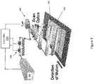
- FIG 3 illustrates an embodiment of a system for implementing a method of manufacturing the RF power package shown in Figures 1 and 2 .
- the system includes an energy source 200 such as a laser for patterning planar tuning lines in the metallized part 202 of a substrate 204.
- the system further includes a modulator 206 for modulating the energy output by the energy source 200, and in the case of a laser source, scan optics 208 for directing the modulated laser beam toward the metallized surface 202 of the substrate 204 being patterned.
- the substrate 204 can be a ceramic body with a metallized surface, a PCB panel with a laminated copper sheet, an eWLB-type carrier with a laminated foil, etc.
- the system also includes a controller 210 for controlling the energy source 200, modulator 206 and optics 208 (in the case of a laser source) so as to pattern the metallized part 202 of the substrate 204 into planar tuning lines.
- the system patterns a first plurality of planar tuning lines in the metallized part 202 of the substrate 204.
- the first plurality of planar tuning lines electrically connect the output terminal of an RF power transistor die to an output terminal of the package.
- the energy source 200, modulator 206 and optics 208 are controlled so as to shape the first plurality of planar tuning lines in a way such that the first plurality of planar tuning lines transforms the output impedance at the output terminal of the RF power transistor die to a higher target level at the package output terminal.
- the first plurality of planar tuning lines is shaped as straight lines because the first plurality of planar tuning lines will be on the output side of the RF power package.
- the first plurality of planar tuning lines can have a different shape if the target application warrants a different configuration for impedance matching/transformation.
- an output capacitor can be embedded in or subsequently attached to the substrate 204 after patterning.
- the output capacitor is electrically connected between the output terminal of the die and the package output terminal via the first plurality of planar tuning lines.
- the first plurality of planar tuning lines, as shaped by the system shown in Figure 3 , together with the output capacitor form an output impedance matching network as previously explained herein in connection with Figures 1 and 2 .
- the system controller 210 also controls the energy source 200, modulator 206 and optics 208 (in the case of a laser source) so as to pattern a second plurality of planar tuning lines in the metallized part 202 of the substrate 204.
- the second plurality of planar tuning lines electrically connect the input terminal of the RF power transistor to an input terminal of the RF power package via the second plurality of planar tuning lines.
- the second plurality of planar tuning lines is shaped by the system so as to transform the input impedance at the die input terminal to a different level at the package input terminal.
- An input capacitor can be embedded in or subsequently attached to the substrate 204 as previously explained herein.
- the input capacitor is electrically connected between the input terminal of the RF power transistor and the package input terminal via the second plurality of planar tuning lines.
- the second plurality of planar tuning lines as shaped by the system shown in Figure 3 , together with the input capacitor form an input impedance matching network.
- the second plurality of planar tuning lines can be shaped by the system as meandering lines so as transform the input impedance at the die input terminal to a different level at the package input terminal.
- the RF power transistor die and input and output capacitors are not shown in Figure 3 , and would be typically added to the RF power package after the metallized part 202 of the substrate 204 is patterned so as to form the planar tuning lines.
- the input and output capacitors may instead be embedded in the substrate 204, and therefore would be out of view in Figure 3 .
- both signal/power routing between packaging components and impedance matching/transformation are provided by appropriate patterning of the metallized part 202 of the substrate 204 into planar tuning lines.
- the system controller 210 can adjust its control of the energy source 200, modulator 206 and optics 208 (in the case of a laser source) to account for variations in the manufacturing process.
- the frequency response of RF matching networks is a complex function of geometry. As the width/spacing of the planar tuning lines varies during the manufacturing process, so too does the mutual impedance and loss of the planar tuning lines. Different line widths may need different correction factors.
- the thickness of the substrate 204 also effects the mutual impedance and loss of the planar tuning lines.
- Figure 4A illustrates part of a substrate 300 having a nominal thickness.
- Figure 4B illustrates the same part of another substrate 400 having a +10% variation in thickness.
- the mutual impedance and loss of the planar tuning lines 302 shown in Figure 4A differs from the mutual impedance and loss of the planar tuning lines 402 shown in Figure 4B due to the different substrate thicknesses.
- the system controller 210 can adjust its control of the energy source 200, modulator 206 and optics 208 (in the case of a laser source) so as to account for substrate thickness variation. Without this adaptation, the planar lines 302, 402 would have the same dimensions even though the substrate thicknesses are 10% different. As a result, the RF power packages will not have the same frequency response.
- Figure 5A illustrates the same substrate 300 shown in Figure 4A having a nominal thickness.
- Figure 5B illustrates the same part of another substrate 500 having a +10% variation in thickness.
- the system 210 accounts for the thicker substrate 500 when patterning the planar tuning lines 502 in the metallized part of the (thicker) substrate 500 shown in Figure 5B .
- the widths of the planar tuning lines 502 of the RF power package shown in Figure 5B are different than the widths of the planar tuning lines 302 of the RF power package shown in Figure 5A .
- the system controller 210 can also adjust its control of the energy source 200, modulator 206 and optics 208 (in the case of a laser source) to account for thinner than nominal package substrates. This way, RF power packages manufactured using the system described herein have approximately the same frequency response even though substrate thickness may vary, by applying different tuning patterns that account for variations in substrate thickness.
- the system controller 210 determines an initial shape of the planar tuning lines prior to formation based on a nominal thickness specified for the substrate.
- the planar tuning lines are then formed by determining the difference between the nominal thickness and a measured thickness of the substrate and determining, based on the difference between the nominal thickness and the measured thickness, an amount of adjustment needed to the initial shape so that the input and output impedances are still transformed to the corresponding target levels via the planar tuning lines when formed with the adjusted shape. This may involve widening, narrowing, lengthening, or shortening some or all of the planar tuning lines on the input and/or output side of the RF power package. Any standard approach such as visual inspection can be used for measuring the substrate thickness.
- the system controller 210 determines an initial shape of the planar tuning lines prior to formation based on an expected electrical parameter such as frequency response, impedance, etc. for the RF power transistor die. The system then forms the planar tuning lines by determining the difference between the expected electrical parameter and a corresponding measured electrical parameter of the RF power transistor die and determining, based on the difference between the expected electrical parameter and the measured electrical parameter, an amount of adjustment needed to the initial shape so that the input and output impedance of the RF power package is still transformed to the corresponding target levels via the planar tuning lines when formed with the adjusted shape. Any standard approach such as wafer level or die level testing can be used for measuring electrical parameters of the RF power transistor die.
- the system controller 210 can adjust its control of the energy source 200, modulator 206 and optics 208 (in the case of a laser source) to compensate for magnitude/phase/gain etc. variation.
- Figure 6A illustrates part of a Doherty amplifier package that includes main (M) and peaking (P) RF power transistor dies embedded in or attached to a substrate 600 and planar tuning lines formed in a metallized part of the substrate 600.
- the planar tuning lines are shaped so as to form output matching devices 602, 604 for both RF power transistor dies M, P and an impedance combiner such as a Doherty combiner.
- the Doherty combiner combines or sums the load currents of the amplifier dies M, P at a summing node so that the output voltage of the Doherty amplifier circuit is determined by the summation of the load currents multiplied by the load impedance.
- the Doherty combiner has a first impedance Z1 which couples the output of the main amplifier M to the summing node.
- the output of the peaking amplifier P is also coupled to the summing node.
- a second impedance Z2 of the Doherty combiner couples the summing node to the package output terminal 606.
- the first impedance Z1 of the Doherty combiner is implemented as a 1 ⁇ 4 wave transmission line 608 that phase aligns the signal outputs of the RF power transistor dies M, P such that the signal outputs are reactively combined at a first impedance level which is above the output impedance of the RF power transistor dies.
- the second impedance Z2 of the Doherty combiner is implemented as a 1 ⁇ 4 wave transmission line 610 that increases the impedance of the signal outputs to a second impedance level greater than the first impedance level at the package output terminal 606.
- planar tuning lines are formed in the metallized part of the substrate 600 for providing both signal/power routing and impedance matching/transformation on the input side of the Doherty amplifier package, but are not shown in Figures 6A and 6B for ease of illustration. These planar tuning lines can be shaped as needed e.g. as meandering lines so as to provide the desired impedance matching/transformation characteristic on the input side of the package.
- Figure 6B illustrates the same part of another Doherty amplifier package, but which has a substrate 700 with a +10% variation in thickness.
- the system controller 210 accounts for the thicker substrate when patterning the planar tuning lines in the metallized part of the (thicker) substrate 700 shown in Figure 6B .
- the widths of the planar tuning lines 702, 704, 708, 710 of the Doherty amplifier package shown in Figure 6B are different than the widths of the planar tuning lines 602, 604, 608, 610 of the Doherty amplifier package shown in Figure 6A .
- the system controller 210 also can adjust its control of the energy source 200, modulator 206 and optics 208 (in the case of a laser source) to account for thinner than nominal package substrates. This way, Doherty amplifier packages manufactured using the system described herein have approximately the same magnitude/phase/gain response even though substrate thickness may vary, by applying different tuning patterns that account for variations in substrate thickness.
Landscapes
- Engineering & Computer Science (AREA)
- Power Engineering (AREA)
- Microwave Amplifiers (AREA)
- Physics & Mathematics (AREA)
- Geometry (AREA)
- Ceramic Engineering (AREA)
- Manufacturing & Machinery (AREA)
Abstract
Description
- The present application relates to RF-power packages, more particularly to RF-power packages having tuning lines.
- Impedance matching is needed in RF power packages for moving the very low impedance of the power transistors to higher impedances so as to facilitate customer matching. Wire bonds are conventionally used for impedance matching/transformation, by changing impedances to different levels. Wire bonds are complex and expensive to implement, especially for tight tolerances required for low impedance matching. Wire bonding also requires special precise equipment and assembly procedures. It is difficult and costly to achieve and maintain consistent bonding and hence performance across many parts/wafers, and low-loss wire bond materials like gold are expensive. Hence, there is a need for an alternative impedance matching/transformation solution for RF power packages.
- According to an embodiment of an RF power package, the RF power package comprises a substrate having a metallized part and an insulating part, an RF power transistor die embedded in or attached to the substrate, the RF power transistor die having a die input terminal, a die output terminal, an input impedance and an output impedance, a package input terminal formed in the metallized part or attached to the insulating part of the substrate, a package output terminal formed in the metallized part or attached to the insulating part of the substrate, and a first plurality of planar tuning lines formed in the metallized part of the substrate and electrically connecting the die output terminal to the package output terminal. The first plurality of planar tuning lines is shaped so as to transform the output impedance at the die output terminal to a higher target level at the package output terminal.
- In some embodiments, the substrate comprises a ceramic body and a patterned metallization applied to the ceramic body, and wherein the patterned metallization forms the metallized part of the substrate.
- In some embodiments, the substrate is a printed circuit board comprising conductive tracks patterned into one or more copper sheets laminated onto a non-conductive body, and wherein the conductive tracks and the one or more copper sheets form the metallized part of the substrate.
- In some embodiments, the substrate comprises a first insulating material in which the RF power transistor die is embedded, a second insulating material covering the first insulating material and the RF power transistor die, and one or more metal redistribution layers disposed in the second insulating material, wherein each metal redistribution layer is electrically connected to die input terminal and/or die output terminal through openings in the second insulating material, and wherein the one or more metal redistribution layers form the metallized part of the substrate.
- In some embodiments, the first plurality of planar tuning lines is formed in straight lines.
- In some embodiments, the RF power package further comprises a capacitor embedded in or attached to the substrate and electrically connected between the die output terminal and the package output terminal, wherein the first plurality of planar tuning lines and the capacitor form an output impedance matching network.
- In some embodiments, the RF power package further comprises a second plurality of planar tuning lines formed in the metallized part of the substrate and electrically connecting the die input terminal to the package input terminal, wherein the second plurality of planar tuning lines is shaped so as to transform the input impedance at the die input terminal to a different level at the package input terminal.
- The RF power package of may further comprise a capacitor embedded in or attached to the substrate and electrically connected between the die input terminal and the package input terminal, wherein the second plurality of planar tuning lines and the second capacitor form an input impedance matching network.
- In some embodiments, the second plurality of planar tuning lines is formed in meandering lines.
- In some embodiments, the RF power package further comprises an additional RF power transistor die embedded in or attached to the substrate, the additional RF power transistor die having a die input terminal, a die output terminal, an input impedance and an output impedance, wherein the RF power transistor die is a main amplifier of a Doherty amplifier circuit, the additional RF power transistor die is a peaking amplifier of the Doherty amplifier circuit, and the first plurality of planar tuning lines is shaped so as to form a first % wave transmission line for phase aligning signal outputs of the RF power transistor dies such that the signal outputs are reactively combined at a first impedance level which is above the output impedance of the RF power transistor dies, and so as to form a second % wave transmission line for increasing the impedance of the signal outputs to a second impedance level greater than the first impedance level at the package output terminal.
- According to an embodiment of a method of manufacturing an RF power package, the method comprises: embedding or attaching an RF power transistor die to a substrate having a metallized part and an insulating part, the RF power transistor die having a die input terminal, a die output terminal, an input impedance and an output impedance; and forming a first plurality of planar tuning lines in the metallized part of the substrate, the first plurality of planar tuning lines electrically connecting the die output terminal to a package output terminal formed in the metallized part or attached to the insulating part of the substrate. The first plurality of planar tuning lines is formed by shaping the first plurality of planar tuning lines so that the first plurality of planar tuning lines transforms the output impedance at the die output terminal to a higher target level at the package output terminal.
- Shaping the first plurality of planar tuning lines so as to transform the output impedance at the die output terminal to the higher target level at the package output terminal may comprise shaping the first plurality of planar tuning lines as straight lines.
- The method may further comprise embedding or attaching a capacitor to the substrate; and electrically connecting the capacitor between the die output terminal and the package output terminal via the first plurality of planar tuning lines, wherein the first plurality of planar tuning lines and the capacitor form an output impedance matching network.
- The method may further comprise forming a second plurality of planar tuning lines in the metallized part of the substrate; and electrically connecting the die input terminal to a package input terminal formed in the metallized part or attached to the insulating part of the substrate via the second plurality of planar tuning lines, wherein the second plurality of planar tuning lines is shaped so as to transform the input impedance at the die input terminal to a different level at the package input terminal.
- The method may further comprise embedding or attaching a capacitor to the substrate; and electrically connecting the capacitor between the die input terminal and the package input terminal via the second plurality of planar tuning lines, wherein the second plurality of planar tuning lines and the second capacitor form an input impedance matching network.
- Shaping the second plurality of planar tuning lines so as transform the input impedance at the die input terminal to a different level at the package input terminal may comprise shaping the first plurality of planar tuning lines as meandering lines.
- In some embodiments, the method further comprises embedding or attaching an additional RF power transistor die to the substrate, the additional RF power transistor die having a die input terminal, a die output terminal, an input impedance and an output impedance, wherein the RF power transistor die is a main amplifier of a Doherty amplifier circuit, the additional RF power transistor die is a peaking amplifier of the Doherty amplifier circuit, and shaping the first plurality of planar tuning lines so as transform the output impedance at the die output terminal to the higher target level at the package output terminal comprises shaping the first plurality of planar tuning lines so as to form a first ¼ wave transmission line for phase aligning signal outputs of the RF power transistor dies such that the signal outputs are reactively combined at a first impedance level which is above the output impedance of the RF power transistor dies, and so as to form a second ¼ wave transmission line for increasing the impedance of the signal outputs to a second impedance level greater than the first impedance level at the package output terminal.
- In some embodiments, an initial shape of the first plurality of planar tuning lines is determined prior to formation based on a nominal thickness specified for the substrate, and wherein forming the first plurality of planar tuning lines comprises determining the difference between the nominal thickness and a measured thickness of the substrate; and determining, based on the difference between the nominal thickness and the measured thickness, an amount of adjustment needed to the initial shape so that the output impedance at the die output terminal is still transformed to the higher target level at the package output terminal via the first plurality of planar tuning lines when formed with the adjusted shape.
- In some embodiments, an initial shape of the first plurality of planar tuning lines is determined prior to formation based on an expected electrical parameter for the RF power transistor die, and wherein forming the first plurality of planar tuning lines comprises determining the difference between the expected electrical parameter and a measured electrical parameter of the RF power transistor die; and determining, based on the difference between the expected electrical parameter and the measured electrical parameter, an amount of adjustment needed to the initial shape so that the output impedance at the die output terminal is still transformed to the higher target level at the package output terminal via the first plurality of planar tuning lines when formed with the adjusted shape.
- Those skilled in the art will recognize additional features and advantages upon reading the following detailed description, and upon viewing the accompanying drawings.
- The elements of the drawings are not necessarily to scale relative to each other. Like reference numerals designate corresponding similar parts. The features of the various illustrated embodiments can be combined unless they exclude each other. Embodiments are depicted in the drawings and are detailed in the description which follows.
-
Figure 1 illustrates a top-down plan view an embodiment of an RF power package. -
Figure 2 illustrates a perspective view of the RF power package shown inFigure 1 . -
Figure 3 illustrates an embodiment of a system for manufacturing the RF power package shown inFigures 1 and2 . -
Figure 4A illustrates a top-down plan view of part of an RF power amplifier package having a substrate with nominal thickness. -
Figure 4B illustrates a top-down plan view of the same part of another RF power amplifier package having a substrate with +10% variation in thickness, without retuning. -
Figure 5A illustrates a top-down plan view of part of an RF power amplifier package having a substrate with nominal thickness. -
Figure 5B illustrates a top-down plan view of the same part of another RF power amplifier package having a substrate with +10% variation in thickness, with retuning. -
Figure 6A illustrates a top-down plan view of part of a Doherty amplifier package having a substrate with nominal thickness. -
Figure 6B illustrates a top-down plan view of the same part of another Doherty amplifier package having a substrate with +10% variation in thickness, with retuning. - Described next are embodiments of an RF power package in which conventional wire bond-based impedance matching/transformation e.g., for high-power transistors is replaced with planar tuning lines printed in the metallized part of a substrate (carrier). The impedance matching/transformation needed for a particular RF power package is optically defined, which is cheaper to implement and provides better consistency/accuracy compared to wire bonds. Optical line printing techniques are well established, thus eliminating the need for special precise wire bonding equipment and assembly procedures for implementing the desired impedance matching/transformation. Both signal/power routing between packaging components and the desired impedance matching/transformation are implemented by optically defined planar tuning lines.
-
Figure 1 illustrates a top-down plan view an embodiment of an RF power package, andFigure 2 illustrates a perspective view of the package. The RF power package comprises asubstrate 100 of length L and having ametallized part 102 and aninsulating part 104. At least one RF power transistor die 106 is embedded in or attached to thesubstrate 100. Each RF power transistor die 106 has a dieinput terminal 108, a dieoutput terminal 110, an input impedance and an output impedance. Apackage input terminal 112 and apackage output terminal 114 are formed in themetallized part 102 or attached to theinsulating part 104 of thesubstrate 100. A first plurality ofplanar tuning lines 116 are formed in themetallized part 102 of thesubstrate 100 and electrically connect thedie output terminal 110 to thepackage output terminal 114. The first plurality ofplanar tuning lines 116 is shaped so as to transform the output impedance at thedie output terminal 110 to a higher target level at thepackage output terminal 114. As such, the first plurality ofplanar tuning lines 116 provides both signal/power routing between packaging components and impedance matching/transformation. - The first plurality of
planar tuning lines 116 is shown inFigures 1 and2 as generally straight lines. This way, the impedance match/transformation on the output side of the RF power package is implemented using straight lines. Meandering lines can increase loss on the output side of the RF power package, but may be suitable in some applications. - SMT (surface mount technology) components such as capacitors, resistors, inductors, etc. can be included in the RF power package for direct in-package impedance matching/transformation.
Figures 1 and2 illustrate anoutput capacitor 118 embedded in or attached to thesubstrate 100 and electrically connected between thedie output terminal 110 and thepackage output terminal 114. The first plurality ofplanar tuning lines 116 and theoutput capacitor 118 form an output impedance matching network of the RF power package. - A second plurality of
planar tuning lines 120 formed in themetallized part 102 of thesubstrate 100 electrically connect thedie input terminal 108 to thepackage input terminal 112. The second plurality ofplanar tuning lines 120 is shaped so as to transform the input impedance at thedie input terminal 108 to a different level at thepackage input terminal 112. Aninput capacitor 122 embedded in or attached to thesubstrate 100 is electrically connected between thedie input terminal 108 and thepackage input terminal 112. The second plurality ofplanar tuning lines 120 and theinput capacitor 122 form an input impedance matching network of the RF power package. In one embodiment, the second plurality ofplanar tuning lines 120 is formed in meandering lines so as to provide the desired impedance matching/transformation on the input side of the RF power package. - The RF power package design shown in
Figures 1 and2 obviates the need for bond wires of different lengths and heights on the input and output sides of the package. Instead, the desired impedance matching/transformation on the input and output sides of the package is provided by the planar meandering tuninglines - The RF power package design shown in
Figures 1 and2 , in which both signal/power routing and impedance matching/transformation are provided by optically definedplanar tuning lines planar tuning lines planar tuning lines - The RF power package configuration can also be used to implement Doherty RF power packages, in which more than one RF power amplifier die is included in the package and the desired impedance matching/transformation and even possibly the Doherty combining network can be implemented using the optically defined printed
planar lines - In one embodiment, the
substrate 100 of the RF power package comprises a ceramic body and a patterned metallization applied to the ceramic body. The patterned metallization forms themetallized part 102 of thesubstrate 100 according to this embodiment. For example, the substrate can be a DCB (direct copper bonded) substrate, an AMB (active metal brazed) substrate, a DAB (direct aluminum bonded) substrate, etc. - In another embodiment, the
substrate 100 is a printed circuit board (PCB). The PCB has conductive tracks / microstrips / traces patterned into one or more copper sheets laminated onto a non-conductive body. The conductive tracks and the one or more copper sheets form themetallized part 102 of thesubstrate 100 according to this embodiment. - In yet another embodiment, the
substrate 100 is an eWLB (embedded wafer level ball grid array) type substrate that comprises a first insulating material in which the RF power transistor die 106 is embedded, a second insulating material covering the first insulating material and the RF power transistor die 106, and one or more metal redistribution layers disposed in the second insulating material. Each metal redistribution layer is electrically connected to dieinput terminal 108 and/or dieoutput terminal 110 through openings in the second insulating material. The one or more metal redistribution layers form themetallized part 102 of thesubstrate 100 according to this embodiment. -
Figure 3 illustrates an embodiment of a system for implementing a method of manufacturing the RF power package shown inFigures 1 and2 . The system includes anenergy source 200 such as a laser for patterning planar tuning lines in themetallized part 202 of asubstrate 204. The system further includes amodulator 206 for modulating the energy output by theenergy source 200, and in the case of a laser source, scanoptics 208 for directing the modulated laser beam toward the metallizedsurface 202 of thesubstrate 204 being patterned. As previously explained herein, thesubstrate 204 can be a ceramic body with a metallized surface, a PCB panel with a laminated copper sheet, an eWLB-type carrier with a laminated foil, etc. - The system also includes a
controller 210 for controlling theenergy source 200,modulator 206 and optics 208 (in the case of a laser source) so as to pattern themetallized part 202 of thesubstrate 204 into planar tuning lines. For the RF power package shown inFigures 1 and2 , the system patterns a first plurality of planar tuning lines in themetallized part 202 of thesubstrate 204. The first plurality of planar tuning lines electrically connect the output terminal of an RF power transistor die to an output terminal of the package. Theenergy source 200,modulator 206 and optics 208 (in the case of a laser source) are controlled so as to shape the first plurality of planar tuning lines in a way such that the first plurality of planar tuning lines transforms the output impedance at the output terminal of the RF power transistor die to a higher target level at the package output terminal. In one embodiment, the first plurality of planar tuning lines is shaped as straight lines because the first plurality of planar tuning lines will be on the output side of the RF power package. However, the first plurality of planar tuning lines can have a different shape if the target application warrants a different configuration for impedance matching/transformation. - As previously explained herein, an output capacitor can be embedded in or subsequently attached to the
substrate 204 after patterning. The output capacitor is electrically connected between the output terminal of the die and the package output terminal via the first plurality of planar tuning lines. The first plurality of planar tuning lines, as shaped by the system shown inFigure 3 , together with the output capacitor form an output impedance matching network as previously explained herein in connection withFigures 1 and2 . - The
system controller 210 also controls theenergy source 200,modulator 206 and optics 208 (in the case of a laser source) so as to pattern a second plurality of planar tuning lines in themetallized part 202 of thesubstrate 204. The second plurality of planar tuning lines electrically connect the input terminal of the RF power transistor to an input terminal of the RF power package via the second plurality of planar tuning lines. The second plurality of planar tuning lines is shaped by the system so as to transform the input impedance at the die input terminal to a different level at the package input terminal. An input capacitor can be embedded in or subsequently attached to thesubstrate 204 as previously explained herein. The input capacitor is electrically connected between the input terminal of the RF power transistor and the package input terminal via the second plurality of planar tuning lines. The second plurality of planar tuning lines, as shaped by the system shown inFigure 3 , together with the input capacitor form an input impedance matching network. The second plurality of planar tuning lines can be shaped by the system as meandering lines so as transform the input impedance at the die input terminal to a different level at the package input terminal. - The RF power transistor die and input and output capacitors are not shown in
Figure 3 , and would be typically added to the RF power package after themetallized part 202 of thesubstrate 204 is patterned so as to form the planar tuning lines. The input and output capacitors may instead be embedded in thesubstrate 204, and therefore would be out of view inFigure 3 . In each case, both signal/power routing between packaging components and impedance matching/transformation are provided by appropriate patterning of themetallized part 202 of thesubstrate 204 into planar tuning lines. - The
system controller 210 can adjust its control of theenergy source 200,modulator 206 and optics 208 (in the case of a laser source) to account for variations in the manufacturing process. The frequency response of RF matching networks is a complex function of geometry. As the width/spacing of the planar tuning lines varies during the manufacturing process, so too does the mutual impedance and loss of the planar tuning lines. Different line widths may need different correction factors. The thickness of thesubstrate 204 also effects the mutual impedance and loss of the planar tuning lines. -
Figure 4A illustrates part of asubstrate 300 having a nominal thickness.Figure 4B illustrates the same part of anothersubstrate 400 having a +10% variation in thickness. The mutual impedance and loss of theplanar tuning lines 302 shown inFigure 4A differs from the mutual impedance and loss of theplanar tuning lines 402 shown inFigure 4B due to the different substrate thicknesses. Thesystem controller 210 can adjust its control of theenergy source 200,modulator 206 and optics 208 (in the case of a laser source) so as to account for substrate thickness variation. Without this adaptation, theplanar lines -
Figure 5A illustrates thesame substrate 300 shown inFigure 4A having a nominal thickness.Figure 5B illustrates the same part of anothersubstrate 500 having a +10% variation in thickness. Different than thesubstrate 400 shown inFigure 4B , thesystem 210 accounts for thethicker substrate 500 when patterning theplanar tuning lines 502 in the metallized part of the (thicker)substrate 500 shown inFigure 5B . The widths of theplanar tuning lines 502 of the RF power package shown inFigure 5B are different than the widths of theplanar tuning lines 302 of the RF power package shown inFigure 5A . Thesystem controller 210 can also adjust its control of theenergy source 200,modulator 206 and optics 208 (in the case of a laser source) to account for thinner than nominal package substrates. This way, RF power packages manufactured using the system described herein have approximately the same frequency response even though substrate thickness may vary, by applying different tuning patterns that account for variations in substrate thickness. - In one embodiment, the
system controller 210 determines an initial shape of the planar tuning lines prior to formation based on a nominal thickness specified for the substrate. The planar tuning lines are then formed by determining the difference between the nominal thickness and a measured thickness of the substrate and determining, based on the difference between the nominal thickness and the measured thickness, an amount of adjustment needed to the initial shape so that the input and output impedances are still transformed to the corresponding target levels via the planar tuning lines when formed with the adjusted shape. This may involve widening, narrowing, lengthening, or shortening some or all of the planar tuning lines on the input and/or output side of the RF power package. Any standard approach such as visual inspection can be used for measuring the substrate thickness. - In another embodiment, the
system controller 210 determines an initial shape of the planar tuning lines prior to formation based on an expected electrical parameter such as frequency response, impedance, etc. for the RF power transistor die. The system then forms the planar tuning lines by determining the difference between the expected electrical parameter and a corresponding measured electrical parameter of the RF power transistor die and determining, based on the difference between the expected electrical parameter and the measured electrical parameter, an amount of adjustment needed to the initial shape so that the input and output impedance of the RF power package is still transformed to the corresponding target levels via the planar tuning lines when formed with the adjusted shape. Any standard approach such as wafer level or die level testing can be used for measuring electrical parameters of the RF power transistor die. - In the case of Doherty power amplifiers, the
system controller 210 can adjust its control of theenergy source 200,modulator 206 and optics 208 (in the case of a laser source) to compensate for magnitude/phase/gain etc. variation. -
Figure 6A illustrates part of a Doherty amplifier package that includes main (M) and peaking (P) RF power transistor dies embedded in or attached to asubstrate 600 and planar tuning lines formed in a metallized part of thesubstrate 600. The planar tuning lines are shaped so as to formoutput matching devices package output terminal 606. The first impedance Z1 of the Doherty combiner is implemented as a ¼wave transmission line 608 that phase aligns the signal outputs of the RF power transistor dies M, P such that the signal outputs are reactively combined at a first impedance level which is above the output impedance of the RF power transistor dies. The second impedance Z2 of the Doherty combiner is implemented as a ¼wave transmission line 610 that increases the impedance of the signal outputs to a second impedance level greater than the first impedance level at thepackage output terminal 606. - Additional planar tuning lines are formed in the metallized part of the
substrate 600 for providing both signal/power routing and impedance matching/transformation on the input side of the Doherty amplifier package, but are not shown inFigures 6A and 6B for ease of illustration. These planar tuning lines can be shaped as needed e.g. as meandering lines so as to provide the desired impedance matching/transformation characteristic on the input side of the package. -
Figure 6B illustrates the same part of another Doherty amplifier package, but which has asubstrate 700 with a +10% variation in thickness. Thesystem controller 210 accounts for the thicker substrate when patterning the planar tuning lines in the metallized part of the (thicker)substrate 700 shown inFigure 6B . As a result, the widths of theplanar tuning lines Figure 6B are different than the widths of theplanar tuning lines Figure 6A . Thesystem controller 210 also can adjust its control of theenergy source 200,modulator 206 and optics 208 (in the case of a laser source) to account for thinner than nominal package substrates. This way, Doherty amplifier packages manufactured using the system described herein have approximately the same magnitude/phase/gain response even though substrate thickness may vary, by applying different tuning patterns that account for variations in substrate thickness. - Spatially relative terms such as "under", "below", "lower", "over", "upper" and the like, are used for ease of description to explain the positioning of one element relative to a second element. These terms are intended to encompass different orientations of the device in addition to different orientations than those depicted in the figures. Further, terms such as "first", "second", and the like, are also used to describe various elements, regions, sections, etc. and are also not intended to be limiting. Like terms refer to like elements throughout the description.
- As used herein, the terms "having", "containing", "including", "comprising" and the like are open ended terms that indicate the presence of stated elements or features, but do not preclude additional elements or features. The articles "a", "an" and "the" are intended to include the plural as well as the singular, unless the context clearly indicates otherwise.
- It is to be understood that the features of the various embodiments described herein may be combined with each other, unless specifically noted otherwise.
- Although specific embodiments have been illustrated and described herein, it will be appreciated by those of ordinary skill in the art that a variety of alternate and/or equivalent implementations may be substituted for the specific embodiments shown and described without departing from the scope of the present invention. This application is intended to cover any adaptations or variations of the specific embodiments discussed herein. Therefore, it is intended that this invention be limited only by the claims and the equivalents thereof.
Claims (15)
- An RF power package, comprising:a substrate having a metallized part and an insulating part;an RF power transistor die embedded in or attached to the substrate, the RF power transistor die having a die input terminal, a die output terminal, an input impedance and an output impedance;a package input terminal formed in the metallized part or attached to the insulating part of the substrate;a package output terminal formed in the metallized part or attached to the insulating part of the substrate; anda first plurality of planar tuning lines formed in the metallized part of the substrate and electrically connecting the die output terminal to the package output terminal,wherein the first plurality of planar tuning lines is shaped so as to transform the output impedance at the die output terminal to a higher target level at the package output terminal.
- The RF power package of claim 1, wherein the substrate comprises a ceramic body and a patterned metallization applied to the ceramic body, and wherein the patterned metallization forms the metallized part of the substrate, or the substrate is a printed circuit board comprising conductive tracks patterned into one or more copper sheets laminated onto a non-conductive body, and wherein the conductive tracks and the one or more copper sheets form the metallized part of the substrate, or the substrate comprises a first insulating material in which the RF power transistor die is embedded, a second insulating material covering the first insulating material and the RF power transistor die, and one or more metal redistribution layers disposed in the second insulating material, wherein each metal redistribution layer is electrically connected to die input terminal and/or die output terminal through openings in the second insulating material, and wherein the one or more metal redistribution layers form the metallized part of the substrate.
- The RF power package of claim 1 or claim 2, wherein the first plurality of planar tuning lines is formed in straight lines.
- The RF power package of any one of claims 1 to 3, further comprising:a capacitor embedded in or attached to the substrate and electrically connected between the die output terminal and the package output terminal,wherein the first plurality of planar tuning lines and the capacitor form an output impedance matching network.
- The RF power package of any one of claims 1 to 4, further comprising:a second plurality of planar tuning lines formed in the metallized part of the substrate and electrically connecting the die input terminal to the package input terminal,wherein the second plurality of planar tuning lines is shaped so as to transform the input impedance at the die input terminal to a different level at the package input terminal.
- The RF power package of claim 5, further comprising:a capacitor embedded in or attached to the substrate and electrically connected between the die input terminal and the package input terminal,wherein the second plurality of planar tuning lines and the second capacitor form an input impedance matching network.
- The RF power package of claim 5 or claim 6, wherein the second plurality of planar tuning lines is formed in meandering lines.
- The RF power package of any one of claims 1 to 7, further comprising:an additional RF power transistor die embedded in or attached to the substrate, the additional RF power transistor die having a die input terminal, a die output terminal, an input impedance and an output impedance,wherein the RF power transistor die is a main amplifier of a Doherty amplifier circuit,wherein the additional RF power transistor die is a peaking amplifier of the Doherty amplifier circuit,wherein the first plurality of planar tuning lines is shaped so as to form a first % wave transmission line for phase aligning signal outputs of the RF power transistor dies such that the signal outputs are reactively combined at a first impedance level which is above the output impedance of the RF power transistor dies, and so as to form a second ¼ wave transmission line for increasing the impedance of the signal outputs to a second impedance level greater than the first impedance level at the package output terminal.
- A method of manufacturing an RF power package, the method comprising:embedding or attaching an RF power transistor die to a substrate having a metallized part and an insulating part, the RF power transistor die having a die input terminal, a die output terminal, an input impedance and an output impedance; andforming a first plurality of planar tuning lines in the metallized part of the substrate, the first plurality of planar tuning lines electrically connecting the die output terminal to a package output terminal formed in the metallized part or attached to the insulating part of the substrate,wherein forming the first plurality of planar tuning lines comprises shaping the first plurality of planar tuning lines so that the first plurality of planar tuning lines transforms the output impedance at the die output terminal to a higher target level at the package output terminal.
- The method of claim 9, wherein shaping the first plurality of planar tuning lines so as to transform the output impedance at the die output terminal to the higher target level at the package output terminal comprises shaping the first plurality of planar tuning lines as straight lines.
- The method of claim 9 or claim 10, further comprising:embedding or attaching a capacitor to the substrate; andelectrically connecting the capacitor between the die output terminal and the package output terminal via the first plurality of planar tuning lines,wherein the first plurality of planar tuning lines and the capacitor form an output impedance matching network.
- The method of any one of claims 9 to 11, further comprising:forming a second plurality of planar tuning lines in the metallized part of the substrate; andelectrically connecting the die input terminal to a package input terminal formed in the metallized part or attached to the insulating part of the substrate via the second plurality of planar tuning lines,wherein the second plurality of planar tuning lines is shaped so as to transform the input impedance at the die input terminal to a different level at the package input terminal, and optionally further comprising:embedding or attaching a capacitor to the substrate; andelectrically connecting the capacitor between the die input terminal and the package input terminal via the second plurality of planar tuning lines,wherein the second plurality of planar tuning lines and the second capacitor form an input impedance matching network.
- The method of claim 12, wherein shaping the second plurality of planar tuning lines so as transform the input impedance at the die input terminal to a different level at the package input terminal comprises shaping the first plurality of planar tuning lines as meandering lines.
- The method of any one of claims 9 to 13, further comprising:embedding or attaching an additional RF power transistor die to the substrate, the additional RF power transistor die having a die input terminal, a die output terminal, an input impedance and an output impedance,wherein the RF power transistor die is a main amplifier of a Doherty amplifier circuit,wherein the additional RF power transistor die is a peaking amplifier of the Doherty amplifier circuit,wherein shaping the first plurality of planar tuning lines so as transform the output impedance at the die output terminal to the higher target level at the package output terminal comprises shaping the first plurality of planar tuning lines so as to form a first % wave transmission line for phase aligning signal outputs of the RF power transistor dies such that the signal outputs are reactively combined at a first impedance level which is above the output impedance of the RF power transistor dies, and so as to form a second ¼ wave transmission line for increasing the impedance of the signal outputs to a second impedance level greater than the first impedance level at the package output terminal.
- The method of any one of claims 9 to 14, wherein an initial shape of the first plurality of planar tuning lines is determined prior to formation based on a nominal thickness specified for the substrate, and wherein forming the first plurality of planar tuning lines comprises:determining the difference between the nominal thickness and a measured thickness of the substrate; anddetermining, based on the difference between the nominal thickness and the measured thickness, an amount of adjustment needed to the initial shape so that the output impedance at the die output terminal is still transformed to the higher target level at the package output terminal via the first plurality of planar tuning lines when formed with the adjusted shape, and/or an initial shape of the first plurality of planar tuning lines is determined prior to formation based on an expected electrical parameter for the RF power transistor die, and wherein forming the first plurality of planar tuning lines comprises:determining the difference between the expected electrical parameter and a measured electrical parameter of the RF power transistor die; anddetermining, based on the difference between the expected electrical parameter and the measured electrical parameter, an amount of adjustment needed to the initial shape so that the output impedance at the die output terminal is still transformed to the higher target level at the package output terminal via the first plurality of planar tuning lines when formed with the adjusted shape.
Applications Claiming Priority (1)
| Application Number | Priority Date | Filing Date | Title |
|---|---|---|---|
| US15/355,498 US10978411B2 (en) | 2016-11-18 | 2016-11-18 | RF power package having planar tuning lines |
Publications (2)
| Publication Number | Publication Date |
|---|---|
| EP3324433A1 true EP3324433A1 (en) | 2018-05-23 |
| EP3324433B1 EP3324433B1 (en) | 2021-01-06 |
Family
ID=60327173
Family Applications (1)
| Application Number | Title | Priority Date | Filing Date |
|---|---|---|---|
| EP17201709.7A Active EP3324433B1 (en) | 2016-11-18 | 2017-11-14 | Rf power package having planar tuning lines |
Country Status (3)
| Country | Link |
|---|---|
| US (1) | US10978411B2 (en) |
| EP (1) | EP3324433B1 (en) |
| CN (1) | CN108074915B (en) |
Citations (3)
| Publication number | Priority date | Publication date | Assignee | Title |
|---|---|---|---|---|
| US20120025915A1 (en) * | 2010-07-27 | 2012-02-02 | Sumitomo Electric Device Innovations, Inc. | Doherty amplifier |
| US9065391B1 (en) * | 2012-09-17 | 2015-06-23 | Bae Systems Information And Electronic Systems Integration Inc. | Method of operating a power amplifier in class F/inverse class F |
| US20160294340A1 (en) * | 2015-03-31 | 2016-10-06 | Infineon Technologies Ag | Multi-cavity package having single metal flange |
Family Cites Families (8)
| Publication number | Priority date | Publication date | Assignee | Title |
|---|---|---|---|---|
| DE69123626T2 (en) * | 1990-04-16 | 1997-04-17 | Fujitsu Ltd | Chip carriers for fabricating a high power microwave semiconductor device by placing a semiconductor chip thereon |
| JP2883218B2 (en) * | 1991-03-27 | 1999-04-19 | 三菱電機株式会社 | Semiconductor amplifier |
| US5446961A (en) | 1993-10-15 | 1995-09-05 | International Business Machines Corporation | Method for repairing semiconductor substrates |
| FI106414B (en) * | 1999-02-02 | 2001-01-31 | Nokia Networks Oy | Bredbandsimpedansadapter |
| US6462423B1 (en) | 2000-08-31 | 2002-10-08 | Micron Technology, Inc. | Flip-chip with matched lines and ground plane |
| EP2339746B1 (en) | 2009-12-15 | 2013-02-20 | Nxp B.V. | Doherty amplifier with composed transfer characteristic having multiple peak amplifiers |
| JP2012156362A (en) * | 2011-01-27 | 2012-08-16 | Fujitsu Ltd | Transmission line, integrated circuit mounting device and communication module |
| US9787254B2 (en) * | 2015-09-23 | 2017-10-10 | Nxp Usa, Inc. | Encapsulated semiconductor device package with heatsink opening, and methods of manufacture thereof |
-
2016
- 2016-11-18 US US15/355,498 patent/US10978411B2/en active Active
-
2017
- 2017-11-14 EP EP17201709.7A patent/EP3324433B1/en active Active
- 2017-11-20 CN CN201711160463.4A patent/CN108074915B/en active Active
Patent Citations (3)
| Publication number | Priority date | Publication date | Assignee | Title |
|---|---|---|---|---|
| US20120025915A1 (en) * | 2010-07-27 | 2012-02-02 | Sumitomo Electric Device Innovations, Inc. | Doherty amplifier |
| US9065391B1 (en) * | 2012-09-17 | 2015-06-23 | Bae Systems Information And Electronic Systems Integration Inc. | Method of operating a power amplifier in class F/inverse class F |
| US20160294340A1 (en) * | 2015-03-31 | 2016-10-06 | Infineon Technologies Ag | Multi-cavity package having single metal flange |
Also Published As
| Publication number | Publication date |
|---|---|
| CN108074915A (en) | 2018-05-25 |
| US20180145043A1 (en) | 2018-05-24 |
| US10978411B2 (en) | 2021-04-13 |
| CN108074915B (en) | 2021-03-09 |
| EP3324433B1 (en) | 2021-01-06 |
Similar Documents
| Publication | Publication Date | Title |
|---|---|---|
| US20220352141A1 (en) | Multi-Cavity Package Having Single Metal Flange | |
| US9450547B2 (en) | Semiconductor package having an isolation wall to reduce electromagnetic coupling | |
| JP7103561B2 (en) | Semiconductor equipment | |
| US8558638B2 (en) | Impedance transformer, integrated circuit device, amplifier, and communicator module | |
| EP3211669B1 (en) | Semiconductor package with isolation wall | |
| US10109594B2 (en) | Semiconductor device with an isolation structure coupled to a cover of the semiconductor device | |
| US20160322942A1 (en) | Improved matching techniques for wide-bandgap power transistors | |
| EP3324433B1 (en) | Rf power package having planar tuning lines | |
| US6661101B2 (en) | Semiconductor device | |
| CN112737515B (en) | DOHERTY amplifier device | |
| US6399894B1 (en) | Wire bond compensation | |
| US11303254B2 (en) | Amplifier | |
| JP6557561B2 (en) | High frequency semiconductor device | |
| JP7371340B2 (en) | Power amplification equipment and electromagnetic radiation equipment | |
| JP2017055224A (en) | High frequency semiconductor device | |
| JP6527429B2 (en) | High frequency semiconductor device | |
| JP2012089935A (en) | High frequency module connection structure | |
| WO2021171671A1 (en) | Ic module and method for manufacturing ic module | |
| WO2019107183A1 (en) | Wiring board and method for manufacturing wiring board | |
| JP2000269383A (en) | Mounting structure and mounting method of high frequency circuit element |
Legal Events
| Date | Code | Title | Description |
|---|---|---|---|
| PUAI | Public reference made under article 153(3) epc to a published international application that has entered the european phase |
Free format text: ORIGINAL CODE: 0009012 |
|
| STAA | Information on the status of an ep patent application or granted ep patent |
Free format text: STATUS: THE APPLICATION HAS BEEN PUBLISHED |
|
| AK | Designated contracting states |
Kind code of ref document: A1 Designated state(s): AL AT BE BG CH CY CZ DE DK EE ES FI FR GB GR HR HU IE IS IT LI LT LU LV MC MK MT NL NO PL PT RO RS SE SI SK SM TR |
|
| AX | Request for extension of the european patent |
Extension state: BA ME |
|
| STAA | Information on the status of an ep patent application or granted ep patent |
Free format text: STATUS: REQUEST FOR EXAMINATION WAS MADE |
|
| 17P | Request for examination filed |
Effective date: 20181123 |
|
| RBV | Designated contracting states (corrected) |
Designated state(s): AL AT BE BG CH CY CZ DE DK EE ES FI FR GB GR HR HU IE IS IT LI LT LU LV MC MK MT NL NO PL PT RO RS SE SI SK SM TR |
|
| GRAP | Despatch of communication of intention to grant a patent |
Free format text: ORIGINAL CODE: EPIDOSNIGR1 |
|
| STAA | Information on the status of an ep patent application or granted ep patent |
Free format text: STATUS: GRANT OF PATENT IS INTENDED |
|
| RIC1 | Information provided on ipc code assigned before grant |
Ipc: H01L 23/48 20060101ALI20200706BHEP Ipc: H01L 23/485 20060101AFI20200706BHEP Ipc: H03F 3/60 20060101ALI20200706BHEP Ipc: H01L 23/538 20060101ALI20200706BHEP Ipc: H01L 25/07 20060101ALI20200706BHEP Ipc: H01L 21/66 20060101ALI20200706BHEP Ipc: H03H 7/38 20060101ALI20200706BHEP Ipc: H01P 5/02 20060101ALI20200706BHEP Ipc: H03F 1/02 20060101ALI20200706BHEP Ipc: H01L 23/00 20060101ALI20200706BHEP Ipc: H01L 23/66 20060101ALI20200706BHEP |
|
| INTG | Intention to grant announced |
Effective date: 20200727 |
|
| GRAS | Grant fee paid |
Free format text: ORIGINAL CODE: EPIDOSNIGR3 |
|
| GRAA | (expected) grant |
Free format text: ORIGINAL CODE: 0009210 |
|
| STAA | Information on the status of an ep patent application or granted ep patent |
Free format text: STATUS: THE PATENT HAS BEEN GRANTED |
|
| AK | Designated contracting states |
Kind code of ref document: B1 Designated state(s): AL AT BE BG CH CY CZ DE DK EE ES FI FR GB GR HR HU IE IS IT LI LT LU LV MC MK MT NL NO PL PT RO RS SE SI SK SM TR |
|
| REG | Reference to a national code |
Ref country code: GB Ref legal event code: FG4D |
|
| REG | Reference to a national code |
Ref country code: AT Ref legal event code: REF Ref document number: 1353290 Country of ref document: AT Kind code of ref document: T Effective date: 20210115 Ref country code: CH Ref legal event code: EP |
|
| REG | Reference to a national code |
Ref country code: DE Ref legal event code: R096 Ref document number: 602017030841 Country of ref document: DE |
|
| REG | Reference to a national code |
Ref country code: IE Ref legal event code: FG4D |
|
| REG | Reference to a national code |
Ref country code: NL Ref legal event code: MP Effective date: 20210106 |
|
| REG | Reference to a national code |
Ref country code: AT Ref legal event code: MK05 Ref document number: 1353290 Country of ref document: AT Kind code of ref document: T Effective date: 20210106 |
|
| REG | Reference to a national code |
Ref country code: LT Ref legal event code: MG9D |
|
| PG25 | Lapsed in a contracting state [announced via postgrant information from national office to epo] |
Ref country code: PT Free format text: LAPSE BECAUSE OF FAILURE TO SUBMIT A TRANSLATION OF THE DESCRIPTION OR TO PAY THE FEE WITHIN THE PRESCRIBED TIME-LIMIT Effective date: 20210506 Ref country code: NO Free format text: LAPSE BECAUSE OF FAILURE TO SUBMIT A TRANSLATION OF THE DESCRIPTION OR TO PAY THE FEE WITHIN THE PRESCRIBED TIME-LIMIT Effective date: 20210406 Ref country code: FI Free format text: LAPSE BECAUSE OF FAILURE TO SUBMIT A TRANSLATION OF THE DESCRIPTION OR TO PAY THE FEE WITHIN THE PRESCRIBED TIME-LIMIT Effective date: 20210106 Ref country code: HR Free format text: LAPSE BECAUSE OF FAILURE TO SUBMIT A TRANSLATION OF THE DESCRIPTION OR TO PAY THE FEE WITHIN THE PRESCRIBED TIME-LIMIT Effective date: 20210106 Ref country code: GR Free format text: LAPSE BECAUSE OF FAILURE TO SUBMIT A TRANSLATION OF THE DESCRIPTION OR TO PAY THE FEE WITHIN THE PRESCRIBED TIME-LIMIT Effective date: 20210407 Ref country code: BG Free format text: LAPSE BECAUSE OF FAILURE TO SUBMIT A TRANSLATION OF THE DESCRIPTION OR TO PAY THE FEE WITHIN THE PRESCRIBED TIME-LIMIT Effective date: 20210406 Ref country code: LT Free format text: LAPSE BECAUSE OF FAILURE TO SUBMIT A TRANSLATION OF THE DESCRIPTION OR TO PAY THE FEE WITHIN THE PRESCRIBED TIME-LIMIT Effective date: 20210106 |
|
| PG25 | Lapsed in a contracting state [announced via postgrant information from national office to epo] |
Ref country code: SE Free format text: LAPSE BECAUSE OF FAILURE TO SUBMIT A TRANSLATION OF THE DESCRIPTION OR TO PAY THE FEE WITHIN THE PRESCRIBED TIME-LIMIT Effective date: 20210106 Ref country code: RS Free format text: LAPSE BECAUSE OF FAILURE TO SUBMIT A TRANSLATION OF THE DESCRIPTION OR TO PAY THE FEE WITHIN THE PRESCRIBED TIME-LIMIT Effective date: 20210106 Ref country code: LV Free format text: LAPSE BECAUSE OF FAILURE TO SUBMIT A TRANSLATION OF THE DESCRIPTION OR TO PAY THE FEE WITHIN THE PRESCRIBED TIME-LIMIT Effective date: 20210106 Ref country code: PL Free format text: LAPSE BECAUSE OF FAILURE TO SUBMIT A TRANSLATION OF THE DESCRIPTION OR TO PAY THE FEE WITHIN THE PRESCRIBED TIME-LIMIT Effective date: 20210106 Ref country code: AT Free format text: LAPSE BECAUSE OF FAILURE TO SUBMIT A TRANSLATION OF THE DESCRIPTION OR TO PAY THE FEE WITHIN THE PRESCRIBED TIME-LIMIT Effective date: 20210106 |
|
| PG25 | Lapsed in a contracting state [announced via postgrant information from national office to epo] |
Ref country code: IS Free format text: LAPSE BECAUSE OF FAILURE TO SUBMIT A TRANSLATION OF THE DESCRIPTION OR TO PAY THE FEE WITHIN THE PRESCRIBED TIME-LIMIT Effective date: 20210506 |
|
| REG | Reference to a national code |
Ref country code: DE Ref legal event code: R097 Ref document number: 602017030841 Country of ref document: DE |
|
| PG25 | Lapsed in a contracting state [announced via postgrant information from national office to epo] |
Ref country code: CZ Free format text: LAPSE BECAUSE OF FAILURE TO SUBMIT A TRANSLATION OF THE DESCRIPTION OR TO PAY THE FEE WITHIN THE PRESCRIBED TIME-LIMIT Effective date: 20210106 Ref country code: EE Free format text: LAPSE BECAUSE OF FAILURE TO SUBMIT A TRANSLATION OF THE DESCRIPTION OR TO PAY THE FEE WITHIN THE PRESCRIBED TIME-LIMIT Effective date: 20210106 Ref country code: SM Free format text: LAPSE BECAUSE OF FAILURE TO SUBMIT A TRANSLATION OF THE DESCRIPTION OR TO PAY THE FEE WITHIN THE PRESCRIBED TIME-LIMIT Effective date: 20210106 |
|
| PLBE | No opposition filed within time limit |
Free format text: ORIGINAL CODE: 0009261 |
|
| STAA | Information on the status of an ep patent application or granted ep patent |
Free format text: STATUS: NO OPPOSITION FILED WITHIN TIME LIMIT |
|
| PG25 | Lapsed in a contracting state [announced via postgrant information from national office to epo] |
Ref country code: DK Free format text: LAPSE BECAUSE OF FAILURE TO SUBMIT A TRANSLATION OF THE DESCRIPTION OR TO PAY THE FEE WITHIN THE PRESCRIBED TIME-LIMIT Effective date: 20210106 Ref country code: RO Free format text: LAPSE BECAUSE OF FAILURE TO SUBMIT A TRANSLATION OF THE DESCRIPTION OR TO PAY THE FEE WITHIN THE PRESCRIBED TIME-LIMIT Effective date: 20210106 Ref country code: SK Free format text: LAPSE BECAUSE OF FAILURE TO SUBMIT A TRANSLATION OF THE DESCRIPTION OR TO PAY THE FEE WITHIN THE PRESCRIBED TIME-LIMIT Effective date: 20210106 |
|
| 26N | No opposition filed |
Effective date: 20211007 |
|
| PG25 | Lapsed in a contracting state [announced via postgrant information from national office to epo] |
Ref country code: ES Free format text: LAPSE BECAUSE OF FAILURE TO SUBMIT A TRANSLATION OF THE DESCRIPTION OR TO PAY THE FEE WITHIN THE PRESCRIBED TIME-LIMIT Effective date: 20210106 Ref country code: AL Free format text: LAPSE BECAUSE OF FAILURE TO SUBMIT A TRANSLATION OF THE DESCRIPTION OR TO PAY THE FEE WITHIN THE PRESCRIBED TIME-LIMIT Effective date: 20210106 |
|
| PG25 | Lapsed in a contracting state [announced via postgrant information from national office to epo] |
Ref country code: SI Free format text: LAPSE BECAUSE OF FAILURE TO SUBMIT A TRANSLATION OF THE DESCRIPTION OR TO PAY THE FEE WITHIN THE PRESCRIBED TIME-LIMIT Effective date: 20210106 |
|
| PG25 | Lapsed in a contracting state [announced via postgrant information from national office to epo] |
Ref country code: IT Free format text: LAPSE BECAUSE OF FAILURE TO SUBMIT A TRANSLATION OF THE DESCRIPTION OR TO PAY THE FEE WITHIN THE PRESCRIBED TIME-LIMIT Effective date: 20210106 |
|
| PG25 | Lapsed in a contracting state [announced via postgrant information from national office to epo] |
Ref country code: IS Free format text: LAPSE BECAUSE OF FAILURE TO SUBMIT A TRANSLATION OF THE DESCRIPTION OR TO PAY THE FEE WITHIN THE PRESCRIBED TIME-LIMIT Effective date: 20210506 |
|
| PG25 | Lapsed in a contracting state [announced via postgrant information from national office to epo] |
Ref country code: MC Free format text: LAPSE BECAUSE OF FAILURE TO SUBMIT A TRANSLATION OF THE DESCRIPTION OR TO PAY THE FEE WITHIN THE PRESCRIBED TIME-LIMIT Effective date: 20210106 |
|
| REG | Reference to a national code |
Ref country code: CH Ref legal event code: PL |
|
| GBPC | Gb: european patent ceased through non-payment of renewal fee |
Effective date: 20211114 |
|
| PG25 | Lapsed in a contracting state [announced via postgrant information from national office to epo] |
Ref country code: LU Free format text: LAPSE BECAUSE OF NON-PAYMENT OF DUE FEES Effective date: 20211114 Ref country code: BE Free format text: LAPSE BECAUSE OF NON-PAYMENT OF DUE FEES Effective date: 20211130 |
|
| REG | Reference to a national code |
Ref country code: BE Ref legal event code: MM Effective date: 20211130 |
|
| PG25 | Lapsed in a contracting state [announced via postgrant information from national office to epo] |
Ref country code: IE Free format text: LAPSE BECAUSE OF NON-PAYMENT OF DUE FEES Effective date: 20211114 Ref country code: GB Free format text: LAPSE BECAUSE OF NON-PAYMENT OF DUE FEES Effective date: 20211114 |
|
| PG25 | Lapsed in a contracting state [announced via postgrant information from national office to epo] |
Ref country code: FR Free format text: LAPSE BECAUSE OF NON-PAYMENT OF DUE FEES Effective date: 20211130 |
|
| PG25 | Lapsed in a contracting state [announced via postgrant information from national office to epo] |
Ref country code: HU Free format text: LAPSE BECAUSE OF FAILURE TO SUBMIT A TRANSLATION OF THE DESCRIPTION OR TO PAY THE FEE WITHIN THE PRESCRIBED TIME-LIMIT; INVALID AB INITIO Effective date: 20171114 |
|
| PG25 | Lapsed in a contracting state [announced via postgrant information from national office to epo] |
Ref country code: NL Free format text: LAPSE BECAUSE OF NON-PAYMENT OF DUE FEES Effective date: 20210206 Ref country code: CY Free format text: LAPSE BECAUSE OF FAILURE TO SUBMIT A TRANSLATION OF THE DESCRIPTION OR TO PAY THE FEE WITHIN THE PRESCRIBED TIME-LIMIT Effective date: 20210106 |
|
| P01 | Opt-out of the competence of the unified patent court (upc) registered |
Effective date: 20230528 |
|
| PG25 | Lapsed in a contracting state [announced via postgrant information from national office to epo] |
Ref country code: LI Free format text: LAPSE BECAUSE OF NON-PAYMENT OF DUE FEES Effective date: 20220701 Ref country code: CH Free format text: LAPSE BECAUSE OF NON-PAYMENT OF DUE FEES Effective date: 20220701 |
|
| PG25 | Lapsed in a contracting state [announced via postgrant information from national office to epo] |
Ref country code: MK Free format text: LAPSE BECAUSE OF FAILURE TO SUBMIT A TRANSLATION OF THE DESCRIPTION OR TO PAY THE FEE WITHIN THE PRESCRIBED TIME-LIMIT Effective date: 20210106 |
|
| PG25 | Lapsed in a contracting state [announced via postgrant information from national office to epo] |
Ref country code: TR Free format text: LAPSE BECAUSE OF FAILURE TO SUBMIT A TRANSLATION OF THE DESCRIPTION OR TO PAY THE FEE WITHIN THE PRESCRIBED TIME-LIMIT Effective date: 20210106 |
|
| PG25 | Lapsed in a contracting state [announced via postgrant information from national office to epo] |
Ref country code: MT Free format text: LAPSE BECAUSE OF FAILURE TO SUBMIT A TRANSLATION OF THE DESCRIPTION OR TO PAY THE FEE WITHIN THE PRESCRIBED TIME-LIMIT Effective date: 20210106 |
|
| REG | Reference to a national code |
Ref country code: DE Ref legal event code: R079 Ref document number: 602017030841 Country of ref document: DE Free format text: PREVIOUS MAIN CLASS: H01L0023485000 Ipc: H10W0070600000 |
|
| PGFP | Annual fee paid to national office [announced via postgrant information from national office to epo] |
Ref country code: DE Payment date: 20260121 Year of fee payment: 9 |