EP3324211A1 - Ultra-wide-band all-optical radar system covering all wavebands - Google Patents
Ultra-wide-band all-optical radar system covering all wavebands Download PDFInfo
- Publication number
- EP3324211A1 EP3324211A1 EP15901539.5A EP15901539A EP3324211A1 EP 3324211 A1 EP3324211 A1 EP 3324211A1 EP 15901539 A EP15901539 A EP 15901539A EP 3324211 A1 EP3324211 A1 EP 3324211A1
- Authority
- EP
- European Patent Office
- Prior art keywords
- optical
- signal
- module
- array
- full
- Prior art date
- Legal status (The legal status is an assumption and is not a legal conclusion. Google has not performed a legal analysis and makes no representation as to the accuracy of the status listed.)
- Granted
Links
Images

Classifications
-
- G—PHYSICS
- G01—MEASURING; TESTING
- G01S—RADIO DIRECTION-FINDING; RADIO NAVIGATION; DETERMINING DISTANCE OR VELOCITY BY USE OF RADIO WAVES; LOCATING OR PRESENCE-DETECTING BY USE OF THE REFLECTION OR RERADIATION OF RADIO WAVES; ANALOGOUS ARRANGEMENTS USING OTHER WAVES
- G01S7/00—Details of systems according to groups G01S13/00, G01S15/00, G01S17/00
- G01S7/02—Details of systems according to groups G01S13/00, G01S15/00, G01S17/00 of systems according to group G01S13/00
- G01S7/03—Details of HF subsystems specially adapted therefor, e.g. common to transmitter and receiver
-
- G—PHYSICS
- G01—MEASURING; TESTING
- G01S—RADIO DIRECTION-FINDING; RADIO NAVIGATION; DETERMINING DISTANCE OR VELOCITY BY USE OF RADIO WAVES; LOCATING OR PRESENCE-DETECTING BY USE OF THE REFLECTION OR RERADIATION OF RADIO WAVES; ANALOGOUS ARRANGEMENTS USING OTHER WAVES
- G01S17/00—Systems using the reflection or reradiation of electromagnetic waves other than radio waves, e.g. lidar systems
- G01S17/88—Lidar systems specially adapted for specific applications
-
- G—PHYSICS
- G01—MEASURING; TESTING
- G01S—RADIO DIRECTION-FINDING; RADIO NAVIGATION; DETERMINING DISTANCE OR VELOCITY BY USE OF RADIO WAVES; LOCATING OR PRESENCE-DETECTING BY USE OF THE REFLECTION OR RERADIATION OF RADIO WAVES; ANALOGOUS ARRANGEMENTS USING OTHER WAVES
- G01S13/00—Systems using the reflection or reradiation of radio waves, e.g. radar systems; Analogous systems using reflection or reradiation of waves whose nature or wavelength is irrelevant or unspecified
- G01S13/02—Systems using reflection of radio waves, e.g. primary radar systems; Analogous systems
- G01S13/0209—Systems with very large relative bandwidth, i.e. larger than 10 %, e.g. baseband, pulse, carrier-free, ultrawideband
-
- G—PHYSICS
- G01—MEASURING; TESTING
- G01S—RADIO DIRECTION-FINDING; RADIO NAVIGATION; DETERMINING DISTANCE OR VELOCITY BY USE OF RADIO WAVES; LOCATING OR PRESENCE-DETECTING BY USE OF THE REFLECTION OR RERADIATION OF RADIO WAVES; ANALOGOUS ARRANGEMENTS USING OTHER WAVES
- G01S13/00—Systems using the reflection or reradiation of radio waves, e.g. radar systems; Analogous systems using reflection or reradiation of waves whose nature or wavelength is irrelevant or unspecified
- G01S13/02—Systems using reflection of radio waves, e.g. primary radar systems; Analogous systems
- G01S13/06—Systems determining position data of a target
- G01S13/08—Systems for measuring distance only
- G01S13/10—Systems for measuring distance only using transmission of interrupted, pulse modulated waves
- G01S13/26—Systems for measuring distance only using transmission of interrupted, pulse modulated waves wherein the transmitted pulses use a frequency- or phase-modulated carrier wave
-
- G—PHYSICS
- G01—MEASURING; TESTING
- G01S—RADIO DIRECTION-FINDING; RADIO NAVIGATION; DETERMINING DISTANCE OR VELOCITY BY USE OF RADIO WAVES; LOCATING OR PRESENCE-DETECTING BY USE OF THE REFLECTION OR RERADIATION OF RADIO WAVES; ANALOGOUS ARRANGEMENTS USING OTHER WAVES
- G01S7/00—Details of systems according to groups G01S13/00, G01S15/00, G01S17/00
- G01S7/02—Details of systems according to groups G01S13/00, G01S15/00, G01S17/00 of systems according to group G01S13/00
- G01S7/28—Details of pulse systems
Definitions
- the present invention relates to microwave optics and radar, and relates in particular to a full-spectrum covering ultra wideband full photonics-based radar system.
- Photonics possesses the advantages of large bandwidth, low loss, and low jitter, with application thereof being capable of breaking the 'electronic bottleneck' existing in traditional microwave/millimeter-wave radar systems, thus furnishing a new technical channel for generation, reception, and processing of a higher frequency and larger bandwidth wideband signal.
- the Italian P. Ghelfi et al realizes a full photonics-based coherent radar system (please refer to " A full photonics-based coherent radar system", P. Ghelfi, F.
- a radar system may only properly works under pre-designed bandwidths.
- a multiband radar may simultaneously or in a cross gating manner works in multiple bands, and thus has a higher probability over a common radar to detect a target. Due to the multiple frequency components contained in a signal transmitted by a multiband wideband radar, it is capable of breaking the wave-absorbing effect of narrowband frequency absorption materials, thus effectively increasing the anti stealth detection capability thereof.
- a multiband radar is further advantageous in inhibiting and dodging enemy ejected interference, which is crucial in increasing detection capability, in decreasing multipath loss and in strengthening self survival rate. (Please refer to "Multiband Radar [C], Proceedings of The Fifteenth Annual Meeting of the Professional Radar Information Network of the Ministry of Industry and Information Technology, Su Bingrong, He Bingfa”)
- a microwave/millimeter-wave radar generally employs the following signal waveforms: short pulse signal, phase-coded signal, or chirp signal.
- Transmission and receiving techniques are very hard to implement for a short pulse signal, due to the extremely stringent requirement for the pulses thereof in high precision ranging, i.e., the requirement for an extremely narrow pulse width.
- a phase-coded signal is realized by loading phase information onto a continuous carrier wave according to defined time intervals, albeit has a comparatively high precision and sidelobe suppression ratio, is not suitable for a wideband system, due to the difficult implementation and its susceptibility to Doppler effect and limitation by its own dynamic range.
- a chirp signal is widely employed in high precision ranging and radar detection, with ranging accuracy dependent on its modulated bandwidth, and is an ideal choice for a microwave/millimeter-wave radar.
- the object of the present invention is to provide a full-spectrum covering ultra wideband full-photonics based radar system by overcoming the defects of the prior art.
- a same mode-locked laser with low jitter and wide spectrum is adopted for respectively generating and receiving an ultra wideband chirp signal to guarantee high coherence and high detection precision for the transceiver system.
- a signal transmitter realizes continuous tunability for center frequency, bandwidth and time width of an ultra wideband signal by making use of the wide spectrum of the mode-locked laser and an unbalanced dispersion chirp on both arms thereof, thus realizing full-spectrum coverage and generation of the ultra wideband signal with any arbitrary operating waveband.
- a signal receiver greatly mitigates back-end analog-digital converting and processing pressure by making use of time stretching in compressing the center frequency and bandwidth of the wideband signal, with target range resolution still remaining in the accuracy prior to time stretching.
- a full-spectrum covering ultra wideband full-photonics based radar system which comprises a signal transmitter, a transceiver module, and a signal receiver;
- the signal transmitter comprises a mode-locked laser, a first dispersion module, a first optical coupler, a second optical coupler, a first optical filter, a second dispersion module, a second optical filter, a first tunable time delay module, a third optical coupler, an optical amplifier, and a first photodetector;
- the transceiver module comprises a band selector, a first electrical amplifier array, a T/R component array, an antenna array, and a second electrical amplifier array;
- the signal receiver comprises a third optical filter, a second tunable time delay module, an electro-optical modulator, a third dispersion module, a second photodetector, an analog-digital conversion module, and a signal processing module;
- An optical signal of the second output end of the first optical coupler successively passes via the third optical filter and the second tunable time delay module to be inputted into an optical input end of the electro-optical modulator to form an optical pulse carrier wave.
- the electro-optical modulator loads the target echo electrical signal onto the optical pulse carrier wave to form an echo modulation optical signal corresponding to the target echo electrical signal, with the echo modulation optical signal of the electro-optical modulator successively passing via the third dispersion module, the second photodetector, and the analog-digital conversion module to enter the signal processing module.
- the mode-locked laser is a mode-locked laser with low jitter and wide spectrum.
- a filtering bandwidth of the third optical filter is greater than a filtering bandwidth of the first optical filter and that of the second optical filter.
- the principle for generation of the wideband chirp signal in the signal transmitter is based on spectral filtering and unbalanced dispersive chirping (please refer to H. Zhang, W. Zou, and J. Chen, "Generation of widely tunable linearly-chirped microwave waveform based on spectral filtering and unbalanced dispersion", Optics Letters, vol. 40, no. 6, pp. 1085-1088, 2015 ).
- the center wavelength and filtering bandwidth of the first tunable optical filter and those of the second optical filter By means of tuning the center wavelength and filtering bandwidth of the first tunable optical filter and those of the second optical filter, the center frequency and the sweep bandwidth of the wideband chirp signal is changed.
- bandwidth compression and down conversion for the outputted signal from the transceiver module subsequent to electro-optical conversion is realized by means of borrowing from the principle of time stretching (please refer to Y. Han and B. Jalali, Photonic time-stretched analog-to-digital converter: Fundamental concepts and practical considerations, Journal of Lightwave Technology, vol. 21, no. 12, pp. 3085-3103, 2003 ).
- the radar echo signal is loaded via the electro-optical modulator onto the previously dispersion-chirped optical pulse carrier wave, forming the modulation optical signal corresponding to the radar echo signal.
- Time stretching of the to be sampled rf signal is equivalent to compression in frequency domain, and thus pressure on bandwidth and sampling ratio for the back-end analog-digital converter is greatly mitigated.
- Useful target information is then extracted from the analog-digitally converted signal by means of digital processing, with target ranging resolution remaining in the accuracy prior to time stretching.
- FIG. 1 is a schematic diagram for a structure of the full-spectrum covering ultra wideband full photonics-based radar system of the present invention.
- the full-spectrum covering ultra wideband full-photonics based radar system comprises a signal transmitter 1, a transceiver module 2, and a signal receiver 3.
- the signal transmitter comprises a mode-locked laser 1-1, a first dispersion module 1-2, a first optical coupler 1-3, a second optical coupler 1-4, a first optical filter 1-5, a second dispersion module 1-6, a second optical filter 1-7, a first tunable time delay module 1-8, a third optical coupler 1-9, an optical amplifier 1-10, and a first photodetector 1-11.
- the signal receiver comprises 3 a third optical filter 3-1, a second tunable time delay module 3-2, an electro-optical modulator 3-3, a third dispersion module 3-4, a second photodetector 3-5, an analog-digital conversion module 3-6, and a signal processing module 3-7.
- FIG. 2 is a schematic diagram for a structure of the transceiver module 2.
- the transceiver module 3 comprises a band selector 2-1, a first electrical amplifier array 2-2, a T/R component array 2-3, an antenna array 2-4, and a second electrical amplifier array 2-5.
- a pulse signal outputted by the mode-locked laser 1-1 firstly passes via the first dispersion module 1-2, and is subsequently split into two parts the first optical coupler 1-3, with the first part entering the second optical coupler 1-4, and the remaining part entering the third optical filter 3-1.
- the second optical coupler 1-4 splits the optical path into a first optical path and a second optical path, with the first optical path traversing successively the first optical filter 1-5 and the second dispersion module 1-6 till the third optical coupler 1-9, the second optical path traversing successively the second optical filter 1-7 and the first tunable time delay module 1-8 till the third optical coupler 1-9.
- the third optical coupler couples a signal of the first optical path and of the second optical path respectively into one optical signal and enters successively the optical amplifier 1-10 and the first photodetector 1-11.
- the first photodetector 1-11 converts the optical signal into an electrical signal and is inputted to the transceiver module.
- the band selector 2-1 has multiple output ends, with each output end connected successively with the first electrical amplifier array 2-2, the T/R component array 2-3, and the antenna array 2-4 to form multiple channels.
- the band selector 2-1 switches the signal to a specific channel in accordance with the waveband of the signal.
- An echo signal of an electrical signal transmitted from the antenna array 2-4 is returned by a to be detected target and passes successively via the respective antenna of the antenna array, the respective T/R component of the T/R array and the second electrical amplifier array to enter an rf input end of the electro-optical modulator 3-3.
- the output signal of the electro-optical modulator 3-3 successively passes via the third dispersion module 3-4, the second photodetector 3-5, and the analog-digital conversion module 3-6 to enter the signal processing module 3-7.
- the working principle of the present invention is as follows:
- the wideband chirp signal generated by the signal transmitter as shown in Figure 1 is based on spectral filtering and unbalanced dispersive chirping on the first optical path and the second optical path.
- the center wavelength and filtering bandwidth of the first tunable optical filter 1-5 and those of the second optical filter 1-7 is changed.
- FIG. 2 shows the schematic diagram for the structure of the transceiver module.
- the band selector switches it to a corresponding channel.
- the transceiver module amplifies and then transmits via an antenna the signal generated by the signal transmitter, and subsequently receives and amplifies the echo signal.
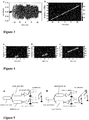
- Figure 3 shows test results for the generated full-spectrum covering wideband chirp signal, wherein (a) being the time domain waveform, and (b) being the short time Fourier transformation analysis.
- the signal range is 5-60 GHz, time width is ⁇ 23ns, and time bandwidth product is as high as ⁇ 1265.
- Figure 4 shows test results for short time Fourier analysis of the chip signals with various wavebands, wherein (a) depicting X waveband (8-12GHz), (b) Ku waveband (12-18GHz), and (c) Ka waveband (26.5-40GHz).
- the signals generated by the signal transmitter testify to the capacity of the ultra wide band radar system with full-spectrum covering or with any arbitrary waveband.
- the signal transmitter generates an X waveband radar signal to detect a target, while the signal receiver receives the echo signal for preliminary experiment verification.
- Figure 5 shows a schematic diagram of a single target detection and a double target detection for the embodiment employing X waveband signal generated by the present invention.
- signal transmission and signal reception adopt two independent X waveband horn antennas parallel to one another, with the detected target perpendicular to a metal surface along signal transmission direction.
- T/R components the same effect is achieved.
- bandwidth compression and down conversion for the echo signal from the transceiver module is realized by the transceiving system based on time stretching.
- the electrical signal is loaded via the electro-optical modulator onto the previously dispersion-chirped optical pulse carrier wave, forming a modulation optical signal corresponding to the electrical signal.
- the prerequisite of the filtering bandwidth of the third optical filter 3-4 being greater than that of the first optical filter 1-5 and that of the second optical filter 1-7, and by means of properly tuning the second tunable time delay module 3-2, echo signals from multiple targets are all capable of being loaded onto the optical carrier wave.
- Target detection employing chirp signals attains good target property, owing to dependency of ranging resolution on the bandwidth of the transmitted signal.
- Useful target information is then extracted from the analog-digitally converted signal by means of digital processing.
- Target ranging resolution remains in the accuracy prior to time stretching.
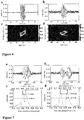
- Figure 7 shows time and distance test results between the targets in the double target detection.
- Figure 7(a) shows time the domain waveform subsequent to time stretching at a distance of ⁇ 6.3cm
- Figure 7(b) shows the time domain waveform subsequent to time stretching at a distance of ⁇ 15.0cm
- Figure 7(c) shows inter-positions of the both targets subsequent to matched filtering at a distance of ⁇ 6.3cm
- Figure 7(d) shows inter-positions of the both targets subsequent to matched filtering at a distance of ⁇ 15.0cm.
- the X waveband signal albeit undergoing time stretching and frequency compression in the signal receiver, retains the original ultra wideband detection accuracy.
Landscapes
- Engineering & Computer Science (AREA)
- Radar, Positioning & Navigation (AREA)
- Remote Sensing (AREA)
- Physics & Mathematics (AREA)
- Computer Networks & Wireless Communication (AREA)
- General Physics & Mathematics (AREA)
- Electromagnetism (AREA)
- Radar Systems Or Details Thereof (AREA)
- Optical Radar Systems And Details Thereof (AREA)
- Optical Communication System (AREA)
Abstract
Description
- The present invention relates to microwave optics and radar, and relates in particular to a full-spectrum covering ultra wideband full photonics-based radar system.
- Development of photonics since the eighties of the 20th century has initiated the proposal of the concept of full photonics-based radar, which has received wide attention from relevant researches at home and abroad. Photonics possesses the advantages of large bandwidth, low loss, and low jitter, with application thereof being capable of breaking the 'electronic bottleneck' existing in traditional microwave/millimeter-wave radar systems, thus furnishing a new technical channel for generation, reception, and processing of a higher frequency and larger bandwidth wideband signal. Directed at requirement for carrier frequency and agility by a radar system, the Italian P. Ghelfi et al realizes a full photonics-based coherent radar system (please refer to "A full photonics-based coherent radar system", P. Ghelfi, F. Laghezza, and F. Scotti, Nature, vol.507, no.7492, pp.341-345, 2014). Radar signal generation and reception in the system both comes from a same mode-locked laser, thus insuring high coherence of the system, effectively inhibiting jitter of phase noise, and increasing radar detection accuracy. The system proves to have a higher quantitative fidelity and detection accuracy in a validating demonstration with a 40GHZ narrow band radar. Due to the excellent property of the system, the research by P. Ghelfi et al has the potential to become a norm for designing the next generation radar system (please refer to "Technology: Photonics illuminates the future of radar", J. McKinney, Nature, 2014, vol.507, no. 7492, pp.310-312, Mar. 2014).
- A radar system, like those in other wireless techniques, may only properly works under pre-designed bandwidths. A multiband radar may simultaneously or in a cross gating manner works in multiple bands, and thus has a higher probability over a common radar to detect a target. Due to the multiple frequency components contained in a signal transmitted by a multiband wideband radar, it is capable of breaking the wave-absorbing effect of narrowband frequency absorption materials, thus effectively increasing the anti stealth detection capability thereof. A multiband radar is further advantageous in inhibiting and dodging enemy ejected interference, which is crucial in increasing detection capability, in decreasing multipath loss and in strengthening self survival rate. (Please refer to "Multiband Radar [C], Proceedings of The Fifteenth Annual Meeting of the Professional Radar Information Network of the Ministry of Industry and Information Technology, Su Bingrong, He Bingfa")
- In actual applications, a microwave/millimeter-wave radar generally employs the following signal waveforms: short pulse signal, phase-coded signal, or chirp signal. Transmission and receiving techniques are very hard to implement for a short pulse signal, due to the extremely stringent requirement for the pulses thereof in high precision ranging, i.e., the requirement for an extremely narrow pulse width. A phase-coded signal is realized by loading phase information onto a continuous carrier wave according to defined time intervals, albeit has a comparatively high precision and sidelobe suppression ratio, is not suitable for a wideband system, due to the difficult implementation and its susceptibility to Doppler effect and limitation by its own dynamic range. In contrast, a chirp signal is widely employed in high precision ranging and radar detection, with ranging accuracy dependent on its modulated bandwidth, and is an ideal choice for a microwave/millimeter-wave radar.
- The object of the present invention is to provide a full-spectrum covering ultra wideband full-photonics based radar system by overcoming the defects of the prior art. A same mode-locked laser with low jitter and wide spectrum is adopted for respectively generating and receiving an ultra wideband chirp signal to guarantee high coherence and high detection precision for the transceiver system. A signal transmitter realizes continuous tunability for center frequency, bandwidth and time width of an ultra wideband signal by making use of the wide spectrum of the mode-locked laser and an unbalanced dispersion chirp on both arms thereof, thus realizing full-spectrum coverage and generation of the ultra wideband signal with any arbitrary operating waveband. A signal receiver greatly mitigates back-end analog-digital converting and processing pressure by making use of time stretching in compressing the center frequency and bandwidth of the wideband signal, with target range resolution still remaining in the accuracy prior to time stretching.
- The technical solution for realizing the afore-mentioned object is as follows:
A full-spectrum covering ultra wideband full-photonics based radar system is provided, which comprises a signal transmitter, a transceiver module, and a signal receiver; the signal transmitter comprises a mode-locked laser, a first dispersion module, a first optical coupler, a second optical coupler, a first optical filter, a second dispersion module, a second optical filter, a first tunable time delay module, a third optical coupler, an optical amplifier, and a first photodetector; the transceiver module comprises a band selector, a first electrical amplifier array, a T/R component array, an antenna array, and a second electrical amplifier array; the signal receiver comprises a third optical filter, a second tunable time delay module, an electro-optical modulator, a third dispersion module, a second photodetector, an analog-digital conversion module, and a signal processing module; the inter relations of the above components are as follows:
An output end of the mode-locked laser is connected via the first dispersion module with an input end of the first optical coupler having a first output end and a second output end: the first output end of the first optical coupler is connected with an input end of the second optical coupler, the second optical coupler splits an optical path into a first optical path and a second optical path, with the first optical path traversing successively the first optical filter and the second dispersion module till an input end of the third optical coupler, the second optical path traversing successively the second optical filter and the first tunable time delay module till the input end of the third optical coupler; the third optical coupler couples a signal of the first optical path and of the second optical path respectively into one optical signal and outputs via the optical amplifier to enter the first photodetector, the first photodetector converts the optical signal into an electrical signal and inputs to an input end of the band selector of the transceiver module, the band selector having more than 2 output ends, with each said output end of the band selector connected successively with a respective electrical amplifier of the first electrical amplifier array, a respective T/R component of the T/R component array, and a respective antenna of the antenna array to form a channel for a respective waveband; an echo signal of an electrical signal transmitted from the antenna array is returned by a to be detected target and passes successively via the respective antenna of the antenna array, the respective T/R component of the T/R array and the second electrical amplifier array to form a target echo electrical signal to be inputted to an rf input end of the electro-optical modulator. - An optical signal of the second output end of the first optical coupler successively passes via the third optical filter and the second tunable time delay module to be inputted into an optical input end of the electro-optical modulator to form an optical pulse carrier wave.
- The electro-optical modulator loads the target echo electrical signal onto the optical pulse carrier wave to form an echo modulation optical signal corresponding to the target echo electrical signal, with the echo modulation optical signal of the electro-optical modulator successively passing via the third dispersion module, the second photodetector, and the analog-digital conversion module to enter the signal processing module.
- The mode-locked laser is a mode-locked laser with low jitter and wide spectrum.
- A filtering bandwidth of the third optical filter is greater than a filtering bandwidth of the first optical filter and that of the second optical filter.
- The principle for generation of the wideband chirp signal in the signal transmitter is based on spectral filtering and unbalanced dispersive chirping (please refer to H. Zhang, W. Zou, and J. Chen, "Generation of widely tunable linearly-chirped microwave waveform based on spectral filtering and unbalanced dispersion", Optics Letters, vol. 40, no. 6, pp. 1085-1088, 2015). By means of tuning the center wavelength and filtering bandwidth of the first tunable optical filter and those of the second optical filter, the center frequency and the sweep bandwidth of the wideband chirp signal is changed.
- While in the signal receiver, bandwidth compression and down conversion for the outputted signal from the transceiver module subsequent to electro-optical conversion is realized by means of borrowing from the principle of time stretching (please refer to Y. Han and B. Jalali, Photonic time-stretched analog-to-digital converter: Fundamental concepts and practical considerations, Journal of Lightwave Technology, vol. 21, no. 12, pp. 3085-3103, 2003). The radar echo signal is loaded via the electro-optical modulator onto the previously dispersion-chirped optical pulse carrier wave, forming the modulation optical signal corresponding to the radar echo signal. With the prerequisite of the filtering bandwidth of the third optical filter being greater than that of the first optical filter and that of the second optical filter, and by means of properly tuning the second tunable time delay module, echo signals from multiple targets are loaded onto the optical carrier wave. Subsequent to passing via the third dispersion module having much more dispersion, an electrical signal time-stretched multiple times of factor is obtained from the second photodetector. If the dispersion coefficients of the first dispersion module and the third dispersion module are respectively D1 and D3, then the stretch factor M is dependent thereon:

- Time stretching of the to be sampled rf signal is equivalent to compression in frequency domain, and thus pressure on bandwidth and sampling ratio for the back-end analog-digital converter is greatly mitigated. Useful target information is then extracted from the analog-digitally converted signal by means of digital processing, with target ranging resolution remaining in the accuracy prior to time stretching.
- The present invention is advantageous in the following aspects:
- 1. The signal transmitter and the signal receiver of the present invention are both based on the same mode-locked laser, thus insuring high coherence in signal generation and processing, and drastically increasing ranging detection accuracy for the present invention.
- 2. By means of tuning the first optical filter and the second optical filter, the present invention is capable of generating wideband chirp signal covering the full spectrum or with any specific waveband.
- 3. The present invention makes use of time stretching to time stretch the to be sampled signal and compress it in frequency domain, thus drastically mitigating pressure on bandwidth and sampling ratio for the back end analog-digital conversion module.
- 4. A switchable transceiving channel for the radar signals with full-spectrum covering or of multiple wavebands of the present invention is adopted, thus realizing uniform transceiving for the full spectrum of wavebands.
- 5. The target ranging resolution of the present invention is dependent on the bandwidth of the radar signal generated by the transmitter, and is not related to the time stretching factor.
-
-
Figure 1 is a schematic diagram for a structure of the full-spectrum covering ultra wideband full photonics-based radar system of the present invention. -
Figure 2 is a schematic diagram for a structure of the transceiver module. -
Figure 3 shows test results for characteristics of the full-spectrum covering wideband chirp signal, (a) time domain waveform, (b) short time Fourier transformation analysis. -
Figure 4 shows test results for short time Fourier analysis of the chip signals with various wavebands, (a) X waveband, (b) Ku waveband, and (c) Ka waveband. -
Figure 5 is a schematic diagram of an experiment of a single target detection and a double target detection for an embodiment employing the generated X waveband signal. -
Figure 6 shows test results for the time domain waveform and the short time Fourier analysis of the X waveband chirp signals prior to and subsequent to time stretching in the single target detection, (a) time domain prior to time stretching, (b) time domain subsequent to time stretching, (c) short time Fourier analysis prior to time stretching, (d) short time Fourier analysis subsequent to time stretching. -
Figure 7 shows time and distance test results between the targets in the double target detection, (a) time domain subsequent to time stretching at a distance of ~6.3cm, (b) time domain subsequent to time stretching at a distance of ~ 15.0cm, (c) inter-positions of the both targets subsequent to matched filtering at a distance of ~6.3cm, (d) inter-positions of the both targets subsequent to matched filtering at a distance of ∼15.0cm. - The present invention will be expounded in more details with the figures and an embodiment hereunder provided. The embodiment is implemented based on the technical solution of the present invention and provided with detailed implementing modes and specific operation procedures, but is not meant to limit the scope of protection of the present invention.
-
Figure 1 is a schematic diagram for a structure of the full-spectrum covering ultra wideband full photonics-based radar system of the present invention. As is shown therein, the full-spectrum covering ultra wideband full-photonics based radar system comprises asignal transmitter 1, atransceiver module 2, and asignal receiver 3. The signal transmitter comprises a mode-locked laser 1-1, a first dispersion module 1-2, a first optical coupler 1-3, a second optical coupler 1-4, a first optical filter 1-5, a second dispersion module 1-6, a second optical filter 1-7, a first tunable time delay module 1-8, a third optical coupler 1-9, an optical amplifier 1-10, and a first photodetector 1-11. - The signal receiver comprises 3 a third optical filter 3-1, a second tunable time delay module 3-2, an electro-optical modulator 3-3, a third dispersion module 3-4, a second photodetector 3-5, an analog-digital conversion module 3-6, and a signal processing module 3-7.
-
Figure 2 is a schematic diagram for a structure of thetransceiver module 2. As is shown therein, thetransceiver module 3 comprises a band selector 2-1, a first electrical amplifier array 2-2, a T/R component array 2-3, an antenna array 2-4, and a second electrical amplifier array 2-5. - The inter relations of the above components are as follows:
A pulse signal outputted by the mode-locked laser 1-1 firstly passes via the first dispersion module 1-2, and is subsequently split into two parts the first optical coupler 1-3, with the first part entering the second optical coupler 1-4, and the remaining part entering the third optical filter 3-1. The second optical coupler 1-4 splits the optical path into a first optical path and a second optical path, with the first optical path traversing successively the first optical filter 1-5 and the second dispersion module 1-6 till the third optical coupler 1-9, the second optical path traversing successively the second optical filter 1-7 and the first tunable time delay module 1-8 till the third optical coupler 1-9. The third optical coupler couples a signal of the first optical path and of the second optical path respectively into one optical signal and enters successively the optical amplifier 1-10 and the first photodetector 1-11. The first photodetector 1-11 converts the optical signal into an electrical signal and is inputted to the transceiver module. The band selector 2-1 has multiple output ends, with each output end connected successively with the first electrical amplifier array 2-2, the T/R component array 2-3, and the antenna array 2-4 to form multiple channels. The band selector 2-1 switches the signal to a specific channel in accordance with the waveband of the signal. An echo signal of an electrical signal transmitted from the antenna array 2-4 is returned by a to be detected target and passes successively via the respective antenna of the antenna array, the respective T/R component of the T/R array and the second electrical amplifier array to enter an rf input end of the electro-optical modulator 3-3. The output signal of the electro-optical modulator 3-3 successively passes via the third dispersion module 3-4, the second photodetector 3-5, and the analog-digital conversion module 3-6 to enter the signal processing module 3-7. - The working principle of the present invention is as follows:
The wideband chirp signal generated by the signal transmitter as shown inFigure 1 is based on spectral filtering and unbalanced dispersive chirping on the first optical path and the second optical path. By means of tuning the center wavelength and filtering bandwidth of the first tunable optical filter 1-5 and those of the second optical filter 1-7, the center frequency and the sweep bandwidth of the wideband chirp signal is changed. -
Figure 2 shows the schematic diagram for the structure of the transceiver module. For a generated signal with a specific waveband, the band selector switches it to a corresponding channel. The transceiver module amplifies and then transmits via an antenna the signal generated by the signal transmitter, and subsequently receives and amplifies the echo signal. -
Figure 3 shows test results for the generated full-spectrum covering wideband chirp signal, wherein (a) being the time domain waveform, and (b) being the short time Fourier transformation analysis. The signal range is 5-60 GHz, time width is ∼23ns, and time bandwidth product is as high as ∼1265. -
Figure 4 shows test results for short time Fourier analysis of the chip signals with various wavebands, wherein (a) depicting X waveband (8-12GHz), (b) Ku waveband (12-18GHz), and (c) Ka waveband (26.5-40GHz). The signals generated by the signal transmitter testify to the capacity of the ultra wide band radar system with full-spectrum covering or with any arbitrary waveband. - In order to verify the feasibility of the present invention, the signal transmitter generates an X waveband radar signal to detect a target, while the signal receiver receives the echo signal for preliminary experiment verification.
Figure 5 shows a schematic diagram of a single target detection and a double target detection for the embodiment employing X waveband signal generated by the present invention. As is shown inFigures 5(a) and (b) , signal transmission and signal reception adopt two independent X waveband horn antennas parallel to one another, with the detected target perpendicular to a metal surface along signal transmission direction. For a transmitting and receiving antenna comprising T/R components, the same effect is achieved. - In the signal receiver, bandwidth compression and down conversion for the echo signal from the transceiver module is realized by the transceiving system based on time stretching. On the basis of the principle of time stretching, the electrical signal is loaded via the electro-optical modulator onto the previously dispersion-chirped optical pulse carrier wave, forming a modulation optical signal corresponding to the electrical signal. With the prerequisite of the filtering bandwidth of the third optical filter 3-4 being greater than that of the first optical filter 1-5 and that of the second optical filter 1-7, and by means of properly tuning the second tunable time delay module 3-2, echo signals from multiple targets are all capable of being loaded onto the optical carrier wave. Subsequent to passing via the third dispersion module 3-4 having much more dispersion, an electrical signal time-stretched multiple times of factor is obtained from the second photodetector 3-5. Time stretching of the to be sampled rf signal is equivalent to compression in frequency domain, and thus pressure on bandwidth and sampling ratio for the back-end analog-digital conversion module 3-6 is greatly mitigated.
Figures 6(a) and (c) respectively show test results for the time domain waveform and the short time Fourier analysis of the X waveband signal, while Figures (c) and (d) respectively show test results for the time domain waveform and the short time Fourier analysis of the reflected X waveband echo signal subsequent to time stretching. Subsequent to time stretching, the X waveband signal is stretched intime domain 5 times over the original time, while frequency and bandwidth are compressed about 5 times. The compressed frequency and bandwidth subsequent to time stretching testifies to mitigation of pressure on back end signal quantization processing. - Target detection employing chirp signals attains good target property, owing to dependency of ranging resolution on the bandwidth of the transmitted signal. Useful target information is then extracted from the analog-digitally converted signal by means of digital processing. Target ranging resolution remains in the accuracy prior to time stretching.
Figure 7 shows time and distance test results between the targets in the double target detection.Figure 7(a) shows time the domain waveform subsequent to time stretching at a distance of ~6.3cm,Figure 7(b) shows the time domain waveform subsequent to time stretching at a distance of ∼15.0cm,Figure 7(c) shows inter-positions of the both targets subsequent to matched filtering at a distance of ~6.3cm, whileFigure 7(d) shows inter-positions of the both targets subsequent to matched filtering at a distance of ∼15.0cm. The X waveband signal, albeit undergoing time stretching and frequency compression in the signal receiver, retains the original ultra wideband detection accuracy.
Claims (3)
- A full-spectrum covering ultra wideband full-photonics based radar system, comprising a signal transmitter (1), a transceiver module (2), and a signal receiver (3); wherein the signal transmitter (1) comprises a mode-locked laser (1-1), a first dispersion module (1-2), a first optical coupler (1-3), a second optical coupler (1-4), a first optical filter (1-5), a second dispersion module (1-6), a second optical filter (1-7), a first tunable time delay module (1-8), a third optical coupler (1-9), an optical amplifier (1-10), and a first photodetector (1-11); the transceiver module (2) comprises a band selector (2-1), a first electrical amplifier array (2-2), a T/R component array (2-3), an antenna array (2-4), and a second electrical amplifier array (2-5); the signal receiver (3) comprises a third optical filter (3-1), a second tunable time delay module (3-2), an electro-optical modulator (3-3), a third dispersion module (3-4), a second photodetector (3-5), an analog-digital conversion module (3-6), and a signal processing module (3-7); an output end of the mode-locked laser (1-1) is connected via the first dispersion module (1-2) with an input end of the first optical coupler (1-3) having a first output end and a second output end: the first output end of the first optical coupler (1-3) is connected with an input end of the second optical coupler (1-4), the second optical coupler (1-4) splits an optical path into a first optical path and a second optical path, with the first optical path traversing successively the first optical filter (1-5) and the second dispersion module (1-6) till an input end of the third optical coupler (1-9), the second optical path traversing successively the second optical filter (1-7) and the first tunable time delay module (1-8) till the input end of the third optical coupler (1-9); the third optical coupler (1-9) couples a signal of the first optical path and of the second optical path respectively into one optical signal and outputs via the optical amplifier (1-10) to enter the first photodetector (1-11), the first photodetector (1-11) converts the optical signal into an electrical signal and inputs to an input end of the band selector (2-1) of the transceiver module (2), the band selector (2-1) having more than 2 output ends, with each said output end of the band selector (2-1) connected successively with a respective electrical amplifier of the first electrical amplifier array (2-2), a respective T/R component of the T/R component array (2-3), and a respective antenna of the antenna array (2-4) to form a channel for a respective waveband; an echo signal of an electrical signal transmitted from the antenna array (2-4) is returned by a to be detected target and passes successively via the respective antenna of the antenna array (2-4), the respective T/R component of the T/R array (2-3) and the second electrical amplifier array (2-5) to form a target echo electrical signal to be inputted to an rf input end of the electro-optical modulator (3-3); an optical signal of the second output end of the first optical coupler (1-3) successively passes via the third optical filter (3-1) and the second tunable time delay module (3-2) to be inputted into an optical input end of the electro-optical modulator (3-3) to form an optical pulse carrier wave; the electro-optical modulator (3-3) loads the target echo electrical signal onto the optical pulse carrier wave to form an echo modulation optical signal corresponding to the target echo electrical signal, with the echo modulation optical signal of the electro-optical modulator (3-3) successively passing via the third dispersion module (3-4), the second photodetector (3-5), and the analog-digital conversion module (3-6) to enter the signal processing module (3-7).
- The full-spectrum covering ultra wideband full-photonics based radar system of claim 1, wherein the mode-locked laser is a mode-locked laser with low jitter and wide spectrum.
- The full-spectrum covering ultra wideband full-photonics based radar system of claim 1 or 2, wherein a filtering bandwidth of the third optical filter is greater than a filtering bandwidth of the first optical filter and of the second optical filter.
Applications Claiming Priority (2)
| Application Number | Priority Date | Filing Date | Title |
|---|---|---|---|
| CN201510501404.3A CN105137448B (en) | 2015-08-17 | 2015-08-17 | The full optical detection and ranging system of ultra wide band of all band covering |
| PCT/CN2015/088463 WO2017028335A1 (en) | 2015-08-17 | 2015-08-29 | Ultra-wide-band all-optical radar system covering all wavebands |
Publications (3)
| Publication Number | Publication Date |
|---|---|
| EP3324211A1 true EP3324211A1 (en) | 2018-05-23 |
| EP3324211A4 EP3324211A4 (en) | 2018-12-12 |
| EP3324211B1 EP3324211B1 (en) | 2019-10-23 |
Family
ID=54722854
Family Applications (1)
| Application Number | Title | Priority Date | Filing Date |
|---|---|---|---|
| EP15901539.5A Active EP3324211B1 (en) | 2015-08-17 | 2015-08-29 | Ultra-wide-band all-optical radar system covering all wavebands |
Country Status (4)
| Country | Link |
|---|---|
| US (1) | US10605921B2 (en) |
| EP (1) | EP3324211B1 (en) |
| CN (1) | CN105137448B (en) |
| WO (1) | WO2017028335A1 (en) |
Families Citing this family (22)
| Publication number | Priority date | Publication date | Assignee | Title |
|---|---|---|---|---|
| CN106230516B (en) * | 2016-08-31 | 2018-09-14 | 上海交通大学 | Radar communication based on microwave photon fights integral system |
| CN106940440B (en) * | 2017-03-22 | 2019-09-24 | 中国电子科技集团公司第三十八研究所 | A kind of transceiving integrated radar system of full optical link gain and application method |
| CN107102322A (en) * | 2017-05-02 | 2017-08-29 | 哈尔滨工业大学 | Microwave laser radar integral system |
| US11310869B2 (en) * | 2017-09-27 | 2022-04-19 | Apple Inc. | RF radiohead with optical interconnection to baseband processor |
| WO2020019153A1 (en) * | 2018-07-24 | 2020-01-30 | 中国科学技术大学 | Femtosecond laser radar and gas composition detection method |
| CN109613510B (en) * | 2019-01-21 | 2020-09-04 | 杭州光预科技有限公司 | Microwave photon radar implementation method and system for small target detection or real-time tracking imaging |
| CN109884655B (en) * | 2019-03-21 | 2023-04-07 | 西南大学 | Light-carrying frequency modulation continuous wave laser ranging system based on light injection semiconductor laser |
| CN109975768B (en) * | 2019-05-15 | 2024-04-09 | 成都锦江电子系统工程有限公司 | Ka wave band frequency synthesizer based on radar |
| CN111142089B (en) * | 2020-01-10 | 2021-09-21 | 清华大学 | OBFN and PADC function integrated broadband radar signal receiving device and method |
| CN111277340B (en) * | 2020-01-20 | 2021-12-03 | 杭州仁牧科技有限公司 | High-power broadband emission array actual measurement system and test method thereof |
| CN111404547B (en) * | 2020-03-25 | 2022-06-28 | 北京大学 | A kind of broadband millimeter wave signal analog-to-digital conversion method and system |
| CN111565075A (en) * | 2020-04-15 | 2020-08-21 | 西北工业大学 | A broadband microwave photonic phase encoding signal generating device and method |
| CN111948633B (en) * | 2020-06-29 | 2022-11-29 | 北京理工大学 | Flexible ultra-wideband digital microwave photon phased array radar |
| CN113093153B (en) * | 2021-04-12 | 2022-12-30 | 中国科学院半导体研究所 | Receiving and transmitting integrated beam forming network system based on dispersion delay |
| CN113985388B (en) * | 2021-10-22 | 2026-03-10 | 上海交通大学 | Broadband radar receiver based on photon time stretching |
| CN114244448B (en) * | 2022-01-27 | 2023-03-14 | 上海交通大学 | Optical millimeter wave/terahertz transmission system and transmission method based on passive phase compensation |
| CN115079139B (en) * | 2022-06-29 | 2025-05-06 | 上海交通大学 | Photon time-stretching coherent radar chip |
| US12566240B2 (en) * | 2023-10-25 | 2026-03-03 | City University Of Hong Kong | Integrated lithium niobate photonic millimeter-wave radar |
| CN118859132B (en) * | 2024-08-22 | 2025-08-29 | 南昌华梦达航空科技发展有限公司 | An ultra-wide spectrum radar system |
| CN119210601B (en) * | 2024-09-02 | 2025-10-24 | 上海交通大学 | Multi-band shared phased array transceiver system based on optical pulse and its implementation method |
| CN119363242B (en) * | 2024-10-23 | 2026-04-07 | 中国人民解放军空军预警学院 | Signal processing method and system based on microwave photon technology and electronic equipment |
| CN119544085B (en) * | 2024-11-29 | 2025-09-26 | 西安电子工程研究所 | Ultra-wideband light electromagnetic reconnaissance receiver based on electro-optic sensing |
Family Cites Families (12)
| Publication number | Priority date | Publication date | Assignee | Title |
|---|---|---|---|---|
| US6731829B2 (en) * | 2000-12-16 | 2004-05-04 | Hrl Laboratories, Llc. | True-time all-optical delay generator for array beam steerers |
| GB2421336A (en) * | 2004-11-19 | 2006-06-21 | Filtronic Plc | Generating an arbitrary waveform wide band electrical signal |
| CN102937586B (en) * | 2012-11-01 | 2015-01-14 | 南京信息工程大学 | Laser radar based water-in-cloud raman scattering full-spectrum measurement system and method thereof |
| CN103064199A (en) * | 2012-12-10 | 2013-04-24 | 上海交通大学 | Reflection-type adjustable light delay line |
| CN103166706B (en) * | 2013-02-05 | 2016-03-30 | 上海交通大学 | Based on the photoelectric oscillation device of the frequency-tunable of wide spectrum light source |
| US9683928B2 (en) * | 2013-06-23 | 2017-06-20 | Eric Swanson | Integrated optical system and components utilizing tunable optical sources and coherent detection and phased array for imaging, ranging, sensing, communications and other applications |
| CN103941235B (en) * | 2014-02-26 | 2016-07-06 | 上海交通大学 | Full Optical Controlled Phased Array Antenna transmitter |
| CN103913645B (en) * | 2014-03-31 | 2016-08-17 | 南京航空航天大学 | Fibre optic sensor arra and antenna pattern measurement device, measuring method |
| EP3164953B1 (en) * | 2014-07-01 | 2018-12-05 | Telefonaktiebolaget LM Ericsson (publ) | Feed signal generation for a phased array antenna |
| CN104333421B (en) * | 2014-08-28 | 2016-09-14 | 中国科学院半导体研究所 | Triangular pulse signal generation device based on all-optical integrator |
| CN104570545B (en) * | 2015-01-22 | 2017-07-14 | 上海交通大学 | The generation device of all-optical, tunable wideband correlation |
| CN104733985A (en) * | 2015-04-09 | 2015-06-24 | 中国科学院半导体研究所 | Microwave pulse generation device based on Leo optical filter |
-
2015
- 2015-08-17 CN CN201510501404.3A patent/CN105137448B/en active Active
- 2015-08-29 WO PCT/CN2015/088463 patent/WO2017028335A1/en not_active Ceased
- 2015-08-29 EP EP15901539.5A patent/EP3324211B1/en active Active
-
2017
- 2017-12-06 US US15/833,992 patent/US10605921B2/en active Active
Also Published As
| Publication number | Publication date |
|---|---|
| WO2017028335A1 (en) | 2017-02-23 |
| US10605921B2 (en) | 2020-03-31 |
| EP3324211B1 (en) | 2019-10-23 |
| US20180106904A1 (en) | 2018-04-19 |
| EP3324211A4 (en) | 2018-12-12 |
| CN105137448B (en) | 2017-07-28 |
| CN105137448A (en) | 2015-12-09 |
Similar Documents
| Publication | Publication Date | Title |
|---|---|---|
| EP3324211B1 (en) | Ultra-wide-band all-optical radar system covering all wavebands | |
| CN108845296B (en) | A broadband radar radio frequency digital receiver and signal acquisition and processing method based on microwave photons | |
| Ma et al. | Microwave photonic imaging radar with a sub-centimeter-level resolution | |
| Ghelfi et al. | Photonics for radars operating on multiple coherent bands | |
| Zou et al. | All-optical central-frequency-programmable and bandwidth-tailorable radar | |
| Peng et al. | A photonics-based coherent dual-band radar for super-resolution range profile | |
| CN115184943B (en) | A terahertz radar detection method and system based on photon technology | |
| Ma et al. | High-resolution microwave photonic radar with sparse stepped frequency chirp signals | |
| Scotti et al. | In-field experiments of the first photonics-based software-defined coherent radar | |
| CN110221292B (en) | A microwave photonic multi-band radar imaging system and method | |
| Melo et al. | Dual-use system combining simultaneous active radar & communication, based on a single photonics-assisted transceiver | |
| Laghezza et al. | Field evaluation of a photonics‐based radar system in a maritime environment compared to a reference commercial sensor | |
| Cheng et al. | Photonic generation of programmable coherent linear frequency modulated signal and its application in X-band radar system | |
| US20230236285A1 (en) | A radar system having a photonics-based signal generator | |
| US10698095B1 (en) | Systems and methods and performing offset IQ modulation | |
| CN114614841B (en) | Photonic millimeter wave radar communication integrated system based on analog phase modulation | |
| Wang et al. | Dual-band THz photonic pulses enabling synthetic mm-scale range resolution | |
| Zhu et al. | High-resolution detection by multiband fusion of photonics-based radars | |
| Gao et al. | Photonics-based multiband radar applying an optical frequency sweeping comb and photonic dechirp receiving | |
| CN112782671B (en) | Broadband microwave photon radar real-time receiving device based on cross correlation | |
| CN113985388B (en) | Broadband radar receiver based on photon time stretching | |
| CN210775831U (en) | Radar apparatus | |
| Laghezza et al. | Photonic based marine radar demonstrator | |
| Chen et al. | Reconfigurable microwave photonics radars | |
| Zhang et al. | RF channelization technology |
Legal Events
| Date | Code | Title | Description |
|---|---|---|---|
| STAA | Information on the status of an ep patent application or granted ep patent |
Free format text: STATUS: THE INTERNATIONAL PUBLICATION HAS BEEN MADE |
|
| PUAI | Public reference made under article 153(3) epc to a published international application that has entered the european phase |
Free format text: ORIGINAL CODE: 0009012 |
|
| STAA | Information on the status of an ep patent application or granted ep patent |
Free format text: STATUS: REQUEST FOR EXAMINATION WAS MADE |
|
| 17P | Request for examination filed |
Effective date: 20180105 |
|
| AK | Designated contracting states |
Kind code of ref document: A1 Designated state(s): AL AT BE BG CH CY CZ DE DK EE ES FI FR GB GR HR HU IE IS IT LI LT LU LV MC MK MT NL NO PL PT RO RS SE SI SK SM TR |
|
| AX | Request for extension of the european patent |
Extension state: BA ME |
|
| RIN1 | Information on inventor provided before grant (corrected) |
Inventor name: ZHANG, HAO Inventor name: ZOU, WEIWEN Inventor name: CHEN, JIANPING Inventor name: ZHANG, SITENG |
|
| REG | Reference to a national code |
Ref country code: DE Ref legal event code: R079 Ref document number: 602015040546 Country of ref document: DE Free format text: PREVIOUS MAIN CLASS: G01S0017880000 Ipc: G01S0013260000 |
|
| DAV | Request for validation of the european patent (deleted) | ||
| DAX | Request for extension of the european patent (deleted) | ||
| A4 | Supplementary search report drawn up and despatched |
Effective date: 20181108 |
|
| RIC1 | Information provided on ipc code assigned before grant |
Ipc: G01S 13/26 20060101AFI20181102BHEP Ipc: G01S 7/28 20060101ALI20181102BHEP Ipc: G01S 7/03 20060101ALI20181102BHEP |
|
| GRAP | Despatch of communication of intention to grant a patent |
Free format text: ORIGINAL CODE: EPIDOSNIGR1 |
|
| STAA | Information on the status of an ep patent application or granted ep patent |
Free format text: STATUS: GRANT OF PATENT IS INTENDED |
|
| INTG | Intention to grant announced |
Effective date: 20190514 |
|
| GRAS | Grant fee paid |
Free format text: ORIGINAL CODE: EPIDOSNIGR3 |
|
| GRAA | (expected) grant |
Free format text: ORIGINAL CODE: 0009210 |
|
| STAA | Information on the status of an ep patent application or granted ep patent |
Free format text: STATUS: THE PATENT HAS BEEN GRANTED |
|
| AK | Designated contracting states |
Kind code of ref document: B1 Designated state(s): AL AT BE BG CH CY CZ DE DK EE ES FI FR GB GR HR HU IE IS IT LI LT LU LV MC MK MT NL NO PL PT RO RS SE SI SK SM TR |
|
| REG | Reference to a national code |
Ref country code: GB Ref legal event code: FG4D |
|
| REG | Reference to a national code |
Ref country code: CH Ref legal event code: EP |
|
| REG | Reference to a national code |
Ref country code: IE Ref legal event code: FG4D |
|
| REG | Reference to a national code |
Ref country code: DE Ref legal event code: R096 Ref document number: 602015040546 Country of ref document: DE |
|
| REG | Reference to a national code |
Ref country code: AT Ref legal event code: REF Ref document number: 1194275 Country of ref document: AT Kind code of ref document: T Effective date: 20191115 |
|
| REG | Reference to a national code |
Ref country code: NL Ref legal event code: MP Effective date: 20191023 |
|
| REG | Reference to a national code |
Ref country code: LT Ref legal event code: MG4D |
|
| PG25 | Lapsed in a contracting state [announced via postgrant information from national office to epo] |
Ref country code: PT Free format text: LAPSE BECAUSE OF FAILURE TO SUBMIT A TRANSLATION OF THE DESCRIPTION OR TO PAY THE FEE WITHIN THE PRESCRIBED TIME-LIMIT Effective date: 20200224 Ref country code: FI Free format text: LAPSE BECAUSE OF FAILURE TO SUBMIT A TRANSLATION OF THE DESCRIPTION OR TO PAY THE FEE WITHIN THE PRESCRIBED TIME-LIMIT Effective date: 20191023 Ref country code: LT Free format text: LAPSE BECAUSE OF FAILURE TO SUBMIT A TRANSLATION OF THE DESCRIPTION OR TO PAY THE FEE WITHIN THE PRESCRIBED TIME-LIMIT Effective date: 20191023 Ref country code: LV Free format text: LAPSE BECAUSE OF FAILURE TO SUBMIT A TRANSLATION OF THE DESCRIPTION OR TO PAY THE FEE WITHIN THE PRESCRIBED TIME-LIMIT Effective date: 20191023 Ref country code: SE Free format text: LAPSE BECAUSE OF FAILURE TO SUBMIT A TRANSLATION OF THE DESCRIPTION OR TO PAY THE FEE WITHIN THE PRESCRIBED TIME-LIMIT Effective date: 20191023 Ref country code: NL Free format text: LAPSE BECAUSE OF FAILURE TO SUBMIT A TRANSLATION OF THE DESCRIPTION OR TO PAY THE FEE WITHIN THE PRESCRIBED TIME-LIMIT Effective date: 20191023 Ref country code: GR Free format text: LAPSE BECAUSE OF FAILURE TO SUBMIT A TRANSLATION OF THE DESCRIPTION OR TO PAY THE FEE WITHIN THE PRESCRIBED TIME-LIMIT Effective date: 20200124 Ref country code: PL Free format text: LAPSE BECAUSE OF FAILURE TO SUBMIT A TRANSLATION OF THE DESCRIPTION OR TO PAY THE FEE WITHIN THE PRESCRIBED TIME-LIMIT Effective date: 20191023 Ref country code: NO Free format text: LAPSE BECAUSE OF FAILURE TO SUBMIT A TRANSLATION OF THE DESCRIPTION OR TO PAY THE FEE WITHIN THE PRESCRIBED TIME-LIMIT Effective date: 20200123 Ref country code: BG Free format text: LAPSE BECAUSE OF FAILURE TO SUBMIT A TRANSLATION OF THE DESCRIPTION OR TO PAY THE FEE WITHIN THE PRESCRIBED TIME-LIMIT Effective date: 20200123 |
|
| PG25 | Lapsed in a contracting state [announced via postgrant information from national office to epo] |
Ref country code: IS Free format text: LAPSE BECAUSE OF FAILURE TO SUBMIT A TRANSLATION OF THE DESCRIPTION OR TO PAY THE FEE WITHIN THE PRESCRIBED TIME-LIMIT Effective date: 20200224 Ref country code: HR Free format text: LAPSE BECAUSE OF FAILURE TO SUBMIT A TRANSLATION OF THE DESCRIPTION OR TO PAY THE FEE WITHIN THE PRESCRIBED TIME-LIMIT Effective date: 20191023 Ref country code: RS Free format text: LAPSE BECAUSE OF FAILURE TO SUBMIT A TRANSLATION OF THE DESCRIPTION OR TO PAY THE FEE WITHIN THE PRESCRIBED TIME-LIMIT Effective date: 20191023 |
|
| PG25 | Lapsed in a contracting state [announced via postgrant information from national office to epo] |
Ref country code: AL Free format text: LAPSE BECAUSE OF FAILURE TO SUBMIT A TRANSLATION OF THE DESCRIPTION OR TO PAY THE FEE WITHIN THE PRESCRIBED TIME-LIMIT Effective date: 20191023 |
|
| REG | Reference to a national code |
Ref country code: DE Ref legal event code: R097 Ref document number: 602015040546 Country of ref document: DE |
|
| PG2D | Information on lapse in contracting state deleted |
Ref country code: IS |
|
| PG25 | Lapsed in a contracting state [announced via postgrant information from national office to epo] |
Ref country code: DK Free format text: LAPSE BECAUSE OF FAILURE TO SUBMIT A TRANSLATION OF THE DESCRIPTION OR TO PAY THE FEE WITHIN THE PRESCRIBED TIME-LIMIT Effective date: 20191023 Ref country code: ES Free format text: LAPSE BECAUSE OF FAILURE TO SUBMIT A TRANSLATION OF THE DESCRIPTION OR TO PAY THE FEE WITHIN THE PRESCRIBED TIME-LIMIT Effective date: 20191023 Ref country code: RO Free format text: LAPSE BECAUSE OF FAILURE TO SUBMIT A TRANSLATION OF THE DESCRIPTION OR TO PAY THE FEE WITHIN THE PRESCRIBED TIME-LIMIT Effective date: 20191023 Ref country code: CZ Free format text: LAPSE BECAUSE OF FAILURE TO SUBMIT A TRANSLATION OF THE DESCRIPTION OR TO PAY THE FEE WITHIN THE PRESCRIBED TIME-LIMIT Effective date: 20191023 Ref country code: EE Free format text: LAPSE BECAUSE OF FAILURE TO SUBMIT A TRANSLATION OF THE DESCRIPTION OR TO PAY THE FEE WITHIN THE PRESCRIBED TIME-LIMIT Effective date: 20191023 Ref country code: IS Free format text: LAPSE BECAUSE OF FAILURE TO SUBMIT A TRANSLATION OF THE DESCRIPTION OR TO PAY THE FEE WITHIN THE PRESCRIBED TIME-LIMIT Effective date: 20200223 |
|
| REG | Reference to a national code |
Ref country code: AT Ref legal event code: MK05 Ref document number: 1194275 Country of ref document: AT Kind code of ref document: T Effective date: 20191023 |
|
| PLBE | No opposition filed within time limit |
Free format text: ORIGINAL CODE: 0009261 |
|
| STAA | Information on the status of an ep patent application or granted ep patent |
Free format text: STATUS: NO OPPOSITION FILED WITHIN TIME LIMIT |
|
| PG25 | Lapsed in a contracting state [announced via postgrant information from national office to epo] |
Ref country code: SK Free format text: LAPSE BECAUSE OF FAILURE TO SUBMIT A TRANSLATION OF THE DESCRIPTION OR TO PAY THE FEE WITHIN THE PRESCRIBED TIME-LIMIT Effective date: 20191023 Ref country code: SM Free format text: LAPSE BECAUSE OF FAILURE TO SUBMIT A TRANSLATION OF THE DESCRIPTION OR TO PAY THE FEE WITHIN THE PRESCRIBED TIME-LIMIT Effective date: 20191023 |
|
| 26N | No opposition filed |
Effective date: 20200724 |
|
| PG25 | Lapsed in a contracting state [announced via postgrant information from national office to epo] |
Ref country code: SI Free format text: LAPSE BECAUSE OF FAILURE TO SUBMIT A TRANSLATION OF THE DESCRIPTION OR TO PAY THE FEE WITHIN THE PRESCRIBED TIME-LIMIT Effective date: 20191023 Ref country code: AT Free format text: LAPSE BECAUSE OF FAILURE TO SUBMIT A TRANSLATION OF THE DESCRIPTION OR TO PAY THE FEE WITHIN THE PRESCRIBED TIME-LIMIT Effective date: 20191023 |
|
| PG25 | Lapsed in a contracting state [announced via postgrant information from national office to epo] |
Ref country code: MC Free format text: LAPSE BECAUSE OF FAILURE TO SUBMIT A TRANSLATION OF THE DESCRIPTION OR TO PAY THE FEE WITHIN THE PRESCRIBED TIME-LIMIT Effective date: 20191023 |
|
| REG | Reference to a national code |
Ref country code: CH Ref legal event code: PL |
|
| GBPC | Gb: european patent ceased through non-payment of renewal fee |
Effective date: 20200829 |
|
| PG25 | Lapsed in a contracting state [announced via postgrant information from national office to epo] |
Ref country code: CH Free format text: LAPSE BECAUSE OF NON-PAYMENT OF DUE FEES Effective date: 20200831 Ref country code: LI Free format text: LAPSE BECAUSE OF NON-PAYMENT OF DUE FEES Effective date: 20200831 Ref country code: LU Free format text: LAPSE BECAUSE OF NON-PAYMENT OF DUE FEES Effective date: 20200829 |
|
| PG25 | Lapsed in a contracting state [announced via postgrant information from national office to epo] |
Ref country code: GB Free format text: LAPSE BECAUSE OF NON-PAYMENT OF DUE FEES Effective date: 20200829 Ref country code: IE Free format text: LAPSE BECAUSE OF NON-PAYMENT OF DUE FEES Effective date: 20200829 |
|
| PG25 | Lapsed in a contracting state [announced via postgrant information from national office to epo] |
Ref country code: TR Free format text: LAPSE BECAUSE OF FAILURE TO SUBMIT A TRANSLATION OF THE DESCRIPTION OR TO PAY THE FEE WITHIN THE PRESCRIBED TIME-LIMIT Effective date: 20191023 Ref country code: MT Free format text: LAPSE BECAUSE OF FAILURE TO SUBMIT A TRANSLATION OF THE DESCRIPTION OR TO PAY THE FEE WITHIN THE PRESCRIBED TIME-LIMIT Effective date: 20191023 Ref country code: CY Free format text: LAPSE BECAUSE OF FAILURE TO SUBMIT A TRANSLATION OF THE DESCRIPTION OR TO PAY THE FEE WITHIN THE PRESCRIBED TIME-LIMIT Effective date: 20191023 |
|
| PG25 | Lapsed in a contracting state [announced via postgrant information from national office to epo] |
Ref country code: MK Free format text: LAPSE BECAUSE OF FAILURE TO SUBMIT A TRANSLATION OF THE DESCRIPTION OR TO PAY THE FEE WITHIN THE PRESCRIBED TIME-LIMIT Effective date: 20191023 |
|
| PGFP | Annual fee paid to national office [announced via postgrant information from national office to epo] |
Ref country code: DE Payment date: 20250812 Year of fee payment: 11 |
|
| PGFP | Annual fee paid to national office [announced via postgrant information from national office to epo] |
Ref country code: IT Payment date: 20250808 Year of fee payment: 11 |
|
| PGFP | Annual fee paid to national office [announced via postgrant information from national office to epo] |
Ref country code: BE Payment date: 20250826 Year of fee payment: 11 |
|
| PGFP | Annual fee paid to national office [announced via postgrant information from national office to epo] |
Ref country code: FR Payment date: 20250828 Year of fee payment: 11 |