EP3316448B1 - Wireless power reception apparatus - Google Patents
Wireless power reception apparatus Download PDFInfo
- Publication number
- EP3316448B1 EP3316448B1 EP16814764.3A EP16814764A EP3316448B1 EP 3316448 B1 EP3316448 B1 EP 3316448B1 EP 16814764 A EP16814764 A EP 16814764A EP 3316448 B1 EP3316448 B1 EP 3316448B1
- Authority
- EP
- European Patent Office
- Prior art keywords
- unit
- wireless power
- pattern
- soft magnetic
- transmission side
- Prior art date
- Legal status (The legal status is an assumption and is not a legal conclusion. Google has not performed a legal analysis and makes no representation as to the accuracy of the status listed.)
- Active
Links
- 239000002184 metal Substances 0.000 claims description 45
- 239000000758 substrate Substances 0.000 claims description 13
- 230000005540 biological transmission Effects 0.000 description 50
- 238000006243 chemical reaction Methods 0.000 description 35
- 238000004891 communication Methods 0.000 description 30
- 230000035699 permeability Effects 0.000 description 18
- 238000000034 method Methods 0.000 description 17
- 239000003990 capacitor Substances 0.000 description 14
- 230000006698 induction Effects 0.000 description 13
- 230000000694 effects Effects 0.000 description 11
- 239000002923 metal particle Substances 0.000 description 10
- 230000003252 repetitive effect Effects 0.000 description 10
- 230000015572 biosynthetic process Effects 0.000 description 6
- 238000010586 diagram Methods 0.000 description 6
- 238000005516 engineering process Methods 0.000 description 6
- 230000004907 flux Effects 0.000 description 6
- 230000003247 decreasing effect Effects 0.000 description 4
- 230000000052 comparative effect Effects 0.000 description 3
- 239000000463 material Substances 0.000 description 3
- 239000002952 polymeric resin Substances 0.000 description 3
- 229920003002 synthetic resin Polymers 0.000 description 3
- JOYRKODLDBILNP-UHFFFAOYSA-N Ethyl urethane Chemical compound CCOC(N)=O JOYRKODLDBILNP-UHFFFAOYSA-N 0.000 description 2
- 239000002131 composite material Substances 0.000 description 2
- 230000001276 controlling effect Effects 0.000 description 2
- 230000008878 coupling Effects 0.000 description 2
- 238000010168 coupling process Methods 0.000 description 2
- 238000005859 coupling reaction Methods 0.000 description 2
- 238000010304 firing Methods 0.000 description 2
- 239000000696 magnetic material Substances 0.000 description 2
- 238000012986 modification Methods 0.000 description 2
- 230000004048 modification Effects 0.000 description 2
- 239000000843 powder Substances 0.000 description 2
- 229910000859 α-Fe Inorganic materials 0.000 description 2
- 206010044334 Trance Diseases 0.000 description 1
- 229910045601 alloy Inorganic materials 0.000 description 1
- 239000000956 alloy Substances 0.000 description 1
- 230000001419 dependent effect Effects 0.000 description 1
- 238000009826 distribution Methods 0.000 description 1
- 239000011888 foil Substances 0.000 description 1
- 238000009499 grossing Methods 0.000 description 1
- 238000009413 insulation Methods 0.000 description 1
- 230000001788 irregular Effects 0.000 description 1
- 238000001646 magnetic resonance method Methods 0.000 description 1
- 230000005389 magnetism Effects 0.000 description 1
- 238000004519 manufacturing process Methods 0.000 description 1
- 239000007769 metal material Substances 0.000 description 1
- 238000003825 pressing Methods 0.000 description 1
- 230000008569 process Effects 0.000 description 1
- 230000005855 radiation Effects 0.000 description 1
- 230000001105 regulatory effect Effects 0.000 description 1
- 238000000926 separation method Methods 0.000 description 1
- 238000003860 storage Methods 0.000 description 1
- 230000001360 synchronised effect Effects 0.000 description 1
Images


Classifications
-
- H—ELECTRICITY
- H01—ELECTRIC ELEMENTS
- H01F—MAGNETS; INDUCTANCES; TRANSFORMERS; SELECTION OF MATERIALS FOR THEIR MAGNETIC PROPERTIES
- H01F27/00—Details of transformers or inductances, in general
- H01F27/24—Magnetic cores
- H01F27/25—Magnetic cores made from strips or ribbons
-
- H—ELECTRICITY
- H02—GENERATION; CONVERSION OR DISTRIBUTION OF ELECTRIC POWER
- H02J—CIRCUIT ARRANGEMENTS OR SYSTEMS FOR SUPPLYING OR DISTRIBUTING ELECTRIC POWER; SYSTEMS FOR STORING ELECTRIC ENERGY
- H02J50/00—Circuit arrangements or systems for wireless supply or distribution of electric power
- H02J50/10—Circuit arrangements or systems for wireless supply or distribution of electric power using inductive coupling
- H02J50/12—Circuit arrangements or systems for wireless supply or distribution of electric power using inductive coupling of the resonant type
-
- H—ELECTRICITY
- H01—ELECTRIC ELEMENTS
- H01F—MAGNETS; INDUCTANCES; TRANSFORMERS; SELECTION OF MATERIALS FOR THEIR MAGNETIC PROPERTIES
- H01F1/00—Magnets or magnetic bodies characterised by the magnetic materials therefor; Selection of materials for their magnetic properties
- H01F1/01—Magnets or magnetic bodies characterised by the magnetic materials therefor; Selection of materials for their magnetic properties of inorganic materials
- H01F1/03—Magnets or magnetic bodies characterised by the magnetic materials therefor; Selection of materials for their magnetic properties of inorganic materials characterised by their coercivity
- H01F1/12—Magnets or magnetic bodies characterised by the magnetic materials therefor; Selection of materials for their magnetic properties of inorganic materials characterised by their coercivity of soft-magnetic materials
- H01F1/14—Magnets or magnetic bodies characterised by the magnetic materials therefor; Selection of materials for their magnetic properties of inorganic materials characterised by their coercivity of soft-magnetic materials metals or alloys
- H01F1/16—Magnets or magnetic bodies characterised by the magnetic materials therefor; Selection of materials for their magnetic properties of inorganic materials characterised by their coercivity of soft-magnetic materials metals or alloys in the form of sheets
-
- H—ELECTRICITY
- H01—ELECTRIC ELEMENTS
- H01F—MAGNETS; INDUCTANCES; TRANSFORMERS; SELECTION OF MATERIALS FOR THEIR MAGNETIC PROPERTIES
- H01F27/00—Details of transformers or inductances, in general
- H01F27/34—Special means for preventing or reducing unwanted electric or magnetic effects, e.g. no-load losses, reactive currents, harmonics, oscillations, leakage fields
- H01F27/36—Electric or magnetic shields or screens
- H01F27/366—Electric or magnetic shields or screens made of ferromagnetic material
-
- H—ELECTRICITY
- H01—ELECTRIC ELEMENTS
- H01F—MAGNETS; INDUCTANCES; TRANSFORMERS; SELECTION OF MATERIALS FOR THEIR MAGNETIC PROPERTIES
- H01F38/00—Adaptations of transformers or inductances for specific applications or functions
- H01F38/14—Inductive couplings
-
- H—ELECTRICITY
- H02—GENERATION; CONVERSION OR DISTRIBUTION OF ELECTRIC POWER
- H02J—CIRCUIT ARRANGEMENTS OR SYSTEMS FOR SUPPLYING OR DISTRIBUTING ELECTRIC POWER; SYSTEMS FOR STORING ELECTRIC ENERGY
- H02J50/00—Circuit arrangements or systems for wireless supply or distribution of electric power
- H02J50/70—Circuit arrangements or systems for wireless supply or distribution of electric power involving the reduction of electric, magnetic or electromagnetic leakage fields
-
- H02J7/025—
-
- H04B5/79—
Definitions
- the present invention relates to a wireless power receiving apparatus
- Wireless power transmitting/receiving technology is a technology which wirelessly supplies power to electronic devices.
- a soft magnetic material may be disposed around a transmitting antenna and a receiving antenna so that electromagnetic energy radiated by the transmitting antenna can be focused in a direction of the receiving antenna.
- a soft magnetic layer is a sheet containing a ferrite material
- magnetic permeability is good, however, there is a limitation related to a thickness of the soft magnetic layer due to the limitation related to the high-temperature firing and magnetic flux density.
- a soft magnetic layer is a sheet which has a composite form containing a metal powder and a polymer resin, there is a problem in terms of lower magnetic permeability.
- a soft magnetic layer is a metal ribbon
- US 2014/239892 A1 discloses providing incisions in thin magnetic plates.
- Embodiments of the present invention provide a wireless power receiving apparatus and a wireless power transfer system including the wireless power receiving apparatus.
- the present invention relates to a wireless power receiving apparatus for charging power wirelessly as set out in claim 1.
- Embodiments of the invention are defined in dependent claims 2-6.
- a metal ribbon with high actual permeability within a frequency range which is used in wireless charging. Accordingly, it may be possible to obtain a wireless power transfer system not only having a slim shape but also having high efficiency in power transferring.
- Embodiments selectively use a variety type of frequency bands ranging from low frequency (50 kHz) to high frequency (15MHz) for wireless power transfer, and require support of a communication system capable of exchanging data and controlling signals for controlling system.
- Embodiments may be applied to various industrial fields such as a mobile terminal industry, a smart watch industry, a computer and laptop industry, a household appliances industry, an electric vehicle industry, a medical device industry and a robot industry, which use or require a battery.
- Embodiments may take into consideration a system capable of transferring power to at least one device using one or a plurality of transfer coils provided in the device.
- wireless power transfer technology is applied to household electrical appliances such as vacuum cleaners, fans, etc.
- household electrical appliances such as vacuum cleaners, fans, etc.
- complex wires can be eliminated in the home, which can reduce the amount of wiring in buildings and increase efficiency of the utility of space.
- it takes a lot of time to charge an electric car with a current household power source; however, when transferring high power through wireless power transfer technology, it is possible to reduce the charge time.
- a wireless charging facility on a floor of a parking lot, it is possible to eliminate inconvenience related to preparing a power cable near an electric car.
- one of the principles of wireless power transfer is related to a magnetic induction method.
- the magnetic induction method is a non-contact energy transfer technology in which an electromotive force is generated in a load inductor Ll via magnetic flux generated when a source inductor Ls and the load inductor Ll are brought to be close to each other and current is supplied to one of the source inductors Ls.
- Fig. 1 illustrates a diagram of a magnetic induction method equivalent circuit.
- the transmitting unit in a magnetic induction method equivalent circuit may be embodied by a source voltage Vs depending on an apparatus supplying power source, a source resistance Rs, a source capacitor Cs to match impedance and a source coil Ls to magnetically couple with a receiving unit, and the receiving unit may be shown by a load resistance R1 which is an equivalent resistance of the receiving unit, a load capacitor Cl to match impedance and a load coil Ll to magnetically couple with the transmitting unit, wherein a degree of magnetic coupling of the source coil Ls and the load coil Ll may be shown by mutual inductance Msl.
- equation 1 when a ratio of the inductance of the transmitting coil Ls to the source resistance Rs and a ratio of the load coil Ll to the load resistance Rl are the same, maximum power transfer becomes possible. Because there is no capacitors to compensate for reactance in a system in which only inductance is present, the self reflection value S11 of the input/output port at a point at which the maximum power delivery is created cannot be 0, and efficiency of power delivery may vary greatly based on the value of the mutual inductance Msl. Accordingly, the source capacitor Cs may be added to the transmitting unit as a compensation capacitor, and the load capacitor Cl may be added to the receiving unit.
- the compensation capacitors Cs and Cl may be connected in series or in parallel to, for example, the receiving coil Ls and the load coil Ll respectively.
- passive elements such as additional capacitors and inductors as well as the compensation capacitor may be added to each of the transmitting unit and the receiving unit.
- Fig. 2 is a block diagram showing a transmitting unit as one of the subsystems which constitute a wireless power transfer system.
- the wireless power transfer system may include a transmitting unit 1000 and a receiving unit 2000 to which power is wirelessly transferred from the transmitting unit 1000, wherein the transmitting unit 1000 may include an AC/DC conversion unit 1100 at the transmission side, a DC/AC conversion unit 1200 at the transmission side, an impedance matching unit 1300 at the transmission side, a transmitting coil unit 1400, and a communication and control unit 1500 at the transmission side.
- the transmitting unit 1000 may be alternatively used with a wireless power transmitting apparatus.
- the AC/DC conversion unit 1100 at the transmission side is a power conversion unit that converts an AC signal provided from the outside under the control of the communication and control unit 1500 at the transmission side into a DC signal
- the AC/DC conversion unit 1100 at the transmission side may include a rectifier 1110 and a DC/DC conversion unit 1120 at the transmission side as a subsystem.
- the rectifier 1110 is a system that converts an AC signal that has been provided into a DC signal and, as in the embodied examples, the rectifier 1110 may be a diode rectifier which has relatively high efficiency when operated at a high frequency, a synchronous rectifier which is capable of being a one-chip type or a hybrid rectifier which is able to save cost and space and have a high degree of freedom in Dead time.
- the AC/AC conversion unit 1120 at the transmission side regulates a level of an AC signal provided from the rectifier 1110 under the control of the communication and control unit 1500 at the transmission side, and as in the embodied examples, the AC/AC conversion unit 1120 may be a Buck converter which lowers a level of an input signal, a Boost converter which raises a level of an input signal, a Buck Boost converter which is able to lower or raise a level of an input signal, or a Cuk converter.
- the AC/AC conversion unit 1120 at the transmission side may include switch elements which serve as a power conversion control function, inductors and capacitors which serve a power conversion parameter role or serve as an output voltage smoothing function, trances which serve to regulate voltage gains or serve as an electrical separation function (an insulation function), etc., and the AC/AC conversion unit 1120 at the transmission side may serve to eliminate ripple components included in the input AC signal or to pulsate components (alternative components included in a AC signal). Furthermore, a difference between a command value of the output signal of the AC/AC conversion unit 1120 at the transmission side and an actual output value may be regulated via a feedback method, which can be performed through the communication and control unit 1500 at the transmission side.
- the DC/AC conversion unit 1200 at the transmission side is a system that converts an DC signal output from the AC/DC conversion unit 1100 at the transmission side under the control of the communication and control unit 1500 at the transmission side into a AC signal, and regulates a frequency of the converted AC signal, and as in the embodied examples, there is a Half bridge inverter or a Full bridge inverter.
- the DC/AC conversion unit 1200 at the transmission side may include oscillators which generate a frequency of the output signal and power amplifiers which amplify the output signal.
- the impedance matching unit 1300 at the transmission side improves a flow of a signal by minimizing a reflection wave at points having different impedance. Since the two coils of the transmitting unit 1000 and the receiving unit 2000 are spatially separated and thus leakage of the magnetic field is large, it is possible to improve the efficiency of the power delivery by correcting differences of the impedance between two connecting ends of the transmitting unit 1000 and the receiving unit 2000.
- the impedance matching unit 1300 at the transmission side may be composed of an inductor, a capacitor and a resistance element, and may regulate an impedance value to match the impedance by varying inductance of the inductor, capacitance of the capacitor and a value of resistance of the resistance element under the control of the communication and control unit 1500.
- the impedance matching unit 1300 at the transmission side may have a serial resonance structure or a parallel resonance structure, and it is possible to minimize energy loss by increasing an inductance coupling coefficient between the transmitting unit 1000 and the receiving unit 2000.
- the coil 1400 at the transmitting side may be embodied by a number of coils or a single coil.
- the coils may be arranged to be apart from each other, or arranged to be overlapped with each other.
- the overlapped area can be determined by taking into consideration of a deviation of a magnetic flux density.
- the coil 1400 may be manufactured by taking into consideration of internal resistance and radiation resistance. At that time, when the resistance component is small, the Quality factor can be increased and the transfer efficiency can be improved.
- the communication and control unit 1500 is a subsystem and may include a control unit 1510 at the transmission side and a communication unit 1520 at the transmission side.
- the control unit 1510 at the transmission side may serve to regulate the output voltage of the AC/DC conversion unit 1100 at the transmission side by taking into consideration of a required amount of power, a current amount of charge and the wireless power method of the receiving unit 2000.
- it is possible to control overall operation of the receiving unit 2000 by using an algorithm, a program, or an application required to control what is read from a storage unit (not shown) of the receiving unit 2000.
- control unit 1510 at the transmission side may be referred to as a microprocessor, a Micro Controller Unit or a Micom.
- the communication unit 1520 at the transmission side may communicate with a communication unit 2620 at a reception side, and a bluetooth method may be used as one example of a communication method.
- the communication unit 1520 at the transmission side and the communication unit 2620 at the reception side can transmit and receive charge status information and charge control commands and the like between each other.
- charge status information the number of the receiving units 2000, a remaining battery level, the number of charging, an amount of usage, a capacity of a battery, a ratio of a battery and a transfer amount of power of the transmitting unit 1000 may be included.
- the communication unit 1520 at the transmission side may transmit a charge function control signal which controls a charge function of the receiving unit 2000, and the charge function control signal may be a control signal that controls the receiving unit 2000 so as to enable or disable the charge function.
- the transmitting unit 1000 may composed of hardware which is different from that of the communication unit 1520 at the transmission side, therefore the transmitting unit 1000 may communicate with an out-band method.
- the transmitting unit 1000 and the communication unit 1520 at the transmission side may be embodied as one hardware unit, and therefore, the transmitting unit 1000 may communicate with an in-band method.
- the communication unit 1520 at the transmission side and the control unit 1510 at the transmitting side may be composed separately, and also in the receiving unit 2000, the communication unit 2620 at the reception side may be included in a control unit of the receiving apparatus or composed separately from the control unit thereof.
- Fig. 3 is a block diagram showing a receiving unit as one of the subsystems which constitutes a wireless power transfer system.
- the wireless power transfer system may include the transmitting unit 1000 and the receiving unit 2000 to which power is wirelessly transferred from the transmitting unit 1000, wherein the receiving unit 2000 may include a coil unit 2100 at the reception side, a matching unit 2200 at the reception side, an AC/DC conversion unit 2300 at the reception side, a DC/DC conversion unit 2400 at the reception unit, a load unit 2500 at the reception side and a communication and control unit 2600 at the reception side.
- the receiving unit 2000 may be alternatively used with a wireless power receiving apparatus.
- the coil unit 2100 at the reception side may receive power through a magnetic induction method, and a single induction coil or a plurality of induction coils may be provided.
- the coil unit 2100 at the reception side may be provided with an antenna for near field communication.
- the coil unit 2100 at the reception side may be the same as the coil unit 1400 at the transmission side.
- the size of the receiving antenna may depend on electrical characteristics of the receiving unit 2000.
- the matching unit 2200 at the reception side performs impedance matching between the transmitting unit 1000 and the receiving unit 2000.
- the AC/DC conversion unit 2300 at the reception side generates a DC signal by rectifying the AC signal, which is output from the coil unit 2100 at the reception side.
- the DC/DC conversion unit 2400 at the reception side can regulate a level of the DC signal, which is output from the AC/DC conversion unit 2300 at the reception unit, to be adapted to a capacity of the load unit 2500.
- the load unit 2500 may include a battery, a display, a sound output circuit, a main processor, and various sensors.
- the communication and control unit 2600 at the reception unit may be activated by wake-up power from the communication and control unit 1500 at the transmission side, perform communication with the communication and control unit 1500 at the transmission side, and control an operation of the subsystem of the receiving unit 2000.
- the receiving unit 2000 may be embodied in a single receiving unit or a plurality of receiving units, and energy can be wirelessly delivered from the transmitting unit 1000 simultaneously.
- a plurality of target receiving units 2000 may be supplied with power from one transmitting unit 1000 as a result of having a plurality of coil units at the reception side, which are independent of each other.
- the matching unit 1300 at the transmission side of the transmitting unit 1000 may adaptively perform impedance matching among the plurality of the receiving units 2000.
- the system of the receiving units 2000 may be of the same type or a different type.
- an AC signal of 60 Hz having 110V to 220V may be applied to the AC/DC conversion unit 1100 at the transmission side, and the AC/DC conversion unit 1100 may convert the AC signal into a DC signal having 10V to 20V and output the signal, and the DC signal may be applied to the DC/AC conversion unit 1200 at the transmission side, and the DC/AC conversion unit 1200 may output a AC signal of 125 KHZ.
- the AC signal of 125 KHz may be input to the AC/DC conversion unit 2300 at the reception side of the receiving unit 2000, and the AC/DC conversion unit 2300 may convert the AC signal into a DC signal having 10V to 20V, and the DC/DC conversion unit 2400 at the reception side may output a DC signal which is appropriate for the load unit 2500, for example, a DC signal having 5V, and deliver it to the load unit 2500.
- Fig. 4 is a drawing showing a part of a wireless power transmitting apparatus according to one embodiment of the present invention
- Fig. 5 is a drawing showing a part of a wireless power receiving apparatus according to one embodiment of the present invention.
- the wireless power transmitting apparatus may be a part of a component of the transmitting unit 1000
- the wireless power transmitting apparatus may be a part of a component of the receiving unit 2000.
- a wireless power transmitting apparatus 100 includes a transmitting circuit (not shown), a soft magnetic core 110, a transmitting coil 120 and a permanent magnet 130.
- the soft magnetic core 110 may be made of a soft magnetic material having a thickness of several mm.
- the permanent magnet 130 may be surrounded by the transmitting coil 120.
- the permanent magnet 130 is not an essential component, and may be omitted according to specifications.
- the wireless power receiving apparatus 200 includes a receiving circuit (not shown), a soft magnetic layer 210, and a receiving coil 220.
- the soft magnetic layer 210 may be laminated on a substrate (not shown).
- the substrate may be made of multiple layers of fixed sheets, may be bonded to the soft magnetic layer 210, and then make the soft magnetic layer 210 to be fixed.
- the soft magnetic layer 210 focuses electromagnetic energy which is radiated from the transmitting coil 120 of the wireless power transmitting apparatus 100.
- the receiving coil 220 is laminated on the soft magnetic layer 210.
- the receiving coil 220 may be wound in a parallel direction with the soft magnetic layer 210 on the soft magnetic layer 210.
- the receiving coil may be in a form of a spiral coil having an outer diameter of 50 mm or less and an inner diameter of 20 mm or more.
- the receiving circuit converts the received electromagnetic energy into electric energy via the receiving coil 220 and charges a battery (not shown) with the converted electric energy.
- a heat-radiating layer may be further included between the soft magnetic layer 210 and the receiving coil 220.
- a substrate, the soft magnetic layer 210 and the receiving coil 220 may be referred to as a receiving antenna.
- a NFC coil 230 may be further laminated on the soft magnetic layer 210.
- the NFC coil 230 may be configured to surround an outer circumference of the receiving coil 220.
- both of the receiving coil 220 and the NFC coil 230 may be electrically connected via terminals 240.
- the soft magnetic layer 210 is a sheet containing a ferrite, there is good magnetic permeability, however, there is a limitation related to a thickness of the soft magnetic layer due to the limitation with respect o high-temperature firing and magnetic flux density.
- the soft magnetic layer 210 is a sheet which has a composite form containing a metal powder and a polymer resin, there is a problem in terms of a lower magnetic permeability due to the polymer resin.
- the soft magnetic layer 210 is a metal ribbon, it is possible to attain high magnetic permeability and magnetic flux density with a thin thickness.
- the metal ribbon has a severe problem in terms of magnetic loss in a frequency area used for wireless charging.
- the soft magnetic layer 210 While a metal ribbon is used as the soft magnetic layer 210, it is intended to reduce eddy current loss caused by cracks being formed on the metal ribbon.
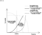
- Fig. 6 is a graph comparing actual permeability per frequency before and after a crack is formed on a metal ribbon.
- a difference between magnetic permeability and a loss of magnetic permeability may mean the actual permeability.
- the actual permeability after cracks are formed in the metal ribbon is significantly higher than the actual permeability before the cracks are formed.
- a metal ribbon means a noncrystalline or a nanocrystalline metal or an alloy made of very thin foil via techniques such as Atomizer.
- a thickness of the metal ribbon may be, for example, 0.01 mm to 0.04 mm.
- the metal ribbon may be a metal ribbon containing Fe.
- the metal ribbon As the soft magnetic layer 210 of the wireless power receiving apparatus 200, it is possible to reduce an eddy current loss and improve the efficiency of transfer by forming cracks on the metal ribbon.
- the effect of improving the transfer efficiency can be decreased, and the performance of the soft magnetic layer becomes ununiform so that a problem arises in that reliable results cannot be obtained.
- forming a uniform pattern of cracks on the metal ribbon is intended to improve the transfer efficiency of the soft magnetic layer, and to make the performance of the soft magnetic layer uniform.
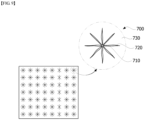
- Fig. 7 to Fig. 9 show top views of a soft magnetic substrate.
- a pattern including at least 3 lines 720 which are radiated from a predetermined point 710 is formed on the soft magnetic layer 210.
- the pattern may be formed as cracks.
- a plurality of patterns 700 may be formed repeatedly, and one pattern 700 may be arranged to be surrounded by a plurality of patterns, for example, by 3 to 8 patterns 700.
- a non-pattern area may be formed between the patterns.
- an average diameter of each pattern 700 may be 50 ⁇ m to 600 ⁇ m, preferably 75 ⁇ m to 500 ⁇ m, and more preferably 100 ⁇ m to 300 ⁇ m.
- the diameter of the pattern 700 is less than 50 ⁇ m, there may be a problem in terms of creating excess metal particles on a surface of the metal ribbon when forming cracks. In the case metal particles are present on the surface of the soft magnetic layer 210, there is a risk of circuit shorting because the metal particles may penetrate into the circuit.
- the diameter of the pattern 700 exceeds 600 ⁇ m, the effect of crack formation, that is, the effect of increasing the actual permeability may be decreased because the distance between the patterns 700 is great.
- Fig. 10 and Fig. 11 show top views of soft magnetic substrates.
- a pattern 700 including at least 3 lines 720 which are radiated from predetermined points 710, and an edge 730 which is surrounding the lines 720 is formed on the soft magnetic layer 210.
- the pattern may be formed as cracks.
- the edge 730 is not a crack which is completely cut off, but a part of the crack continues and another part of the crack discontinues.
- a plurality of patterns 700 may be formed repeatedly, and one pattern 700 may be arranged to be surrounded by a plurality of patterns, for the present invention, by 3 to 8 patterns 700.
- an average diameter of each pattern 700 may be 50 ⁇ m to 600 ⁇ m, preferably 75 ⁇ m to 500 ⁇ m, and more preferably 100 ⁇ m to 300 ⁇ m.
- the diameter of pattern 700 is less than 50 ⁇ m, there may be a problem in terms of metal particles being created on a surface of the metal ribbon when forming cracks. In the case metal particles are present excessively on the surface of the soft magnetic layer 210, there is a risk of circuit shorting because the metal particles may penetrate into the circuit.
- the diameter of the pattern 700 exceeds 600 ⁇ m, the effect of crack formation, that is, the effect of increasing the actual permeability may be decreased because the distance between the patterns 700 is great.
- the pattern 700 includes the edge 730, the effect of crack formation is further increased, boundaries between the patterns 700 are clearly distinguished, and an aspect of the repetitive pattern becomes clear, so that the uniformity of the quality can be further increased.
- the pattern 700 includes at least 6 lines 720 which are radiated from predetermined points 710, and an edge which surrounds the lines 720. If at least 6 lines 720 which are radiated are formed within the edge 730, the effect of crack formation may be maximized.
- Fig. 12 shows a top view of a soft magnetic substrate.
- a pattern 700 including at least 3 lines 720 which are radiated from predetermined points 710, and an edge 730 which surrounds at least 2 of the lines is formed on the soft magnetic layer 210.
- the pattern may be formed as cracks.
- a plurality of patterns 700 may be formed repeatedly, and one pattern 700 may be arranged to be surrounded by a plurality of patterns, for example, by 3 to 8 patterns 700.
- an average diameter of each pattern 700 may be 50 ⁇ m to 600 ⁇ m, preferably 75 ⁇ m to 500 ⁇ m, and more preferably 100 ⁇ m to 300 ⁇ m.
- the diameter of pattern 700 is less than 50 ⁇ m, there may be a problem in terms of metal particles being created on a surface of the metal ribbon when forming cracks. In the case metal particles are present on the surface of the soft magnetic layer 210, there is a risk of circuit shorting because the metal particles may penetrate into the circuit.
- the diameter of the pattern 700 exceeds 600 ⁇ m, the effect of crack formation, that is, the effect of increasing the actual permeability may be decreased because the distance between the patterns 700 is great.
- the roller may be made of urethane material.
- the roller made of urethane material may form a pattern of cracks more uniformly as compared with a roller made of metal material, and minimize the phenomenon in which metal particles remain on the surface of the metal ribbon.
- a pressing process may be performed under a period of 10 minutes or less at 25 to 200 Pa or 10 to 3000 Pa.
- the metal ribbon on which a repetitive pattern of cracks is formed as a soft magnetic layer of the wireless power receiving apparatus, it is possible to increase magnetic permeability and saturation magnetism, and to reduce the eddy current loss.
- the uniform pattern of cracks on the metal ribbon it is possible to increase the transfer efficiency and to obtain a uniform and predictable performance.
- Table 1 is a table comparing the performance of the transfer efficiency of the wireless power transfer system in the case of using a metal ribbon on which cracks are randomly formed as a soft magnetic layer and a metal ribbon on which a repetitive pattern of cracks is formed as a soft magnetic layer.
- the metal ribbon is a nanocrystalline metal ribbon containing Fe.
- Fig. 13 shows a metal ribbon having random cracks which is used in comparative embodiment 1
- Fig. 14 shows a metal ribbon having repetitive cross-shaped cracks which is used in embodiment 1
- Fig. 15 shows a metal ribbon having repetitive cross-shaped cracks surrounded within an edge which is used in embodiment 2
- the metal ribbon on which a regularly repeated pattern of cracks is formed has higher transfer efficiency than the metal ribbon on which cracks are formed in a random shape.
- a pattern has the highest transfer efficiency when it includes at least 6 lines radiated from predetermined points and an edge surrounding the lines, that is, the pattern has a star-shape which is surrounded by an edge.
- the effects of a repetitive pattern of crack formation may be more advantageous at high power. This is because the intensity of the magnetic field increases with the increase of the amount of current, and the metal ribbon of the receiving unit is affected more by the magnetic field as the intensity of the magnetic field increases.
Description
- The present invention relates to a wireless power receiving apparatus
- Wireless power transmitting/receiving technology is a technology which wirelessly supplies power to electronic devices. In order to increase the efficiency of power transmission and reception, it is necessary to minimize energy loss between the wireless power transmitting apparatus and the wireless power receiving apparatus. To this end, a soft magnetic material may be disposed around a transmitting antenna and a receiving antenna so that electromagnetic energy radiated by the transmitting antenna can be focused in a direction of the receiving antenna. When a soft magnetic layer is a sheet containing a ferrite material, magnetic permeability is good, however, there is a limitation related to a thickness of the soft magnetic layer due to the limitation related to the high-temperature firing and magnetic flux density. In addition, when a soft magnetic layer is a sheet which has a composite form containing a metal powder and a polymer resin, there is a problem in terms of lower magnetic permeability.
- In contrast, when a soft magnetic layer is a metal ribbon, it is possible to attain high magnetic permeability and magnetic flux density along with a thin thickness. Accordingly, technology for applying a metal ribbon to a soft magnetic layer is required in this case.
-
US 2014/239892 A1 discloses providing incisions in thin magnetic plates. - Embodiments of the present invention provide a wireless power receiving apparatus and a wireless power transfer system including the wireless power receiving apparatus.
- The present invention relates to a wireless power receiving apparatus for charging power wirelessly as set out in claim 1. Embodiments of the invention are defined in dependent claims 2-6.
- According to embodiments of the present invention, it may be possible to obtain a metal ribbon with high actual permeability within a frequency range, which is used in wireless charging. Accordingly, it may be possible to obtain a wireless power transfer system not only having a slim shape but also having high efficiency in power transferring.
-
-
Fig. 1 is a diagram illustrating a magnetic induction method. -
Fig. 2 is a block diagram showing a transmitting unit, which is one of the subsystems that constitutes a wireless power transfer system. -
Fig. 3 is a block diagram showing a receiving unit, which is one of the subsystems that constitutes a wireless power transfer system. -
Fig. 4 is a drawing showing a part of a wireless power transmitting apparatus according to one embodiment of the present invention. -
Fig. 5 is a drawing showing a part of a wireless power receiving apparatus according to one embodiment of the present invention. -
Fig. 6 is a graph comparing actual permeability per frequency before and after a crack is formed on a metal ribbon. -
Fig. 7 to Fig. 9 show top views of a soft magnetic substrate according to one example not covered by claim 1. -
Fig. 10 shows a top view of a soft magnetic substrate according to another example not covered by claim 1. -
Fig. 11 shows a top view of a soft magnetic substrate according to an embodiment of the present invention -
Fig. 12 shows a top view of a soft magnetic substrate according to yet another example not covered by claim 1. -
Fig. 13 shows a metal ribbon which is used in comparative embodiment 1. -
Fig. 14 shows a metal ribbon which is used in embodiment 1. -
Fig. 15 shows a metal ribbon which is used in embodiment 2. -
Fig. 16 shows a metal ribbon which is used in embodiment 3. - While the invention is open to various modifications and alternative embodiments, specific embodiments thereof are shown by way of example in the drawings and will be described in detail. However, it should be understood that there is no intention to limit the invention to the particular embodiments disclosed, but on the contrary, the invention is to cover all modifications, equivalents, and alternatives falling within the spirit and scope of the invention.
- It will be understood that, although the terms including ordinal numbers such as "first," "second," etc. may be used herein to describe various elements, these elements are not limited by these terms. These terms are only used to distinguish one element from another. For example, a second element could be termed a first element without departing from the teachings of the present inventive concept, and similarly a first element could be also termed a second element. The term "and/or" includes any and all combination of one or more of the related listed items.
- When an element is referred to as being "connected to" or "coupled with" another element, not only it can be directly connected or coupled to the other element, but also it can be understood that intervening elements may be present. In contrast, when an element is referred to as being "directly connected to" or "directly coupled with" another element, there are no intervening elements present.
- The terminology used herein is for the purpose of describing particular embodiments only and is not intended to limit the present inventive concept. As used herein, the singular forms "a," "an," and "the" are intended to include the plural forms as well, unless the context clearly indicates otherwise. It will be further understood that the terms "comprises" and/or "comprising," when used in this specification, specify the presence of stated features, integers, steps, operations, elements, and/or components, but do not preclude the presence or addition of one or more other features, integers, steps, operations, elements, components, and/or groups thereof.
- Unless otherwise defined, all terms including technical and scientific terms used herein have the same meaning as commonly understood by one of ordinary skill in the art to which this inventive concept belongs. It will be further understood that terms, such as those defined in commonly used dictionaries, should be interpreted as having a meaning that is consistent with their meaning in the context of the relevant art and will not be interpreted in an idealized or overly formal sense unless expressly so defined herein.
- Hereinafter, claimed and unclaimed embodiments of the present invention will be described in detail with reference to the accompanying drawings, and regardless of the numbers in the drawings, the same or corresponding elements will be assigned with the same numbers and overlapping descriptions will be omitted in this specification.
Hereinafter, a wireless power transfer system is explained in detail with reference to the drawings. The embodiments introduced in the following are provided by way of examples so that the scope of the present invention can be fully appreciated to those skilled in the art. Thus, the present invention is not limited to the embodiments explained in the following, but may be embodied in other forms. In addition, regarding the drawings, the size and the thickness of an apparatus may be expressed exaggeratively for convenience. The same reference numbers refer to the same components throughout the specification. - Embodiments selectively use a variety type of frequency bands ranging from low frequency (50 kHz) to high frequency (15MHz) for wireless power transfer, and require support of a communication system capable of exchanging data and controlling signals for controlling system.
- Embodiments may be applied to various industrial fields such as a mobile terminal industry, a smart watch industry, a computer and laptop industry, a household appliances industry, an electric vehicle industry, a medical device industry and a robot industry, which use or require a battery.
- Embodiments may take into consideration a system capable of transferring power to at least one device using one or a plurality of transfer coils provided in the device.
- It is possible to treat a battery shortage problem in mobile devices such as smart phones, laptops and the like according to the embodiments, for example, when using a smart phone or a laptop while placing the smart phone or the laptop on a charging pad, the battery will be charged automatically, and it will be possible to use the smart phone or the laptop for a longer period of time. In addition, if a wireless charge pad is installed in public places such as a coffee shop, an airport, a taxi, an office or a restaurant, it is possible to charge various types of mobile devices irrespective of a type of charging terminal which is different depending on the individual mobile device manufacturer. Furthermore, if wireless power transfer technology is applied to household electrical appliances such as vacuum cleaners, fans, etc., there is no need to look for power cables, and complex wires can be eliminated in the home, which can reduce the amount of wiring in buildings and increase efficiency of the utility of space. Moreover, it takes a lot of time to charge an electric car with a current household power source; however, when transferring high power through wireless power transfer technology, it is possible to reduce the charge time. In the case of installing a wireless charging facility on a floor of a parking lot, it is possible to eliminate inconvenience related to preparing a power cable near an electric car.
- The terms and abbreviations used in the embodiments are as follows :
- Wireless Power Transfer System : a system providing wireless power transferring within a magnetic field area
- Transmitting unit (Wireless Power Transfer System-Charger) : a device providing wireless power transfer to power receivers of multiple devices within a magnetic field area and managing the entire system.
- Receiving unit (Wireless Power Transfer System-Device) : a device to which wireless power transfer is provided from a power transmitter within a magnetic field area.
- Charging Area: an area in which actual wireless power transfer is made within a magnetic field area, wherein the area may vary depending on a size, power required and operating frequency of the products to which power is transferred.
- S parameter (Scattering parameter): S parameter is a ratio of an input voltage to an output voltage on the frequency distribution, wherein the S parameter is a ratio of an input port to an output port (Transmission; S21), or a self reflection value of each input/output port, that is an output value (Reflection; S 11, S22) which is reflected and returned back by its input value.
- Quality factor (Q): a value of Q in resonance means quality of selection of the frequency. The higher the value of Q, the better the resonance characteristics. The value of Q is expressed as a ratio of energy stored in a resonator to energy lost.
- Regarding the principle of transferring power wirelessly, one of the principles of wireless power transfer is related to a magnetic induction method.
- The magnetic induction method is a non-contact energy transfer technology in which an electromotive force is generated in a load inductor Ll via magnetic flux generated when a source inductor Ls and the load inductor Ll are brought to be close to each other and current is supplied to one of the source inductors Ls.
-
Fig. 1 illustrates a diagram of a magnetic induction method equivalent circuit. - Referring to
Fig. 1 , the transmitting unit in a magnetic induction method equivalent circuit may be embodied by a source voltage Vs depending on an apparatus supplying power source, a source resistance Rs, a source capacitor Cs to match impedance and a source coil Ls to magnetically couple with a receiving unit, and the receiving unit may be shown by a load resistance R1 which is an equivalent resistance of the receiving unit, a load capacitor Cl to match impedance and a load coil Ll to magnetically couple with the transmitting unit, wherein a degree of magnetic coupling of the source coil Ls and the load coil Ll may be shown by mutual inductance Msl. - If a ratio S21 of an input voltage to an output voltage is calculated from the magnetic induction equivalent circuit in
Fig. 1 composed of only coils without the source capacitor Cs and the load capacitor Cl to match impedance and a condition for maximum power transfer is established, the condition for maximum power transfer satisfies an equation 1 below. Ls / Rs = L 1 / R 1 - According to equation 1, when a ratio of the inductance of the transmitting coil Ls to the source resistance Rs and a ratio of the load coil Ll to the load resistance Rl are the same, maximum power transfer becomes possible. Because there is no capacitors to compensate for reactance in a system in which only inductance is present, the self reflection value S11 of the input/output port at a point at which the maximum power delivery is created cannot be 0, and efficiency of power delivery may vary greatly based on the value of the mutual inductance Msl. Accordingly, the source capacitor Cs may be added to the transmitting unit as a compensation capacitor, and the load capacitor Cl may be added to the receiving unit. The compensation capacitors Cs and Cl may be connected in series or in parallel to, for example, the receiving coil Ls and the load coil Ll respectively. In addition, for impedance matching, passive elements such as additional capacitors and inductors as well as the compensation capacitor may be added to each of the transmitting unit and the receiving unit.
- Based on such wireless power transfer principles, a wireless power transfer system for delivering power through a magnetic induction method or a magnetic resonance method will be described.
-
Fig. 2 is a block diagram showing a transmitting unit as one of the subsystems which constitute a wireless power transfer system. - Referring to
Fig. 2 , the wireless power transfer system may include atransmitting unit 1000 and areceiving unit 2000 to which power is wirelessly transferred from thetransmitting unit 1000, wherein thetransmitting unit 1000 may include an AC/DC conversion unit 1100 at the transmission side, a DC/AC conversion unit 1200 at the transmission side, animpedance matching unit 1300 at the transmission side, a transmittingcoil unit 1400, and a communication andcontrol unit 1500 at the transmission side. In the present disclosure, thetransmitting unit 1000 may be alternatively used with a wireless power transmitting apparatus. - The AC/
DC conversion unit 1100 at the transmission side is a power conversion unit that converts an AC signal provided from the outside under the control of the communication andcontrol unit 1500 at the transmission side into a DC signal, and the AC/DC conversion unit 1100 at the transmission side may include arectifier 1110 and a DC/DC conversion unit 1120 at the transmission side as a subsystem. Therectifier 1110 is a system that converts an AC signal that has been provided into a DC signal and, as in the embodied examples, therectifier 1110 may be a diode rectifier which has relatively high efficiency when operated at a high frequency, a synchronous rectifier which is capable of being a one-chip type or a hybrid rectifier which is able to save cost and space and have a high degree of freedom in Dead time. In addition, the AC/AC conversion unit 1120 at the transmission side regulates a level of an AC signal provided from therectifier 1110 under the control of the communication andcontrol unit 1500 at the transmission side, and as in the embodied examples, the AC/AC conversion unit 1120 may be a Buck converter which lowers a level of an input signal, a Boost converter which raises a level of an input signal, a Buck Boost converter which is able to lower or raise a level of an input signal, or a Cuk converter. Moreover, the AC/AC conversion unit 1120 at the transmission side may include switch elements which serve as a power conversion control function, inductors and capacitors which serve a power conversion parameter role or serve as an output voltage smoothing function, trances which serve to regulate voltage gains or serve as an electrical separation function (an insulation function), etc., and the AC/AC conversion unit 1120 at the transmission side may serve to eliminate ripple components included in the input AC signal or to pulsate components (alternative components included in a AC signal). Furthermore, a difference between a command value of the output signal of the AC/AC conversion unit 1120 at the transmission side and an actual output value may be regulated via a feedback method, which can be performed through the communication andcontrol unit 1500 at the transmission side. - The DC/
AC conversion unit 1200 at the transmission side is a system that converts an DC signal output from the AC/DC conversion unit 1100 at the transmission side under the control of the communication andcontrol unit 1500 at the transmission side into a AC signal, and regulates a frequency of the converted AC signal, and as in the embodied examples, there is a Half bridge inverter or a Full bridge inverter. In addition, the DC/AC conversion unit 1200 at the transmission side may include oscillators which generate a frequency of the output signal and power amplifiers which amplify the output signal. - The
impedance matching unit 1300 at the transmission side improves a flow of a signal by minimizing a reflection wave at points having different impedance. Since the two coils of thetransmitting unit 1000 and thereceiving unit 2000 are spatially separated and thus leakage of the magnetic field is large, it is possible to improve the efficiency of the power delivery by correcting differences of the impedance between two connecting ends of thetransmitting unit 1000 and thereceiving unit 2000. Theimpedance matching unit 1300 at the transmission side may be composed of an inductor, a capacitor and a resistance element, and may regulate an impedance value to match the impedance by varying inductance of the inductor, capacitance of the capacitor and a value of resistance of the resistance element under the control of the communication andcontrol unit 1500. In the case the magnetic induction type wireless power transfer system transfers power, theimpedance matching unit 1300 at the transmission side may have a serial resonance structure or a parallel resonance structure, and it is possible to minimize energy loss by increasing an inductance coupling coefficient between the transmittingunit 1000 and thereceiving unit 2000. - The
coil 1400 at the transmitting side may be embodied by a number of coils or a single coil. In a case that thecoil 1400 at the transmission side is provided with a plurality of coils, the coils may be arranged to be apart from each other, or arranged to be overlapped with each other. When the coils are arranged to be overlapped, the overlapped area can be determined by taking into consideration of a deviation of a magnetic flux density. In addition, when manufacturing thecoil 1400 at the transmission side, thecoil 1400 may be manufactured by taking into consideration of internal resistance and radiation resistance. At that time, when the resistance component is small, the Quality factor can be increased and the transfer efficiency can be improved. - The communication and
control unit 1500 is a subsystem and may include acontrol unit 1510 at the transmission side and acommunication unit 1520 at the transmission side. Thecontrol unit 1510 at the transmission side may serve to regulate the output voltage of the AC/DC conversion unit 1100 at the transmission side by taking into consideration of a required amount of power, a current amount of charge and the wireless power method of thereceiving unit 2000. In addition, it is possible to generate a frequency and a switching waveform to drive the DC/AC conversion unit 1200 at the transmission side by taking into consideration the maximum power transfer efficiency, and to control power to be transferred. Moreover, it is possible to control overall operation of thereceiving unit 2000 by using an algorithm, a program, or an application required to control what is read from a storage unit (not shown) of thereceiving unit 2000. On one hand, thecontrol unit 1510 at the transmission side may be referred to as a microprocessor, a Micro Controller Unit or a Micom. Thecommunication unit 1520 at the transmission side may communicate with acommunication unit 2620 at a reception side, and a bluetooth method may be used as one example of a communication method. Thecommunication unit 1520 at the transmission side and thecommunication unit 2620 at the reception side can transmit and receive charge status information and charge control commands and the like between each other. As charge status information, the number of the receivingunits 2000, a remaining battery level, the number of charging, an amount of usage, a capacity of a battery, a ratio of a battery and a transfer amount of power of thetransmitting unit 1000 may be included. Furthermore, thecommunication unit 1520 at the transmission side may transmit a charge function control signal which controls a charge function of thereceiving unit 2000, and the charge function control signal may be a control signal that controls thereceiving unit 2000 so as to enable or disable the charge function. - On one hand, the
transmitting unit 1000 may composed of hardware which is different from that of thecommunication unit 1520 at the transmission side, therefore thetransmitting unit 1000 may communicate with an out-band method. On the other hand, thetransmitting unit 1000 and thecommunication unit 1520 at the transmission side may be embodied as one hardware unit, and therefore, thetransmitting unit 1000 may communicate with an in-band method. Furthermore, thecommunication unit 1520 at the transmission side and thecontrol unit 1510 at the transmitting side may be composed separately, and also in thereceiving unit 2000, thecommunication unit 2620 at the reception side may be included in a control unit of the receiving apparatus or composed separately from the control unit thereof. -
Fig. 3 is a block diagram showing a receiving unit as one of the subsystems which constitutes a wireless power transfer system. - Referring to
Fig. 3 , the wireless power transfer system may include thetransmitting unit 1000 and thereceiving unit 2000 to which power is wirelessly transferred from thetransmitting unit 1000, wherein thereceiving unit 2000 may include acoil unit 2100 at the reception side, amatching unit 2200 at the reception side, an AC/DC conversion unit 2300 at the reception side, a DC/DC conversion unit 2400 at the reception unit, aload unit 2500 at the reception side and a communication andcontrol unit 2600 at the reception side. In the present disclosure, the receivingunit 2000 may be alternatively used with a wireless power receiving apparatus. - The
coil unit 2100 at the reception side may receive power through a magnetic induction method, and a single induction coil or a plurality of induction coils may be provided. In addition, thecoil unit 2100 at the reception side may be provided with an antenna for near field communication. Thecoil unit 2100 at the reception side may be the same as thecoil unit 1400 at the transmission side. The size of the receiving antenna may depend on electrical characteristics of thereceiving unit 2000. - The
matching unit 2200 at the reception side performs impedance matching between the transmittingunit 1000 and thereceiving unit 2000. - The AC/
DC conversion unit 2300 at the reception side generates a DC signal by rectifying the AC signal, which is output from thecoil unit 2100 at the reception side. - The DC/
DC conversion unit 2400 at the reception side can regulate a level of the DC signal, which is output from the AC/DC conversion unit 2300 at the reception unit, to be adapted to a capacity of theload unit 2500. - The
load unit 2500 may include a battery, a display, a sound output circuit, a main processor, and various sensors. - The communication and
control unit 2600 at the reception unit may be activated by wake-up power from the communication andcontrol unit 1500 at the transmission side, perform communication with the communication andcontrol unit 1500 at the transmission side, and control an operation of the subsystem of thereceiving unit 2000. - The receiving
unit 2000 may be embodied in a single receiving unit or a plurality of receiving units, and energy can be wirelessly delivered from thetransmitting unit 1000 simultaneously. In other words, in terms of a magnetic induction method, a plurality oftarget receiving units 2000 may be supplied with power from onetransmitting unit 1000 as a result of having a plurality of coil units at the reception side, which are independent of each other. In this case, thematching unit 1300 at the transmission side of thetransmitting unit 1000 may adaptively perform impedance matching among the plurality of the receivingunits 2000. - Moreover, in the case that the embodied receiving
unit 2000 is a plurality of receiving units, the system of the receivingunits 2000 may be of the same type or a different type. - Meanwhile, looking at a relationship between frequency and size of a signal of the wireless power transfer system, in the case of wireless power transfer in a magnetic induction method, in the
transmitting unit 1000, an AC signal of 60 Hz having 110V to 220V may be applied to the AC/DC conversion unit 1100 at the transmission side, and the AC/DC conversion unit 1100 may convert the AC signal into a DC signal having 10V to 20V and output the signal, and the DC signal may be applied to the DC/AC conversion unit 1200 at the transmission side, and the DC/AC conversion unit 1200 may output a AC signal of 125 KHZ. In addition, the AC signal of 125 KHz may be input to the AC/DC conversion unit 2300 at the reception side of thereceiving unit 2000, and the AC/DC conversion unit 2300 may convert the AC signal into a DC signal having 10V to 20V, and the DC/DC conversion unit 2400 at the reception side may output a DC signal which is appropriate for theload unit 2500, for example, a DC signal having 5V, and deliver it to theload unit 2500. -
Fig. 4 is a drawing showing a part of a wireless power transmitting apparatus according to one embodiment of the present invention, andFig. 5 is a drawing showing a part of a wireless power receiving apparatus according to one embodiment of the present invention. Here, the wireless power transmitting apparatus may be a part of a component of thetransmitting unit 1000, and the wireless power transmitting apparatus may be a part of a component of thereceiving unit 2000. - Referring to
Fig. 4 , a wirelesspower transmitting apparatus 100 includes a transmitting circuit (not shown), a softmagnetic core 110, a transmittingcoil 120 and apermanent magnet 130. - The soft
magnetic core 110 may be made of a soft magnetic material having a thickness of several mm. In addition, thepermanent magnet 130 may be surrounded by the transmittingcoil 120. Here, thepermanent magnet 130 is not an essential component, and may be omitted according to specifications. - Referring to
Fig. 5 , the wirelesspower receiving apparatus 200 includes a receiving circuit (not shown), a softmagnetic layer 210, and a receivingcoil 220. The softmagnetic layer 210 may be laminated on a substrate (not shown). The substrate may be made of multiple layers of fixed sheets, may be bonded to the softmagnetic layer 210, and then make the softmagnetic layer 210 to be fixed. - The soft
magnetic layer 210 focuses electromagnetic energy which is radiated from the transmittingcoil 120 of the wirelesspower transmitting apparatus 100. - The receiving
coil 220 is laminated on the softmagnetic layer 210. The receivingcoil 220 may be wound in a parallel direction with the softmagnetic layer 210 on the softmagnetic layer 210. For example, in a receiving antenna applied to smartphones, the receiving coil may be in a form of a spiral coil having an outer diameter of 50 mm or less and an inner diameter of 20 mm or more. The receiving circuit converts the received electromagnetic energy into electric energy via the receivingcoil 220 and charges a battery (not shown) with the converted electric energy. - Although not shown, a heat-radiating layer may be further included between the soft
magnetic layer 210 and the receivingcoil 220. In the present disclosure, a substrate, the softmagnetic layer 210 and the receivingcoil 220 may be referred to as a receiving antenna. - On one hand, when the wireless
power receiving apparatus 200 has a WPC (Wireless Power Consortium) function and NFC (Near Field Communication) function at the same time, aNFC coil 230 may be further laminated on the softmagnetic layer 210. TheNFC coil 230 may be configured to surround an outer circumference of the receivingcoil 220. - In addition, both of the receiving
coil 220 and theNFC coil 230 may be electrically connected viaterminals 240. - When the soft
magnetic layer 210 is a sheet containing a ferrite, there is good magnetic permeability, however, there is a limitation related to a thickness of the soft magnetic layer due to the limitation with respect o high-temperature firing and magnetic flux density. In addition, when the softmagnetic layer 210 is a sheet which has a composite form containing a metal powder and a polymer resin, there is a problem in terms of a lower magnetic permeability due to the polymer resin. In contrast, when the softmagnetic layer 210 is a metal ribbon, it is possible to attain high magnetic permeability and magnetic flux density with a thin thickness. However, the metal ribbon has a severe problem in terms of magnetic loss in a frequency area used for wireless charging. - According to the present invention, while a metal ribbon is used as the soft
magnetic layer 210, it is intended to reduce eddy current loss caused by cracks being formed on the metal ribbon. -
Fig. 6 is a graph comparing actual permeability per frequency before and after a crack is formed on a metal ribbon. Here, a difference between magnetic permeability and a loss of magnetic permeability may mean the actual permeability. - Referring to
Fig. 6 , it may be seen that, in the frequency area in which wireless charging is used, for example, in a band of about 150 kHz, the actual permeability after cracks are formed in the metal ribbon is significantly higher than the actual permeability before the cracks are formed. - In the present disclosure, a metal ribbon means a noncrystalline or a nanocrystalline metal or an alloy made of very thin foil via techniques such as Atomizer. A thickness of the metal ribbon may be, for example, 0.01 mm to 0.04 mm. In the present disclosure, the metal ribbon may be a metal ribbon containing Fe.
- When using the metal ribbon as the soft
magnetic layer 210 of the wirelesspower receiving apparatus 200, it is possible to reduce an eddy current loss and improve the efficiency of transfer by forming cracks on the metal ribbon. However, when irregular cracks are formed on the metal ribbon, the effect of improving the transfer efficiency can be decreased, and the performance of the soft magnetic layer becomes ununiform so that a problem arises in that reliable results cannot be obtained. - According to the present invention, forming a uniform pattern of cracks on the metal ribbon is intended to improve the transfer efficiency of the soft magnetic layer, and to make the performance of the soft magnetic layer uniform.
-
Fig. 7 to Fig. 9 show top views of a soft magnetic substrate. - Referring to
Fig. 7 to Fig. 9 , a pattern including at least 3lines 720 which are radiated from apredetermined point 710 is formed on the softmagnetic layer 210. Here, the pattern may be formed as cracks. In this case, a plurality ofpatterns 700 may be formed repeatedly, and onepattern 700 may be arranged to be surrounded by a plurality of patterns, for example, by 3 to 8patterns 700. In addition, a non-pattern area may be formed between the patterns. - As described above, when a repetitive pattern is formed on the soft
magnetic layer 210, it is possible to reduce an eddy current loss and to obtain uniform and predictable transfer efficiency. - At this time, an average diameter of each
pattern 700 may be 50µ m to 600µ m, preferably 75µ m to 500µ m, and more preferably 100µ m to 300µ m. When the diameter of thepattern 700 is less than 50µ m, there may be a problem in terms of creating excess metal particles on a surface of the metal ribbon when forming cracks. In the case metal particles are present on the surface of the softmagnetic layer 210, there is a risk of circuit shorting because the metal particles may penetrate into the circuit. In contrast, when the diameter of thepattern 700 exceeds 600µ m, the effect of crack formation, that is, the effect of increasing the actual permeability may be decreased because the distance between thepatterns 700 is great. -
Fig. 10 and Fig. 11 show top views of soft magnetic substrates. - Referring to
Fig. 10 and Fig. 11 , apattern 700 including at least 3lines 720 which are radiated frompredetermined points 710, and anedge 730 which is surrounding thelines 720 is formed on the softmagnetic layer 210. Here, the pattern may be formed as cracks. Here, theedge 730 is not a crack which is completely cut off, but a part of the crack continues and another part of the crack discontinues. In this case, a plurality ofpatterns 700 may be formed repeatedly, and onepattern 700 may be arranged to be surrounded by a plurality of patterns, for the present invention, by 3 to 8patterns 700. - As described above, when a repetitive pattern is formed on the soft
magnetic layer 210, it is possible to reduce an eddy current loss and to obtain uniform and predictable transfer efficiency. - At this time, an average diameter of each
pattern 700 may be 50µ m to 600µ m, preferably 75µ m to 500µ m, and more preferably 100µ m to 300µ m. When the diameter ofpattern 700 is less than 50µ m, there may be a problem in terms of metal particles being created on a surface of the metal ribbon when forming cracks. In the case metal particles are present excessively on the surface of the softmagnetic layer 210, there is a risk of circuit shorting because the metal particles may penetrate into the circuit. In contrast, when the diameter of thepattern 700 exceeds 600µ m, the effect of crack formation, that is, the effect of increasing the actual permeability may be decreased because the distance between thepatterns 700 is great. When thepattern 700 includes theedge 730, the effect of crack formation is further increased, boundaries between thepatterns 700 are clearly distinguished, and an aspect of the repetitive pattern becomes clear, so that the uniformity of the quality can be further increased. - According to the present invention, as shown in
Fig. 11 , thepattern 700 includes at least 6lines 720 which are radiated frompredetermined points 710, and an edge which surrounds thelines 720. If at least 6lines 720 which are radiated are formed within theedge 730, the effect of crack formation may be maximized. -
Fig. 12 shows a top view of a soft magnetic substrate. - Referring to
Fig. 12 , apattern 700 including at least 3lines 720 which are radiated frompredetermined points 710, and anedge 730 which surrounds at least 2 of the lines is formed on the softmagnetic layer 210. Here, the pattern may be formed as cracks. In this case, a plurality ofpatterns 700 may be formed repeatedly, and onepattern 700 may be arranged to be surrounded by a plurality of patterns, for example, by 3 to 8patterns 700. - As described above, when a repetitive pattern is formed on the soft
magnetic layer 210, it is possible to reduce an eddy current loss and to obtain uniform and predictable transfer efficiency. - At this time, an average diameter of each
pattern 700 may be 50µm to 600µm, preferably 75µm to 500µm, and more preferably 100µm to 300µm. When the diameter ofpattern 700 is less than 50µm, there may be a problem in terms of metal particles being created on a surface of the metal ribbon when forming cracks. In the case metal particles are present on the surface of the softmagnetic layer 210, there is a risk of circuit shorting because the metal particles may penetrate into the circuit. In contrast, when the diameter of thepattern 700 exceeds 600µ m, the effect of crack formation, that is, the effect of increasing the actual permeability may be decreased because the distance between thepatterns 700 is great. - It is possible to pressurize the metal ribbon by using a roller on which pattern shapes are embossed in order to form a uniform pattern of cracks on the metal ribbon. In this case, the roller may be made of urethane material. The roller made of urethane material may form a pattern of cracks more uniformly as compared with a roller made of metal material, and minimize the phenomenon in which metal particles remain on the surface of the metal ribbon. At this time, a pressing process may be performed under a period of 10 minutes or less at 25 to 200 Pa or 10 to 3000 Pa.
- As described above, by using the metal ribbon on which a repetitive pattern of cracks is formed as a soft magnetic layer of the wireless power receiving apparatus, it is possible to increase magnetic permeability and saturation magnetism, and to reduce the eddy current loss. In addition, by forming the uniform pattern of cracks on the metal ribbon, it is possible to increase the transfer efficiency and to obtain a uniform and predictable performance.
- Table 1 is a table comparing the performance of the transfer efficiency of the wireless power transfer system in the case of using a metal ribbon on which cracks are randomly formed as a soft magnetic layer and a metal ribbon on which a repetitive pattern of cracks is formed as a soft magnetic layer. Here, the metal ribbon is a nanocrystalline metal ribbon containing Fe.
Fig. 13 shows a metal ribbon having random cracks which is used in comparative embodiment 1,Fig. 14 shows a metal ribbon having repetitive cross-shaped cracks which is used in embodiment 1,Fig. 15 shows a metal ribbon having repetitive cross-shaped cracks surrounded within an edge which is used in embodiment 2, andFig. 16 shows a metal ribbon having repetitive star-shaped cracks (having 8 lines which are radiated from predetermined points) surrounded within an edge which is used in embodiment 3.Comparative embodiment 1 Random shape 68% 69.9% O Embodiment 1 Cross shape 68% 70.1% X Embodiment 2 Cross shape surrounded by edge 68.2% 69.9% X Embodiment 3 Star shape surrounded by edge 69.9% 71.7% X - Referring to Table 1 and
Fig. 13 to Fig. 16 , it can be seen that the metal ribbon on which a regularly repeated pattern of cracks is formed has higher transfer efficiency than the metal ribbon on which cracks are formed in a random shape. In particular, as shown in the embodiment 3, it can be seen that a pattern has the highest transfer efficiency when it includes at least 6 lines radiated from predetermined points and an edge surrounding the lines, that is, the pattern has a star-shape which is surrounded by an edge. - As shown in Table 1, the effects of a repetitive pattern of crack formation may be more advantageous at high power. This is because the intensity of the magnetic field increases with the increase of the amount of current, and the metal ribbon of the receiving unit is affected more by the magnetic field as the intensity of the magnetic field increases.
-
- 1100 AC/DC conversion unit at the transmission side
- 1110 rectifier
- 1120 DC/DC conversion unit at the transmission side
- 1200 DC/AC conversion unit at the transmission side
- 1300 impedance matching unit at the transmission side
- 1400 transmitting coil unit
- 1500 communication and control unit at the transmission side
- 1510 control unit at the transmission side
- 1520 communication unit at the transmission side
- 2000 receiving unit
- 2100 coil unit at the reception side
- 2200 impedance matching unit at the reception unit
- 2300 AC/DC conversion unit at the reception side
- 2400 DC/DC conversion unit at the reception side
- 2500 load unit
- 2600 communication and control unit at the reception side
- 2610 control unit at the reception side
- 2620 communication unit at the reception side
- 100 wireless power transmitting apparatus
- 200 wireless power receiving apparatus
- 700 pattern
Claims (6)
- A wireless power receiving apparatus (200) for charging power wirelessly, comprising:a substrate;a soft magnetic layer (210) which is laminated on the substrate; anda coil laminated on one side of the soft magnetic layer,wherein the soft magnetic layer (210) includes a Fe based metal ribbon that is formed as crack patterns,wherein the crack patterns comprise:a first pattern (700) and a plurality of second patterns (700) disposed to be adjacent to the first pattern(700),wherein the number of the plurality of the second patterns is 3 to 8,characterized in thateach (700) of the first pattern and the plurality of second patterns (700) includes at least 6 radiated lines (720) that are radiated from a predetermined point (710), andan edge (730) that surrounds the at least 6 radiated lines (720),wherein a part of the edge (730) is cut off, andwherein the edge (730) of the first pattern (700) and the edge (730) of each of the plurality of second patterns (700) are spaced apart from each other.
- The wireless power receiving apparatus of claim 1, wherein the edge (730) of the first pattern (700) is formed in a region which is closer to each radiated line (720) of the first pattern (700) than the second pattern (700).
- The wireless power receiving apparatus of claim 2, wherein a non-pattern area is formed between the edge of first pattern (700) and of the edge (730) of each of the plurality of second patterns (700).
- The wireless power receiving apparatus of claim 1, wherein an average diameter of the first pattern (700) is 50 pm to 600 pm.
- The wireless power receiving apparatus of claim 1, wherein a thickness of the soft magnetic substrate is 0.01 mm to 0.04 mm.
- The wireless power receiving apparatus of claim 2, wherein an average diameter of the first pattern (700) is 50 µm to 600 µm.
Applications Claiming Priority (2)
| Application Number | Priority Date | Filing Date | Title |
|---|---|---|---|
| KR1020150090740A KR101950369B1 (en) | 2015-06-25 | 2015-06-25 | Wireless power receiving apparatus and wireless power transmitting system comprising the same |
| PCT/KR2016/006815 WO2016209051A1 (en) | 2015-06-25 | 2016-06-27 | Wireless power reception apparatus and wireless power transfer system comprising same |
Publications (3)
| Publication Number | Publication Date |
|---|---|
| EP3316448A1 EP3316448A1 (en) | 2018-05-02 |
| EP3316448A4 EP3316448A4 (en) | 2019-01-23 |
| EP3316448B1 true EP3316448B1 (en) | 2023-08-30 |
Family
ID=57585766
Family Applications (1)
| Application Number | Title | Priority Date | Filing Date |
|---|---|---|---|
| EP16814764.3A Active EP3316448B1 (en) | 2015-06-25 | 2016-06-27 | Wireless power reception apparatus |
Country Status (5)
| Country | Link |
|---|---|
| US (3) | US10297380B2 (en) |
| EP (1) | EP3316448B1 (en) |
| KR (1) | KR101950369B1 (en) |
| CN (1) | CN107431387A (en) |
| WO (1) | WO2016209051A1 (en) |
Families Citing this family (10)
| Publication number | Priority date | Publication date | Assignee | Title |
|---|---|---|---|---|
| KR101950369B1 (en) * | 2015-06-25 | 2019-02-20 | 엘지이노텍 주식회사 | Wireless power receiving apparatus and wireless power transmitting system comprising the same |
| EP3346581B1 (en) * | 2017-01-04 | 2023-06-14 | LG Electronics Inc. | Wireless charger for mobile terminal in vehicle |
| KR102582071B1 (en) * | 2017-01-11 | 2023-09-22 | 엘지이노텍 주식회사 | Magnetic sheet and wireless power receiving apparatus including the sheet |
| KR20180096391A (en) * | 2017-02-21 | 2018-08-29 | 삼성전기주식회사 | Magnetic Sheet and Electronic Device |
| US20180286550A1 (en) * | 2017-03-28 | 2018-10-04 | Tdk Corporation | Soft magnetic ribbon for magnetic core, magnetic core, coil unit, and wireless power transmission unit |
| CN109818426B (en) * | 2017-11-20 | 2022-08-16 | 鹏鼎控股(深圳)股份有限公司 | Wireless charging device and manufacturing method thereof |
| WO2020092287A1 (en) | 2018-11-01 | 2020-05-07 | Excelitas Canada, Inc. | Quad flat no-leads package for side emitting laser diode |
| US11328850B2 (en) * | 2019-07-02 | 2022-05-10 | 3M Innovative Properties Company | Magnetic film including regular pattern of through-cracks |
| CN112712957B (en) * | 2020-12-24 | 2021-08-17 | 深圳市驭能科技有限公司 | Nanocrystalline magnetic conductive sheet for wireless charging and near field communication and preparation method thereof |
| CN115360829A (en) * | 2021-03-04 | 2022-11-18 | 吉成无线(深圳)有限公司 | Self-learning control method of remote wireless charging system based on relay coil and wireless charger |
Family Cites Families (28)
| Publication number | Priority date | Publication date | Assignee | Title |
|---|---|---|---|---|
| JP2004335999A (en) * | 2003-04-17 | 2004-11-25 | Miyagawa Kasei Ind Co Ltd | Electromagnetic wave absorption compound object and its manufacturing method |
| JP4608474B2 (en) * | 2006-11-10 | 2011-01-12 | 北川工業株式会社 | Composite magnetic member |
| JP2008282832A (en) * | 2007-05-08 | 2008-11-20 | Hitachi Ltd | Rare-earth magnet |
| JP4868461B2 (en) * | 2007-11-12 | 2012-02-01 | 北川工業株式会社 | Noise absorber |
| JP2010041906A (en) * | 2008-07-10 | 2010-02-18 | Nec Tokin Corp | Contactless power transmission apparatus, soft magnetic sheet, and module using the same |
| US8633792B2 (en) | 2009-09-09 | 2014-01-21 | Koninklijke Philips N.V. | Electronic device having a base part including a soft magnetic layer |
| JP5685827B2 (en) | 2010-03-29 | 2015-03-18 | ソニー株式会社 | Magnetic sheet, antenna module and electronic device |
| JP2012204440A (en) | 2011-03-24 | 2012-10-22 | Nitto Denko Corp | Magnetic element for wireless power transmission and manufacturing method of the same |
| CN103493158B (en) * | 2011-04-25 | 2016-07-06 | 株式会社东芝 | Magnetic piece and its noncontact current-collecting device of use, electronic equipment and non-contact charging device |
| KR101874641B1 (en) * | 2011-08-08 | 2018-07-05 | 삼성전자주식회사 | Portable terminal with wireless charging coil and antenna element in same plane |
| CN103918048B (en) * | 2011-11-08 | 2016-09-28 | 株式会社东芝 | Noncontact current-collecting device sheet magnetic material and noncontact current-collecting device, electronic equipment and the non-contact charging device of this sheet magnetic material of use |
| JP6008237B2 (en) * | 2012-06-28 | 2016-10-19 | パナソニックIpマネジメント株式会社 | Mobile device |
| KR101577741B1 (en) * | 2012-07-12 | 2015-12-17 | 에스케이씨 주식회사 | Ceramic laminate sheet with flexibility and preparation method thereof |
| EP2684689B1 (en) * | 2012-07-12 | 2018-03-07 | SKC Co., Ltd. | Flexible ceramic laminate sheet and preparation method thereof |
| KR101474479B1 (en) * | 2012-11-20 | 2014-12-23 | 주식회사 씨에이디 | Magnetic field shield |
| WO2014157526A1 (en) * | 2013-03-28 | 2014-10-02 | 日立金属株式会社 | Magnetic sheet, electronic device using same, and method for manufacturing magnetic sheet |
| US9496746B2 (en) * | 2013-05-15 | 2016-11-15 | The Regents Of The University Of Michigan | Wireless power transmission for battery charging |
| JP6092017B2 (en) * | 2013-06-25 | 2017-03-08 | ルネサスエレクトロニクス株式会社 | Power transmission device, non-contact power feeding system, and control method |
| KR101971090B1 (en) * | 2013-06-27 | 2019-04-22 | 엘지이노텍 주식회사 | Receiving antennas and wireless power receiving apparatus comprising the same |
| KR101813301B1 (en) * | 2013-10-14 | 2017-12-28 | 삼성전기주식회사 | Magnetic sheet, wireless charging module and method for manufacturing magnetic sheet |
| KR102302150B1 (en) * | 2015-02-16 | 2021-09-16 | 한국전자통신연구원 | Magnetic shielding sheet and manufacturing method thereof |
| US10595450B2 (en) * | 2015-05-22 | 2020-03-17 | Wits Co., Ltd. | Magnetic sheet for communications module |
| KR101643924B1 (en) * | 2015-05-22 | 2016-07-29 | 삼성전기주식회사 | Magnetic Sheet, Manufacturing Method of Magnetic Sheet and Apparatus for Wireless Communication |
| KR101950369B1 (en) * | 2015-06-25 | 2019-02-20 | 엘지이노텍 주식회사 | Wireless power receiving apparatus and wireless power transmitting system comprising the same |
| KR20180029541A (en) * | 2016-09-12 | 2018-03-21 | 엘지이노텍 주식회사 | Magnetic sheet and wireless power receiving apparatus including the same |
| KR20180092668A (en) * | 2017-02-10 | 2018-08-20 | 엘지이노텍 주식회사 | Magnetic sheet and wireless power receiving apparatus including the same |
| KR20180096391A (en) * | 2017-02-21 | 2018-08-29 | 삼성전기주식회사 | Magnetic Sheet and Electronic Device |
| CN108045063A (en) * | 2017-11-02 | 2018-05-18 | 上海量子绘景电子股份有限公司 | A kind of preparation method of wireless charging electromagnetic shielding piece |
-
2015
- 2015-06-25 KR KR1020150090740A patent/KR101950369B1/en active IP Right Grant
-
2016
- 2016-06-27 WO PCT/KR2016/006815 patent/WO2016209051A1/en active Application Filing
- 2016-06-27 CN CN201680018923.7A patent/CN107431387A/en active Pending
- 2016-06-27 EP EP16814764.3A patent/EP3316448B1/en active Active
- 2016-06-27 US US15/547,777 patent/US10297380B2/en active Active
-
2019
- 2019-04-04 US US16/375,070 patent/US11127522B2/en active Active
-
2021
- 2021-09-07 US US17/467,761 patent/US11749440B2/en active Active
Also Published As
| Publication number | Publication date |
|---|---|
| KR101950369B1 (en) | 2019-02-20 |
| US20170365393A1 (en) | 2017-12-21 |
| KR20170001158A (en) | 2017-01-04 |
| US10297380B2 (en) | 2019-05-21 |
| US11749440B2 (en) | 2023-09-05 |
| CN107431387A (en) | 2017-12-01 |
| US11127522B2 (en) | 2021-09-21 |
| EP3316448A4 (en) | 2019-01-23 |
| US20190237235A1 (en) | 2019-08-01 |
| EP3316448A1 (en) | 2018-05-02 |
| US20220068543A1 (en) | 2022-03-03 |
| WO2016209051A1 (en) | 2016-12-29 |
Similar Documents
| Publication | Publication Date | Title |
|---|---|---|
| US11749440B2 (en) | Magnetic sheet and wireless power reception apparatus | |
| JP6835802B2 (en) | Vehicle wireless power transmitters and receivers | |
| EP3525219B1 (en) | Coil structure of wireless power transmitter | |
| US10529484B2 (en) | Coil device of wireless power transfer system | |
| US9979233B2 (en) | Apparatus and method for changing magnetic flux density and receiving wireless power | |
| CN106134032B (en) | Wireless power transmission system with wireless power sending device | |
| US10868445B2 (en) | Magnetic sheet and wireless power reception device comprising same | |
| US20180205268A1 (en) | Method for operating wireless power transmission device | |
| US20190222060A1 (en) | Wireless power transmitter and receiver | |
| KR20160105079A (en) | Wireless power receiving apparatus and wireless power transmitting system comprising the same | |
| EP3089324B1 (en) | Balanced electromagnetic resonator | |
| US20190027968A1 (en) | Wireless power transmitter and receiver | |
| KR102124901B1 (en) | Wireless power receiving apparatus and wireless power transmitting system comprising the same | |
| KR101984794B1 (en) | Wireless power receiving apparatus and wireless power transmitting system comprising the same | |
| KR20170139319A (en) | A wireless power transmitter and a wireless power receiver | |
| KR20170005589A (en) | Apparatus for transmitting wireless power and system for transmitting wireless power | |
| KR20170082309A (en) | A wireless power transmitter and a wireless power receiver of wireless power transfer system | |
| KR20170082281A (en) | A wireless power transmitter and a wireless power receiver of wireless power transfer system | |
| KR20180020796A (en) | Wireless power transmitter and thereof operation method | |
| KR20170086978A (en) | Wireless power receiver and method of manufacturing the same | |
| KR20160148239A (en) | Apparatus for receiving wireless power and system for transmitting wireless power | |
| KR102582071B1 (en) | Magnetic sheet and wireless power receiving apparatus including the sheet | |
| KR20170142769A (en) | A coil integrated shielding meterial and thereof production method | |
| KR20170141548A (en) | A wireless power transmitter and a wireless power receiver | |
| KR20170141549A (en) | A wireless power transmitter and a wireless power receiver |
Legal Events
| Date | Code | Title | Description |
|---|---|---|---|
| STAA | Information on the status of an ep patent application or granted ep patent |
Free format text: STATUS: THE INTERNATIONAL PUBLICATION HAS BEEN MADE |
|
| PUAI | Public reference made under article 153(3) epc to a published international application that has entered the european phase |
Free format text: ORIGINAL CODE: 0009012 |
|
| STAA | Information on the status of an ep patent application or granted ep patent |
Free format text: STATUS: REQUEST FOR EXAMINATION WAS MADE |
|
| 17P | Request for examination filed |
Effective date: 20170829 |
|
| AK | Designated contracting states |
Kind code of ref document: A1 Designated state(s): AL AT BE BG CH CY CZ DE DK EE ES FI FR GB GR HR HU IE IS IT LI LT LU LV MC MK MT NL NO PL PT RO RS SE SI SK SM TR |
|
| AX | Request for extension of the european patent |
Extension state: BA ME |
|
| DAV | Request for validation of the european patent (deleted) | ||
| DAX | Request for extension of the european patent (deleted) | ||
| A4 | Supplementary search report drawn up and despatched |
Effective date: 20190103 |
|
| RIC1 | Information provided on ipc code assigned before grant |
Ipc: H02J 50/00 20160101AFI20181219BHEP Ipc: H02J 7/02 20160101ALI20181219BHEP Ipc: H01F 38/14 20060101ALI20181219BHEP |
|
| STAA | Information on the status of an ep patent application or granted ep patent |
Free format text: STATUS: EXAMINATION IS IN PROGRESS |
|
| STAA | Information on the status of an ep patent application or granted ep patent |
Free format text: STATUS: EXAMINATION IS IN PROGRESS |
|
| 17Q | First examination report despatched |
Effective date: 20201105 |
|
| RAP1 | Party data changed (applicant data changed or rights of an application transferred) |
Owner name: SCRAMOGE TECHNOLOGY LIMITED |
|
| GRAP | Despatch of communication of intention to grant a patent |
Free format text: ORIGINAL CODE: EPIDOSNIGR1 |
|
| STAA | Information on the status of an ep patent application or granted ep patent |
Free format text: STATUS: GRANT OF PATENT IS INTENDED |
|
| INTG | Intention to grant announced |
Effective date: 20230328 |
|
| GRAS | Grant fee paid |
Free format text: ORIGINAL CODE: EPIDOSNIGR3 |
|
| GRAA | (expected) grant |
Free format text: ORIGINAL CODE: 0009210 |
|
| STAA | Information on the status of an ep patent application or granted ep patent |
Free format text: STATUS: THE PATENT HAS BEEN GRANTED |
|
| AK | Designated contracting states |
Kind code of ref document: B1 Designated state(s): AL AT BE BG CH CY CZ DE DK EE ES FI FR GB GR HR HU IE IS IT LI LT LU LV MC MK MT NL NO PL PT RO RS SE SI SK SM TR |
|
| REG | Reference to a national code |
Ref country code: GB Ref legal event code: FG4D |
|
| REG | Reference to a national code |
Ref country code: CH Ref legal event code: EP |
|
| REG | Reference to a national code |
Ref country code: DE Ref legal event code: R096 Ref document number: 602016082355 Country of ref document: DE |
|
| REG | Reference to a national code |
Ref country code: IE Ref legal event code: FG4D |
|
| REG | Reference to a national code |
Ref country code: NL Ref legal event code: FP |
|
| REG | Reference to a national code |
Ref country code: LT Ref legal event code: MG9D |
|
| REG | Reference to a national code |
Ref country code: AT Ref legal event code: MK05 Ref document number: 1606689 Country of ref document: AT Kind code of ref document: T Effective date: 20230830 |
|
| PG25 | Lapsed in a contracting state [announced via postgrant information from national office to epo] |
Ref country code: GR Free format text: LAPSE BECAUSE OF FAILURE TO SUBMIT A TRANSLATION OF THE DESCRIPTION OR TO PAY THE FEE WITHIN THE PRESCRIBED TIME-LIMIT Effective date: 20231201 |
|
| PG25 | Lapsed in a contracting state [announced via postgrant information from national office to epo] |
Ref country code: IS Free format text: LAPSE BECAUSE OF FAILURE TO SUBMIT A TRANSLATION OF THE DESCRIPTION OR TO PAY THE FEE WITHIN THE PRESCRIBED TIME-LIMIT Effective date: 20231230 |
|
| PG25 | Lapsed in a contracting state [announced via postgrant information from national office to epo] |
Ref country code: SE Free format text: LAPSE BECAUSE OF FAILURE TO SUBMIT A TRANSLATION OF THE DESCRIPTION OR TO PAY THE FEE WITHIN THE PRESCRIBED TIME-LIMIT Effective date: 20230830 Ref country code: RS Free format text: LAPSE BECAUSE OF FAILURE TO SUBMIT A TRANSLATION OF THE DESCRIPTION OR TO PAY THE FEE WITHIN THE PRESCRIBED TIME-LIMIT Effective date: 20230830 Ref country code: NO Free format text: LAPSE BECAUSE OF FAILURE TO SUBMIT A TRANSLATION OF THE DESCRIPTION OR TO PAY THE FEE WITHIN THE PRESCRIBED TIME-LIMIT Effective date: 20231130 Ref country code: LV Free format text: LAPSE BECAUSE OF FAILURE TO SUBMIT A TRANSLATION OF THE DESCRIPTION OR TO PAY THE FEE WITHIN THE PRESCRIBED TIME-LIMIT Effective date: 20230830 Ref country code: LT Free format text: LAPSE BECAUSE OF FAILURE TO SUBMIT A TRANSLATION OF THE DESCRIPTION OR TO PAY THE FEE WITHIN THE PRESCRIBED TIME-LIMIT Effective date: 20230830 Ref country code: IS Free format text: LAPSE BECAUSE OF FAILURE TO SUBMIT A TRANSLATION OF THE DESCRIPTION OR TO PAY THE FEE WITHIN THE PRESCRIBED TIME-LIMIT Effective date: 20231230 Ref country code: HR Free format text: LAPSE BECAUSE OF FAILURE TO SUBMIT A TRANSLATION OF THE DESCRIPTION OR TO PAY THE FEE WITHIN THE PRESCRIBED TIME-LIMIT Effective date: 20230830 Ref country code: GR Free format text: LAPSE BECAUSE OF FAILURE TO SUBMIT A TRANSLATION OF THE DESCRIPTION OR TO PAY THE FEE WITHIN THE PRESCRIBED TIME-LIMIT Effective date: 20231201 Ref country code: FI Free format text: LAPSE BECAUSE OF FAILURE TO SUBMIT A TRANSLATION OF THE DESCRIPTION OR TO PAY THE FEE WITHIN THE PRESCRIBED TIME-LIMIT Effective date: 20230830 Ref country code: AT Free format text: LAPSE BECAUSE OF FAILURE TO SUBMIT A TRANSLATION OF THE DESCRIPTION OR TO PAY THE FEE WITHIN THE PRESCRIBED TIME-LIMIT Effective date: 20230830 |
|
| PG25 | Lapsed in a contracting state [announced via postgrant information from national office to epo] |
Ref country code: PL Free format text: LAPSE BECAUSE OF FAILURE TO SUBMIT A TRANSLATION OF THE DESCRIPTION OR TO PAY THE FEE WITHIN THE PRESCRIBED TIME-LIMIT Effective date: 20230830 |
|
| REG | Reference to a national code |
Ref country code: DE Ref legal event code: R081 Ref document number: 602016082355 Country of ref document: DE Owner name: NERA INNOVATIONS LTD., IE Free format text: FORMER OWNER: SCRAMOGE TECHNOLOGY LIMITED, DUBLIN, IE |