EP3316334A1 - Organic compound, organic light emitting diode and organic light emitting display device including the same - Google Patents
Organic compound, organic light emitting diode and organic light emitting display device including the same Download PDFInfo
- Publication number
- EP3316334A1 EP3316334A1 EP17198447.9A EP17198447A EP3316334A1 EP 3316334 A1 EP3316334 A1 EP 3316334A1 EP 17198447 A EP17198447 A EP 17198447A EP 3316334 A1 EP3316334 A1 EP 3316334A1
- Authority
- EP
- European Patent Office
- Prior art keywords
- substituted
- light emitting
- organic light
- organic compound
- emitting diode
- Prior art date
- Legal status (The legal status is an assumption and is not a legal conclusion. Google has not performed a legal analysis and makes no representation as to the accuracy of the status listed.)
- Granted
Links
- 0 C[C@]1C(*2)C2CC1 Chemical compound C[C@]1C(*2)C2CC1 0.000 description 14
- UHOVQNZJYSORNB-UHFFFAOYSA-N c1ccccc1 Chemical compound c1ccccc1 UHOVQNZJYSORNB-UHFFFAOYSA-N 0.000 description 1
Images


Classifications
-
- C—CHEMISTRY; METALLURGY
- C07—ORGANIC CHEMISTRY
- C07F—ACYCLIC, CARBOCYCLIC OR HETEROCYCLIC COMPOUNDS CONTAINING ELEMENTS OTHER THAN CARBON, HYDROGEN, HALOGEN, OXYGEN, NITROGEN, SULFUR, SELENIUM OR TELLURIUM
- C07F9/00—Compounds containing elements of Groups 5 or 15 of the Periodic Table
- C07F9/02—Phosphorus compounds
- C07F9/28—Phosphorus compounds with one or more P—C bonds
- C07F9/50—Organo-phosphines
- C07F9/53—Organo-phosphine oxides; Organo-phosphine thioxides
- C07F9/5325—Aromatic phosphine oxides or thioxides (P-C aromatic linkage)
-
- C—CHEMISTRY; METALLURGY
- C07—ORGANIC CHEMISTRY
- C07D—HETEROCYCLIC COMPOUNDS
- C07D471/00—Heterocyclic compounds containing nitrogen atoms as the only ring hetero atoms in the condensed system, at least one ring being a six-membered ring with one nitrogen atom, not provided for by groups C07D451/00 - C07D463/00
- C07D471/02—Heterocyclic compounds containing nitrogen atoms as the only ring hetero atoms in the condensed system, at least one ring being a six-membered ring with one nitrogen atom, not provided for by groups C07D451/00 - C07D463/00 in which the condensed system contains two hetero rings
- C07D471/04—Ortho-condensed systems
-
- C—CHEMISTRY; METALLURGY
- C07—ORGANIC CHEMISTRY
- C07F—ACYCLIC, CARBOCYCLIC OR HETEROCYCLIC COMPOUNDS CONTAINING ELEMENTS OTHER THAN CARBON, HYDROGEN, HALOGEN, OXYGEN, NITROGEN, SULFUR, SELENIUM OR TELLURIUM
- C07F9/00—Compounds containing elements of Groups 5 or 15 of the Periodic Table
- C07F9/02—Phosphorus compounds
- C07F9/547—Heterocyclic compounds, e.g. containing phosphorus as a ring hetero atom
- C07F9/6561—Heterocyclic compounds, e.g. containing phosphorus as a ring hetero atom containing systems of two or more relevant hetero rings condensed among themselves or condensed with a common carbocyclic ring or ring system, with or without other non-condensed hetero rings
- C07F9/65616—Heterocyclic compounds, e.g. containing phosphorus as a ring hetero atom containing systems of two or more relevant hetero rings condensed among themselves or condensed with a common carbocyclic ring or ring system, with or without other non-condensed hetero rings containing the ring system having three or more than three double bonds between ring members or between ring members and non-ring members, e.g. purine or analogs
-
- C—CHEMISTRY; METALLURGY
- C09—DYES; PAINTS; POLISHES; NATURAL RESINS; ADHESIVES; COMPOSITIONS NOT OTHERWISE PROVIDED FOR; APPLICATIONS OF MATERIALS NOT OTHERWISE PROVIDED FOR
- C09K—MATERIALS FOR MISCELLANEOUS APPLICATIONS, NOT PROVIDED FOR ELSEWHERE
- C09K11/00—Luminescent materials, e.g. electroluminescent or chemiluminescent
- C09K11/06—Luminescent materials, e.g. electroluminescent or chemiluminescent containing organic luminescent materials
-
- H—ELECTRICITY
- H10—SEMICONDUCTOR DEVICES; ELECTRIC SOLID-STATE DEVICES NOT OTHERWISE PROVIDED FOR
- H10K—ORGANIC ELECTRIC SOLID-STATE DEVICES
- H10K50/00—Organic light-emitting devices
- H10K50/10—OLEDs or polymer light-emitting diodes [PLED]
- H10K50/11—OLEDs or polymer light-emitting diodes [PLED] characterised by the electroluminescent [EL] layers
- H10K50/125—OLEDs or polymer light-emitting diodes [PLED] characterised by the electroluminescent [EL] layers specially adapted for multicolour light emission, e.g. for emitting white light
-
- H—ELECTRICITY
- H10—SEMICONDUCTOR DEVICES; ELECTRIC SOLID-STATE DEVICES NOT OTHERWISE PROVIDED FOR
- H10K—ORGANIC ELECTRIC SOLID-STATE DEVICES
- H10K50/00—Organic light-emitting devices
- H10K50/10—OLEDs or polymer light-emitting diodes [PLED]
- H10K50/11—OLEDs or polymer light-emitting diodes [PLED] characterised by the electroluminescent [EL] layers
- H10K50/125—OLEDs or polymer light-emitting diodes [PLED] characterised by the electroluminescent [EL] layers specially adapted for multicolour light emission, e.g. for emitting white light
- H10K50/13—OLEDs or polymer light-emitting diodes [PLED] characterised by the electroluminescent [EL] layers specially adapted for multicolour light emission, e.g. for emitting white light comprising stacked EL layers within one EL unit
- H10K50/131—OLEDs or polymer light-emitting diodes [PLED] characterised by the electroluminescent [EL] layers specially adapted for multicolour light emission, e.g. for emitting white light comprising stacked EL layers within one EL unit with spacer layers between the electroluminescent layers
-
- H—ELECTRICITY
- H10—SEMICONDUCTOR DEVICES; ELECTRIC SOLID-STATE DEVICES NOT OTHERWISE PROVIDED FOR
- H10K—ORGANIC ELECTRIC SOLID-STATE DEVICES
- H10K50/00—Organic light-emitting devices
- H10K50/10—OLEDs or polymer light-emitting diodes [PLED]
- H10K50/14—Carrier transporting layers
- H10K50/15—Hole transporting layers
-
- H—ELECTRICITY
- H10—SEMICONDUCTOR DEVICES; ELECTRIC SOLID-STATE DEVICES NOT OTHERWISE PROVIDED FOR
- H10K—ORGANIC ELECTRIC SOLID-STATE DEVICES
- H10K50/00—Organic light-emitting devices
- H10K50/10—OLEDs or polymer light-emitting diodes [PLED]
- H10K50/14—Carrier transporting layers
- H10K50/16—Electron transporting layers
-
- H—ELECTRICITY
- H10—SEMICONDUCTOR DEVICES; ELECTRIC SOLID-STATE DEVICES NOT OTHERWISE PROVIDED FOR
- H10K—ORGANIC ELECTRIC SOLID-STATE DEVICES
- H10K50/00—Organic light-emitting devices
- H10K50/10—OLEDs or polymer light-emitting diodes [PLED]
- H10K50/14—Carrier transporting layers
- H10K50/16—Electron transporting layers
- H10K50/166—Electron transporting layers comprising a multilayered structure
-
- H—ELECTRICITY
- H10—SEMICONDUCTOR DEVICES; ELECTRIC SOLID-STATE DEVICES NOT OTHERWISE PROVIDED FOR
- H10K—ORGANIC ELECTRIC SOLID-STATE DEVICES
- H10K50/00—Organic light-emitting devices
- H10K50/10—OLEDs or polymer light-emitting diodes [PLED]
- H10K50/14—Carrier transporting layers
- H10K50/16—Electron transporting layers
- H10K50/167—Electron transporting layers between the light-emitting layer and the anode
-
- H—ELECTRICITY
- H10—SEMICONDUCTOR DEVICES; ELECTRIC SOLID-STATE DEVICES NOT OTHERWISE PROVIDED FOR
- H10K—ORGANIC ELECTRIC SOLID-STATE DEVICES
- H10K59/00—Integrated devices, or assemblies of multiple devices, comprising at least one organic light-emitting element covered by group H10K50/00
- H10K59/10—OLED displays
- H10K59/12—Active-matrix OLED [AMOLED] displays
-
- H—ELECTRICITY
- H10—SEMICONDUCTOR DEVICES; ELECTRIC SOLID-STATE DEVICES NOT OTHERWISE PROVIDED FOR
- H10K—ORGANIC ELECTRIC SOLID-STATE DEVICES
- H10K59/00—Integrated devices, or assemblies of multiple devices, comprising at least one organic light-emitting element covered by group H10K50/00
- H10K59/10—OLED displays
- H10K59/12—Active-matrix OLED [AMOLED] displays
- H10K59/121—Active-matrix OLED [AMOLED] displays characterised by the geometry or disposition of pixel elements
- H10K59/1213—Active-matrix OLED [AMOLED] displays characterised by the geometry or disposition of pixel elements the pixel elements being TFTs
-
- H—ELECTRICITY
- H10—SEMICONDUCTOR DEVICES; ELECTRIC SOLID-STATE DEVICES NOT OTHERWISE PROVIDED FOR
- H10K—ORGANIC ELECTRIC SOLID-STATE DEVICES
- H10K59/00—Integrated devices, or assemblies of multiple devices, comprising at least one organic light-emitting element covered by group H10K50/00
- H10K59/10—OLED displays
- H10K59/12—Active-matrix OLED [AMOLED] displays
- H10K59/123—Connection of the pixel electrodes to the thin film transistors [TFT]
-
- H—ELECTRICITY
- H10—SEMICONDUCTOR DEVICES; ELECTRIC SOLID-STATE DEVICES NOT OTHERWISE PROVIDED FOR
- H10K—ORGANIC ELECTRIC SOLID-STATE DEVICES
- H10K59/00—Integrated devices, or assemblies of multiple devices, comprising at least one organic light-emitting element covered by group H10K50/00
- H10K59/30—Devices specially adapted for multicolour light emission
- H10K59/38—Devices specially adapted for multicolour light emission comprising colour filters or colour changing media [CCM]
-
- H—ELECTRICITY
- H10—SEMICONDUCTOR DEVICES; ELECTRIC SOLID-STATE DEVICES NOT OTHERWISE PROVIDED FOR
- H10K—ORGANIC ELECTRIC SOLID-STATE DEVICES
- H10K85/00—Organic materials used in the body or electrodes of devices covered by this subclass
- H10K85/60—Organic compounds having low molecular weight
- H10K85/615—Polycyclic condensed aromatic hydrocarbons, e.g. anthracene
-
- H—ELECTRICITY
- H10—SEMICONDUCTOR DEVICES; ELECTRIC SOLID-STATE DEVICES NOT OTHERWISE PROVIDED FOR
- H10K—ORGANIC ELECTRIC SOLID-STATE DEVICES
- H10K85/00—Organic materials used in the body or electrodes of devices covered by this subclass
- H10K85/60—Organic compounds having low molecular weight
- H10K85/615—Polycyclic condensed aromatic hydrocarbons, e.g. anthracene
- H10K85/622—Polycyclic condensed aromatic hydrocarbons, e.g. anthracene containing four rings, e.g. pyrene
-
- H—ELECTRICITY
- H10—SEMICONDUCTOR DEVICES; ELECTRIC SOLID-STATE DEVICES NOT OTHERWISE PROVIDED FOR
- H10K—ORGANIC ELECTRIC SOLID-STATE DEVICES
- H10K85/00—Organic materials used in the body or electrodes of devices covered by this subclass
- H10K85/60—Organic compounds having low molecular weight
- H10K85/615—Polycyclic condensed aromatic hydrocarbons, e.g. anthracene
- H10K85/626—Polycyclic condensed aromatic hydrocarbons, e.g. anthracene containing more than one polycyclic condensed aromatic rings, e.g. bis-anthracene
-
- H—ELECTRICITY
- H10—SEMICONDUCTOR DEVICES; ELECTRIC SOLID-STATE DEVICES NOT OTHERWISE PROVIDED FOR
- H10K—ORGANIC ELECTRIC SOLID-STATE DEVICES
- H10K85/00—Organic materials used in the body or electrodes of devices covered by this subclass
- H10K85/60—Organic compounds having low molecular weight
- H10K85/649—Aromatic compounds comprising a hetero atom
- H10K85/653—Aromatic compounds comprising a hetero atom comprising only oxygen as heteroatom
-
- H—ELECTRICITY
- H10—SEMICONDUCTOR DEVICES; ELECTRIC SOLID-STATE DEVICES NOT OTHERWISE PROVIDED FOR
- H10K—ORGANIC ELECTRIC SOLID-STATE DEVICES
- H10K85/00—Organic materials used in the body or electrodes of devices covered by this subclass
- H10K85/60—Organic compounds having low molecular weight
- H10K85/649—Aromatic compounds comprising a hetero atom
- H10K85/654—Aromatic compounds comprising a hetero atom comprising only nitrogen as heteroatom
-
- H—ELECTRICITY
- H10—SEMICONDUCTOR DEVICES; ELECTRIC SOLID-STATE DEVICES NOT OTHERWISE PROVIDED FOR
- H10K—ORGANIC ELECTRIC SOLID-STATE DEVICES
- H10K85/00—Organic materials used in the body or electrodes of devices covered by this subclass
- H10K85/60—Organic compounds having low molecular weight
- H10K85/649—Aromatic compounds comprising a hetero atom
- H10K85/655—Aromatic compounds comprising a hetero atom comprising only sulfur as heteroatom
-
- H—ELECTRICITY
- H10—SEMICONDUCTOR DEVICES; ELECTRIC SOLID-STATE DEVICES NOT OTHERWISE PROVIDED FOR
- H10K—ORGANIC ELECTRIC SOLID-STATE DEVICES
- H10K85/00—Organic materials used in the body or electrodes of devices covered by this subclass
- H10K85/60—Organic compounds having low molecular weight
- H10K85/649—Aromatic compounds comprising a hetero atom
- H10K85/657—Polycyclic condensed heteroaromatic hydrocarbons
-
- H—ELECTRICITY
- H10—SEMICONDUCTOR DEVICES; ELECTRIC SOLID-STATE DEVICES NOT OTHERWISE PROVIDED FOR
- H10K—ORGANIC ELECTRIC SOLID-STATE DEVICES
- H10K85/00—Organic materials used in the body or electrodes of devices covered by this subclass
- H10K85/60—Organic compounds having low molecular weight
- H10K85/649—Aromatic compounds comprising a hetero atom
- H10K85/657—Polycyclic condensed heteroaromatic hydrocarbons
- H10K85/6572—Polycyclic condensed heteroaromatic hydrocarbons comprising only nitrogen in the heteroaromatic polycondensed ring system, e.g. phenanthroline or carbazole
-
- H—ELECTRICITY
- H10—SEMICONDUCTOR DEVICES; ELECTRIC SOLID-STATE DEVICES NOT OTHERWISE PROVIDED FOR
- H10K—ORGANIC ELECTRIC SOLID-STATE DEVICES
- H10K85/00—Organic materials used in the body or electrodes of devices covered by this subclass
- H10K85/60—Organic compounds having low molecular weight
- H10K85/649—Aromatic compounds comprising a hetero atom
- H10K85/657—Polycyclic condensed heteroaromatic hydrocarbons
- H10K85/6574—Polycyclic condensed heteroaromatic hydrocarbons comprising only oxygen in the heteroaromatic polycondensed ring system, e.g. cumarine dyes
-
- H—ELECTRICITY
- H10—SEMICONDUCTOR DEVICES; ELECTRIC SOLID-STATE DEVICES NOT OTHERWISE PROVIDED FOR
- H10K—ORGANIC ELECTRIC SOLID-STATE DEVICES
- H10K85/00—Organic materials used in the body or electrodes of devices covered by this subclass
- H10K85/60—Organic compounds having low molecular weight
- H10K85/649—Aromatic compounds comprising a hetero atom
- H10K85/657—Polycyclic condensed heteroaromatic hydrocarbons
- H10K85/6576—Polycyclic condensed heteroaromatic hydrocarbons comprising only sulfur in the heteroaromatic polycondensed ring system, e.g. benzothiophene
-
- C—CHEMISTRY; METALLURGY
- C09—DYES; PAINTS; POLISHES; NATURAL RESINS; ADHESIVES; COMPOSITIONS NOT OTHERWISE PROVIDED FOR; APPLICATIONS OF MATERIALS NOT OTHERWISE PROVIDED FOR
- C09K—MATERIALS FOR MISCELLANEOUS APPLICATIONS, NOT PROVIDED FOR ELSEWHERE
- C09K2211/00—Chemical nature of organic luminescent or tenebrescent compounds
- C09K2211/10—Non-macromolecular compounds
- C09K2211/1003—Carbocyclic compounds
- C09K2211/1007—Non-condensed systems
-
- C—CHEMISTRY; METALLURGY
- C09—DYES; PAINTS; POLISHES; NATURAL RESINS; ADHESIVES; COMPOSITIONS NOT OTHERWISE PROVIDED FOR; APPLICATIONS OF MATERIALS NOT OTHERWISE PROVIDED FOR
- C09K—MATERIALS FOR MISCELLANEOUS APPLICATIONS, NOT PROVIDED FOR ELSEWHERE
- C09K2211/00—Chemical nature of organic luminescent or tenebrescent compounds
- C09K2211/10—Non-macromolecular compounds
- C09K2211/1003—Carbocyclic compounds
- C09K2211/1011—Condensed systems
-
- C—CHEMISTRY; METALLURGY
- C09—DYES; PAINTS; POLISHES; NATURAL RESINS; ADHESIVES; COMPOSITIONS NOT OTHERWISE PROVIDED FOR; APPLICATIONS OF MATERIALS NOT OTHERWISE PROVIDED FOR
- C09K—MATERIALS FOR MISCELLANEOUS APPLICATIONS, NOT PROVIDED FOR ELSEWHERE
- C09K2211/00—Chemical nature of organic luminescent or tenebrescent compounds
- C09K2211/10—Non-macromolecular compounds
- C09K2211/1003—Carbocyclic compounds
- C09K2211/1014—Carbocyclic compounds bridged by heteroatoms, e.g. N, P, Si or B
-
- C—CHEMISTRY; METALLURGY
- C09—DYES; PAINTS; POLISHES; NATURAL RESINS; ADHESIVES; COMPOSITIONS NOT OTHERWISE PROVIDED FOR; APPLICATIONS OF MATERIALS NOT OTHERWISE PROVIDED FOR
- C09K—MATERIALS FOR MISCELLANEOUS APPLICATIONS, NOT PROVIDED FOR ELSEWHERE
- C09K2211/00—Chemical nature of organic luminescent or tenebrescent compounds
- C09K2211/10—Non-macromolecular compounds
- C09K2211/1018—Heterocyclic compounds
- C09K2211/1022—Heterocyclic compounds bridged by heteroatoms, e.g. N, P, Si or B
-
- C—CHEMISTRY; METALLURGY
- C09—DYES; PAINTS; POLISHES; NATURAL RESINS; ADHESIVES; COMPOSITIONS NOT OTHERWISE PROVIDED FOR; APPLICATIONS OF MATERIALS NOT OTHERWISE PROVIDED FOR
- C09K—MATERIALS FOR MISCELLANEOUS APPLICATIONS, NOT PROVIDED FOR ELSEWHERE
- C09K2211/00—Chemical nature of organic luminescent or tenebrescent compounds
- C09K2211/10—Non-macromolecular compounds
- C09K2211/1018—Heterocyclic compounds
- C09K2211/1025—Heterocyclic compounds characterised by ligands
- C09K2211/1029—Heterocyclic compounds characterised by ligands containing one nitrogen atom as the heteroatom
-
- C—CHEMISTRY; METALLURGY
- C09—DYES; PAINTS; POLISHES; NATURAL RESINS; ADHESIVES; COMPOSITIONS NOT OTHERWISE PROVIDED FOR; APPLICATIONS OF MATERIALS NOT OTHERWISE PROVIDED FOR
- C09K—MATERIALS FOR MISCELLANEOUS APPLICATIONS, NOT PROVIDED FOR ELSEWHERE
- C09K2211/00—Chemical nature of organic luminescent or tenebrescent compounds
- C09K2211/10—Non-macromolecular compounds
- C09K2211/1018—Heterocyclic compounds
- C09K2211/1025—Heterocyclic compounds characterised by ligands
- C09K2211/1044—Heterocyclic compounds characterised by ligands containing two nitrogen atoms as heteroatoms
-
- C—CHEMISTRY; METALLURGY
- C09—DYES; PAINTS; POLISHES; NATURAL RESINS; ADHESIVES; COMPOSITIONS NOT OTHERWISE PROVIDED FOR; APPLICATIONS OF MATERIALS NOT OTHERWISE PROVIDED FOR
- C09K—MATERIALS FOR MISCELLANEOUS APPLICATIONS, NOT PROVIDED FOR ELSEWHERE
- C09K2211/00—Chemical nature of organic luminescent or tenebrescent compounds
- C09K2211/10—Non-macromolecular compounds
- C09K2211/1018—Heterocyclic compounds
- C09K2211/1025—Heterocyclic compounds characterised by ligands
- C09K2211/1088—Heterocyclic compounds characterised by ligands containing oxygen as the only heteroatom
-
- C—CHEMISTRY; METALLURGY
- C09—DYES; PAINTS; POLISHES; NATURAL RESINS; ADHESIVES; COMPOSITIONS NOT OTHERWISE PROVIDED FOR; APPLICATIONS OF MATERIALS NOT OTHERWISE PROVIDED FOR
- C09K—MATERIALS FOR MISCELLANEOUS APPLICATIONS, NOT PROVIDED FOR ELSEWHERE
- C09K2211/00—Chemical nature of organic luminescent or tenebrescent compounds
- C09K2211/10—Non-macromolecular compounds
- C09K2211/1018—Heterocyclic compounds
- C09K2211/1025—Heterocyclic compounds characterised by ligands
- C09K2211/1092—Heterocyclic compounds characterised by ligands containing sulfur as the only heteroatom
-
- H—ELECTRICITY
- H10—SEMICONDUCTOR DEVICES; ELECTRIC SOLID-STATE DEVICES NOT OTHERWISE PROVIDED FOR
- H10K—ORGANIC ELECTRIC SOLID-STATE DEVICES
- H10K50/00—Organic light-emitting devices
- H10K50/10—OLEDs or polymer light-emitting diodes [PLED]
- H10K50/19—Tandem OLEDs
Definitions
- the present invention relates to an organic compound and more particularly to an organic compound being capable of reducing a driving voltage of an organic light emitting diode and improving an emitting efficiency and a lifetime of the organic light emitting diode and the organic light emitting display device including the organic compound.
- OLED organic light emitting display
- the organic light emitting diode emits light by injecting electrons from a cathode as an electron injection electrode and holes from an anode as a hole injection electrode into an emitting material layer (EML), combining the electrons with the holes, generating an exciton, and transforming the exciton from an excited state to a ground state.
- a flexible substrate for example, a plastic substrate, can be used as a base substrate where elements are formed. Since the OLED device does not require a backlight assembly, the OLED device has low weight and low power consumption. Moreover, the OLED device can be operated at a voltage (e.g., 10V or below) lower than a voltage required to operate other display devices.
- an organic light emitting diode for the OLED device may further include an electron injection layer (EIL) and an electron transporting layer (ETL) between the cathode and the EML.
- EIL electron injection layer
- ETL electron transporting layer
- the ETL may include tris-8-hydroxyquinoline aluminum (Alq3),
- the ETL may further include an alkali metal or an alkali earth metal as a dopant.
- the alkali metal or the alkali earth metal may be transferred into an interface of the EML with the electron. Accordingly, an amount of the alkali metal or the alkali earth metal in the interface of the EML is increased, and an amount of the alkali metal or the alkali earth metal in the interface of the ETL is decreased. As a result, the electron injected to the EML is decreased such that the driving voltage of the organic light emitting diode is increased and the emitting efficiency of the organic light emitting diode is decreased. In addition, the lifetime of the organic light emitting diode is decreased.
- the present invention is directed to an organic compound and an organic light emitting diode and an organic light emitting display (OLED) device including the same that substantially obviate one or more of the problems due to limitations and disadvantages of the related art.
- An object of the present invention is to provide an organic compound being capable of preventing the decrease of an electron transporting/injection property and the lifetime.
- An object of the present invention is to provide an organic light emitting diode and an OLED device having improved electron transporting/injection property and lifetime.
- an organic compound is represented by following Formula: wherein each of R 1 to R 3 is independently selected from the group consisting of hydrogen, deuterium, tritium, substituted or non-substituted C 1 -C 20 alkyl, substituted or non-substituted C 1 -C 20 alkoxy, substituted or non-substituted C 5 -C 30 cycloalkyl, substituted or non-substituted C 4 -C 30 heterocycloalkyl, substituted or non-substituted C 5 -C 30 aryl, substituted or non-substituted C 4 -C 30 heteroaryl, substituted or non-substituted C 5 -C 30 oxyaryl and substituted or non-substituted C 4 -C 30 hetero-oxyaryl, wherein "a” is 2 or 3, "b" is 1 or 2, "c" is 2
- an organic light emitting diode comprises the organic compound of the present invention.
- the organic light emitting diode further comprising first and second electrodes facing each other; an emitting material layer between the first and second electrodes; and an electron transporting layer between the emitting material layer and the second electrode.
- the organic light emitting diode further comprises:
- an organic light emitting display device comprises a substrate; the organic light emitting diode of the present invention; and a thin film transistor between the substrate and the organic light emitting diode and connected to the organic light emitting diode.
- the invention is directed to the use of the organic compound of the present invention in an organic light emitting diode or an organic light emitting display device.
- An organic compound of the present invention includes a phenanthroline core and a phosphine oxide moiety directly or indirectly connected (or linked) to the phenanthroline core.
- the organic compound is represented in Formula 1.
- each of R 1 to R 3 is independently selected from the group consisting of hydrogen, deuterium, tritium, substituted or non-substituted C 1 -C 20 alkyl, substituted or non-substituted C 1 -C 20 alkoxy, substituted or non-substituted C 5 -C 30 cycloalkyl, substituted or non-substituted C 4 -C 30 heterocycloalkyl, substituted or non-substituted C 5 -C 30 aryl, substituted or non-substituted C 4 -C 30 heteroaryl, substituted or non-substituted C 5 -C 30 oxyaryl and substituted or non-substituted C 4 -C 30 hetero-oxyaryl.
- Ar 1 is selected from the group consisting of substituted or non-substituted C 1 -C 20 alkylene, substituted or non-substituted C 5 -C 30 cycloalkylene, substituted or non-substituted C 4 -C 30 heterocycloakylene, substituted or non-substituted C 5 -C 30 arylene and substituted or non-substituted C 4 -C 30 heteroarylene.
- "n” is 0, 1 or 2.
- "n” is 1 or 2. More preferably, "n" is 2.
- Each of Ar 2 and Ar 3 is independently selected from the group consisting of hydrogen, deuterium, tritium, halogen, nitrile, substituted or non-substituted C 5 -C 30 aryl, substituted or non-substituted C 4 -C 30 heteroaryl, substituted or non-substituted C 5 -C 30 oxyaryl and substituted or non-substituted C 4 -C 30 hetero-oxyaryl.
- the substituent may be one of non-substituted or halogen-substituted C 1 -C 20 alkyl, non-substituted or halogen-substituted C 1 -C 20 alkoxy, halogen, cyano, carboxyl, carbonyl, amine, C 1 -C 20 alkyl amine, nitro, hydrazyl, sulfone, C 1 -C 20 alkyl silyl, C 1 -C 20 alkoxy silyl, C 3 -C 30 cycloalkyl silyl, C 5 -C 30 aryl silyl, substituted or non-substituted C 5 -C 30 aryl and C 4 -C 30 heteroaryl, but it is not limited thereto.
- hetero which is used in heteroaryl, heteroarylene, and so on, means that at least one carbon atom in the aromatic ring or alicyclic ring is substituted by a heteroatom being selected from the group consisting of nitrogen atom (N), oxygen atom (O) and sulfur atom (S).
- each of R 1 to R 3 may be substituted or non-substituted C 5 -C 30 aryl or substituted or non-substituted C 4 -C 30 heteroaryl.
- Each of R 1 to R 3 may be fused or non-fused homo-aromatic ring, such as phenyl, biphenyl, terphenyl, tetraphenyl, naphtyl, anthracenyl, indenyl, phenanthrenyl, azulenyl, pyrenyl, fluorenyl, tetracenyl, indacenyl or spiro-fluorenyl, or fused or non-fused hetero-aromatic ring, such as pyrrolyl, pyridyl (or pyridinyl), pyrimidyl (pyrimidinyl), pyrazinyl, pyridazinyl, triazinyl, tetrazinyl,
- each of R 1 to R 3 may be independently selected from the group consisting of phenyl, alkylphenyl, biphenyl, alkylbiphenyl, halophenyl, alkoxyphenyl, haloalkoxyphenyl, cyanophenyl, silylphenyl, naphthyl, alkylnaphthyl, halonaphthyl, cyanonaphthyl, silylnaphthyl, phenylnaphthyl, pyridyl, alkylpyridyl, halopyridyl, cyanopyridyl, alkoxypyridyl, silylpyridyl, phenylpyridyl, pyrimidyl, halopyrimidyl, cyanopyrimidyl, alkoxypyrimidyl, phenylpyrimidyl, quinolinyl, is
- each of R 1 to R 3 is independently selected from hydrogen, substituted or non-substituted phenyl, substituted or non-substituted pyridyl, substituted or non-substituted naphthyl.
- R 2 and R 3 are hydrogen, andR 1 is independently selected from hydrogen, substituted or non-substituted phenyl, substituted or non-substituted pyridyl, substituted or non-substituted naphthyl.
- R 1 is independently selected from hydrogen, substituted or non-substituted phenyl, substituted or non-substituted pyridyl, substituted or non-substituted naphthyl.
- the groups R 1 are all identical or two are identical and one is different from the other two.
- the carrier mobility of the organic compound may be controlled by Ar 1 as a linker (or connection moiety).
- Ar 1 may be selected from C 1 -C 20 alkylene, such as methylene, ethylene or butylene, substituted or non-substituted C 5 -C 30 arylene and substituted or non-substituted C 4 -C 30 heteroarylene.
- Ar 1 When Ar 1 is substituted or non-substituted C 5 -C 30 arylene or substituted or non-substituted C 4 -C 30 heteroarylene, Ar 1 may be selected from the group consisting of phenylene, biphenylene, terphenylene, triphenylene, tetraphenylene, indenylene, naphthylene, azulenylene, indacenylene, acenaphthylene, fluorenylene, dibenzofluorenylene, spiro-fluorenylene, phenalenylene, phenanthrenylene, anthracenylene, fluoranthrenylene, triphenylenylene, pyrenylene, chrysenylene, naphthacenylene, picenylene, perylenylene, pentaphenylene, hexacenylene, pyrrolylene, imidazolylene, benzimidazolylene, pyr
- Ar 1 is selected from the group consisting of phenylene, biphenylene, terphenylene, naphthylene, anthracenylene, phenanthrenylene, triphenylene, pyrenylene, fluorenylene, pyridinylene, pyrimidinylene, pyridazinylene, pyrazinylene, benzothiophenylene, dibenzothiophenylene, benzofuranylene and dibenzofuranylene, which may be substituted by C 1 -C 20 alkyl, cyano, C 5 -C 30 aryl or C 4 -C 30 heteroaryl.
- Ar 1 is selected from the group consisting of phenylene, naphthylene, anthracenylene, phenanthrenylene, pyrenylene, fluorenylene, pyridinylene, pyrimidinylene, pyrazinylene, benzothiophenylene, dibenzothiophenylene, benzofuranylene and dibenzofuranylene, which may be substituted by C 1 -C 5 alkyl, C 5 -C 30 aryl or C 4 -C 30 heteroaryl.
- the number of rings of Ar 1 When the number of rings of Ar 1 is increased, the conjugation length of the organic compound is increased such that the energy band gap of the organic compound is decreased. Accordingly, the number of rings of Ar 1 may be 1 to 4. To improve the electron transporting property of the organic compound, Ar 1 may be 5-numbered atom ring to 7-numbered atom ring, and beneficially 6-numbered atom ring.
- each of Ar 2 and Ar 3 may be independently selected from substituted or non-substituted C 5 -C 30 aryl and substituted or non-substituted C 4 -C 30 heteroaryl.
- each of Ar 2 and Ar 3 may be fused or non-fused homo-aromatic ring, such as phenyl, biphenyl, terphenyl, tetraphenyl, naphtyl, anthracenyl, indenyl, phenanthrenyl, azulenyl, pyrenyl, fluorenyl, tetracenyl, indacenyl or spiro-fluorenyl, or fused or non-fused hetero-aromatic ring, such as pyrrolyl, pyridyl, pyrimidinyl, pyrazinyl, pyridazinyl, triazinyl, tetrazinyl, imidazolyl, pyrazolyl, indolyl, carbazolyl, benzocarbazolyl, dibenzocarbazolyl, carbolinyl, indolocarbazolyl, indenocarbazolyl, qui
- each of Ar 2 and Ar 3 is independently selected from substituted or non-substituted phenyl, biphenyl, anthracenyl, pyridyl, pyrimidyl, pyrazinyl, pyridazinyl or carbazolyl.
- R 1 is independently selected from hydrogen, substituted or non-substituted phenyl, substituted or non-substituted pyridyl, substituted or non-substituted naphthyl, wherein the groups R1 are all identical or two are identical and one is different from the other two, "n” is 1 or 2, Ar 1 is selected from the group consisting of phenylene, biphenylene, terphenylene, naphthylene, anthracenylene, phenanthrenylene, triphenylene, pyrenylene, fluorenylene, pyridinylene, pyrimidinylene, pyridazinylene, pyrazinylene, benzothiophenylene, dibenzothiophenylene, benzofuranylene and dibenzofuranylene, which may be substituted by C 1 -
- the organic compound of the present invention includes the phenanthroline core, which has the nitrogen atom of a relatively electron rich sp 2 hybrid orbital, and the phosphine oxide moiety, which has excellent electron transporting property and excellent thermal stability, the electron transporting property of the organic compound of the present invention is improved. Accordingly, when the organic compound is used in an ETL of the organic light emitting diode, and an OLED device, the driving voltage is reduced, and the lifetime and the emitting efficiency are improved.
- the nitrogen atom of the phenanthroline core in the organic compound is combined or bonded with the alkali metal or the alkali earth metal as a dopant in the ETL or an N-type charge generation layer (CGL) to form a gap state, the electron transporting property of the ETL or the N-type CGL is further improved.
- the organic compound is combined with the alkali metal or the alkali earth metal in the ETL or the N-type CGL, the diffusion of the alkali metal or the alkali earth metal into the EML or the P-type CGL is prevented.
- the organic compound when used in the N-type CGL in a tandem structure light emitting diode or OLED device, the electron is efficiently transferred from the N-type CGL into the ETL, the driving voltage is reduced, and the lifetime and the emitting efficiency are improved.
- the organic compound in the Formula 1 is one of materials in Formula 2 below.
- the organic compound in the Formula 1 is one of materials in Formula 2 below.
- the organic compound of the present invention includes the phenanthroline core having two nitrogen atoms, which have a rich electron property, and the phosphine oxide moiety, which has excellent electron transporting property and excellent thermal stability, the electron transporting property of the organic compound of the present invention is improved.
- the phenanthroline core (or moiety) has excellent combination property to the p-type dopant, i.e., the alkali metal, in the ETL or N-type CGL, the carrier in the cathode or the N-type CGL is efficiently transported or injected into the EML or the ETL.
- the organic compound when used in the ETL of the organic light emitting diode and the OLED device, the electron is efficiently transferred from the cathode into the EML such that the driving voltage is reduced, and the lifetime and the emitting efficiency are improved. Moreover, since the organic compound is combined with the alkali metal or the alkali earth metal in the ETL or the N-type CGL, the diffusion of the alkali metal or the alkali earth metal into the EML or the P-type CGL is prevented.
- the nitrogen atom of the phenanthroline core in the organic compound is combined or bonded with the alkali metal or the alkali earth metal as a dopant in the ETL or an N-type charge generation layer (CGL) to form a gap state, the electron transporting property of the ETL or the N-type CGL is further improved.
- the organic compound of the present invention the phosphine oxide moiety, which has excellent electron transporting property and thermal stability, and the phenanthroline core, which has nitrogen atoms, are connected to each other. Accordingly, the organic compound is used in a layer of the organic light emitting diode requiring the electron transporting property and/or the electron injection property.
- FIG. 1 is a schematic cross-sectional view of an organic light emitting diode according to a first embodiment of the present invention.
- the organic light emitting diode D1 includes a first electrode 180, a second electrode 184, an organic emitting layer 182 (e.g., an organic material layer or an emitting part) between the first and second electrodes 180 and 184.
- the organic emitting layer 182 includes a hole injection layer (HIL) 210, a hole transporting layer (HTL) 220, an emitting material layer (EML) 230, an electron transporting layer (ETL) 240 and an electron injection layer (EIL) 250 sequentially stacked on the first electrode 180.
- HIL hole injection layer
- HTL hole transporting layer
- EML electron transporting layer
- EIL electron injection layer
- the first electrode 180 is the anode for injecting a hole and includes a high work function conductive material, e.g., indium-tin-oxide (ITO), indium-zinc-oxide (IZO) or zinc oxide (ZnO).
- the second electrode 184 is the cathode for injecting an electron and includes a low work function conductive material, e.g., aluminum (Al), magnesium (Mg) or Al-Mg alloy.
- the HIL 210 is positioned between the first electrode 180 and the HTL 220. An interface property between the first electrode 180 of an inorganic material and the HTL 220 of an organic material is improved by the HIL 210.
- the HIL 210 may include one of 4,4',4"-tris(3-methylphenylphenylamino)triphenylamine (MTDATA), copper phthalocyanine (CuPc), tris(4-carbazoyl-9-yl-phenyl)amine (TCTA), N,N'-diphenyl-N,N'-bis(1-naphthyl)-1,1'-biphenyl-4,4"-diamine (NPB or NPD), 1,4,5,8,9,1 1-hexaazatriphenylenehexacarbonitrile (HATCN), 1,3,5-tris[4-(diphenylamino)phenyl]benzene(TDAPB), poly(3,4-ethylenedioxythiphene)polystyrene sulfonate (PEDOT/PSS), 2,3,5,6-tetrafluoro-7,7,8,8-tetracyanoquinodimethane (F4TCNQ) and N-
- the HIL 210 may have a thickness of about 1 to 150nm.
- the hole injection property may be improved with the thickness above 1nm, and an increase of the driving voltage resulting from an increase of the thickness of the HIL 210 may be prevented with the thickness below 150nm.
- the HIL 210 may be omitted.
- the HTL 220 is positioned between the HIL 210 and the EML 230.
- the HTL 220 may include a hole transporting material such as
- the HIL 220 may have a double-layered structure of different hole transporting materials.
- the HTL 220 may have a thickness of about 1 to 150nm.
- the hole transporting property may be improved with the thickness above 1nm, and an increase of the driving voltage resulting from an increase of the thickness of the HTL 220 may be prevented with the thickness below 150nm.
- the EML 230 may include a host and a dopant.
- a fluorescent host such as anthracene derivative, pyrene derivative or perylene derivative, and a fluorescent dopant are used in the EML 230.
- the fluorescent host for the EML 230 may be selected from the group consisting of 4,4'-bis(2,2'-diphenylyinyl)-1,1'-biphenyl (DPVBi), 9,10-di-(2-naphtyl)anthracene (ADN), 2,5,8,11-tetra-t-butylperylene (TBADN), 2-tert-butyl-9,10-di(2-naphthyl)anthracene, 2-methyl-9,10-di(2-naphtyl)anthracene (MADN) and 2,2',2"-(1,3,5-benzinetriyl)-tris(1-phenyl-1-H-benzimidazole) (TBPi).
- DPVBi 4,4'-bis(2,2'-diphenylyinyl)-1,1'-biphenyl
- ADN 9,10-di-(2-naphtyl)anthrac
- the fluorescent dopant for the EML 230 may be selected from the group consisting of 4,4'-bis(9-ethyl-3-carbazovinylene)-1,1'-biphenyl (BCzVBi), 2,5,8,11-tetra(tert-butyl)perylene (TBP) and diphenyl-[4-(2-[1,1;4,1]terphenyl-4-yl-vinyl)-phenyl]-amine (BD-1).
- the EML 230 may include a phosphorescent host, e.g., carbazole derivative, and a phosphorescent dopant, e.g., a metal (iridium) complex.
- the dopant may have a weight % of about 1 to about 30 with respect to the host.
- the ETL 240 is positioned between the EML 230 and the second electrode 184, and the EIL 250 is positioned between the ETL 240 and the second electrode 184.
- the ETL 240 includes the organic compound of the present invention.
- the ETL 240 may further include a metal, e.g., an alkali metal or an alkali earth metal.
- the metal as a dopant in the ETL 240 may have a weight % of about 1 to about 30 with respect to the organic compound, but it is not limited thereto.
- the alkali metal may include Li, Na, K and Cs
- the alkali earth metal may include Mg, Sr, Ba and Ra. But, it is not limited thereto.
- the ETL 240 may have a single-layered structure or multi-layered structure.
- the ETL 240 may have a thickness of about 1 to 150nm.
- the electron transporting property may be improved with the thickness above 1nm, and an increase of the driving voltage resulting from an increase of the thickness of the ETL 240 may be prevented with the thickness below 150nm.
- the EIL 250 may include an alkali halide material, e.g., LiF, NaF, KF, RbF, CsF, FrF, BeF 2 , MgF 2 , CaF 2 , SrF 2 , BaF 2 or RaF 2 , or an organic material, e.g., lithium quinolate (Liq), lithium benzoate, sodium stearate, tris-(8-hydroxyquinoline aluminum (Alq3), bis(8-hydroxy-2-methylquinoline)-4(4-phenylphenoxy)aluminum (BAlq), 2-biphenyl-4-yl-5-(4-t-butylphenyl)-1,3,4-oxadiazole (PBD), spiro-PBD or 3-(biphenyl-4-yl)-5-(4-tertbutylphenyl)-4-phenyl-4H-1,2,4-triazole (TAZ), but it is not
- the EIL 250 may include the organic compound of the present invention.
- the EIL 250 may further include a metal, e.g., an alkali metal or an alkali earth metal.
- the metal as a dopant in the EIL 250 may have a weight % of about 1 to about 30 with respect to the organic compound, but it is not limited thereto.
- the EIL 250 may have a thickness of about 1 to 50nm.
- the electron injection property may be improved with the thickness above 1nm, and an increase of the driving voltage resulting from an increase of the thickness of the EIL 250 may be prevented with the thickness below 50nm.
- the organic compound of the present invention includes the phenanthroline core, which has the nitrogen atom of a relatively electron rich sp 2 hybrid orbital, and the phosphine oxide moiety, which has excellent electron transporting property and excellent thermal stability, the electron transporting property of the organic compound of the present invention is improved. Accordingly, when the organic compound is used in the ETL of the organic light emitting diode and the OLED device, the driving voltage is reduced, and the lifetime and the emitting efficiency are improved.
- the organic compound of the present invention may be applied to a tandem structure organic light emitting diode emitting the white light.
- the tandem structure white organic light emitting diode may be used in a lighting apparatus, a thin light source, a backlight unit of a liquid crystal display device and a full color display device including a color filter.
- the white organic light emitting diode properties of color purity and color stability as well as an emitting efficiency and a lifetime are important facts.
- the white organic light emitting diode may be classified into a single-layered emission structure and a multi-layered emission structure.
- the white organic light emitting diode having a stack structure of at least two emitting parts may be used. This structure may be referred to as the tandem structure.
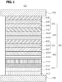
- FIG. 2 is a schematic cross-sectional view of an organic light emitting diode according to a second embodiment of the present invention.
- the organic light emitting diode D2 which includes two emitting parts, includes a first electrode 180, a second electrode 184, an organic emitting layer 182 between the first and second electrodes 180 and 184 and including first and second emitting parts ST1 and ST2 and a charge generation layer (CGL) 330.
- CGL charge generation layer
- the first electrode 180 is the anode for injecting a hole and includes a high work function conductive material, e.g., ITO, IZO or ZnO.
- the second electrode 184 is the cathode for injecting an electron and includes a low work function conductive material, e.g., Al, Mg or Al-Mg alloy.
- the CGL 330 is positioned between the first and second emitting parts ST1 and ST2. Namely, the first emitting part ST1, the CGL 330 and the second emitting part ST2 are sequentially stacked on the first electrode 180. In other words, the first emitting part ST1 is positioned between the first electrode 180 and the CGL 330, and the second emitting part ST2 is positioned between the second electrode 184 and the CGL 330.
- the first emitting part ST1 may include an HIL 312, a first HTL 314, a first EML 316 and a first ETL 318 sequentially stacked on the first electrode 180.
- the HIL 312 and the first HTL 314 are positioned between the first electrode 180 and the first EML 316.
- the HIL 312 is positioned between the first electrode 180 and the first HTL 314, and the first HTL 314 is positioned between the HIL 312 and the first EML 316.
- the first ETL 318 is positioned between the first EML 316 and the CGL 330.
- the HIL 312 may include at least one selected from the group consisting of MTDATA, CuPc, TCTA, NPD, HATCN, TDAPB, PEDOT/PSS, F4TCNQ and N-(biphenyl-4-yl)-9,9-dimethyl-N-(4-(9-phenyl-9H-carbazole-3-yl)phenyl)-9H-fluorene-2am ine.
- the HIL 312 may have a thickness of about 1 to 150nm.
- the hole injection property may be improved with the thickness above 1nm, and an increase of the driving voltage resulting from an increase of the thickness of the HIL 312 may be prevented with the thickness below 150nm.
- the HIL 312 may be omitted according to the structure or property of the organic light emitting diode.
- the first HTL 314 may include at least one selected from a group consisting of TPD, TCTA, MTDATA, NPD and CBP, but it is not limited thereto.
- the first HTL 314 may have a single-layered structure or a multi-layered structure.
- the first HTL 314 may have a thickness of about 1 to 150nm.
- the hole transporting property may be improved with the thickness above 1nm, and an increase of the driving voltage resulting from an increase of the thickness of the first HTL 314 may be prevented with the thickness below 150nm.
- the first EML 316 may be a blue EML.
- the first EML 316 may be a red EML, a green EML or a yellow EML.
- the first EML 316 may be a blue EML, a dark blue EML or a sky blue EML.
- the first EML 316 may be a double-layered structure of the blue EML and the red EML, the blue EML and yellow-green EML, or the blue EML and the green EML.
- the first EML 316 may be a phosphorescent EML including a host, e.g., 4,4'-bis(carbazol-9-yl)biphenyl (CBP), and at least one dopant selected from the group consisting of bis(1-phenylisoquinoline)acetylacetonate iridium (PIQIr(acac), bis(1-phenylquinoline)acetylacetonate iridium(PQIr(acac) and tris(1-phenylquinoline)iridium(PQIr) and octaethylporphyrin platinum (PtOEP), but it is not limited thereto.
- the first EML 316 may be a fluorescent EML including PBD:Eu(DBM) 3 (Phen) or perylene.
- the first emitting part ST1 has an emission peak range of about 600 to 650nm.
- the first EML 216 may be a phosphorescent EML including a host, e.g., CBP, and a dopant of iridium complex, but it is not limited thereto.
- the first EML 316 may a fluorescent EML including tris(8-hydroxyquinolinato)aluminum (Alq 3 ).
- the first emitting part ST1 has an emission peak range of about 510 to 570nm.
- the first EML 316 may be a phosphorescent EML including a host, e.g., CBP, and a dopant of iridium complex, but it is not limited thereto.
- the first EML 316 may a fluorescent EML including spiro-DPVBi, Spiro-CBP, distyryl benzene (DSB), distyryl arene (DSA), PFO-based polymer or PPV-based polymer.
- the first EML 316 may be a sky blue EML or deep blue (dark blue) EML.
- the first emitting part ST1 has an emission peak range of about 440 to 480nm.
- the first emitting part ST1 may include two EMLs.
- the first emitting part ST1 may include the blue EML and the red EML.
- the first emitting part ST1 has an emission peak range of about 440 to 650nm.
- the first EML 316 may have a single-layered structure of the yellow-green EML or a double-layered structure of the yellow-green EML and the green EML.
- the first EML 316 may include at least one host selected from a group consisting of CBP and bis(2-methyl-8-quinolinolate)-4-(phenylphenolato)aluminium (BAlq) and a phosphorescent yellow-green dopant.
- the first emitting part ST1 has an emission peak range of about 510 to 590nm.
- the first emitting part ST1 When the first emitting part ST1 includes two EMLs of the yellow-green EML and the red EML to improve the emitting efficiency (red efficiency), the first emitting part ST1 has an emission peak range of about 510 to 650nm.
- the first ETL 318 may include an organic compound represented by Formula 1, and a metal, e.g., an alkali metal or an alkali earth metal, may be doped into the organic compound.
- a metal e.g., an alkali metal or an alkali earth metal
- the first ETL 318 may have a thickness of about 1 to 150nm.
- the electron transporting property may be improved with the thickness above 1nm, and an increase of the driving voltage resulting from an increase of the thickness of the first ETL 318 may be prevented with the thickness below 150nm.
- the second emitting part ST2 may include a second HTL 322, a second EML 324, a second ETL 326 and an EIL 328.
- the second HTL 322 is positioned between the CGL 330 and the second EML 324
- the second ETL 326 is positioned between the second EML 324 and the second electrode 184.
- the EIL 328 is positioned between the second ETL 326 and the second electrode 184.
- the second HTL 322 and the second ETL 326 may be same as or different from the first HTL 314 and the first ETL 318 in the first emitting part ST1, respectively.
- the EIL 328 may be omitted according to the structure or property of the organic light emitting diode.
- the second EML 324 may be red, green, blue or yellow-green EML.
- the second EML 324 may be yellow-green EML.
- the first EML 316 may be the yellow-green EML
- the second EML 324 may be the blue EML.
- the second EML 324 may have a single-layered structure of the yellow-green EML or a double-layered structure of the yellow-green EML and the green EML.
- the single-layered second EML 324 may include at least one host selected from a group consisting of CBP and bis(2-methyl-8-quinolinolate)-4-(phenylphenolato)aluminium (BAlq) and a phosphorescent yellow-green dopant, but it is not limited thereto.
- the second ETL 326 may include an organic compound represented by Formula 1, and a metal, e.g., an alkali metal or an alkali earth metal, may be doped into the organic compound.
- a metal e.g., an alkali metal or an alkali earth metal
- the second ETL 326 may have a thickness of about 1 to 150nm.
- the electron transporting property may be improved with the thickness above 1nm, and an increase of the driving voltage resulting from an increase of the thickness of the second ETL 326 may be prevented with the thickness below 150nm.
- the EIL 328 may include an alkali halide material, e.g., LiF, NaF, KF, RbF, CsF, FrF, BeF 2 , MgF 2 , CaF 2 , SrF 2 , BaF 2 or RaF 2 , or an organic material, e.g., lithium quinolate (Liq), lithium benzoate, sodium stearate, tris-(8-hydroxyquinoline aluminum (Alq3), bis(8-hydroxy-2-methylquinoline)-4(4-phenylphenoxy)aluminum (BAlq), 2-biphenyl-4-yl-5-(4-t-butylphenyl)-1,3,4-oxadiazole (PBD), spiro-PBD or 3-(biphenyl-4-yl)-5-(4-tertbutylphenyl)-4-phenyl-4H-1,2,4-triazole (TAZ), but it
- the EIL 328 may include the organic compound of the present invention.
- the EIL 328 may further include a metal, e.g., an alkali metal or an alkali earth metal.
- the metal as a dopant in the EIL 328 may have a weight % of about 1 to about 30 with respect to the organic compound, but it is not limited thereto.
- the EIL 328 may have a thickness of about 1 to 50nm.
- the electron injection property may be improved with the thickness above 1nm, and an increase of the driving voltage resulting from an increase of the thickness of the EIL 328 may be prevented with the thickness below 50nm.
- the CGL 330 is positioned between the first emitting part ST1 and the second emitting part ST2. Namely, the first and second emitting parts ST1 and ST2 are connected by the CGL 330.
- the CGL 330 may be a P-N junction type CGL including an N-type CGL 330N and a P-type CGL 330P.
- the N-type CGL 330N is positioned between the first ETL 318 and the second HTL 322, and the P-type CGL 330P is positioned between the N-type CGL 330N and the second HTL 322.
- the CGL 330 generates a charge or separates a charge into a hole and an electron such that the hole and the electron are provided into the first and second emitting parts ST1 and ST2.
- the N-type CGL 330N provides the electron into the first ETL 318 of the first emitting part ST1, and the first ETL 318 provide the electron into the first EML 316 of the first emitting part ST1.
- the P-type CGL 330P provide the hole into the second HTL 322 of the second emitting part ST2, and the second HTL 322 provide the hole into the second EML 324 of the second emitting part ST2.
- the P-type CGL may include an organic material and a dopant, e.g., a metal or a p-type dopant.
- a dopant e.g., a metal or a p-type dopant.
- the metal as the dopant may be selected from the group consisting of Al, Cu, Fe, Pb, Zn, Au, Pt, W, In, Mo, Ni, Ti and their alloy.
- the generally known materials may be used as the p-type dopant and the organic material.
- the p-type dopant may be selected from the group consisting of F 4 -TCNQ, iodine, FeCl 3 , FeF 3 and SbCl 5
- the organic material may be selected from the group consisting of NPB, TPD, N,N,N' ,N' -tetranaphthalenyl-benzidine (TNB) and HAT-CN.
- the driving voltage is increased because of a lowest unoccupied molecular orbital (LUMO) energy level difference between each of the first ETL 318 and the N-type CGL 330N.
- LUMO lowest unoccupied molecular orbital
- At least one of the first ETL 318 and the N-type CGL 330N includes an organic compound represented in Formula 1 (or Formula 2).
- each of the first ETL 318 and the N-type CGL 330N may further include alkali metal or alkali earth metal as a dopant.
- the electron transporting/injection property may be further improved.
- the organic compound is combined or bonded with the alkali metal or the alkali earth metal in the N-type CGL 330 to form a gap state.
- the energy difference between the N-type CGL 330N and the P-type CGL 330P is decreased such that an electron transporting/injection property from the N-type CGL 330N into the first ETL 318 is improved.
- the alkali metal or the alkali earth metal may have a weight % of about 1 to 30 with respect to the organic compound, but it is not limited thereto.
- an alkali halide material e.g., LiF, NaF, KF, RbF, CsF, FrF, BeF 2 , MgF 2 , CaF 2 , SrF 2 , BaF 2 or RaF 2 , may be doped.
- the organic compound of the present invention includes the phenanthroline core, which has the nitrogen atom of a relatively electron rich sp 2 hybrid orbital, and the phosphine oxide moiety, which has excellent electron transporting property and excellent thermal stability, the electron transporting property of the organic compound of the present invention is improved.
- the charge generated in the N-type CGL is efficiently transported into the first ETL 318.
- the nitrogen atom of the phenanthroline core in the organic compound is combined or bonded with the alkali metal or the alkali earth metal as a dopant in the N-type CGL to form a gap state, the electron transporting property of the N-type CGL into the first ETL is further improved.
- the organic compound is combined with the alkali metal or the alkali earth metal in the N-type CGL, the diffusion of the alkali metal or the alkali earth metal into the P-type CGL is prevented.
- the organic compound when used in the N-type CGL in a tandem structure light emitting diode or OLED device, the electron is efficiently transferred from the N-type CGL into the first ETL, the driving voltage is reduced, and the lifetime and the emitting efficiency are improved.
- FIG. 3 is a schematic cross-sectional view of an organic light emitting diode according to a third embodiment of the present invention.
- an organic light emitting diode D3 includes a first electrode 180, a second electrode 184, an organic emitting layer 182 between the first and second electrodes 180 and 184 and including first to third emitting parts ST1, ST2 and ST3 and first and second CGLs 430 and 450.
- first to third emitting parts ST1, ST2 and ST3 and first and second CGLs 430 and 450 may be disposed between the first and second electrodes 180 and 184.
- the first electrode 180 is the anode for injecting a hole and includes a high work function conductive material, e.g., ITO, IZO or ZnO.
- the second electrode 184 is the cathode for injecting an electron and includes a low work function conductive material, e.g., Al, Mg or Al-Mg alloy.
- the first and second CGLs 430 and 450 are positioned between the first and second emitting parts ST1 and ST2 and the second and third emitting parts ST2 and ST3, respectively. Namely, the first emitting part ST1, the first CGL 430, the second emitting part ST2, the second CGL 450 and the third emitting part ST3 are sequentially stacked on the first electrode 180. In other words, the first emitting part ST1 is positioned between the first electrode 180 and the first CGL 430, and the second emitting part ST2 is positioned between the First and Second CGLs 430 and 450. In addition, the third emitting part ST3 is positioned between the second electrode 184 and the second CGL 450.
- the first emitting part ST1 may include an HIL 412, a first HTL 414, a first EML 416 and a first ETL 418 sequentially stacked on the first electrode 180.
- the HIL 412 and the first HTL 414 are positioned between the first electrode 180 and the first EML 416
- the HIL 412 is positioned between the first electrode 180 and the first HTL 414.
- the first ETL 418 is positioned between the first EML 416 and the first CGL 430.
- the HIL 412, the first HTL 414, the first EML 416 and the first ETL 418 may have substantially the same property and structure as those in FIG. 2 .
- the first EML 416 may be a blue EML such that the first emitting part ST1 may have an emission peak range of about 440 to 480nm.
- the second emitting part ST2 may include a second HTL 422, a second EML 424 and a second ETL 426.
- the second HTL 422 is positioned between the first CGL 430 and the second EML 424
- the second ETL 426 is positioned between the second EML 424 and the second CGL 450.
- the second HTL 422, second EML 424 and the second ETL 426 may have substantially the same property and structure as those in FIG. 2 .
- the second EML 424 may be a yellow-green EML such that the second emitting part ST2 may have an emission peak range of about 510 to 590nm.
- the third emitting part ST3 may include a third HTL 442, a third EML 444, a third ETL 446 and an EIL 448.
- the third HTL 442 is positioned between the second CGL 450 and the third EML 444
- the third ETL 446 is positioned between the third EML 444 and the second electrode 184.
- the EIL 448 is positioned between the third ETL 446 and the second electrode 184.
- the third HTL 442, the third ETL 446 and the EIL 448 may have substantially the same property and structure as the second HTL 422, the second ETL 426 and the EIL 428 in FIG. 2 .
- the third EML 444 may have substantially the same property as the first EML 416 or the second EML 424.
- the third EML 444 may be a blue EML such that the third emitting part ST3 may have an emission peak range of about 440 to 480nm.
- the first CGL 430 is positioned between the first emitting part ST1 and the second emitting part ST2, and the second CGL 450 is positioned between the second emitting part ST2 and the third emitting part ST3.
- Each of the first and second CGLs 430 and 450 may be a P-N junction type CGL.
- the first CGL 430 includes an N-type CGL 430N and a P-type CGL 430P
- the second CGL 450 includes an N-type CGL 450N and a P-type CGL 450P.
- the N-type CGL 430N is positioned between the first ETL 418 and the second HTL 422, and the P-type CGL 430P is positioned between the N-type CGL 430N and the second HTL 422.
- the N-type CGL 450N is positioned between the second ETL 426 and the third HTL 442
- the P-type CGL 450P is positioned between the N-type CGL 450N and the third HTL 442.
- Each of the first and second CGLs 430 and 450 generates a charge or separates a charge into a hole and an electron such that the hole and the electron are provided into the first to third emitting parts ST1 to ST3.
- the N-type CGL 430N provides the electron into the first ETL 418 of the first emitting part ST1
- the P-type CGL 430P provide the hole into the second HTL 422 of the second emitting part ST2.
- the N-type CGL 450N provides the electron into the second ETL 426 of the second emitting part ST2
- the P-type CGL 450P provide the hole into the third HTL 442 of the third emitting part ST3.
- Each of the P-type CGLs 430P and 450P may include an organic material and a dopant, e.g., a metal or a p-type dopant.
- a dopant e.g., a metal or a p-type dopant.
- the metal as the dopant may be selected from the group consisting of Al, Cu, Fe, Pb, Zn, Au, Pt, W, In, Mo, Ni, Ti and their alloy.
- the generally known materials may be used as the p-type dopant and the organic material.
- the p-type dopant may be selected from the group consisting of F 4 -TCNQ, iodine, FeCl 3 , FeF 3 and SbCl 5
- the organic material may be selected from the group consisting of NPB, TPD, N,N,N' ,N' -tetranaphthalenyl-benzidine (TNB) and HAT-CN.
- the driving voltage is increased because of a lowest unoccupied molecular orbital (LUMO) energy level difference between each of the first and second ETLs 418 and 426 and each of the N-type CGLs 430N and 450N.
- LUMO lowest unoccupied molecular orbital
- At least one of the first and second ETLs 418 and 426 and the N-type CGLs 430N and 450N includes an organic compound represented in Formula 1 (or Formula 2).
- each of the first and second ETLs 418 and 426 and the N-type CGLs 430N and 450N may further include alkali metal or alkali earth metal as a dopant.
- the alkali metal or the alkali earth metal may have a weight % of about 1 to 30 with respect to the organic compound, but it is not limited thereto.
- an alkali halide material e.g., LiF, NaF, KF, RbF, CsF, FrF, BeF 2 , MgF 2 , CaF 2 , SrF 2 , BaF 2 or RaF 2 , may be doped.
- the organic compound of the present invention includes the phenanthroline core, which has the nitrogen atom of a relatively electron rich sp 2 hybrid orbital, and the phosphine oxide moiety, which has excellent electron transporting property and excellent thermal stability, the electron transporting property of the organic compound of the present invention is improved. Accordingly, the charge generated in the N-type CGLs is efficiently transported into the ETLs.
- the nitrogen atom of the phenanthroline core in the organic compound is combined or bonded with the alkali metal or the alkali earth metal as a dopant in the N-type CGLs to form a gap state, the electron transporting property of the N-type CGLs into the ETLs is further improved.
- the organic compound is combined with the alkali metal or the alkali earth metal in the N-type CGLs, the diffusion of the alkali metal or the alkali earth metal into the P-type CGLs is prevented.
- the organic compound when used in the N-type CGLs in a tandem structure light emitting diode or OLED device, the electron is efficiently transferred from the N-type CGLs into the ETLs, the driving voltage is reduced, and the lifetime and the emitting efficiency are improved.
- FIG. 4 is a schematic cross-sectional view of an OLED device according to the present invention.
- an OLED device 100 includes a substrate 110, an organic light emitting diode D over the substrate 110, an encapsulation film 120 covering the organic light emitting diode D.
- a driving thin film transistor (TFT) Td is disposed on the substrate 110, and the organic light emitting diode D is connected to the driving TFT Td.
- a gate line and a data line are disposed on or over the substrate 110 and cross each other to define a pixel region.
- a power line which is parallel to and spaced apart from the gate line or the data line
- a switching TFT which is electrically connected to the gate line and the data line
- a storage capacitor which is connected to the power line and an electrode of the switching TFT may be formed on or over the substrate 110.
- the driving TFT Td is connected to the switching TFT and includes a semiconductor layer 152, a gate electrode 160, a source electrode 170 and a drain electrode 172.
- the semiconductor layer 152 is formed on the substrate 110.
- the semiconductor layer 152 may be formed of an oxide semiconductor material or a poly-silicon.
- a light-shielding pattern (not shown) may be formed under the semiconductor layer 152.
- the light to the semiconductor layer 152 is shielded or blocked by the light-shielding pattern such that thermal degradation of the semiconductor layer 152 can be prevented.
- impurities may be doped into both sides of the semiconductor layer 152.
- a gate insulating layer 154 is formed on the semiconductor layer 152.
- the gate insulating layer 154 may be formed of an inorganic insulating material such as silicon oxide or silicon nitride.
- the gate electrode 160 which is formed of a conductive material, e.g., metal, is formed on the gate insulating layer 154 to correspond to a center of the semiconductor layer 152.
- the gate electrode 160 is connected to the switching TFT.
- An interlayer insulating layer 162 which is formed of an insulating material, is formed on an entire surface of the substrate 110 including the gate electrode 160.
- the interlayer insulating layer 162 may be formed of an inorganic insulating material, e.g., silicon oxide or silicon nitride, or an organic insulating material, e.g., benzocyclobutene or photo-acryl.
- the interlayer insulating layer 162 includes first and second contact holes 164 and 166 exposing both sides of the semiconductor layer 152.
- the first and second contact holes 164 and 166 are positioned at both sides of the gate electrode 160 to be spaced apart from the gate electrode 160.
- the source electrode 170 and the drain electrode 172 which are formed of a conductive material, e.g., metal, are formed on the interlayer insulating layer 162.
- the source electrode 170 and the drain electrode 172 are spaced apart from each other with respect to the gate electrode 160 and respectively contact both sides of the semiconductor layer 152 through the first and second contact holes 164 and 166.
- the source electrode 170 is connected to the power line.
- the gate electrode 160, the source electrode 170 and the drain electrode 172 are positioned over the semiconductor layer 152. Namely, the driving TFT Td has a coplanar structure.
- the gate electrode may be positioned under the semiconductor layer, and the source and drain electrodes may be positioned over the semiconductor layer such that the driving TFT Td may have an inverted staggered structure.
- the semiconductor layer may include amorphous silicon.
- the switching TFT may have substantially the same structure as the driving TFT Td.
- the OLED device 100 may further include a color filter 190.
- the color filter 190 absorbs a part of the red, green and blue light.
- a red color filter pattern, a green color filer pattern and a blue color filter pattern may be disposed in each pixel region. Due to the color filter pattern 190, the OLED device 100 provides a full-color image.
- the color filter 190 is positioned between the organic light emitting diode D and the interlayer insulating layer 162 (or the substrate 110).
- the OLED device 100 is the bottom-emission type.
- the color filter 190 may be positioned on or over the organic light emitting diode D, e.g., over the second electrode 184.
- the color filter 190 may have a thickness of about 2 to 5 micrometers.
- the color filter 190 may be used with the tandem structure white organic light emitting diode D in FIG. 2 or FIG. 3 .
- a passivation layer 174 which includes a drain contact hole 176 exposing the drain electrode 172 of the driving TFT Td, is formed to cover the driving TFT Td and the color filter 190.
- a first electrode 180 which is connected to the drain electrode 172 of the driving TFT Td through the drain contact hole 176, is separately formed on the passivation layer 174 in each pixel region.
- the first electrode 180 may be an anode and may be formed of a conductive material having a relatively high work function.
- the first electrode 180 may be formed of a transparent conductive material such as ITO, IZO or ZnO.
- a reflection electrode or a reflection layer may be formed under the first electrode 180.
- the reflection electrode or the reflection layer may be formed of aluminum (Al), silver (Ag), nickel (Ni) or aluminum-palladium-copper (APC) alloy.
- a bank layer 186 which covers edges of the first electrode 180, is formed on the passivation layer 174.
- the bank 186 exposes a center of the first electrode 180 in the pixel region.
- An organic emitting layer 182 is formed on the first electrode 180. As explained below, the organic emitting layer includes a single emitting part or at least two emitting parts (the tandem structure).
- a second electrode 184 is formed over the substrate 110 including the emitting layer 182.
- the second electrode 184 is positioned at an entire surface of the display area.
- the second electrode 184 may be a cathode and may be formed of a conductive material having a relatively low work function.
- the second electrode 184 may be formed of Al, Mg or Al-Mg alloy.
- the first electrode 180, the emitting layer 182 and the second electrode 184 constitute the organic light emitting diode D.
- the encapsulation film 120 is formed on the organic light emitting diode D to prevent penetration of moisture into the organic light emitting diode D.
- the encapsulation film 120 may has a triple-layered structure of a first inorganic layer, an organic layer and a second inorganic layer. However, it is not limited thereto.
- the organic compound of the present invention includes the phenanthroline core, which has the nitrogen atom of a relatively electron rich sp 2 hybrid orbital, and the phosphine oxide moiety, which has excellent electron transporting property and excellent thermal stability, the electron transporting/injection property of the organic compound of the present invention is improved. Accordingly, when the ETL includes the organic compound, the electron is efficiently transported or injected into the EML. As a result, in the organic light emitting diode and/or the OLED device, the driving voltage is reduced, and the lifetime and the emitting efficiency are improved.
- the nitrogen atom of the phenanthroline core in the organic compound is combined or bonded with the alkali metal or the alkali earth metal as a dopant in the N-type CGL to form a gap state, the electron transporting property of the N-type CGL into the ETL is further improved.
- the organic compound is combined with the alkali metal or the alkali earth metal in the N-type CGL, the diffusion of the alkali metal or the alkali earth metal into the P-type CGL is prevented.
- the organic compound when used in the N-type CGL in a tandem structure light emitting diode or OLED device, the electron is efficiently transferred from the N-type CGL into the first ETL, the driving voltage is reduced, and the lifetime and the emitting efficiency are improved.
- the mixture was filtered under the reduced pressure and separated by a column chromatography using methylene chloride (MC) and hexane as an eluent.
- MC methylene chloride
- the resultant was crystallized using MC such that the compound of 2-(10-(4-(diphenylphosphine oxide)phenyl)anthracen-9-yl)-1,10-phenanthroline (10g, yield 70%) was obtained.
- the mixture was filtered under the reduced pressure and separated by a column chromatography using methylene chloride (MC) and hexane as an eluent.
- MC methylene chloride
- the resultant was crystallized using MC such that the compound of 2-(1-(4-(diphenylphosphineoxide)phenyl)naphthalene-4-yl)-1,10-phenanthroline (10g, yield 60%) was obtained.
- An ITO layer is deposited and patterned on a substrate and washed to form the anode (2mm*2mm).
- the substrate is loaded in a vacuum chamber having a base pressure of 5 ⁇ 7*10 -8 , and layers are sequentially deposited as below.
- the compound bathophenanthroline (Bphen) is used at the N-type CGL.
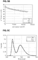
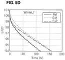
- the driving voltage, the emitting efficiency (cd/A), the external quantum efficiency (EQE), the color coordinate and the lifetime (T95 W) of the organic light emitting diodes of "Comparative Example” and “Example 1" and “Example 2” are measured and listed in Table 1.
- the current density, the emitting efficiency, the intensity and the lifetime are shown in FIGs. 5A to 5D .
- Table 1 Volt [V] Cd/A EQE [%] CIEx CIEy T95 W Ref 7.3 63.3 26.3 0.324 0.338 85.52 Ex1 7.0 65.2 27.5 0.319 0.329 122.08 Ex2 7.0 66.5 28.0 0.318 0.328 122.07
- the organic compound of the present invention since the organic compound of the present invention includes the phenanthroline core, which has the nitrogen atom of a relatively electron rich sp 2 hybrid orbital, and the phosphine oxide moiety, which has excellent electron transporting property and excellent thermal stability, the electron transporting property of the organic compound of the present invention is improved. Accordingly, when the organic compound is used in the ETL and/or the N-type CGL of the organic light emitting diode and the OLED device, the driving voltage is reduced, and the lifetime and the emitting efficiency are improved.
- the nitrogen atom of the phenanthroline core in the organic compound is combined or bonded with the alkali metal or the alkali earth metal as a dopant in the ETL or an N-type charge generation layer (CGL) to form a gap state, the electron transporting property of the ETL or the N-type CGL is further improved.
- the organic compound is combined with the alkali metal or the alkali earth metal in the ETL or the N-type CGL, the diffusion of the alkali metal or the alkali earth metal into the EML or the P-type CGL is prevented.
- the organic compound when used in the N-type CGL in a tandem structure light emitting diode or OLED device, the electron is efficiently transferred from the N-type CGL into the ETL, the driving voltage is reduced, and the lifetime and the emitting efficiency are improved.
- the invention is directed to following aspects.
Landscapes
- Chemical & Material Sciences (AREA)
- Physics & Mathematics (AREA)
- Engineering & Computer Science (AREA)
- Organic Chemistry (AREA)
- Materials Engineering (AREA)
- Spectroscopy & Molecular Physics (AREA)
- Optics & Photonics (AREA)
- Microelectronics & Electronic Packaging (AREA)
- General Health & Medical Sciences (AREA)
- Molecular Biology (AREA)
- Health & Medical Sciences (AREA)
- Biochemistry (AREA)
- Life Sciences & Earth Sciences (AREA)
- Geometry (AREA)
- Electroluminescent Light Sources (AREA)
Abstract
Description
- The present invention relates to an organic compound and more particularly to an organic compound being capable of reducing a driving voltage of an organic light emitting diode and improving an emitting efficiency and a lifetime of the organic light emitting diode and the organic light emitting display device including the organic compound.
- Recently, as requirements of a flat panel display device having small occupied area have been increased, an organic light emitting display (OLED) device including an organic light emitting diode are technically developed.
- The organic light emitting diode emits light by injecting electrons from a cathode as an electron injection electrode and holes from an anode as a hole injection electrode into an emitting material layer (EML), combining the electrons with the holes, generating an exciton, and transforming the exciton from an excited state to a ground state. A flexible substrate, for example, a plastic substrate, can be used as a base substrate where elements are formed. Since the OLED device does not require a backlight assembly, the OLED device has low weight and low power consumption. Moreover, the OLED device can be operated at a voltage (e.g., 10V or below) lower than a voltage required to operate other display devices.
- To efficiently inject the electron from the cathode into the EML, an organic light emitting diode for the OLED device may further include an electron injection layer (EIL) and an electron transporting layer (ETL) between the cathode and the EML. For example, the ETL may include tris-8-hydroxyquinoline aluminum (Alq3),
- 2-biphenyl-4-yl-5-(4-t-butylphenyl)-1,3,4-oxadiazole (PBD) or lithium quinolate (Liq). In addition, to increase the electron transfer from the EIL into the ETL, the ETL may further include an alkali metal or an alkali earth metal as a dopant.
- When the organic light emitting diode is driven, the alkali metal or the alkali earth metal may be transferred into an interface of the EML with the electron. Accordingly, an amount of the alkali metal or the alkali earth metal in the interface of the EML is increased, and an amount of the alkali metal or the alkali earth metal in the interface of the ETL is decreased. As a result, the electron injected to the EML is decreased such that the driving voltage of the organic light emitting diode is increased and the emitting efficiency of the organic light emitting diode is decreased. In addition, the lifetime of the organic light emitting diode is decreased.
- Accordingly, the present invention is directed to an organic compound and an organic light emitting diode and an organic light emitting display (OLED) device including the same that substantially obviate one or more of the problems due to limitations and disadvantages of the related art.
- An object of the present invention is to provide an organic compound being capable of preventing the decrease of an electron transporting/injection property and the lifetime.
- An object of the present invention is to provide an organic light emitting diode and an OLED device having improved electron transporting/injection property and lifetime.
- The objectives and other advantages of the invention will be realized and attained by the structure particularly pointed out in the written description and claims hereof as well as the appended drawings.
- To achieve these and other advantages and in accordance with the purpose of the present invention, as embodied and broadly described herein, an organic compound is represented by following Formula:

- In another aspect, an organic light emitting diode comprises the organic compound of the present invention.
- In one embodiment, the organic light emitting diode further comprising first and second electrodes facing each other; an emitting material layer between the first and second electrodes; and an electron transporting layer between the emitting material layer and the second electrode.
- In a further embodiment, the organic light emitting diode further comprises:
- first and second electrodes facing each other;
- a first emitting part between the first and second electrodes and including a first emitting material layer and a first electron transporting layer;
- a second emitting part between the first emitting part and the second electrode and including a second emitting material layer and a second electron transporting layer; and
- a first charge generation layer between the first and second emitting parts,
- wherein the organic compound according to the invention is included in at least one of the first electron transporting layer, the second electron transporting layer and the first charge generation layer.
- In another aspect, an organic light emitting display device comprises a substrate; the organic light emitting diode of the present invention; and a thin film transistor between the substrate and the organic light emitting diode and connected to the organic light emitting diode.
- In a further aspect, the invention is directed to the use of the organic compound of the present invention in an organic light emitting diode or an organic light emitting display device.
- The accompanying drawings, which are included to provide a further understanding of the invention and are incorporated in and constitute a part of this specification, illustrate embodiments of the invention and together with the description serve to explain the principles of the invention.
-
FIG. 1 is a schematic cross-sectional view of an organic light emitting diode according to a first embodiment of the present invention. -
FIG. 2 is a schematic cross-sectional view of an organic light emitting diode according to a second embodiment of the present invention. -
FIG. 3 is a schematic cross-sectional view of an organic light emitting diode according to a third embodiment of the present invention. -
FIG. 4 is a schematic cross-sectional view of an OLED device according to the present invention. -
FIGs. 5A to 5D are graphs showing emitting properties of an organic light emitting diode including an organic compound in an N-type CGL. - Reference will now be made in detail to the preferred embodiments, examples of which are illustrated in the accompanying drawings.
- An organic compound of the present invention includes a phenanthroline core and a phosphine oxide moiety directly or indirectly connected (or linked) to the phenanthroline core. The organic compound is represented in Formula 1.

- In the Formula 1, each of R1 to R3 is independently selected from the group consisting of hydrogen, deuterium, tritium, substituted or non-substituted C1-C20 alkyl, substituted or non-substituted C1-C20 alkoxy, substituted or non-substituted C5-C30 cycloalkyl, substituted or non-substituted C4-C30 heterocycloalkyl, substituted or non-substituted C5-C30 aryl, substituted or non-substituted C4-C30 heteroaryl, substituted or non-substituted C5-C30 oxyaryl and substituted or non-substituted C4-C30 hetero-oxyaryl. In the Formula 1, "a" is 2 or 3, "b" is 1 or 2, "c" is 2 or 3, and the summation of "a", "b" and "c" is 7. (a+b+c=7). Since "a" is 2 or 3, also the number of groups R1 is 2 or 3. In that case, the groups R1 can be selected independently of each other, i.e. they can be all identical, all different or two identical and one different (for a is 3). The same applies to R2 and R3. Ar1 is selected from the group consisting of substituted or non-substituted C1-C20 alkylene, substituted or non-substituted C5-C30 cycloalkylene, substituted or non-substituted C4-C30 heterocycloakylene, substituted or non-substituted C5-C30 arylene and substituted or non-substituted C4-C30 heteroarylene. "n" is 0, 1 or 2. Preferably, "n" is 1 or 2. More preferably, "n" is 2. Each of Ar2 and Ar3 is independently selected from the group consisting of hydrogen, deuterium, tritium, halogen, nitrile, substituted or non-substituted C5-C30 aryl, substituted or non-substituted C4-C30 heteroaryl, substituted or non-substituted C5-C30 oxyaryl and substituted or non-substituted C4-C30 hetero-oxyaryl.
- Preferably, in the Formula 1, "a" is 3, "b" is 2, "c" is 2.
- When R1 to R3 and Ar1 to Ar3 are substituted, the substituent may be one of non-substituted or halogen-substituted C1-C20 alkyl, non-substituted or halogen-substituted C1-C20 alkoxy, halogen, cyano, carboxyl, carbonyl, amine, C1-C20 alkyl amine, nitro, hydrazyl, sulfone, C1-C20 alkyl silyl, C1-C20 alkoxy silyl, C3-C30 cycloalkyl silyl, C5-C30 aryl silyl, substituted or non-substituted C5-C30 aryl and C4-C30 heteroaryl, but it is not limited thereto.
- The term of "hetero", which is used in heteroaryl, heteroarylene, and so on, means that at least one carbon atom in the aromatic ring or alicyclic ring is substituted by a heteroatom being selected from the group consisting of nitrogen atom (N), oxygen atom (O) and sulfur atom (S).
- For example, each of R1 to R3 may be substituted or non-substituted C5-C30 aryl or substituted or non-substituted C4-C30 heteroaryl. Each of R1 to R3 may be fused or non-fused homo-aromatic ring, such as phenyl, biphenyl, terphenyl, tetraphenyl, naphtyl, anthracenyl, indenyl, phenanthrenyl, azulenyl, pyrenyl, fluorenyl, tetracenyl, indacenyl or spiro-fluorenyl, or fused or non-fused hetero-aromatic ring, such as pyrrolyl, pyridyl (or pyridinyl), pyrimidyl (pyrimidinyl), pyrazinyl, pyridazinyl, triazinyl, tetrazinyl, imidazolyl, pyrazolyl, indolyl, carbazolyl, benzocarbazolyl, dibenzocarbazolyl, carbolinyl, indolocarbazolyl, indenocarbazolyl, quinolinyl, iso-quinolinyl, phthalazinyl, quinoxalinyl, cinnolinyl, quinazolinyl, benzoquinolinyl, benzo iso-quinolinyl, benzoqhinazolinyl, benzoquinoxalinyl, acrydinyl, phenanthrolinyl, furanyl, pyranyl, oxazinyl, oxazolyl, oxadiazolyl, triazolyl, dioxynyl, benzofuranyl, dibenzofuranyl, thio-pyranyl, thiazinyl, thiophenyl or N-substituted spiro-fluorenyl.
- For example, each of R1 to R3 may be independently selected from the group consisting of phenyl, alkylphenyl, biphenyl, alkylbiphenyl, halophenyl, alkoxyphenyl, haloalkoxyphenyl, cyanophenyl, silylphenyl, naphthyl, alkylnaphthyl, halonaphthyl, cyanonaphthyl, silylnaphthyl, phenylnaphthyl, pyridyl, alkylpyridyl, halopyridyl, cyanopyridyl, alkoxypyridyl, silylpyridyl, phenylpyridyl, pyrimidyl, halopyrimidyl, cyanopyrimidyl, alkoxypyrimidyl, phenylpyrimidyl, quinolinyl, isoquinolinyl, phenylquinolinyl, quinoxalinyl, pyrazinyl, quinazolinyl, naphthyridinyl, benzothiophenyl, benzofuranyl, dibenzothiophenyl, arylthiazolyl, dibenzofuranyl, fluorenyl, carbazoyl, imidazolyl, carbolinyl, phenanthrenyl, terphenyl, terpyridyl, phenylterpyridyl, triphenylenyl, fluoranthenyl and diazafluorenyl. Preferably, each of R1 to R3 is independently selected from hydrogen, substituted or non-substituted phenyl, substituted or non-substituted pyridyl, substituted or non-substituted naphthyl. Preferably, R2 and R3 are hydrogen, andR1 is independently selected from hydrogen, substituted or non-substituted phenyl, substituted or non-substituted pyridyl, substituted or non-substituted naphthyl. For "a" is 3, the groups R1 are all identical or two are identical and one is different from the other two.
- The carrier mobility of the organic compound may be controlled by Ar1 as a linker (or connection moiety). Ar1 may be selected from C1-C20 alkylene, such as methylene, ethylene or butylene, substituted or non-substituted C5-C30 arylene and substituted or non-substituted C4-C30 heteroarylene.
- When Ar1 is substituted or non-substituted C5-C30 arylene or substituted or non-substituted C4-C30 heteroarylene, Ar1 may be selected from the group consisting of phenylene, biphenylene, terphenylene, triphenylene, tetraphenylene, indenylene, naphthylene, azulenylene, indacenylene, acenaphthylene, fluorenylene, dibenzofluorenylene, spiro-fluorenylene, phenalenylene, phenanthrenylene, anthracenylene, fluoranthrenylene, triphenylenylene, pyrenylene, chrysenylene, naphthacenylene, picenylene, perylenylene, pentaphenylene, hexacenylene, pyrrolylene, imidazolylene, benzimidazolylene, pyrazolylene, pyridinylene, terpyridinylene, pyrazinylene, pyrimidinylene, pyridazinylene, isoindolylene, indolylene, indazolylene, purinylene, quinolinylene, isoquinolinylene, benzoquinolinylene, phthalazinylene, naphthyridinylene, quinoxalinylene, quinazolinylene, benzoquinolinylene, benzo iso-quinolinylene, benzoquinazolinylene, benzoquinoxalinylene, cinnolinylene, phenanthridinylene, carbolinylene, acridinylene, phenanthrolinylene, phenazinylene, benzoxazolylene, benzimidazolylene, furanylene, benzofuranylene, thiophenylene, benzothiophenylene, dibenzothiophenylene, thiazolylene, isothiazolylene, benzothiazolylene, isoxazolylene, oxazolylene, triazolylene, tetrazolylene, oxadiazolylene, triazinylene, dibenzofuranylene, dibenzothiophenylene, carbazolylene, benzocarbazolylene, dibenzocarbazolylene, indolocarbazolylene, indenocarbazolylene, imidazopyrimidinylene and imidazopyridinylene.
- Preferably, Ar1 is selected from the group consisting of phenylene, biphenylene, terphenylene, naphthylene, anthracenylene, phenanthrenylene, triphenylene, pyrenylene, fluorenylene, pyridinylene, pyrimidinylene, pyridazinylene, pyrazinylene, benzothiophenylene, dibenzothiophenylene, benzofuranylene and dibenzofuranylene, which may be substituted by C1-C20 alkyl, cyano, C5-C30 aryl or C4-C30 heteroaryl. More preferably, Ar1 is selected from the group consisting of phenylene, naphthylene, anthracenylene, phenanthrenylene, pyrenylene, fluorenylene, pyridinylene, pyrimidinylene, pyrazinylene, benzothiophenylene, dibenzothiophenylene, benzofuranylene and dibenzofuranylene, which may be substituted by C1-C5 alkyl, C5-C30 aryl or C4-C30 heteroaryl.
- When the number of rings of Ar1 is increased, the conjugation length of the organic compound is increased such that the energy band gap of the organic compound is decreased. Accordingly, the number of rings of Ar1 may be 1 to 4. To improve the electron transporting property of the organic compound, Ar1 may be 5-numbered atom ring to 7-numbered atom ring, and beneficially 6-numbered atom ring.
- In the organic compound of the exemplary embodiment of the present invention, each of Ar2 and Ar3 may be independently selected from substituted or non-substituted C5-C30 aryl and substituted or non-substituted C4-C30 heteroaryl. For example, each of Ar2 and Ar3 may be fused or non-fused homo-aromatic ring, such as phenyl, biphenyl, terphenyl, tetraphenyl, naphtyl, anthracenyl, indenyl, phenanthrenyl, azulenyl, pyrenyl, fluorenyl, tetracenyl, indacenyl or spiro-fluorenyl, or fused or non-fused hetero-aromatic ring, such as pyrrolyl, pyridyl, pyrimidinyl, pyrazinyl, pyridazinyl, triazinyl, tetrazinyl, imidazolyl, pyrazolyl, indolyl, carbazolyl, benzocarbazolyl, dibenzocarbazolyl, carbolinyl, indolocarbazolyl, indenocarbazolyl, quinolinyl, iso-quinolinyl, phthalazinyl, quinoxalinyl, cinnolinyl, quinazolinyl, benzoquinolinyl, benzo iso-quinolinyl, benzoqhinazolinyl, benzoquinoxalinyl, acrydinyl, phenanthrolinyl, furanyl, pyranyl, oxazinyl, oxazolyl, oxadiazolyl, triazolyl, dioxynyl, benzofuranyl, dibenzofuranyl, thio-pyranyl, thiazinyl, thiophenyl or N-substituted spiro-fluorenyl, and beneficially phenyl, biphenyl, anthracenyl, pyridyl, pyrimidyl, pyrazinyl, pyridazinyl or carbazolyl.
- Preferably, each of Ar2 and Ar3 is independently selected from substituted or non-substituted phenyl, biphenyl, anthracenyl, pyridyl, pyrimidyl, pyrazinyl, pyridazinyl or carbazolyl. Preferably, in one embodiment in the compound of Formula 1 "a" is 3, "b" is 2, "c" is 2, R2 and R3 are hydrogen, at R1 is independently selected from hydrogen, substituted or non-substituted phenyl, substituted or non-substituted pyridyl, substituted or non-substituted naphthyl, wherein the groups R1 are all identical or two are identical and one is different from the other two, "n" is 1 or 2, Ar1 is selected from the group consisting of phenylene, biphenylene, terphenylene, naphthylene, anthracenylene, phenanthrenylene, triphenylene, pyrenylene, fluorenylene, pyridinylene, pyrimidinylene, pyridazinylene, pyrazinylene, benzothiophenylene, dibenzothiophenylene, benzofuranylene and dibenzofuranylene, which may be substituted by C1-C20 alkyl, cyano, C5-C30 aryl or C4-C30 heteroaryl, each of Ar2 and Ar3 is independently selected from substituted or non-substituted phenyl, biphenyl, anthracenyl, pyridyl, pyrimidyl, pyrazinyl, pyridazinyl or carbazolyl.
- Since the organic compound of the present invention includes the phenanthroline core, which has the nitrogen atom of a relatively electron rich sp2 hybrid orbital, and the phosphine oxide moiety, which has excellent electron transporting property and excellent thermal stability, the electron transporting property of the organic compound of the present invention is improved. Accordingly, when the organic compound is used in an ETL of the organic light emitting diode, and an OLED device, the driving voltage is reduced, and the lifetime and the emitting efficiency are improved.
- In addition, since the nitrogen atom of the phenanthroline core in the organic compound is combined or bonded with the alkali metal or the alkali earth metal as a dopant in the ETL or an N-type charge generation layer (CGL) to form a gap state, the electron transporting property of the ETL or the N-type CGL is further improved. Moreover, since the organic compound is combined with the alkali metal or the alkali earth metal in the ETL or the N-type CGL, the diffusion of the alkali metal or the alkali earth metal into the EML or the P-type CGL is prevented. Accordingly, when the organic compound is used in the N-type CGL in a tandem structure light emitting diode or OLED device, the electron is efficiently transferred from the N-type CGL into the ETL, the driving voltage is reduced, and the lifetime and the emitting efficiency are improved.
- Preferably, the organic compound in the Formula 1 is one of materials in Formula 2 below.


- Preferably, the organic compound in the Formula 1 is one of materials in Formula 2 below.


- Since the organic compound of the present invention includes the phenanthroline core having two nitrogen atoms, which have a rich electron property, and the phosphine oxide moiety, which has excellent electron transporting property and excellent thermal stability, the electron transporting property of the organic compound of the present invention is improved. In addition, since the phenanthroline core (or moiety) has excellent combination property to the p-type dopant, i.e., the alkali metal, in the ETL or N-type CGL, the carrier in the cathode or the N-type CGL is efficiently transported or injected into the EML or the ETL. For example, when the organic compound is used in the ETL of the organic light emitting diode and the OLED device, the electron is efficiently transferred from the cathode into the EML such that the driving voltage is reduced, and the lifetime and the emitting efficiency are improved. Moreover, since the organic compound is combined with the alkali metal or the alkali earth metal in the ETL or the N-type CGL, the diffusion of the alkali metal or the alkali earth metal into the EML or the P-type CGL is prevented. Further, since the nitrogen atom of the phenanthroline core in the organic compound is combined or bonded with the alkali metal or the alkali earth metal as a dopant in the ETL or an N-type charge generation layer (CGL) to form a gap state, the electron transporting property of the ETL or the N-type CGL is further improved.
- As mentioned above, in the organic compound of the present invention, the phosphine oxide moiety, which has excellent electron transporting property and thermal stability, and the phenanthroline core, which has nitrogen atoms, are connected to each other. Accordingly, the organic compound is used in a layer of the organic light emitting diode requiring the electron transporting property and/or the electron injection property.
-
FIG. 1 is a schematic cross-sectional view of an organic light emitting diode according to a first embodiment of the present invention. - As shown in
FIG. 1 , the organic light emitting diode D1 includes afirst electrode 180, asecond electrode 184, an organic emitting layer 182 (e.g., an organic material layer or an emitting part) between the first andsecond electrodes layer 182 includes a hole injection layer (HIL) 210, a hole transporting layer (HTL) 220, an emitting material layer (EML) 230, an electron transporting layer (ETL) 240 and an electron injection layer (EIL) 250 sequentially stacked on thefirst electrode 180. Namely, the organic light emitting diode D1 of the first embodiment of the present invention includes a single emitting part. - The
first electrode 180 is the anode for injecting a hole and includes a high work function conductive material, e.g., indium-tin-oxide (ITO), indium-zinc-oxide (IZO) or zinc oxide (ZnO). Thesecond electrode 184 is the cathode for injecting an electron and includes a low work function conductive material, e.g., aluminum (Al), magnesium (Mg) or Al-Mg alloy. TheHIL 210 is positioned between thefirst electrode 180 and theHTL 220. An interface property between thefirst electrode 180 of an inorganic material and theHTL 220 of an organic material is improved by theHIL 210. For example, theHIL 210 may include one of 4,4',4"-tris(3-methylphenylphenylamino)triphenylamine (MTDATA), copper phthalocyanine (CuPc), tris(4-carbazoyl-9-yl-phenyl)amine (TCTA), N,N'-diphenyl-N,N'-bis(1-naphthyl)-1,1'-biphenyl-4,4"-diamine (NPB or NPD), 1,4,5,8,9,1 1-hexaazatriphenylenehexacarbonitrile (HATCN), 1,3,5-tris[4-(diphenylamino)phenyl]benzene(TDAPB), poly(3,4-ethylenedioxythiphene)polystyrene sulfonate (PEDOT/PSS), 2,3,5,6-tetrafluoro-7,7,8,8-tetracyanoquinodimethane (F4TCNQ) and N-(biphenyl-4-yl)-9,9-dimethyl-N-(4-(9-phenyl-9H-carbazol-3-yl)phenyl)-9H-fluoren-2-ami ne. - The
HIL 210 may have a thickness of about 1 to 150nm. The hole injection property may be improved with the thickness above 1nm, and an increase of the driving voltage resulting from an increase of the thickness of theHIL 210 may be prevented with the thickness below 150nm. TheHIL 210 may be omitted. - The
HTL 220 is positioned between theHIL 210 and the EML 230. For example, theHTL 220 may include a hole transporting material such as - N,N'-diphenyl-N,N'-bis(3-methylphenyl)-1,1'-biphenyl-4,4'-diamine (TPD), MTDATA, TCTA, NPD or 4,4'-bis(N-carbazolyl)-1,1'-biphenyl (CBP). The
HIL 220 may have a double-layered structure of different hole transporting materials. - The
HTL 220 may have a thickness of about 1 to 150nm. The hole transporting property may be improved with the thickness above 1nm, and an increase of the driving voltage resulting from an increase of the thickness of theHTL 220 may be prevented with the thickness below 150nm. - The EML 230 may include a host and a dopant. For example, when the EML 230 emits the blue light, a fluorescent host, such as anthracene derivative, pyrene derivative or perylene derivative, and a fluorescent dopant are used in the EML 230.
- For example, the fluorescent host for the EML 230 may be selected from the group consisting of 4,4'-bis(2,2'-diphenylyinyl)-1,1'-biphenyl (DPVBi), 9,10-di-(2-naphtyl)anthracene (ADN), 2,5,8,11-tetra-t-butylperylene (TBADN), 2-tert-butyl-9,10-di(2-naphthyl)anthracene, 2-methyl-9,10-di(2-naphtyl)anthracene (MADN) and 2,2',2"-(1,3,5-benzinetriyl)-tris(1-phenyl-1-H-benzimidazole) (TBPi).
- For example, the fluorescent dopant for the EML 230 may be selected from the group consisting of 4,4'-bis(9-ethyl-3-carbazovinylene)-1,1'-biphenyl (BCzVBi), 2,5,8,11-tetra(tert-butyl)perylene (TBP) and diphenyl-[4-(2-[1,1;4,1]terphenyl-4-yl-vinyl)-phenyl]-amine (BD-1).
- When the EML 230 emits the green light or the red light, the EML 230 may include a phosphorescent host, e.g., carbazole derivative, and a phosphorescent dopant, e.g., a metal (iridium) complex. The dopant may have a weight % of about 1 to about 30 with respect to the host.
- The
ETL 240 is positioned between the EML 230 and thesecond electrode 184, and theEIL 250 is positioned between theETL 240 and thesecond electrode 184. - The
ETL 240 includes the organic compound of the present invention. In addition, theETL 240 may further include a metal, e.g., an alkali metal or an alkali earth metal. The metal as a dopant in theETL 240 may have a weight % of about 1 to about 30 with respect to the organic compound, but it is not limited thereto. For example, the alkali metal may include Li, Na, K and Cs, and the alkali earth metal may include Mg, Sr, Ba and Ra. But, it is not limited thereto. TheETL 240 may have a single-layered structure or multi-layered structure. - The
ETL 240 may have a thickness of about 1 to 150nm. The electron transporting property may be improved with the thickness above 1nm, and an increase of the driving voltage resulting from an increase of the thickness of theETL 240 may be prevented with the thickness below 150nm. - An electron injection is improved by the
EIL 250. TheEIL 250 may include an alkali halide material, e.g., LiF, NaF, KF, RbF, CsF, FrF, BeF2, MgF2, CaF2, SrF2, BaF2 or RaF2, or an organic material, e.g., lithium quinolate (Liq), lithium benzoate, sodium stearate, tris-(8-hydroxyquinoline aluminum (Alq3), bis(8-hydroxy-2-methylquinoline)-4(4-phenylphenoxy)aluminum (BAlq), 2-biphenyl-4-yl-5-(4-t-butylphenyl)-1,3,4-oxadiazole (PBD), spiro-PBD or 3-(biphenyl-4-yl)-5-(4-tertbutylphenyl)-4-phenyl-4H-1,2,4-triazole (TAZ), but it is not limited thereto. TheEIL 250 may be omitted. - Alternatively, the
EIL 250 may include the organic compound of the present invention. In addition, theEIL 250 may further include a metal, e.g., an alkali metal or an alkali earth metal. The metal as a dopant in theEIL 250 may have a weight % of about 1 to about 30 with respect to the organic compound, but it is not limited thereto. - The
EIL 250 may have a thickness of about 1 to 50nm. The electron injection property may be improved with the thickness above 1nm, and an increase of the driving voltage resulting from an increase of the thickness of theEIL 250 may be prevented with the thickness below 50nm. - Since the organic compound of the present invention includes the phenanthroline core, which has the nitrogen atom of a relatively electron rich sp2 hybrid orbital, and the phosphine oxide moiety, which has excellent electron transporting property and excellent thermal stability, the electron transporting property of the organic compound of the present invention is improved. Accordingly, when the organic compound is used in the ETL of the organic light emitting diode and the OLED device, the driving voltage is reduced, and the lifetime and the emitting efficiency are improved.
- On the other hand, the organic compound of the present invention may be applied to a tandem structure organic light emitting diode emitting the white light. The tandem structure white organic light emitting diode may be used in a lighting apparatus, a thin light source, a backlight unit of a liquid crystal display device and a full color display device including a color filter.
- In the white organic light emitting diode, properties of color purity and color stability as well as an emitting efficiency and a lifetime are important facts. For example, the white organic light emitting diode may be classified into a single-layered emission structure and a multi-layered emission structure. To provide the long lifetime white organic light emitting diode, the white organic light emitting diode having a stack structure of at least two emitting parts may be used. This structure may be referred to as the tandem structure.
-
FIG. 2 is a schematic cross-sectional view of an organic light emitting diode according to a second embodiment of the present invention. - As shown in
FIG. 2 , the organic light emitting diode D2, which includes two emitting parts, includes afirst electrode 180, asecond electrode 184, an organic emittinglayer 182 between the first andsecond electrodes - The
first electrode 180 is the anode for injecting a hole and includes a high work function conductive material, e.g., ITO, IZO or ZnO. Thesecond electrode 184 is the cathode for injecting an electron and includes a low work function conductive material, e.g., Al, Mg or Al-Mg alloy. - The
CGL 330 is positioned between the first and second emitting parts ST1 and ST2. Namely, the first emitting part ST1, theCGL 330 and the second emitting part ST2 are sequentially stacked on thefirst electrode 180. In other words, the first emitting part ST1 is positioned between thefirst electrode 180 and theCGL 330, and the second emitting part ST2 is positioned between thesecond electrode 184 and theCGL 330. - The first emitting part ST1 may include an
HIL 312, afirst HTL 314, afirst EML 316 and afirst ETL 318 sequentially stacked on thefirst electrode 180. Namely, theHIL 312 and thefirst HTL 314 are positioned between thefirst electrode 180 and thefirst EML 316. TheHIL 312 is positioned between thefirst electrode 180 and thefirst HTL 314, and thefirst HTL 314 is positioned between theHIL 312 and thefirst EML 316. In addition, thefirst ETL 318 is positioned between thefirst EML 316 and theCGL 330. - A hole injection from the
first electrode 180 into thefirst EML 316 is improved by theHIL 312. TheHIL 312 may include at least one selected from the group consisting of MTDATA, CuPc, TCTA, NPD, HATCN, TDAPB, PEDOT/PSS, F4TCNQ and N-(biphenyl-4-yl)-9,9-dimethyl-N-(4-(9-phenyl-9H-carbazole-3-yl)phenyl)-9H-fluorene-2am ine. - The
HIL 312 may have a thickness of about 1 to 150nm. The hole injection property may be improved with the thickness above 1nm, and an increase of the driving voltage resulting from an increase of the thickness of theHIL 312 may be prevented with the thickness below 150nm. TheHIL 312 may be omitted according to the structure or property of the organic light emitting diode. - A hole transporting is improved by the
first HTL 314. Thefirst HTL 314 may include at least one selected from a group consisting of TPD, TCTA, MTDATA, NPD and CBP, but it is not limited thereto. Thefirst HTL 314 may have a single-layered structure or a multi-layered structure. - The
first HTL 314 may have a thickness of about 1 to 150nm. The hole transporting property may be improved with the thickness above 1nm, and an increase of the driving voltage resulting from an increase of the thickness of thefirst HTL 314 may be prevented with the thickness below 150nm. - The
first EML 316 may be a blue EML. Alternatively, thefirst EML 316 may be a red EML, a green EML or a yellow EML. When thefirst EML 316 is the blue EML, thefirst EML 316 may be a blue EML, a dark blue EML or a sky blue EML. In addition, thefirst EML 316 may be a double-layered structure of the blue EML and the red EML, the blue EML and yellow-green EML, or the blue EML and the green EML. - When the
first EML 316 is the red EML, thefirst EML 316 may be a phosphorescent EML including a host, e.g., 4,4'-bis(carbazol-9-yl)biphenyl (CBP), and at least one dopant selected from the group consisting of bis(1-phenylisoquinoline)acetylacetonate iridium (PIQIr(acac), bis(1-phenylquinoline)acetylacetonate iridium(PQIr(acac) and tris(1-phenylquinoline)iridium(PQIr) and octaethylporphyrin platinum (PtOEP), but it is not limited thereto. Alternatively, thefirst EML 316 may be a fluorescent EML including PBD:Eu(DBM)3(Phen) or perylene. In this instance, the first emitting part ST1 has an emission peak range of about 600 to 650nm. - When the
first EML 316 is the green EML, the first EML 216 may be a phosphorescent EML including a host, e.g., CBP, and a dopant of iridium complex, but it is not limited thereto. Alternatively, thefirst EML 316 may a fluorescent EML including tris(8-hydroxyquinolinato)aluminum (Alq3). In this instance, the first emitting part ST1 has an emission peak range of about 510 to 570nm. - When the
first EML 316 is the blue EML, thefirst EML 316 may be a phosphorescent EML including a host, e.g., CBP, and a dopant of iridium complex, but it is not limited thereto. Alternatively, thefirst EML 316 may a fluorescent EML including spiro-DPVBi, Spiro-CBP, distyryl benzene (DSB), distyryl arene (DSA), PFO-based polymer or PPV-based polymer. As mentioned above, thefirst EML 316 may be a sky blue EML or deep blue (dark blue) EML. In this instance, the first emitting part ST1 has an emission peak range of about 440 to 480nm. - On the other hand, to improve the emitting efficiency (red efficiency), the first emitting part ST1 may include two EMLs. For example, the first emitting part ST1 may include the blue EML and the red EML. In this instance, the first emitting part ST1 has an emission peak range of about 440 to 650nm.
- In addition, the
first EML 316 may have a single-layered structure of the yellow-green EML or a double-layered structure of the yellow-green EML and the green EML. In this instance, thefirst EML 316 may include at least one host selected from a group consisting of CBP and bis(2-methyl-8-quinolinolate)-4-(phenylphenolato)aluminium (BAlq) and a phosphorescent yellow-green dopant. The first emitting part ST1 has an emission peak range of about 510 to 590nm. - When the first emitting part ST1 includes two EMLs of the yellow-green EML and the red EML to improve the emitting efficiency (red efficiency), the first emitting part ST1 has an emission peak range of about 510 to 650nm.
- An electron transporting is improved by the
first ETL 318. Thefirst ETL 318 may include an organic compound represented by Formula 1, and a metal, e.g., an alkali metal or an alkali earth metal, may be doped into the organic compound. - The
first ETL 318 may have a thickness of about 1 to 150nm. The electron transporting property may be improved with the thickness above 1nm, and an increase of the driving voltage resulting from an increase of the thickness of thefirst ETL 318 may be prevented with the thickness below 150nm. - The second emitting part ST2 may include a
second HTL 322, asecond EML 324, asecond ETL 326 and anEIL 328. Thesecond HTL 322 is positioned between theCGL 330 and thesecond EML 324, and thesecond ETL 326 is positioned between thesecond EML 324 and thesecond electrode 184. In addition, theEIL 328 is positioned between thesecond ETL 326 and thesecond electrode 184. - The
second HTL 322 and thesecond ETL 326 may be same as or different from thefirst HTL 314 and thefirst ETL 318 in the first emitting part ST1, respectively. TheEIL 328 may be omitted according to the structure or property of the organic light emitting diode. - The
second EML 324 may be red, green, blue or yellow-green EML. For example, when thefirst EML 316 is the blue EML, thesecond EML 324 may be yellow-green EML. Alternatively, thefirst EML 316 may be the yellow-green EML, and thesecond EML 324 may be the blue EML. - When the
second EML 324 is the yellow-green EML, thesecond EML 324 may have a single-layered structure of the yellow-green EML or a double-layered structure of the yellow-green EML and the green EML. - For example, the single-layered
second EML 324 may include at least one host selected from a group consisting of CBP and bis(2-methyl-8-quinolinolate)-4-(phenylphenolato)aluminium (BAlq) and a phosphorescent yellow-green dopant, but it is not limited thereto. - An electron transporting is improved by the
second ETL 326. Thesecond ETL 326 may include an organic compound represented by Formula 1, and a metal, e.g., an alkali metal or an alkali earth metal, may be doped into the organic compound. - The
second ETL 326 may have a thickness of about 1 to 150nm. The electron transporting property may be improved with the thickness above 1nm, and an increase of the driving voltage resulting from an increase of the thickness of thesecond ETL 326 may be prevented with the thickness below 150nm. - An electron injection is improved by the
EIL 328. TheEIL 328 may include an alkali halide material, e.g., LiF, NaF, KF, RbF, CsF, FrF, BeF2, MgF2, CaF2, SrF2, BaF2 or RaF2, or an organic material, e.g., lithium quinolate (Liq), lithium benzoate, sodium stearate, tris-(8-hydroxyquinoline aluminum (Alq3), bis(8-hydroxy-2-methylquinoline)-4(4-phenylphenoxy)aluminum (BAlq), 2-biphenyl-4-yl-5-(4-t-butylphenyl)-1,3,4-oxadiazole (PBD), spiro-PBD or 3-(biphenyl-4-yl)-5-(4-tertbutylphenyl)-4-phenyl-4H-1,2,4-triazole (TAZ), but it is not limited thereto. TheEIL 328 may be omitted. - Alternatively, the
EIL 328 may include the organic compound of the present invention. In addition, theEIL 328 may further include a metal, e.g., an alkali metal or an alkali earth metal. The metal as a dopant in theEIL 328 may have a weight % of about 1 to about 30 with respect to the organic compound, but it is not limited thereto. - The
EIL 328 may have a thickness of about 1 to 50nm. The electron injection property may be improved with the thickness above 1nm, and an increase of the driving voltage resulting from an increase of the thickness of theEIL 328 may be prevented with the thickness below 50nm. - In the tandem structure organic light emitting diode D2, to increase the current efficiency generating from each of the
EMLs CGL 330 is positioned between the first emitting part ST1 and the second emitting part ST2. Namely, the first and second emitting parts ST1 and ST2 are connected by theCGL 330. TheCGL 330 may be a P-N junction type CGL including an N-type CGL 330N and a P-type CGL 330P. - The N-type CGL 330N is positioned between the
first ETL 318 and thesecond HTL 322, and the P-type CGL 330P is positioned between the N-type CGL 330N and thesecond HTL 322. TheCGL 330 generates a charge or separates a charge into a hole and an electron such that the hole and the electron are provided into the first and second emitting parts ST1 and ST2. The N-type CGL 330N provides the electron into thefirst ETL 318 of the first emitting part ST1, and thefirst ETL 318 provide the electron into thefirst EML 316 of the first emitting part ST1. On the other hand, the P-type CGL 330P provide the hole into thesecond HTL 322 of the second emitting part ST2, and thesecond HTL 322 provide the hole into thesecond EML 324 of the second emitting part ST2. - The P-type CGL may include an organic material and a dopant, e.g., a metal or a p-type dopant. For example, the metal as the dopant may be selected from the group consisting of Al, Cu, Fe, Pb, Zn, Au, Pt, W, In, Mo, Ni, Ti and their alloy. In addition, the generally known materials may be used as the p-type dopant and the organic material. For example, the p-type dopant may be selected from the group consisting of F4-TCNQ, iodine, FeCl3, FeF3 and SbCl5, and the organic material may be selected from the group consisting of NPB, TPD, N,N,N' ,N' -tetranaphthalenyl-benzidine (TNB) and HAT-CN.
- In the tandem structure organic light emitting diode, when the electrons are transported from the N-type CGL 330N into the
first ETL 318, the driving voltage is increased because of a lowest unoccupied molecular orbital (LUMO) energy level difference between each of thefirst ETL 318 and the N-type CGL 330N. - To overcome the above problem, at least one of the
first ETL 318 and the N-type CGL 330N includes an organic compound represented in Formula 1 (or Formula 2). In addition, each of thefirst ETL 318 and the N-type CGL 330N may further include alkali metal or alkali earth metal as a dopant. - By doping the alkali metal or the alkali earth metal into the
first ETL 318 and/or the N-type CGL 330N, the electron transporting/injection property may be further improved. For example, when the alkali metal or the alkali earth metal is doped into the N-type CGL 330N, the organic compound is combined or bonded with the alkali metal or the alkali earth metal in the N-type CGL 330 to form a gap state. As a result, the energy difference between the N-type CGL 330N and the P-type CGL 330P is decreased such that an electron transporting/injection property from the N-type CGL 330N into thefirst ETL 318 is improved. The alkali metal or the alkali earth metal may have a weight % of about 1 to 30 with respect to the organic compound, but it is not limited thereto. Instead of the alkali metal or the alkali earth metal, an alkali halide material, e.g., LiF, NaF, KF, RbF, CsF, FrF, BeF2, MgF2, CaF2, SrF2, BaF2 or RaF2, may be doped. - Since the organic compound of the present invention includes the phenanthroline core, which has the nitrogen atom of a relatively electron rich sp2 hybrid orbital, and the phosphine oxide moiety, which has excellent electron transporting property and excellent thermal stability, the electron transporting property of the organic compound of the present invention is improved.
- Accordingly, the charge generated in the N-type CGL is efficiently transported into the
first ETL 318. - In addition, since the nitrogen atom of the phenanthroline core in the organic compound is combined or bonded with the alkali metal or the alkali earth metal as a dopant in the N-type CGL to form a gap state, the electron transporting property of the N-type CGL into the first ETL is further improved. Moreover, since the organic compound is combined with the alkali metal or the alkali earth metal in the N-type CGL, the diffusion of the alkali metal or the alkali earth metal into the P-type CGL is prevented. Accordingly, when the organic compound is used in the N-type CGL in a tandem structure light emitting diode or OLED device, the electron is efficiently transferred from the N-type CGL into the first ETL, the driving voltage is reduced, and the lifetime and the emitting efficiency are improved.
-
FIG. 3 is a schematic cross-sectional view of an organic light emitting diode according to a third embodiment of the present invention. - Referring to
FIG. 3 , an organic light emitting diode D3 includes afirst electrode 180, asecond electrode 184, an organic emittinglayer 182 between the first andsecond electrodes second electrodes - As mentioned above, the
first electrode 180 is the anode for injecting a hole and includes a high work function conductive material, e.g., ITO, IZO or ZnO. Thesecond electrode 184 is the cathode for injecting an electron and includes a low work function conductive material, e.g., Al, Mg or Al-Mg alloy. - The first and second CGLs 430 and 450 are positioned between the first and second emitting parts ST1 and ST2 and the second and third emitting parts ST2 and ST3, respectively. Namely, the first emitting part ST1, the
first CGL 430, the second emitting part ST2, thesecond CGL 450 and the third emitting part ST3 are sequentially stacked on thefirst electrode 180. In other words, the first emitting part ST1 is positioned between thefirst electrode 180 and thefirst CGL 430, and the second emitting part ST2 is positioned between the First andSecond CGLs second electrode 184 and thesecond CGL 450. - The first emitting part ST1 may include an
HIL 412, afirst HTL 414, afirst EML 416 and afirst ETL 418 sequentially stacked on thefirst electrode 180. Namely, theHIL 412 and thefirst HTL 414 are positioned between thefirst electrode 180 and thefirst EML 416, and theHIL 412 is positioned between thefirst electrode 180 and thefirst HTL 414. In addition, thefirst ETL 418 is positioned between thefirst EML 416 and thefirst CGL 430. - The
HIL 412, thefirst HTL 414, thefirst EML 416 and thefirst ETL 418 may have substantially the same property and structure as those inFIG. 2 . For example, thefirst EML 416 may be a blue EML such that the first emitting part ST1 may have an emission peak range of about 440 to 480nm. - The second emitting part ST2 may include a
second HTL 422, asecond EML 424 and asecond ETL 426. Thesecond HTL 422 is positioned between thefirst CGL 430 and thesecond EML 424, and thesecond ETL 426 is positioned between thesecond EML 424 and thesecond CGL 450. - The
second HTL 422,second EML 424 and thesecond ETL 426 may have substantially the same property and structure as those inFIG. 2 . For example, thesecond EML 424 may be a yellow-green EML such that the second emitting part ST2 may have an emission peak range of about 510 to 590nm. - The third emitting part ST3 may include a
third HTL 442, athird EML 444, athird ETL 446 and anEIL 448. Thethird HTL 442 is positioned between thesecond CGL 450 and thethird EML 444, and thethird ETL 446 is positioned between thethird EML 444 and thesecond electrode 184. In addition, theEIL 448 is positioned between thethird ETL 446 and thesecond electrode 184. - The
third HTL 442, thethird ETL 446 and theEIL 448 may have substantially the same property and structure as thesecond HTL 422, thesecond ETL 426 and the EIL 428 inFIG. 2 . - The
third EML 444 may have substantially the same property as thefirst EML 416 or thesecond EML 424. For example, thethird EML 444 may be a blue EML such that the third emitting part ST3 may have an emission peak range of about 440 to 480nm. - The
first CGL 430 is positioned between the first emitting part ST1 and the second emitting part ST2, and thesecond CGL 450 is positioned between the second emitting part ST2 and the third emitting part ST3. Each of the first and second CGLs 430 and 450 may be a P-N junction type CGL. Thefirst CGL 430 includes an N-type CGL 430N and a P-type CGL 430P, and thesecond CGL 450 includes an N-type CGL 450N and a P-type CGL 450P. - In the
first CGL 430, the N-type CGL 430N is positioned between thefirst ETL 418 and thesecond HTL 422, and the P-type CGL 430P is positioned between the N-type CGL 430N and thesecond HTL 422. - In the
second CGL 450, the N-type CGL 450N is positioned between thesecond ETL 426 and thethird HTL 442, and the P-type CGL 450P is positioned between the N-type CGL 450N and thethird HTL 442. - Each of the first and second CGLs 430 and 450 generates a charge or separates a charge into a hole and an electron such that the hole and the electron are provided into the first to third emitting parts ST1 to ST3.
- Namely, in the
first CGL 430, the N-type CGL 430N provides the electron into thefirst ETL 418 of the first emitting part ST1, and the P-type CGL 430P provide the hole into thesecond HTL 422 of the second emitting part ST2. In addition, in thesecond CGL 450, the N-type CGL 450N provides the electron into thesecond ETL 426 of the second emitting part ST2, and the P-type CGL 450P provide the hole into thethird HTL 442 of the third emitting part ST3. - Each of the P-
type CGLs - When the electrons are transported from the N-
type CGLs type CGLs - To overcome the above problem, at least one of the first and second ETLs 418 and 426 and the N-
type CGLs type CGLs - Since the organic compound of the present invention includes the phenanthroline core, which has the nitrogen atom of a relatively electron rich sp2 hybrid orbital, and the phosphine oxide moiety, which has excellent electron transporting property and excellent thermal stability, the electron transporting property of the organic compound of the present invention is improved. Accordingly, the charge generated in the N-type CGLs is efficiently transported into the ETLs.
- In addition, since the nitrogen atom of the phenanthroline core in the organic compound is combined or bonded with the alkali metal or the alkali earth metal as a dopant in the N-type CGLs to form a gap state, the electron transporting property of the N-type CGLs into the ETLs is further improved. Moreover, since the organic compound is combined with the alkali metal or the alkali earth metal in the N-type CGLs, the diffusion of the alkali metal or the alkali earth metal into the P-type CGLs is prevented. Accordingly, when the organic compound is used in the N-type CGLs in a tandem structure light emitting diode or OLED device, the electron is efficiently transferred from the N-type CGLs into the ETLs, the driving voltage is reduced, and the lifetime and the emitting efficiency are improved.
-
FIG. 4 is a schematic cross-sectional view of an OLED device according to the present invention. - As shown in
FIG. 4 , anOLED device 100 includes asubstrate 110, an organic light emitting diode D over thesubstrate 110, anencapsulation film 120 covering the organic light emitting diode D. - A driving thin film transistor (TFT) Td is disposed on the
substrate 110, and the organic light emitting diode D is connected to the driving TFT Td. - Although not shown, a gate line and a data line are disposed on or over the
substrate 110 and cross each other to define a pixel region. In addition, a power line, which is parallel to and spaced apart from the gate line or the data line, a switching TFT, which is electrically connected to the gate line and the data line, and a storage capacitor, which is connected to the power line and an electrode of the switching TFT may be formed on or over thesubstrate 110. - The driving TFT Td is connected to the switching TFT and includes a
semiconductor layer 152, agate electrode 160, asource electrode 170 and adrain electrode 172. - The
semiconductor layer 152 is formed on thesubstrate 110. Thesemiconductor layer 152 may be formed of an oxide semiconductor material or a poly-silicon. - When the
semiconductor layer 152 includes the oxide semiconductor material, a light-shielding pattern (not shown) may be formed under thesemiconductor layer 152. The light to thesemiconductor layer 152 is shielded or blocked by the light-shielding pattern such that thermal degradation of thesemiconductor layer 152 can be prevented. On the other hand, when thesemiconductor layer 152 includes polycrystalline silicon, impurities may be doped into both sides of thesemiconductor layer 152. - A
gate insulating layer 154 is formed on thesemiconductor layer 152. Thegate insulating layer 154 may be formed of an inorganic insulating material such as silicon oxide or silicon nitride. - The
gate electrode 160, which is formed of a conductive material, e.g., metal, is formed on thegate insulating layer 154 to correspond to a center of thesemiconductor layer 152. Thegate electrode 160 is connected to the switching TFT. - An interlayer insulating
layer 162, which is formed of an insulating material, is formed on an entire surface of thesubstrate 110 including thegate electrode 160. The interlayer insulatinglayer 162 may be formed of an inorganic insulating material, e.g., silicon oxide or silicon nitride, or an organic insulating material, e.g., benzocyclobutene or photo-acryl. - The interlayer insulating
layer 162 includes first and second contact holes 164 and 166 exposing both sides of thesemiconductor layer 152. The first and second contact holes 164 and 166 are positioned at both sides of thegate electrode 160 to be spaced apart from thegate electrode 160. - The
source electrode 170 and thedrain electrode 172, which are formed of a conductive material, e.g., metal, are formed on theinterlayer insulating layer 162. Thesource electrode 170 and thedrain electrode 172 are spaced apart from each other with respect to thegate electrode 160 and respectively contact both sides of thesemiconductor layer 152 through the first and second contact holes 164 and 166. Thesource electrode 170 is connected to the power line. - In the driving TFT Td, the
gate electrode 160, thesource electrode 170 and thedrain electrode 172 are positioned over thesemiconductor layer 152. Namely, the driving TFT Td has a coplanar structure. - Alternatively, in the driving TFT Td, the gate electrode may be positioned under the semiconductor layer, and the source and drain electrodes may be positioned over the semiconductor layer such that the driving TFT Td may have an inverted staggered structure. In this instance, the semiconductor layer may include amorphous silicon.
- The switching TFT may have substantially the same structure as the driving TFT Td.
- The
OLED device 100 may further include acolor filter 190. For example, thecolor filter 190 absorbs a part of the red, green and blue light. A red color filter pattern, a green color filer pattern and a blue color filter pattern may be disposed in each pixel region. Due to thecolor filter pattern 190, theOLED device 100 provides a full-color image. - In
FIG. 4 , thecolor filter 190 is positioned between the organic light emitting diode D and the interlayer insulating layer 162 (or the substrate 110). Namely, theOLED device 100 is the bottom-emission type. Alternatively, in the top-emission type OLED device, thecolor filter 190 may be positioned on or over the organic light emitting diode D, e.g., over thesecond electrode 184. For example, thecolor filter 190 may have a thickness of about 2 to 5 micrometers. Thecolor filter 190 may be used with the tandem structure white organic light emitting diode D inFIG. 2 orFIG. 3 . - A
passivation layer 174, which includes adrain contact hole 176 exposing thedrain electrode 172 of the driving TFT Td, is formed to cover the driving TFT Td and thecolor filter 190. Afirst electrode 180, which is connected to thedrain electrode 172 of the driving TFT Td through thedrain contact hole 176, is separately formed on thepassivation layer 174 in each pixel region. - The
first electrode 180 may be an anode and may be formed of a conductive material having a relatively high work function. For example, thefirst electrode 180 may be formed of a transparent conductive material such as ITO, IZO or ZnO. - When the
OLED device 100 of the present invention is a top-emission type, a reflection electrode or a reflection layer may be formed under thefirst electrode 180. For example, the reflection electrode or the reflection layer may be formed of aluminum (Al), silver (Ag), nickel (Ni) or aluminum-palladium-copper (APC) alloy. - A
bank layer 186, which covers edges of thefirst electrode 180, is formed on thepassivation layer 174. Thebank 186 exposes a center of thefirst electrode 180 in the pixel region. - An organic emitting
layer 182 is formed on thefirst electrode 180. As explained below, the organic emitting layer includes a single emitting part or at least two emitting parts (the tandem structure). - A
second electrode 184 is formed over thesubstrate 110 including the emittinglayer 182. Thesecond electrode 184 is positioned at an entire surface of the display area. Thesecond electrode 184 may be a cathode and may be formed of a conductive material having a relatively low work function. For example, thesecond electrode 184 may be formed of Al, Mg or Al-Mg alloy. - The
first electrode 180, the emittinglayer 182 and thesecond electrode 184 constitute the organic light emitting diode D. - The
encapsulation film 120 is formed on the organic light emitting diode D to prevent penetration of moisture into the organic light emitting diode D. For example, theencapsulation film 120 may has a triple-layered structure of a first inorganic layer, an organic layer and a second inorganic layer. However, it is not limited thereto. - Since the organic compound of the present invention includes the phenanthroline core, which has the nitrogen atom of a relatively electron rich sp2 hybrid orbital, and the phosphine oxide moiety, which has excellent electron transporting property and excellent thermal stability, the electron transporting/injection property of the organic compound of the present invention is improved. Accordingly, when the ETL includes the organic compound, the electron is efficiently transported or injected into the EML. As a result, in the organic light emitting diode and/or the OLED device, the driving voltage is reduced, and the lifetime and the emitting efficiency are improved.
- In addition, since the nitrogen atom of the phenanthroline core in the organic compound is combined or bonded with the alkali metal or the alkali earth metal as a dopant in the N-type CGL to form a gap state, the electron transporting property of the N-type CGL into the ETL is further improved. Moreover, since the organic compound is combined with the alkali metal or the alkali earth metal in the N-type CGL, the diffusion of the alkali metal or the alkali earth metal into the P-type CGL is prevented. Accordingly, when the organic compound is used in the N-type CGL in a tandem structure light emitting diode or OLED device, the electron is efficiently transferred from the N-type CGL into the first ETL, the driving voltage is reduced, and the lifetime and the emitting efficiency are improved.
-

- Under the nitrogen condition, (4-bromophenyl)diphenylphosphine oxide (10g, 28.0 mmol), 2-(10-(4,4,5,5-tetramethyl-1,3,2-dioxaborolan-2-yl)anthracen-9-yl)-1,10-phenanthroline (16.2g, 33.6 mmol), tetrakistriphenylphosphine palladium (0) (1.72g, 1,49 mmol), 4M potassium carbonate aqueous solution (15 mL), toluene (200 mL) and ethanol (20 mL) were refluxed and stirred for 12 hrs. After completion of the reaction, the distilled water (50 mL) was added and stirred for 3 hrs. The mixture was filtered under the reduced pressure and separated by a column chromatography using methylene chloride (MC) and hexane as an eluent. The resultant was crystallized using MC such that the compound of 2-(10-(4-(diphenylphosphine oxide)phenyl)anthracen-9-yl)-1,10-phenanthroline (10g, yield 70%) was obtained.
-

- Under the nitrogen condition, (4-bromophenyl)diphenylphosphine oxide (10g, 28.0 mmol), 2-(1-(4,4,5,5-tetramethyl-1,3,2-dioxaborolan-2-yl)naphthalen-4-yl)-1,10-phenanthroline (14.5g, 33.6 mmol), tetrakistriphenylphosphine palladium (0) (1.72g, 1,49 mmol), 4M potassium carbonate aqueous solution (15 mL), toluene (200 mL) and ethanol (20 mL) were refluxed and stirred for 12 hrs. After completion of the reaction, the distilled water (50 mL) was added and stirred for 3 hrs. The mixture was filtered under the reduced pressure and separated by a column chromatography using methylene chloride (MC) and hexane as an eluent. The resultant was crystallized using MC such that the compound of 2-(1-(4-(diphenylphosphineoxide)phenyl)naphthalene-4-yl)-1,10-phenanthroline (10g, yield 60%) was obtained.
- An ITO layer is deposited and patterned on a substrate and washed to form the anode (2mm*2mm). The substrate is loaded in a vacuum chamber having a base pressure of 5∼7*10-8, and layers are sequentially deposited as below.
- (1) the HTL (amine-based material, 1200 nm), (2) the blue EML (anthracene-based host and pyrene-based dopant, 250 nm), (3) ETL (pyridine-based material, 120 nm), (4) P-type CGL (250 nm), (5) N-type CGL (2-(10-(4-(diphenylphosphine oxide)phenyl)anthracen-9-yl)-1,10-phenanthroline and Li (2 wt%), 180 nm), (6) HTL (amine-based material, 440 nm), (7) yellow-green EML (carbazole-based host and iridium-based dopant, 300 nm), (8) ETL (imidazole-based material, 400 nm), (9) EIL (LiF) and (10) anode (Al).
- Instead of the compound of 2-(10-(4-(diphenylphosphine oxide)phenyl)anthracen-9-yl)-1,10-phenanthroline, the compound of 2-(1-(4-(diphenylphosphineoxide)phenyl)naphthalen-4-yl)-1,10-phenanthroline is used at the N-type CGL.
- Instead of the compound of 2-(10-(4-(diphenylphosphine oxide)phenyl)anthracen-9-yl)-1,10-phenanthroline, the compound bathophenanthroline (Bphen) is used at the N-type CGL.
- The driving voltage, the emitting efficiency (cd/A), the external quantum efficiency (EQE), the color coordinate and the lifetime (T95 W) of the organic light emitting diodes of "Comparative Example" and "Example 1" and "Example 2" are measured and listed in Table 1. The current density, the emitting efficiency, the intensity and the lifetime are shown in
FIGs. 5A to 5D .Table 1 Volt [V] Cd/A EQE [%] CIEx CIEy T95 W Ref 7.3 63.3 26.3 0.324 0.338 85.52 Ex1 7.0 65.2 27.5 0.319 0.329 122.08 Ex2 7.0 66.5 28.0 0.318 0.328 122.07 - As shown in Table 1 and
FIGs. 5A to 5D , in comparison to "Comparative Example", the driving voltage is decreased, and the emitting efficiency and the external quantum efficiency are improved. In addition, the lifetime is remarkably increased. (about 42.7%) - In the present invention, since the organic compound of the present invention includes the phenanthroline core, which has the nitrogen atom of a relatively electron rich sp2 hybrid orbital, and the phosphine oxide moiety, which has excellent electron transporting property and excellent thermal stability, the electron transporting property of the organic compound of the present invention is improved. Accordingly, when the organic compound is used in the ETL and/or the N-type CGL of the organic light emitting diode and the OLED device, the driving voltage is reduced, and the lifetime and the emitting efficiency are improved.
- In addition, since the nitrogen atom of the phenanthroline core in the organic compound is combined or bonded with the alkali metal or the alkali earth metal as a dopant in the ETL or an N-type charge generation layer (CGL) to form a gap state, the electron transporting property of the ETL or the N-type CGL is further improved. Moreover, since the organic compound is combined with the alkali metal or the alkali earth metal in the ETL or the N-type CGL, the diffusion of the alkali metal or the alkali earth metal into the EML or the P-type CGL is prevented. Accordingly, when the organic compound is used in the N-type CGL in a tandem structure light emitting diode or OLED device, the electron is efficiently transferred from the N-type CGL into the ETL, the driving voltage is reduced, and the lifetime and the emitting efficiency are improved.
- The invention is directed to following aspects.
- (1) An organic compound, represented by following Formula:

wherein a is 2 or 3, b is 1 or 2, c is 2 or 3, and the summation of a, b and c is 7,
wherein Ar1 is selected from the group consisting of substituted or non-substituted C1-C20 alkylene, substituted or non-substituted C5-C30 cycloalkylene, substituted or non-substituted C4-C30 heterocycloakylene, substituted or non-substituted C5-C30 arylene and substituted or non-substituted C4-C30 heteroarylene, and each of Ar2 and Ar3 is independently selected from the group consisting of hydrogen, deuterium, tritium, halogen, nitrile, substituted or non-substituted C5-C30 aryl, substituted or non-substituted C4-C30 heteroaryl, substituted or non-substituted C5-C30 oxyaryl and substituted or non-substituted C4-C30 hetero-oxyaryl, and
wherein n is 0, 1 or 2. - (2) The organic compound according to aspect (1), wherein Ar1 is selected from substituted or non-substituted C5-C30 arylene and substituted or non-substituted C4-C30 heteroarylene, and each of R1 to R3 is independently selected from substituted or non-substituted C5-C30 aryl or substituted or non-substituted C4-C30 heteroaryl.
- (3) The organic compound according to aspect (1), wherein the organic compound is selected from:


- (4) An organic light emitting diode, comprising:
- first and second electrodes facing each other;
- an emitting material layer between the first and second electrodes; and
- an electron transporting layer between the emitting material layer and the second electrode and including the organic compound of aspect (1).
- (5) The organic light emitting diode according to aspect (4), wherein the electron transporting layer further includes an alkali metal or an alkali earth metal.
- (6) The organic light emitting diode according to aspect (4), wherein the organic compound is selected from:


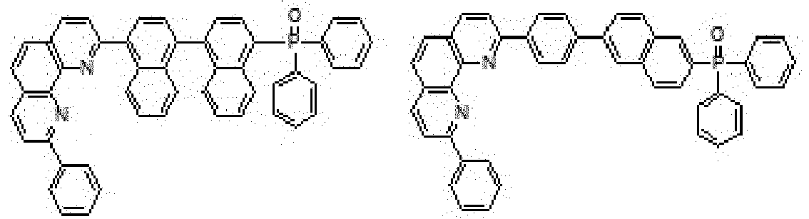


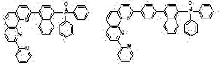


- (7) An organic light emitting diode, comprising:
- first and second electrodes facing each other;
- a first emitting part between the first and second electrodes and including a first emitting material layer and a first electron transporting layer;
- a second emitting part between the first emitting part and the second electrode and including a second emitting material layer and a second electron transporting layer; and
- a first charge generation layer between the first and second emitting parts,
- wherein at least one of the first electron transporting layer, the second electron transporting layer and the first charge generation layer includes the organic compound of aspect (1).
- (8) The organic light emitting diode according to aspect (7), wherein the first charge generation layer includes a P-type charge generation layer and an N-type charge generation layer between the P-type charge generation layer and the first electron transporting layer, and wherein the organic compound is included in the N-type charge generation layer, and the N-type charge generation layer further includes an alkali metal or an alkali earth metal.
- (9) The organic light emitting diode according to aspect (7), further comprising:
- a third emitting part between the second emitting part and the second electrode and including a third emitting material layer and a third electron transporting layer; and
- a second charge generation layer between the second and third emitting parts,
- wherein at least one of the third electron transporting layer and the second charge generation layer includes the organic compound of aspect (1).
- (10) The organic light emitting diode according to aspect (7), wherein the organic compound is selected from:


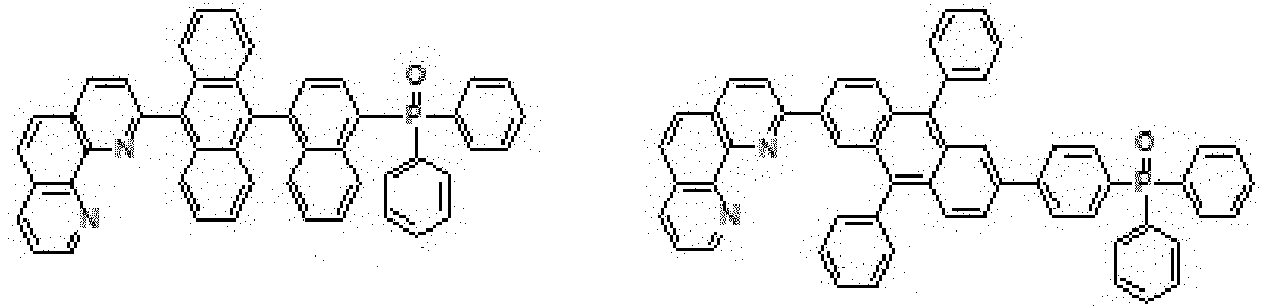


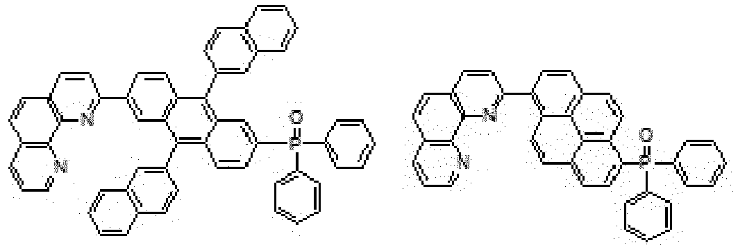
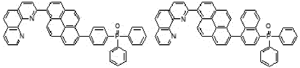


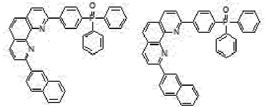


- (11) An organic light emitting display device, comprising:
- a substrate;
- an organic light emitting diode of aspect (4): and
- a thin film transistor between the substrate and the organic light emitting diode and connected to the organic light emitting diode.
- (12) The organic light emitting display device according to aspect (11), wherein the electron transporting layer further includes an alkali metal or an alkali earth metal.
- (13) The organic light emitting display device according to aspect (11), wherein the organic compound is selected from:
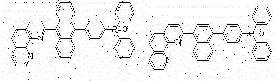


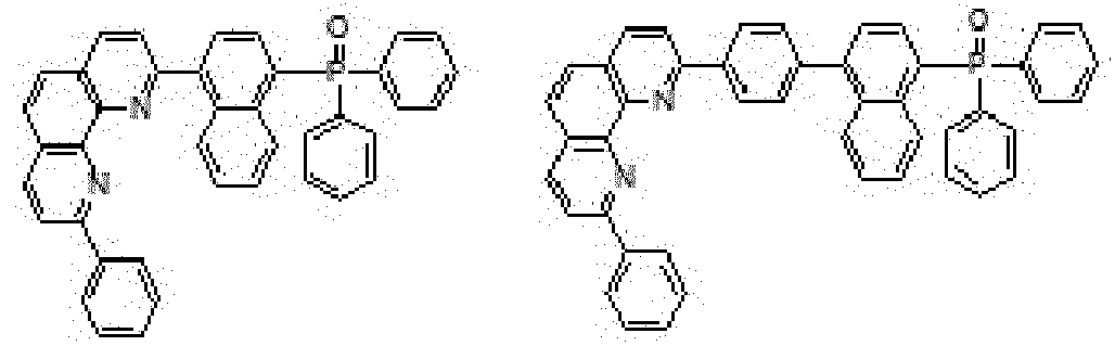


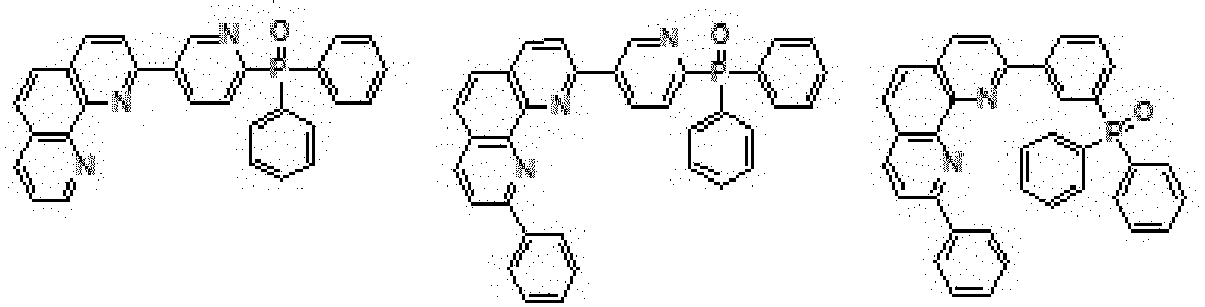
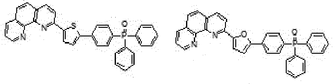


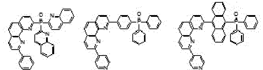

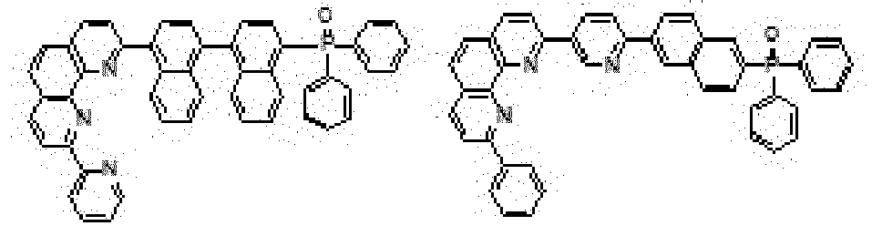


- (14) An organic light emitting display device, comprising:
- a substrate;
- an organic light emitting diode of aspect (7): and
- a thin film transistor between the substrate and the organic light emitting diode and connected to the organic light emitting diode.
- (15) The organic light emitting display device according to aspect (14), wherein the first charge generation layer includes a P-type charge generation layer and an N-type charge generation layer between the P-type charge generation layer and the first electron transporting layer, and wherein the organic compound is included in the N-type charge generation layer, and the N-type charge generation layer further includes an alkali metal or an alkali earth metal.
- (16) The organic light emitting display device according to aspect (14), further comprising:
- a third emitting part between the second emitting part and the second electrode and including a third emitting material layer and a third electron transporting layer; and
- a second charge generation layer between the second and third emitting parts,
- wherein at least one of the third electron transporting layer and the second charge generation layer includes the organic compound of aspect (1).
- (17) The organic light emitting display device according to aspect (14), further comprising a color filter between the substrate and the organic light emitting diode or over the second electrode.
- (18) The organic light emitting display device according to aspect (14), wherein the organic compound is selected from:

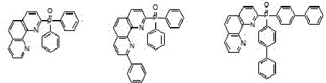


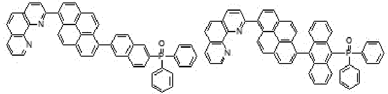


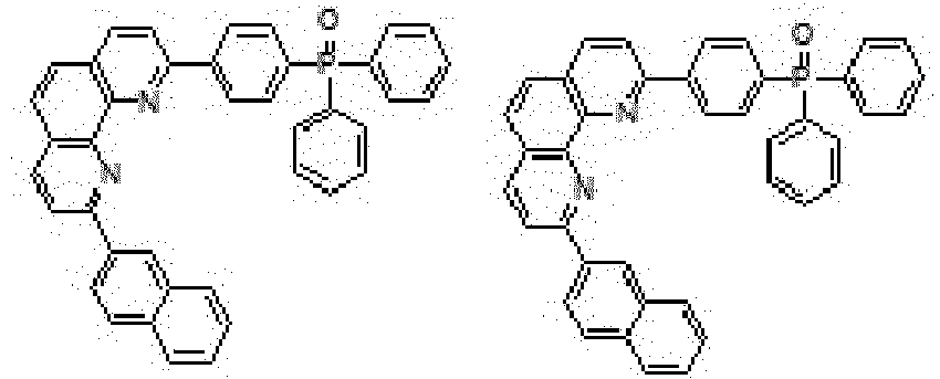


Claims (13)
- An organic compound, represented by following Formula:

wherein a is 2 or 3, b is 1 or 2, c is 2 or 3, and the summation of a, band c is 7,
wherein Ar1 is selected from the group consisting of substituted or non-substituted C1-C20 alkylene, substituted or non-substituted C5-C30 cycloalkylene, substituted or non-substituted C4-C30 heterocycloakylene, substituted or non-substituted C5-C30 arylene and substituted or non-substituted C4-C30 heteroarylene, and each of Ar2 and Ar3 is independently selected from the group consisting of hydrogen, deuterium, tritium, halogen, nitrile, substituted or non-substituted C5-C30 aryl, substituted or non-substituted C4-C30 heteroaryl, substituted or non-substituted C5-C30 oxyaryl and substituted or non-substituted C4-C30 hetero-oxyaryl, and
wherein n is 0, 1 or 2. - The organic compound according to claim 1, wherein Ar1 is selected from substituted or non-substituted C5-C30 arylene and substituted or non-substituted C4-C30 heteroarylene, and each of R1 to R3 is independently selected from substituted or non-substituted C5-C30 aryl or substituted or non-substituted C4-C30 heteroaryl.
- The organic compound according to claim 1, wherein "a" is 3, "b" is 2, "c" is 2, R2 and R3 are hydrogen, at R1 is independently selected from hydrogen, substituted or non-substituted phenyl, substituted or non-substituted pyridyl, substituted or non-substituted naphthyl, wherein the groups R1 are all identical or two are identical and one is different from the other two, "n" is 1 or 2, Ar1 is selected from the group consisting of phenylene, biphenylene, terphenylene, naphthylene, anthracenylene, phenanthrenylene, triphenylene, pyrenylene, fluorenylene, pyridinylene, pyrimidinylene, pyridazinylene, pyrazinylene, benzothiophenylene, dibenzothiophenylene, benzofuranylene and dibenzofuranylene, which may be substituted by C1-C20 alkyl, cyano, C5-C30 aryl or C4-C30 heteroaryl, each of Ar2 and Ar3 is independently selected from substituted or non-substituted phenyl, biphenyl, anthracenyl, pyridyl, pyrimidyl, pyrazinyl, pyridazinyl or carbazolyl.
- The organic compound according to claim 1, wherein the organic compound is selected from:

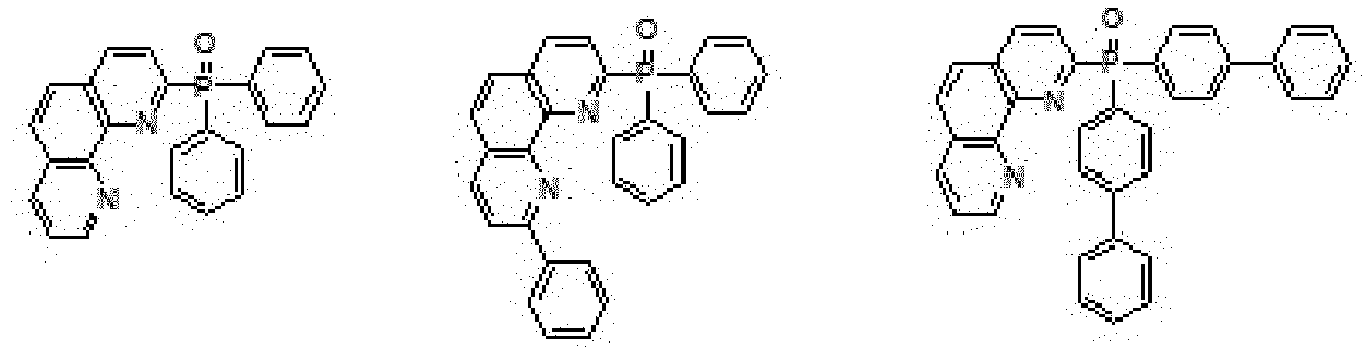


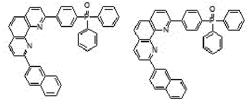
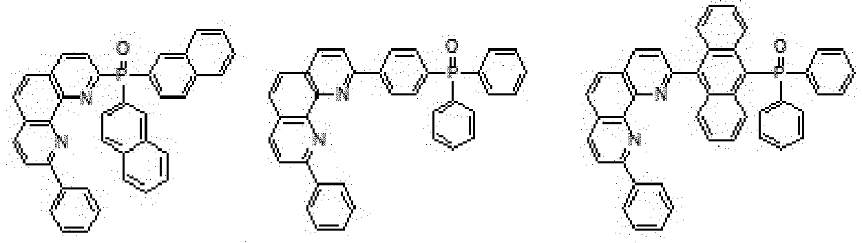


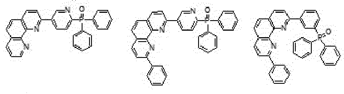

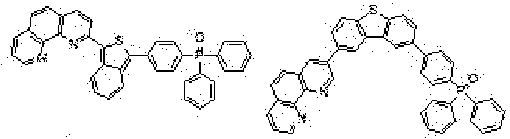


- An organic light emitting diode comprising
an organic compound according to one of claims 1 to 4. - The organic light emitting diode according to claim 5, further comprising first and second electrodes facing each other;
an emitting material layer between the first and second electrodes; and
an electron transporting layer between the emitting material layer and the second electrode. - The organic light emitting diode according to claim 6, wherein the electron transporting layer further includes an alkali metal or an alkali earth metal.
- The organic light emitting diode according to claim 5, further comprising:first and second electrodes facing each other;a first emitting part between the first and second electrodes and including a first emitting material layer and a first electron transporting layer;a second emitting part between the first emitting part and the second electrode and including a second emitting material layer and a second electron transporting layer; anda first charge generation layer between the first and second emitting parts,wherein the organic compound according to one of claims 1 to 4 is included in at least one of the first electron transporting layer, the second electron transporting layer and the first charge generation layer.
- The organic light emitting diode according to claim 8, wherein the first charge generation layer includes a P-type charge generation layer and an N-type charge generation layer between the P-type charge generation layer and the first electron transporting layer, and wherein the organic compound is included in the N-type charge generation layer, and the N-type charge generation layer further includes an alkali metal or an alkali earth metal.
- The organic light emitting diode according to claim 8, further comprising:a third emitting part between the second emitting part and the second electrode and including a third emitting material layer and a third electron transporting layer; anda second charge generation layer between the second and third emitting parts,wherein at least one of the third electron transporting layer and the second charge generation layer includes the organic compound according to one of claims 1 to 4.
- An organic light emitting display device, comprising:a substrate;an organic light emitting diode according to one of claims 5 to 10; anda thin film transistor between the substrate and the organic light emitting diode and connected to the organic light emitting diode.
- The organic light emitting display device according to claim 11, further comprising a color filter between the substrate and the organic light emitting diode or over the second electrode.
- Use of an organic compound according to one of claims 1 to 4 in an organic light emitting diode according to one of claims 5 to 10 or an organic light emitting display device according to one of claims 11 or 12.
Applications Claiming Priority (1)
| Application Number | Priority Date | Filing Date | Title |
|---|---|---|---|
| KR1020160143283A KR101891168B1 (en) | 2016-10-31 | 2016-10-31 | Organic compound and organic light emitting diode and organic light emittid display device having the compound |
Publications (2)
| Publication Number | Publication Date |
|---|---|
| EP3316334A1 true EP3316334A1 (en) | 2018-05-02 |
| EP3316334B1 EP3316334B1 (en) | 2020-08-26 |
Family
ID=60186119
Family Applications (1)
| Application Number | Title | Priority Date | Filing Date |
|---|---|---|---|
| EP17198447.9A Active EP3316334B1 (en) | 2016-10-31 | 2017-10-26 | Organic light emitting diode and organic light emitting display device |
Country Status (4)
| Country | Link |
|---|---|
| US (1) | US11155543B2 (en) |
| EP (1) | EP3316334B1 (en) |
| KR (1) | KR101891168B1 (en) |
| CN (1) | CN108017672B (en) |
Cited By (1)
| Publication number | Priority date | Publication date | Assignee | Title |
|---|---|---|---|---|
| EP3667755A1 (en) * | 2018-12-14 | 2020-06-17 | Novaled GmbH | Organic light emitting device, a method for manufacturing the same and a composition for use therein |
Families Citing this family (12)
| Publication number | Priority date | Publication date | Assignee | Title |
|---|---|---|---|---|
| KR102309894B1 (en) * | 2017-03-14 | 2021-10-07 | 삼성디스플레이 주식회사 | Light emitting diode and display device including the same |
| KR102027512B1 (en) * | 2017-12-22 | 2019-10-01 | 엘지디스플레이 주식회사 | Organic light emitting diode and organic light emittind display device having the same |
| GB201812402D0 (en) * | 2018-07-30 | 2018-09-12 | Savvy Science Ltd | Perovskite light emitting device with multiple emissive layers |
| CN109585665A (en) * | 2018-11-30 | 2019-04-05 | 云谷(固安)科技有限公司 | A kind of light-emitting component and display device |
| CN111377965A (en) * | 2018-12-28 | 2020-07-07 | 上海和辉光电有限公司 | Organic light-emitting material and OLED device |
| KR102349278B1 (en) | 2019-09-03 | 2022-01-11 | 삼성디스플레이 주식회사 | Organic light emitting device |
| US12268089B2 (en) * | 2020-05-29 | 2025-04-01 | Lg Display Co., Ltd. | Organic light emitting device |
| US12324349B2 (en) * | 2020-06-08 | 2025-06-03 | Samsung Display Co., Ltd. | Organometallic compound and organic light-emitting device including the same |
| EP3993077A1 (en) | 2020-10-29 | 2022-05-04 | Imec VZW | Contaminated interface mitigation in a semiconductor device |
| KR20220072897A (en) * | 2020-11-24 | 2022-06-03 | 삼성디스플레이 주식회사 | light emitting device and electronic device including the light emitting device |
| KR20220126327A (en) * | 2021-03-08 | 2022-09-16 | 삼성디스플레이 주식회사 | Organometallic compound, light-emitting device including the same, and electronic device including the light-emitting device |
| CN119219700B (en) * | 2024-11-28 | 2025-05-23 | 石家庄诚志永华显示材料有限公司 | Compound with phenanthroline structure, organic electroluminescent device comprising same and display device |
Citations (9)
| Publication number | Priority date | Publication date | Assignee | Title |
|---|---|---|---|---|
| JP2004204140A (en) * | 2002-12-26 | 2004-07-22 | Toray Ind Inc | Light emitting device material and light emitting device using the same |
| JP2006073581A (en) * | 2004-08-31 | 2006-03-16 | Toray Ind Inc | Light emitting device material and light emitting device |
| JP2008071993A (en) * | 2006-09-15 | 2008-03-27 | Toray Ind Inc | Light emitting element |
| US20160005980A1 (en) * | 2014-07-03 | 2016-01-07 | Samsung Display Co., Ltd. | Organic light-emitting device |
| US20160005979A1 (en) * | 2014-07-02 | 2016-01-07 | Samsung Display Co., Ltd. | Organic light-emitting device |
| US20160013427A1 (en) * | 2014-07-10 | 2016-01-14 | Samsung Display Co., Ltd. | Organic light-emitting device |
| US20160020405A1 (en) * | 2014-07-10 | 2016-01-21 | Samsung Display Co., Ltd. | Organic light emitting element and organic light emitting display device including the same |
| EP2983227A1 (en) * | 2014-08-01 | 2016-02-10 | LG Display Co., Ltd. | Organic light emitting display device |
| KR20160053048A (en) * | 2014-10-30 | 2016-05-13 | 삼성디스플레이 주식회사 | Phosphine oxide-based compound and organic light emitting device comprising the same |
Family Cites Families (7)
| Publication number | Priority date | Publication date | Assignee | Title |
|---|---|---|---|---|
| KR100647660B1 (en) * | 2004-11-19 | 2006-11-23 | 삼성에스디아이 주식회사 | Thin film transistor and flat panel display device using same |
| KR100879477B1 (en) * | 2007-10-11 | 2009-01-20 | 삼성모바일디스플레이주식회사 | Organic light emitting device |
| CN103374040B (en) * | 2013-07-02 | 2016-01-06 | 华南理工大学 | One class contains the alcohol dissolubility cathode buffer layer molecule-type material of triaryl phosphorus oxygen and nitrogen heterocyclic functional group and synthetic method thereof and application |
| KR102315538B1 (en) * | 2014-11-04 | 2021-10-25 | 코웨이 주식회사 | Ice maker, water treatment apparatus having ice maker and method for making ice |
| KR102294413B1 (en) * | 2014-11-18 | 2021-08-27 | 삼성디스플레이 주식회사 | Organice light emitting diode display |
| TWI613210B (en) * | 2015-03-05 | 2018-02-01 | Lg 化學股份有限公司 | Heterocyclic compound and organic light-emitting element containing the same |
| CN105693773B (en) * | 2016-02-29 | 2018-05-15 | 华南理工大学 | A kind of organic molecule electron transport material with high triplet energy level and preparation method thereof, application |
-
2016
- 2016-10-31 KR KR1020160143283A patent/KR101891168B1/en active Active
-
2017
- 2017-10-12 CN CN201710948852.7A patent/CN108017672B/en active Active
- 2017-10-26 EP EP17198447.9A patent/EP3316334B1/en active Active
- 2017-10-31 US US15/799,421 patent/US11155543B2/en active Active
Patent Citations (9)
| Publication number | Priority date | Publication date | Assignee | Title |
|---|---|---|---|---|
| JP2004204140A (en) * | 2002-12-26 | 2004-07-22 | Toray Ind Inc | Light emitting device material and light emitting device using the same |
| JP2006073581A (en) * | 2004-08-31 | 2006-03-16 | Toray Ind Inc | Light emitting device material and light emitting device |
| JP2008071993A (en) * | 2006-09-15 | 2008-03-27 | Toray Ind Inc | Light emitting element |
| US20160005979A1 (en) * | 2014-07-02 | 2016-01-07 | Samsung Display Co., Ltd. | Organic light-emitting device |
| US20160005980A1 (en) * | 2014-07-03 | 2016-01-07 | Samsung Display Co., Ltd. | Organic light-emitting device |
| US20160013427A1 (en) * | 2014-07-10 | 2016-01-14 | Samsung Display Co., Ltd. | Organic light-emitting device |
| US20160020405A1 (en) * | 2014-07-10 | 2016-01-21 | Samsung Display Co., Ltd. | Organic light emitting element and organic light emitting display device including the same |
| EP2983227A1 (en) * | 2014-08-01 | 2016-02-10 | LG Display Co., Ltd. | Organic light emitting display device |
| KR20160053048A (en) * | 2014-10-30 | 2016-05-13 | 삼성디스플레이 주식회사 | Phosphine oxide-based compound and organic light emitting device comprising the same |
Cited By (2)
| Publication number | Priority date | Publication date | Assignee | Title |
|---|---|---|---|---|
| EP3667755A1 (en) * | 2018-12-14 | 2020-06-17 | Novaled GmbH | Organic light emitting device, a method for manufacturing the same and a composition for use therein |
| WO2020120791A1 (en) * | 2018-12-14 | 2020-06-18 | Novaled Gmbh | Organic light emitting device, a method for manufacturing the same and a composition for use therein |
Also Published As
| Publication number | Publication date |
|---|---|
| US20180118742A1 (en) | 2018-05-03 |
| KR20180047311A (en) | 2018-05-10 |
| KR101891168B1 (en) | 2018-08-23 |
| CN108017672B (en) | 2021-04-09 |
| EP3316334B1 (en) | 2020-08-26 |
| CN108017672A (en) | 2018-05-11 |
| US11155543B2 (en) | 2021-10-26 |
Similar Documents
| Publication | Publication Date | Title |
|---|---|---|
| US11856846B2 (en) | Organic compound, and organic light emitting diode and organic light emitting display device including the same | |
| EP3316334B1 (en) | Organic light emitting diode and organic light emitting display device | |
| KR102157756B1 (en) | Organic compounds and organic light emitting diode and organic light emittind display device having the same | |
| US10615347B2 (en) | Organic compound, and organic light emitting diode and organic light emitting display device including the same | |
| EP4038667B1 (en) | Organic light emitting diode and organic light emitting device having the same | |
| US10700290B2 (en) | Organic compound, and organic light-emitting diode and organic light-emitting diode display device including the same | |
| KR102784370B1 (en) | Organic compound and light emitting diode and organic light emitting diode display device using the same | |
| KR102649051B1 (en) | Organic compound and light emitting diode and organic light emitting diode display device using the same | |
| KR102689354B1 (en) | Organic compounds, organic light emitting diode and organic light emittid device having the compounds | |
| KR102642605B1 (en) | Organic compound, organic light emitting diode and organic light emiting device having the compound | |
| KR102630959B1 (en) | Organic compound and light emitting diode and organic light emitting diode display device using the same | |
| KR20190063923A (en) | Organic compounds, organic light emitting diode and orgnic light emitting device having the compounds | |
| KR20190027540A (en) | Organic compounds, organic light emitting diode and orgnic light emitting device having the compounds | |
| KR102515819B1 (en) | Organic compounds, organic light emitting diode and organic light emittid device having the compounds | |
| KR101957669B1 (en) | Organic compound and organic light emitting diode and organic light emittid display device having the compound | |
| KR20190027537A (en) | Organic compounds, organic light emitting diode and orgnic light emitting device having the compounds | |
| KR102451310B1 (en) | Organic compounds, organic light emitting diode and organic light emittid device having the compounds | |
| KR102686826B1 (en) | Organic compound and light emitting diode and organic light emitting diode display device using the same | |
| KR20190061748A (en) | Organic compounds, organic light emitting diode and organic light emittid device having the compounds | |
| KR102577042B1 (en) | Organic compounds, organic light emitting diode and organic light emittid device having the compounds | |
| CN118265327A (en) | Organic light emitting diode and organic light emitting device including the same |
Legal Events
| Date | Code | Title | Description |
|---|---|---|---|
| PUAI | Public reference made under article 153(3) epc to a published international application that has entered the european phase |
Free format text: ORIGINAL CODE: 0009012 |
|
| STAA | Information on the status of an ep patent application or granted ep patent |
Free format text: STATUS: REQUEST FOR EXAMINATION WAS MADE |
|
| 17P | Request for examination filed |
Effective date: 20171026 |
|
| AK | Designated contracting states |
Kind code of ref document: A1 Designated state(s): AL AT BE BG CH CY CZ DE DK EE ES FI FR GB GR HR HU IE IS IT LI LT LU LV MC MK MT NL NO PL PT RO RS SE SI SK SM TR |
|
| AX | Request for extension of the european patent |
Extension state: BA ME |
|
| RBV | Designated contracting states (corrected) |
Designated state(s): AL AT BE BG CH CY CZ DE DK EE ES FI FR GB GR HR HU IE IS IT LI LT LU LV MC MK MT NL NO PL PT RO RS SE SI SK SM TR |
|
| GRAP | Despatch of communication of intention to grant a patent |
Free format text: ORIGINAL CODE: EPIDOSNIGR1 |
|
| STAA | Information on the status of an ep patent application or granted ep patent |
Free format text: STATUS: GRANT OF PATENT IS INTENDED |
|
| RIC1 | Information provided on ipc code assigned before grant |
Ipc: H01L 51/54 20060101AFI20200318BHEP |
|
| INTG | Intention to grant announced |
Effective date: 20200403 |
|
| GRAS | Grant fee paid |
Free format text: ORIGINAL CODE: EPIDOSNIGR3 |
|
| GRAA | (expected) grant |
Free format text: ORIGINAL CODE: 0009210 |
|
| STAA | Information on the status of an ep patent application or granted ep patent |
Free format text: STATUS: THE PATENT HAS BEEN GRANTED |
|
| AK | Designated contracting states |
Kind code of ref document: B1 Designated state(s): AL AT BE BG CH CY CZ DE DK EE ES FI FR GB GR HR HU IE IS IT LI LT LU LV MC MK MT NL NO PL PT RO RS SE SI SK SM TR |
|
| REG | Reference to a national code |
Ref country code: GB Ref legal event code: FG4D |
|
| REG | Reference to a national code |
Ref country code: CH Ref legal event code: EP |
|
| REG | Reference to a national code |
Ref country code: AT Ref legal event code: REF Ref document number: 1307248 Country of ref document: AT Kind code of ref document: T Effective date: 20200915 |
|
| REG | Reference to a national code |
Ref country code: IE Ref legal event code: FG4D |
|
| REG | Reference to a national code |
Ref country code: DE Ref legal event code: R096 Ref document number: 602017022280 Country of ref document: DE |
|
| REG | Reference to a national code |
Ref country code: LT Ref legal event code: MG4D |
|
| PG25 | Lapsed in a contracting state [announced via postgrant information from national office to epo] |
Ref country code: PT Free format text: LAPSE BECAUSE OF FAILURE TO SUBMIT A TRANSLATION OF THE DESCRIPTION OR TO PAY THE FEE WITHIN THE PRESCRIBED TIME-LIMIT Effective date: 20201228 Ref country code: GR Free format text: LAPSE BECAUSE OF FAILURE TO SUBMIT A TRANSLATION OF THE DESCRIPTION OR TO PAY THE FEE WITHIN THE PRESCRIBED TIME-LIMIT Effective date: 20201127 Ref country code: BG Free format text: LAPSE BECAUSE OF FAILURE TO SUBMIT A TRANSLATION OF THE DESCRIPTION OR TO PAY THE FEE WITHIN THE PRESCRIBED TIME-LIMIT Effective date: 20201126 Ref country code: NO Free format text: LAPSE BECAUSE OF FAILURE TO SUBMIT A TRANSLATION OF THE DESCRIPTION OR TO PAY THE FEE WITHIN THE PRESCRIBED TIME-LIMIT Effective date: 20201126 Ref country code: FI Free format text: LAPSE BECAUSE OF FAILURE TO SUBMIT A TRANSLATION OF THE DESCRIPTION OR TO PAY THE FEE WITHIN THE PRESCRIBED TIME-LIMIT Effective date: 20200826 Ref country code: LT Free format text: LAPSE BECAUSE OF FAILURE TO SUBMIT A TRANSLATION OF THE DESCRIPTION OR TO PAY THE FEE WITHIN THE PRESCRIBED TIME-LIMIT Effective date: 20200826 Ref country code: SE Free format text: LAPSE BECAUSE OF FAILURE TO SUBMIT A TRANSLATION OF THE DESCRIPTION OR TO PAY THE FEE WITHIN THE PRESCRIBED TIME-LIMIT Effective date: 20200826 Ref country code: HR Free format text: LAPSE BECAUSE OF FAILURE TO SUBMIT A TRANSLATION OF THE DESCRIPTION OR TO PAY THE FEE WITHIN THE PRESCRIBED TIME-LIMIT Effective date: 20200826 |
|
| REG | Reference to a national code |
Ref country code: NL Ref legal event code: MP Effective date: 20200826 |
|
| REG | Reference to a national code |
Ref country code: AT Ref legal event code: MK05 Ref document number: 1307248 Country of ref document: AT Kind code of ref document: T Effective date: 20200826 |
|
| PG25 | Lapsed in a contracting state [announced via postgrant information from national office to epo] |
Ref country code: LV Free format text: LAPSE BECAUSE OF FAILURE TO SUBMIT A TRANSLATION OF THE DESCRIPTION OR TO PAY THE FEE WITHIN THE PRESCRIBED TIME-LIMIT Effective date: 20200826 Ref country code: PL Free format text: LAPSE BECAUSE OF FAILURE TO SUBMIT A TRANSLATION OF THE DESCRIPTION OR TO PAY THE FEE WITHIN THE PRESCRIBED TIME-LIMIT Effective date: 20200826 Ref country code: RS Free format text: LAPSE BECAUSE OF FAILURE TO SUBMIT A TRANSLATION OF THE DESCRIPTION OR TO PAY THE FEE WITHIN THE PRESCRIBED TIME-LIMIT Effective date: 20200826 Ref country code: NL Free format text: LAPSE BECAUSE OF FAILURE TO SUBMIT A TRANSLATION OF THE DESCRIPTION OR TO PAY THE FEE WITHIN THE PRESCRIBED TIME-LIMIT Effective date: 20200826 Ref country code: IS Free format text: LAPSE BECAUSE OF FAILURE TO SUBMIT A TRANSLATION OF THE DESCRIPTION OR TO PAY THE FEE WITHIN THE PRESCRIBED TIME-LIMIT Effective date: 20201226 |
|
| PG25 | Lapsed in a contracting state [announced via postgrant information from national office to epo] |
Ref country code: DK Free format text: LAPSE BECAUSE OF FAILURE TO SUBMIT A TRANSLATION OF THE DESCRIPTION OR TO PAY THE FEE WITHIN THE PRESCRIBED TIME-LIMIT Effective date: 20200826 Ref country code: CZ Free format text: LAPSE BECAUSE OF FAILURE TO SUBMIT A TRANSLATION OF THE DESCRIPTION OR TO PAY THE FEE WITHIN THE PRESCRIBED TIME-LIMIT Effective date: 20200826 Ref country code: RO Free format text: LAPSE BECAUSE OF FAILURE TO SUBMIT A TRANSLATION OF THE DESCRIPTION OR TO PAY THE FEE WITHIN THE PRESCRIBED TIME-LIMIT Effective date: 20200826 Ref country code: EE Free format text: LAPSE BECAUSE OF FAILURE TO SUBMIT A TRANSLATION OF THE DESCRIPTION OR TO PAY THE FEE WITHIN THE PRESCRIBED TIME-LIMIT Effective date: 20200826 Ref country code: SM Free format text: LAPSE BECAUSE OF FAILURE TO SUBMIT A TRANSLATION OF THE DESCRIPTION OR TO PAY THE FEE WITHIN THE PRESCRIBED TIME-LIMIT Effective date: 20200826 |
|
| REG | Reference to a national code |
Ref country code: DE Ref legal event code: R097 Ref document number: 602017022280 Country of ref document: DE |
|
| PG25 | Lapsed in a contracting state [announced via postgrant information from national office to epo] |
Ref country code: ES Free format text: LAPSE BECAUSE OF FAILURE TO SUBMIT A TRANSLATION OF THE DESCRIPTION OR TO PAY THE FEE WITHIN THE PRESCRIBED TIME-LIMIT Effective date: 20200826 Ref country code: AT Free format text: LAPSE BECAUSE OF FAILURE TO SUBMIT A TRANSLATION OF THE DESCRIPTION OR TO PAY THE FEE WITHIN THE PRESCRIBED TIME-LIMIT Effective date: 20200826 Ref country code: AL Free format text: LAPSE BECAUSE OF FAILURE TO SUBMIT A TRANSLATION OF THE DESCRIPTION OR TO PAY THE FEE WITHIN THE PRESCRIBED TIME-LIMIT Effective date: 20200826 |
|
| REG | Reference to a national code |
Ref country code: CH Ref legal event code: PL |
|
| PG25 | Lapsed in a contracting state [announced via postgrant information from national office to epo] |
Ref country code: LU Free format text: LAPSE BECAUSE OF NON-PAYMENT OF DUE FEES Effective date: 20201026 Ref country code: MC Free format text: LAPSE BECAUSE OF FAILURE TO SUBMIT A TRANSLATION OF THE DESCRIPTION OR TO PAY THE FEE WITHIN THE PRESCRIBED TIME-LIMIT Effective date: 20200826 Ref country code: SK Free format text: LAPSE BECAUSE OF FAILURE TO SUBMIT A TRANSLATION OF THE DESCRIPTION OR TO PAY THE FEE WITHIN THE PRESCRIBED TIME-LIMIT Effective date: 20200826 |
|
| PLBE | No opposition filed within time limit |
Free format text: ORIGINAL CODE: 0009261 |
|
| STAA | Information on the status of an ep patent application or granted ep patent |
Free format text: STATUS: NO OPPOSITION FILED WITHIN TIME LIMIT |
|
| REG | Reference to a national code |
Ref country code: BE Ref legal event code: MM Effective date: 20201031 |
|
| PG25 | Lapsed in a contracting state [announced via postgrant information from national office to epo] |
Ref country code: IT Free format text: LAPSE BECAUSE OF FAILURE TO SUBMIT A TRANSLATION OF THE DESCRIPTION OR TO PAY THE FEE WITHIN THE PRESCRIBED TIME-LIMIT Effective date: 20200826 |
|
| 26N | No opposition filed |
Effective date: 20210527 |
|
| PG25 | Lapsed in a contracting state [announced via postgrant information from national office to epo] |
Ref country code: LI Free format text: LAPSE BECAUSE OF NON-PAYMENT OF DUE FEES Effective date: 20201031 Ref country code: SI Free format text: LAPSE BECAUSE OF FAILURE TO SUBMIT A TRANSLATION OF THE DESCRIPTION OR TO PAY THE FEE WITHIN THE PRESCRIBED TIME-LIMIT Effective date: 20200826 Ref country code: BE Free format text: LAPSE BECAUSE OF NON-PAYMENT OF DUE FEES Effective date: 20201031 Ref country code: CH Free format text: LAPSE BECAUSE OF NON-PAYMENT OF DUE FEES Effective date: 20201031 |
|
| PG25 | Lapsed in a contracting state [announced via postgrant information from national office to epo] |
Ref country code: IE Free format text: LAPSE BECAUSE OF NON-PAYMENT OF DUE FEES Effective date: 20201026 |
|
| PG25 | Lapsed in a contracting state [announced via postgrant information from national office to epo] |
Ref country code: TR Free format text: LAPSE BECAUSE OF FAILURE TO SUBMIT A TRANSLATION OF THE DESCRIPTION OR TO PAY THE FEE WITHIN THE PRESCRIBED TIME-LIMIT Effective date: 20200826 Ref country code: MT Free format text: LAPSE BECAUSE OF FAILURE TO SUBMIT A TRANSLATION OF THE DESCRIPTION OR TO PAY THE FEE WITHIN THE PRESCRIBED TIME-LIMIT Effective date: 20200826 Ref country code: CY Free format text: LAPSE BECAUSE OF FAILURE TO SUBMIT A TRANSLATION OF THE DESCRIPTION OR TO PAY THE FEE WITHIN THE PRESCRIBED TIME-LIMIT Effective date: 20200826 |
|
| PG25 | Lapsed in a contracting state [announced via postgrant information from national office to epo] |
Ref country code: MK Free format text: LAPSE BECAUSE OF FAILURE TO SUBMIT A TRANSLATION OF THE DESCRIPTION OR TO PAY THE FEE WITHIN THE PRESCRIBED TIME-LIMIT Effective date: 20200826 |
|
| REG | Reference to a national code |
Ref country code: DE Ref legal event code: R079 Ref document number: 602017022280 Country of ref document: DE Free format text: PREVIOUS MAIN CLASS: H01L0051540000 Ipc: H10K0085000000 |
|
| PGFP | Annual fee paid to national office [announced via postgrant information from national office to epo] |
Ref country code: GB Payment date: 20250820 Year of fee payment: 9 |
|
| PGFP | Annual fee paid to national office [announced via postgrant information from national office to epo] |
Ref country code: FR Payment date: 20250821 Year of fee payment: 9 |
|
| PGFP | Annual fee paid to national office [announced via postgrant information from national office to epo] |
Ref country code: DE Payment date: 20250820 Year of fee payment: 9 |