EP3316097A1 - In-cell touch organic light-emitting display device - Google Patents
In-cell touch organic light-emitting display device Download PDFInfo
- Publication number
- EP3316097A1 EP3316097A1 EP17199482.5A EP17199482A EP3316097A1 EP 3316097 A1 EP3316097 A1 EP 3316097A1 EP 17199482 A EP17199482 A EP 17199482A EP 3316097 A1 EP3316097 A1 EP 3316097A1
- Authority
- EP
- European Patent Office
- Prior art keywords
- electrodes
- portions
- organic light
- display device
- brightness
- Prior art date
- Legal status (The legal status is an assumption and is not a legal conclusion. Google has not performed a legal analysis and makes no representation as to the accuracy of the status listed.)
- Granted
Links
Images




Classifications
-
- G—PHYSICS
- G06—COMPUTING OR CALCULATING; COUNTING
- G06F—ELECTRIC DIGITAL DATA PROCESSING
- G06F3/00—Input arrangements for transferring data to be processed into a form capable of being handled by the computer; Output arrangements for transferring data from processing unit to output unit, e.g. interface arrangements
- G06F3/01—Input arrangements or combined input and output arrangements for interaction between user and computer
- G06F3/03—Arrangements for converting the position or the displacement of a member into a coded form
- G06F3/041—Digitisers, e.g. for touch screens or touch pads, characterised by the transducing means
- G06F3/0412—Digitisers structurally integrated in a display
-
- G—PHYSICS
- G06—COMPUTING OR CALCULATING; COUNTING
- G06F—ELECTRIC DIGITAL DATA PROCESSING
- G06F3/00—Input arrangements for transferring data to be processed into a form capable of being handled by the computer; Output arrangements for transferring data from processing unit to output unit, e.g. interface arrangements
- G06F3/01—Input arrangements or combined input and output arrangements for interaction between user and computer
- G06F3/03—Arrangements for converting the position or the displacement of a member into a coded form
- G06F3/041—Digitisers, e.g. for touch screens or touch pads, characterised by the transducing means
- G06F3/0416—Control or interface arrangements specially adapted for digitisers
-
- G—PHYSICS
- G06—COMPUTING OR CALCULATING; COUNTING
- G06F—ELECTRIC DIGITAL DATA PROCESSING
- G06F3/00—Input arrangements for transferring data to be processed into a form capable of being handled by the computer; Output arrangements for transferring data from processing unit to output unit, e.g. interface arrangements
- G06F3/01—Input arrangements or combined input and output arrangements for interaction between user and computer
- G06F3/03—Arrangements for converting the position or the displacement of a member into a coded form
- G06F3/041—Digitisers, e.g. for touch screens or touch pads, characterised by the transducing means
- G06F3/044—Digitisers, e.g. for touch screens or touch pads, characterised by the transducing means by capacitive means
-
- G—PHYSICS
- G06—COMPUTING OR CALCULATING; COUNTING
- G06F—ELECTRIC DIGITAL DATA PROCESSING
- G06F3/00—Input arrangements for transferring data to be processed into a form capable of being handled by the computer; Output arrangements for transferring data from processing unit to output unit, e.g. interface arrangements
- G06F3/01—Input arrangements or combined input and output arrangements for interaction between user and computer
- G06F3/03—Arrangements for converting the position or the displacement of a member into a coded form
- G06F3/041—Digitisers, e.g. for touch screens or touch pads, characterised by the transducing means
- G06F3/044—Digitisers, e.g. for touch screens or touch pads, characterised by the transducing means by capacitive means
- G06F3/0443—Digitisers, e.g. for touch screens or touch pads, characterised by the transducing means by capacitive means using a single layer of sensing electrodes
-
- G—PHYSICS
- G06—COMPUTING OR CALCULATING; COUNTING
- G06F—ELECTRIC DIGITAL DATA PROCESSING
- G06F3/00—Input arrangements for transferring data to be processed into a form capable of being handled by the computer; Output arrangements for transferring data from processing unit to output unit, e.g. interface arrangements
- G06F3/01—Input arrangements or combined input and output arrangements for interaction between user and computer
- G06F3/03—Arrangements for converting the position or the displacement of a member into a coded form
- G06F3/041—Digitisers, e.g. for touch screens or touch pads, characterised by the transducing means
- G06F3/044—Digitisers, e.g. for touch screens or touch pads, characterised by the transducing means by capacitive means
- G06F3/0446—Digitisers, e.g. for touch screens or touch pads, characterised by the transducing means by capacitive means using a grid-like structure of electrodes in at least two directions, e.g. using row and column electrodes
-
- H—ELECTRICITY
- H10—SEMICONDUCTOR DEVICES; ELECTRIC SOLID-STATE DEVICES NOT OTHERWISE PROVIDED FOR
- H10K—ORGANIC ELECTRIC SOLID-STATE DEVICES
- H10K50/00—Organic light-emitting devices
- H10K50/80—Constructional details
- H10K50/805—Electrodes
-
- H—ELECTRICITY
- H10—SEMICONDUCTOR DEVICES; ELECTRIC SOLID-STATE DEVICES NOT OTHERWISE PROVIDED FOR
- H10K—ORGANIC ELECTRIC SOLID-STATE DEVICES
- H10K59/00—Integrated devices, or assemblies of multiple devices, comprising at least one organic light-emitting element covered by group H10K50/00
- H10K59/40—OLEDs integrated with touch screens
-
- H—ELECTRICITY
- H10—SEMICONDUCTOR DEVICES; ELECTRIC SOLID-STATE DEVICES NOT OTHERWISE PROVIDED FOR
- H10K—ORGANIC ELECTRIC SOLID-STATE DEVICES
- H10K59/00—Integrated devices, or assemblies of multiple devices, comprising at least one organic light-emitting element covered by group H10K50/00
- H10K59/80—Constructional details
- H10K59/805—Electrodes
-
- G—PHYSICS
- G06—COMPUTING OR CALCULATING; COUNTING
- G06F—ELECTRIC DIGITAL DATA PROCESSING
- G06F2203/00—Indexing scheme relating to G06F3/00 - G06F3/048
- G06F2203/041—Indexing scheme relating to G06F3/041 - G06F3/045
- G06F2203/04102—Flexible digitiser, i.e. constructional details for allowing the whole digitising part of a device to be flexed or rolled like a sheet of paper
-
- G—PHYSICS
- G06—COMPUTING OR CALCULATING; COUNTING
- G06F—ELECTRIC DIGITAL DATA PROCESSING
- G06F2203/00—Indexing scheme relating to G06F3/00 - G06F3/048
- G06F2203/041—Indexing scheme relating to G06F3/041 - G06F3/045
- G06F2203/04112—Electrode mesh in capacitive digitiser: electrode for touch sensing is formed of a mesh of very fine, normally metallic, interconnected lines that are almost invisible to see. This provides a quite large but transparent electrode surface, without need for ITO or similar transparent conductive material
-
- H—ELECTRICITY
- H10—SEMICONDUCTOR DEVICES; ELECTRIC SOLID-STATE DEVICES NOT OTHERWISE PROVIDED FOR
- H10K—ORGANIC ELECTRIC SOLID-STATE DEVICES
- H10K59/00—Integrated devices, or assemblies of multiple devices, comprising at least one organic light-emitting element covered by group H10K50/00
- H10K59/10—OLED displays
- H10K59/12—Active-matrix OLED [AMOLED] displays
- H10K59/131—Interconnections, e.g. wiring lines or terminals
Definitions
- the present disclosure relates to an organic light-emitting display device, and more particularly to an organic light-emitting display device including a metal mesh pattern.
- An image display device which realizes various pieces of information on a screen, is a core technology of the information and communication age, and is being developed in the direction of becoming thinner, lighter, more portable, and having higher performance.
- a flat panel display device that is capable of overcoming the problems of disadvantageous weight and volume of a cathode ray tube (CRT), for example, an organic light-emitting display device, which displays an image by controlling the intensity of luminescence of an organic emission layer, is attracting attention.
- CTR cathode ray tube
- the organic light-emitting display device described above uses a self-illuminating organic light-emitting element, and therefore does not require a separate light source and enables realization of a super-thin-type display.
- a touch-panel-integrated display device having an in-cell touch structure which uses an organic light-emitting element and includes a touch electrode array inside a light-emitting cell, has been actively conducted.
- a touch panel includes a first touch electrode, which is arranged in a first direction, and a second touch electrode, which is arranged in a second direction so as to intersect the first touch electrode.
- the first touch electrode and the second touch electrode are electrically isolated from each other. In this state, when an object charged with static electricity is brought into contact with the touch panel, the touch panel detects a touch input by sensing the change of mutual capacitance between the first touch electrode and the second touch electrode.
- the metal mesh electrode has higher reflectivity than a transparent conductive material, it has a high possibility of being visible to the outside and deteriorates the overall brightness of the organic light-emitting display device.
- the present disclosure is directed to an organic light-emitting display device that substantially addresses one or more problems due to limitations and disadvantages of the related art.
- the present disclosure seeks to provide an organic light-emitting display device, which has improved color viewing angle characteristics while including a mesh pattern.
- an organic light-emitting display device includes an organic light-emitting array including a plurality of pixel openings, and a touch electrode array bonded to the organic light-emitting array.
- the touch electrode array includes a plurality of first mesh electrodes arranged in a first direction and having a structure having multiple lattice portions, and a plurality of second mesh electrodes arranged in a second direction and having a structure having multiple lattice portions.
- Each of the first mesh electrodes and the second mesh electrodes may include a plurality of overlapping portions that overlap the pixel openings and a plurality of non-overlapping portions positioned between the pixel openings.
- At least some of the overlapping portions may include brightness-increasing portions, which are formed of a material different from that of the non-overlapping portions.
- the lattice portions may be positioned on the pixel openings so as to overlap the pixel openings.
- the brightness-increasing portions may include at least one of two line electrodes that form each lattice portion.
- the brightness-increasing portions may be formed of a transparent conductive material.
- each constituent element is illustrated merely for convenience of description, and the present disclosure is not necessarily limited to the illustrated size and thickness of each constituent element.
- FIG. 1 is a plan view for explaining an organic light-emitting display device according to an embodiment.
- An organic light-emitting display device includes a plurality of first mesh electrodes 101, which are arranged on a substrate 1000 in a first direction, and a plurality of second mesh electrodes 102, which are arranged in a second direction, which intersects the first direction.
- the first direction is defined as the horizontal direction and the second direction is defined as the vertical direction; however, the embodiment is not limited thereto.
- Each of the first mesh electrodes 101 and the second mesh electrodes 102 has a multiple-lattice structure.
- Each of the first mesh electrodes 101 includes a plurality of first line electrodes 1011, which are formed lengthwise in a third direction, and a plurality of second line electrodes 1012, which are formed lengthwise in a fourth direction and intersect the first line electrodes 1011 so as to form the lattice structure.
- Each of the second mesh electrodes 102 includes a plurality of third line electrodes 1021, which are formed lengthwise in the third direction, and a plurality of fourth line electrodes 1022, which are formed lengthwise in the fourth direction and intersect the third line electrodes 1021 so as to form the lattice structure.
- the first mesh electrodes 101 which are arranged adjacent to each other in the first direction, are connected to each other via bridges 912.
- the second mesh electrodes 102 which are arranged adjacent to each other in the second direction, are connected to each other via connecting mesh patterns 1027.
- the first mesh electrodes 101 connected via the bridges 912 may serve as driving electrodes that apply a driving signal for sensing a touch signal
- the second mesh electrodes 102 connected via the connecting mesh patterns 1027 may serve as sensing electrodes that sense a touch signal, or vice versa; however, the embodiment is not limited thereto.
- the first mesh electrodes 101 which are positioned at the outermost portion of a display area A/A, are connected to pad electrodes 110 of a touch pad portion 2350 via first routing lines 913a
- the second mesh electrodes 102 which are positioned at the outermost portion of the display area A/A, are connected to the pad electrodes 110 of the touch pad portion 2350 via second routing lines 913b.
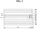
- FIG. 2 is a schematic sectional view taken along line I-I' in FIG. 1 .
- the display device is constructed such that a first base 120, a first buffer layer 130, a thin-film transistor array 140 and an organic light-emitting array 150 are sequentially disposed on the substrate 1000 and such that a protective layer 160 is disposed so as to cover the organic light-emitting array 150.
- a second base 210, a second buffer layer 220 and a touch electrode array 230 are arranged inside a cover glass 3000.
- the touch electrode array 230 is bonded to the protective layer 160, which is disposed on the organic light-emitting array 150, by means of an adhesive layer 400 so as to be opposite the organic light-emitting array 150.
- an active area and a dead area are defined.
- the touch electrode array 230, the organic light-emitting array 150, and the thin-film transistors in the thin-film transistor array 140 excluding the pad portion are formed in the active area.
- a touch pad portion 2350 and the pad portion of the thin-film transistor array 140 are defined in a portion of the dead area.
- first and second bases 120 and 210 serve to prevent damage to the internal arrays during a laser irradiation or etching process.
- the substrate 1000 and the cover glass 3000 are omitted, and the first and second bases 120 and 210 serve to protect the display device from external shocks.
- the first and second bases 120 and 210 may be formed of a polymer material such as, for example, polyimide or photoacryl.
- Each of the first buffer layer 130 and the second buffer layer 220 is formed by sequentially stacking the same type of inorganic films, such as an oxide film (SiO 2 ) or a nitride film (SiN x ), one above another, or by alternately stacking different inorganic films one above another.
- the first and second buffer layers 130 and 220 function as barriers that prevent moisture or outside air from permeating the organic light-emitting array 150 in the subsequent process of bonding the upper substrate to the lower substrate.
- the touch electrode array 230 and the touch pad portion 2350 are formed on the same surface of the second buffer layer 220.
- the touch pad portion 2350 is connected to the pad portion (not illustrated) of the thin-film transistor array 140 by a seal 450 having a conductive ball 455, in a vertical bonding process using the adhesive layer 400.
- the adhesive layer 400 has a moisture permeation preventing function and is directly in contact with the protective layer 160, which covers the organic light-emitting array 150, thereby serving to prevent outside air from entering the organic light-emitting array 150 and to more reliably prevent the permeation of moisture, in addition to the function of the protective layer 160.
- the thin-film transistor array 140 including the pad portion may be configured so as to protrude further than one side of the touch electrode array 230.
- a driving Integrated Circuit (IC) (not illustrated) may be provided on the protruding portion of the thin-film transistor array 140 to transmit signals for driving the touch electrode array, the thin-film transistor array, and the organic light-emitting array.
- a driving pad and a dummy pad include a plurality of dummy electrodes and are connected to the driving IC via wires.
- the driving IC may be bonded to and connected to a flexible printed circuit board (FPCB) (not illustrated), thereby being controlled by a micro control unit (MCU) (not illustrated) and a timing controller (not illustrated) provided in the FPCB.
- the dummy pad is formed in the same layer as the metal that forms a gate line or a data line in the area that corresponds to the touch pad portion 2350 in the dead area around the active area.
- the driving IC may be mounted on the flexible printed circuit board and the FPCB may be boned with the display device using an anisotropic conductive film (ACF). Or, the driving IC may be mounted on the thin-film transistor array 140 using the ACF in a chip-on-film (COF) manner.
- ACF anisotropic conductive film
- the dummy pad and the driving pad of the thin-film transistor array 140 are connected to the flexible printed circuit board.
- the flexible printed circuit board may further include a controller (not illustrated) for controlling the driving IC.
- the dummy pad is formed in the same layer as the metal that forms a gate line or a data line in the area that corresponds to the touch pad portion in the dead area around the active area.
- FIG. 3 is a schematic view illustrating the characteristics of the first mesh electrodes 101 and the second mesh electrodes 102 according to an embodiment.
- the first mesh electrodes 101 include the first and second line electrodes 1011 and 1012, which are arranged in the third and fourth directions so as to intersect each other.
- the second mesh electrodes 102 include the third and fourth line electrodes 1021 and 1022, which are arranged in the third and fourth directions so as to intersect each other.
- the first and second mesh electrodes 101 and 102 may be positioned so as to include portions that overlap the pixel openings 111R, 111G and 111B.
- Each of the pixel openings 111R, 111G and 111B defines a light emitting portion of each of Red, Green, and Blue organic light emitting elements.
- the first and second mesh electrodes 101 and 102 may be divided into overlapping portions, which are positioned so as to overlap the pixel openings 111R, 111G and 111B, and non-overlapping portions, which are positioned so as not to overlap the pixel openings 111R, 111G and 111B. Referring to FIG. 3 , the overlapping portions are the portions that are indicated by cross-shaped dotted lines, and the non-overlapping portions are the remaining portions.
- each of the pixel openings 111R, 111G and 111B is formed in a diamond shape, the embodiment is not limited thereto.
- the pixel openings 111R, 111G and 111B may be formed in various other shapes, such as a rectangular shape, depending on the design.
- lattice portions which are formed by the intersection between the first line electrodes 1011 and the second line electrodes 1012 or the intersection between the third line electrodes 1021 and the fourth line electrodes 1022, may be positioned at the overlapping portions; however, the embodiment is not limited thereto.
- the lattice portions may be positioned at the non-overlapping portions, rather than the overlapping portions, and any one of the first to fourth line electrodes may be positioned so as to pass through the overlapping portions.
- the lattice portions are positioned at the centers of the pixel openings 111R, 111G and 111B, the possibility of the lattice portions being visible to the outside is low even when the viewing angle increases. Therefore, in order to improve the viewing angle characteristics, it is desirable for the lattice portions to be positioned at the centers of the pixel openings 111R, 111G and 111B.
- All or at least some of the overlapping portions include brightness-increasing portions 1005, which are formed of a material different from that of the non-overlapping portions.
- the brightness-increasing portions 1005 are formed of a material different from that of the first to fourth line electrodes 1011, 1012, 1021 and 1022 positioned in the portions other than the brightness-increasing portions 1005, such as the non-overlapping portions.
- the first to fourth line electrodes 1011, 1012, 1021 and 1022, excluding the brightness-increasing portions 1005, may be formed of metal selected from among Cu, Ag, Al, Mo, To and Au, or an alloy thereof, and the brightness-increasing portions 1005 may be formed of a transparent conductive material such as, for example, ITO, IZO, IGZO or ZnO.
- the embodiment is not limited thereto.
- segment electrodes 1007 may be further provided at regions corresponding to the overlapping portions.
- the segment electrodes 1007 are disposed at the positions corresponding to the pixel openings 111R, 111G and 111B and the overlapping portions.
- the segment electrodes 1007 may be formed of a transparent conductive material such as, for example, ITO, IZO, IGZO or ZnO; however, the embodiment is not limited thereto.
- the segment electrodes 1007 may be omitted depending on the design. Since the segment electrodes 1007 are formed of a transparent conductive material, they do not block the pixel openings 111, and compensate for the resistance components of the first and second mesh electrodes 101 and 102.
- the segment electrodes 1007 may be formed of the same material as the brightness-increasing portions 1005 and may be formed integrally therewith.
- the positions and configuration of the brightness-increasing portions 1005 may be variously set depending on the design.
- the brightness-increasing portions 1005 may be formed at the overlapping portions of the first line electrodes 1011 of the first mesh electrodes 101, or may be formed at the overlapping portions of the second line electrodes 1012. Alternatively, the brightness-increasing portions 1005 may be formed at both the overlapping portions of the first line electrodes 1011 and the overlapping portions of the second line electrodes 1012. However, in order to minimize deterioration in resistance-capacitance characteristics, it is desirable that the brightness-increasing portions 1005 be positioned at either the overlapping portions of the first line electrodes 1011 or the overlapping portions of the second line electrodes 1012.
- the brightness-increasing portions 1005 may be formed at the overlapping portions of the third line electrodes 1021 of the second mesh electrodes 102, or may be formed at the overlapping portions of the fourth line electrodes 1022. Alternatively, the brightness-increasing portions 1005 may be formed at both the overlapping portions of the third line electrodes 1021 and the overlapping portions of the fourth line electrodes 1022. However, in order to minimize deterioration in resistance-capacitance characteristics, it is desirable that the brightness-increasing portions 1005 may be positioned at either the overlapping portions of the third line electrodes 1021 or the overlapping portions of the fourth line electrodes 10122.
- one of two neighboring brightness-increasing portions 1005 may be positioned at the overlapping portion of the line electrode that is arranged in the third direction, out of the first to fourth line electrodes, and the other one may be positioned at the overlapping portion of the line electrode that is arranged in the fourth direction. That is, two neighboring brightness-increasing portions 1005 may be arranged in directions different from each other, thereby minimizing deterioration in brightness of the pixel openings 111R, 111G and 111B and improving the viewing angle characteristics.
- the brightness-increasing portion 1005, which is positioned on one pixel opening is formed at the overlapping portion of the first line electrode 1011, which is arranged in the third direction
- the brightness-increasing portion 1005, which is positioned on another neighboring pixel opening may be formed at the overlapping portion of the second line electrode 1012, which is arranged in the fourth direction.
- the brightness-increasing portion 1005, which is positioned on one pixel opening is formed at the overlapping portion of the third line electrode 1021, which is arranged in the third direction
- the brightness-increasing portion 1005, which is positioned on another neighboring pixel opening may be formed at the overlapping portion of the fourth line electrode 1022, which is arranged in the fourth direction.
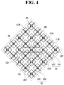
- FIG. 4 is a schematic view illustrating the characteristics of the first mesh electrodes 101 and the second mesh electrodes 102 according to an embodiment.
- the brightness-increasing portions 1005 may be formed at all portions of the first and second mesh electrodes 101 and 102 that overlap the pixel openings 111R, 111G and 111B. However, depending on the design, the brightness-increasing portions 1005 may be formed only at some of the overlapping portions.
- the brightness-increasing portions 1005 may be spaced apart from each other, with the k (where k is a natural number) number of overlapping portions interposed therebetween.
- the overlapping portions including the brightness-increasing portions 1005 may be spaced apart from each other, with the k number of overlapping portions, which include no brightness-increasing portions, interposed therebetween.
- FIG. 5 is a sectional view taken along line II-II' in FIG. 3 to illustrate the cross-sectional structure of the organic light-emitting display device according to an embodiment.
- the first base 120 and the substrate 1000 may be provided below the first buffer layer 130
- the second base 210 and the cover window 3000 may be provided above the second buffer layer 220.
- the thin-film transistor array 140 which includes a thin-film transistor (TFT), is disposed on the first buffer layer 130.
- the thin-film transistor (TFT) includes an active layer 141, which includes a source region 142 and a drain region 143, a gate insulation film 144 and a gate electrode 145, which are disposed on the active layer 141, an interlayer insulation film 148a, which covers the active layer 141 and the gate electrode 145 and has contact holes formed to expose the source and drain regions 142 and 143 therethrough, and a source electrode 146 and a drain electrode 147, which are formed so as to contact the source and drain regions 142 and 143 through the contact holes.
- a first passivation layer 148b is formed on the thin-film transistor (TFT).
- the first passivation layer 148b has a contact hole 149 formed to expose the drain electrode 147 therethrough.
- a first electrode 151 which is connected to the contact hole 149, is disposed on the first passivation layer 148b. Further, a bank insulation film 153, which defines the pixel opening 111 by exposing a portion of the first electrode 151, is disposed on the first passivation layer 148b. A spacer 154 may be further disposed on the bank insulation film 153.
- An organic layer 152 which includes an emission layer, is formed on the first electrode 151.
- the organic layer 152 is divided into an electron injection layer (EIL), an electron transport layer (ETL), an emission layer (EML), a hole transport layer (HTL), and a hole injection layer (HIL).
- the emission layer emits light having a specific wavelength as excitons, which are generated by recombination of electrons from a cathode and holes from an anode, return to the ground state.
- the organic layer 152 may be formed over the entire surface of the buffer layer 130 including the bank insulation film 153 as well as the first electrode 151.
- the embodiment is not limited thereto.
- a second electrode 155 is formed on the organic layer 152.
- the second electrode 155 may be formed over the entire surface of the buffer layer 130 including the organic layer 152.
- the organic light-emitting array 150 is protected from outside moisture by the protective layer 160.
- the protective layer 160 may be formed by alternately stacking inorganic films and organic films. However, the embodiment is not limited thereto.
- the touch electrode array 230 is disposed on the second buffer layer 220.
- the touch electrode array 230 is bonded to the organic light-emitting array 150 by means of the adhesive layer 400 so as to be opposite the organic light-emitting array 150.
- the first to fourth line electrodes 1011, 1012, 1021 and 1022 are disposed on the surface of the second buffer layer 220 that is opposite the organic light-emitting array 150.
- the first to fourth line electrodes 1011, 1012, 1021 and 1022 include overlapping portions that overlap the pixel openings 156.
- FIG. 5 illustrates the overlapping portion of the first line electrode 1011 that overlaps the pixel opening 156.
- Some of the overlapping portions of the first to fourth line electrodes 1011, 1012, 1021 and 1022 are provided with the brightness-increasing portions 1005. Referring to FIG. 5 , it can be seen that the brightness-increasing portion 1005 is also positioned at the overlapping portion of the third line electrode 1021 that overlaps the pixel opening 156.
- the segment electrodes 1007 may be further disposed on the first to fourth line electrodes 1011, 1012, 1021 and 1022.
- the segment electrodes 1007 may be formed of a transparent conductive material.
- the segment electrodes 1007 may be formed of the same material as the brightness-increasing portions 1005, and may be formed integrally therewith.
- the embodiment is not limited thereto.
- no stepped portions are formed between the segment electrodes 1007 and the brightness-increasing portions 1005.
- the process of forming the brightness-increasing portions 1005 may be simplified.
- the segment electrodes 1007 are disposed at positions corresponding to the pixel openings 156, and are disposed below the first to fourth line electrodes 1011, 1012, 1021 and 1022 so as to cover the overlapping portions.
- the segment electrodes 1007 may be formed of the same material and in the same layer as the brightness-increasing portions 1005.
- FIGs. 6 and 7 are sectional views illustrating the cross-sectional structures of the bridges 912 shown in FIGs. 3 and 4 .
- the connecting mesh patterns 1027 are positioned in the same plane as the first and second mesh electrodes 101 and 102 and connect neighboring second mesh electrodes 102 to each other.
- the connecting mesh patterns 1027 connect the neighboring second mesh electrodes 102 to each other via line electrodes 1024 and 1025 that are arranged in the third direction and the fourth direction.
- the connecting mesh patterns 1027 include overlapping portions that overlap the pixel openings 156, and the segment electrodes 1007 are formed at positions corresponding to the overlapping portions.
- at least one of the line electrodes 1024 and 1025 may be further provided with the brightness-increasing portion, thereby further enhancing the brightness.
- a second passivation layer 231 is formed so as to cover the first and second mesh electrodes 101 and 102 and the connecting mesh patterns 1027, and the bridge 912 is formed on the second passivation layer 231.
- the neighboring first mesh patterns 101 are connected to each other by the bridges 912.
- the second passivation layer 231 has contact holes 2311 formed to expose the line electrodes 1011 of the first mesh electrodes 101 therethrough.
- the bridge 912 is connected to the line electrodes 1011 of two neighboring first mesh electrodes 101 through the contact holes 2311, thereby electrically connecting the two neighboring first mesh electrodes 101 to each other.
- the second passivation layer 231 may be formed so as to expose the brightness-increasing portion 1005.
- any one contact hole 2311 may expose the brightness-increasing portion 1005 that may be connected to one end portion of the bridge 912, and another contact hole 2311 may expose the line electrode 1011 that may be connected to an opposite end portion of the bridge 912.
- the bridge 912 may be connected at two opposite end portions thereof to the brightness-increasing portions 1005, or may be connected at two opposite end portions thereof to the line electrodes 1011, or may be connected at one end portion thereof to the brightness-increasing portion 1005 and may be connected at the opposite end portion thereof to the line electrode 1011, thereby electrically connecting the first mesh electrodes 101 to each other.
- the bridge 912 has a structure that is covered with the first passivation layer 232.
- the touch electrode array 230 shown in FIGs. 6 and 7 is bonded to the organic light-emitting array 150 so as to be opposite the same using the adhesive layer 400. Accordingly, in practice, the touch electrode array 230 is arranged in the state of being vertically inverted from the state shown in FIGs. 6 and 7 .
- the first and second mesh electrodes 101 and 102 are arranged so as to overlap the pixel openings 111.
- the mesh electrodes are positioned between the pixel openings.
- the mesh electrodes are positioned to overlap the sides of the pixel openings.
- the mesh electrodes block the sides of the pixel openings, thereby causing asymmetry of the viewing angle.
- the first and second mesh electrodes 101 and 102 may be positioned so as to overlap the centers of the pixel openings 111. As a result of the first and second mesh electrodes 101 and 102 being positioned at the centers of the pixel openings 111, asymmetry of the viewing angle is prevented.
- first and second mesh electrodes 101 and 102 are slightly misaligned sideways from the centers of the pixel openings 111, the possibility of occurrence of asymmetry of the viewing angle is much lower than the case in which the mesh electrodes block the sides of the pixel openings 111.
- the organic light-emitting display device has a high process margin compared to the related art, in which the mesh electrodes are positioned between the pixel openings 111.
- the in-cell touch organic light-emitting display device has an effect of reducing the degree of asymmetry of the viewing angle attributable to error in the process of aligning the first and second mesh electrodes 101 and 102.
- the brightness-increasing portions 1005 are provided at the overlapping portions of the first and second mesh electrodes 101 and 102. Since the brightness-increasing portions 1005 are formed of a transparent conductive material, they have an effect of minimizing deterioration in brightness attributable to the first and second mesh electrodes 101 and 102 overlapping the pixel openings 111.
- Table 1 shows the comparison results between the vertical color viewing angle and the horizontal color viewing angle of the organic light-emitting display device according to the embodiments and those of the related art, in which mesh electrodes do not overlap pixel openings. Even though results different from the following results may be derived in accordance with a difference in processing, the possibility of occurrence of deviation of the viewing angle during processing and the degree of deviation of the viewing angle can be estimated by comparing the maximum deviations measured in the experiment.
- the degree of asymmetry of the color viewing angle is considered large.
- the maximum deviation of the horizontal color viewing angle is 6° and the maximum deviation of the vertical color viewing angle is 7°. That is, the related art has a problem in that the degree of asymmetry of the color viewing angle is very large even when a processing error is small, and consequently deterioration in the image quality occurs.
- the maximum deviation of the horizontal color viewing angle is only 3°, and the maximum deviation of the vertical color viewing angle is only 4.5°. That is, a processing error, if any, has less influence on deviation of the viewing angle.
- first and second mesh electrodes are positioned so as to overlap pixel openings, it is possible to reduce the degree of asymmetry of a viewing angle attributable to error in the process of aligning the first and second mesh electrodes.
- brightness-increasing portions are provided at overlapping portions of the first and second mesh electrodes. Since the brightness-increasing portions are formed of a transparent conductive material, they have an effect of minimizing deterioration in brightness attributable to the first and second mesh electrodes overlapping the pixel openings.
- the organic light-emitting display device according to any previous clause, wherein the device is an in-cell touch organic light-emitting display device.
Landscapes
- Engineering & Computer Science (AREA)
- General Engineering & Computer Science (AREA)
- Theoretical Computer Science (AREA)
- Physics & Mathematics (AREA)
- Human Computer Interaction (AREA)
- General Physics & Mathematics (AREA)
- Optics & Photonics (AREA)
- Microelectronics & Electronic Packaging (AREA)
- Electroluminescent Light Sources (AREA)
- Devices For Indicating Variable Information By Combining Individual Elements (AREA)
Abstract
Description
- The present disclosure relates to an organic light-emitting display device, and more particularly to an organic light-emitting display device including a metal mesh pattern.
- An image display device, which realizes various pieces of information on a screen, is a core technology of the information and communication age, and is being developed in the direction of becoming thinner, lighter, more portable, and having higher performance. As a flat panel display device that is capable of overcoming the problems of disadvantageous weight and volume of a cathode ray tube (CRT), for example, an organic light-emitting display device, which displays an image by controlling the intensity of luminescence of an organic emission layer, is attracting attention.
- The organic light-emitting display device described above uses a self-illuminating organic light-emitting element, and therefore does not require a separate light source and enables realization of a super-thin-type display. In recent years, research on a touch-panel-integrated display device having an in-cell touch structure, which uses an organic light-emitting element and includes a touch electrode array inside a light-emitting cell, has been actively conducted.
- A touch panel includes a first touch electrode, which is arranged in a first direction, and a second touch electrode, which is arranged in a second direction so as to intersect the first touch electrode. The first touch electrode and the second touch electrode are electrically isolated from each other. In this state, when an object charged with static electricity is brought into contact with the touch panel, the touch panel detects a touch input by sensing the change of mutual capacitance between the first touch electrode and the second touch electrode.
- In manufacturing an organic light-emitting display device having a flexible touch structure, research is being actively conducted into the application of a metal mesh electrode, having superior flexibility and low resistance characteristics, to a touch electrode.
- However, because the metal mesh electrode has higher reflectivity than a transparent conductive material, it has a high possibility of being visible to the outside and deteriorates the overall brightness of the organic light-emitting display device.
- To solve this problem, a method of aligning a metal mesh electrode with a bank, which is a non-light-emitting region, has been devised. However, there is a high possibility of occurrence of misalignment during a process of accurately aligning a mesh electrode with a display panel. If this misalignment occurs, as a viewing angle increases, the mesh electrode blocks a portion of a pixel opening, which causes asymmetry of a vertical viewing angle or a horizontal viewing angle.
- Accordingly, the present disclosure is directed to an organic light-emitting display device that substantially addresses one or more problems due to limitations and disadvantages of the related art.
- The present disclosure seeks to provide an organic light-emitting display device, which has improved color viewing angle characteristics while including a mesh pattern.
- Aspects of an invention are defined in the appended independent claims.
- Additional aspects, advantages, and features of embodiments will be set forth in part in the description which follows and in part will become apparent to those having ordinary skill in the art upon examination of the following or may be learned from practice of the present disclosure. The advantages of the present disclosure may be realized and attained by the structure particularly pointed out in the written description and claims hereof as well as the appended drawings.
- In accordance with the present disclosure, as embodied and broadly described herein, an organic light-emitting display device includes an organic light-emitting array including a plurality of pixel openings, and a touch electrode array bonded to the organic light-emitting array. The touch electrode array includes a plurality of first mesh electrodes arranged in a first direction and having a structure having multiple lattice portions, and a plurality of second mesh electrodes arranged in a second direction and having a structure having multiple lattice portions.
- Each of the first mesh electrodes and the second mesh electrodes may include a plurality of overlapping portions that overlap the pixel openings and a plurality of non-overlapping portions positioned between the pixel openings.
- At least some of the overlapping portions may include brightness-increasing portions, which are formed of a material different from that of the non-overlapping portions. At this time, the lattice portions may be positioned on the pixel openings so as to overlap the pixel openings. The brightness-increasing portions may include at least one of two line electrodes that form each lattice portion. The brightness-increasing portions may be formed of a transparent conductive material.
- It is to be understood that both the foregoing general description and the following detailed description of the present disclosure are exemplary and explanatory only and are intended to provide further explanation of the present disclosure as claimed.
- The accompanying drawings, which are included to provide a further understanding of the present disclosure and are incorporated in and constitute a part of this application, illustrate embodiment(s) and together with the description serve to explain the principles of the present disclosure.
-
FIG. 1 is a plan view illustrating an organic light-emitting display device according to an embodiment. -
FIG. 2 is a schematic sectional view taken along line I-I' inFIG. 1 . -
FIG. 3 is a schematic view illustrating the characteristics of first mesh electrodes and second mesh electrodes according to an embodiment. -
FIG. 4 is a schematic view illustrating the characteristics of first mesh electrodes and second mesh electrodes according to an embodiment. -
FIG. 5 is a sectional view taken along line II-II' inFIG. 3 . -
FIG. 6 is a sectional view illustrating the cross-sectional structure according to an embodiment of bridges shown inFIG. 3 . -
FIG. 7 is a sectional view illustrating the cross-sectional structure according to an embodiment of bridges shown inFIG. 4 . - Hereinafter, exemplary embodiments will be described with reference to the accompanying drawings. Wherever possible, the same reference numbers will be used throughout the drawings to refer to the same or like parts. In addition, in the following description of the embodiments, a detailed description of known functions and configurations incorporated herein will be omitted when it may make the subject matter of the present disclosure unclear. Also, the terms of constituent elements used in the following description are defined taking into consideration ease in the preparation of the specification, and may differ from the terms used to describe elements of actual products.
- In the description related to a positional relationship, for example, when an element is referred to as being "on", "above", "under" or "beside" another element, it can be directly on the other element, or intervening elements may also be present.
- It will be understood that although the terms "first", "second", "third", etc., may be used herein to describe various elements, these elements should not be limited by these terms. These terms are only used to distinguish one element from another element. Thus, a first element discussed below could be termed a second element without departing from the teachings of example embodiments.
- In the drawings, the size and thickness of each constituent element are illustrated merely for convenience of description, and the present disclosure is not necessarily limited to the illustrated size and thickness of each constituent element.
- Hereinafter, various embodiments will be described with reference to the accompanying drawings.
-
FIG. 1 is a plan view for explaining an organic light-emitting display device according to an embodiment. - An organic light-emitting display device according to an embodiment includes a plurality of
first mesh electrodes 101, which are arranged on asubstrate 1000 in a first direction, and a plurality ofsecond mesh electrodes 102, which are arranged in a second direction, which intersects the first direction. In this embodiment, the first direction is defined as the horizontal direction and the second direction is defined as the vertical direction; however, the embodiment is not limited thereto. - Each of the
first mesh electrodes 101 and thesecond mesh electrodes 102 has a multiple-lattice structure. Each of thefirst mesh electrodes 101 includes a plurality offirst line electrodes 1011, which are formed lengthwise in a third direction, and a plurality ofsecond line electrodes 1012, which are formed lengthwise in a fourth direction and intersect thefirst line electrodes 1011 so as to form the lattice structure. - Each of the
second mesh electrodes 102 includes a plurality ofthird line electrodes 1021, which are formed lengthwise in the third direction, and a plurality offourth line electrodes 1022, which are formed lengthwise in the fourth direction and intersect thethird line electrodes 1021 so as to form the lattice structure. - The
first mesh electrodes 101, which are arranged adjacent to each other in the first direction, are connected to each other viabridges 912. Thesecond mesh electrodes 102, which are arranged adjacent to each other in the second direction, are connected to each other via connectingmesh patterns 1027. Here, thefirst mesh electrodes 101 connected via thebridges 912 may serve as driving electrodes that apply a driving signal for sensing a touch signal and thesecond mesh electrodes 102 connected via the connectingmesh patterns 1027 may serve as sensing electrodes that sense a touch signal, or vice versa; however, the embodiment is not limited thereto. - The concrete structures of the first and
second mesh electrodes - The
first mesh electrodes 101, which are positioned at the outermost portion of a display area A/A, are connected topad electrodes 110 of atouch pad portion 2350 viafirst routing lines 913a, and thesecond mesh electrodes 102, which are positioned at the outermost portion of the display area A/A, are connected to thepad electrodes 110 of thetouch pad portion 2350 viasecond routing lines 913b. -
FIG. 2 is a schematic sectional view taken along line I-I' inFIG. 1 . - The display device according to the embodiment is constructed such that a
first base 120, afirst buffer layer 130, a thin-film transistor array 140 and an organic light-emitting array 150 are sequentially disposed on thesubstrate 1000 and such that aprotective layer 160 is disposed so as to cover the organic light-emitting array 150. Asecond base 210, asecond buffer layer 220 and atouch electrode array 230 are arranged inside acover glass 3000. Thetouch electrode array 230 is bonded to theprotective layer 160, which is disposed on the organic light-emittingarray 150, by means of anadhesive layer 400 so as to be opposite the organic light-emitting array 150. - In each of the
first buffer layer 130 and thesecond buffer layer 220, an active area and a dead area are defined. Thetouch electrode array 230, the organic light-emittingarray 150, and the thin-film transistors in the thin-film transistor array 140 excluding the pad portion are formed in the active area. In addition, atouch pad portion 2350 and the pad portion of the thin-film transistor array 140 are defined in a portion of the dead area. - Here, the first and
second bases substrate 1000 and thecover glass 3000 are omitted, and the first andsecond bases second bases - Each of the
first buffer layer 130 and thesecond buffer layer 220 is formed by sequentially stacking the same type of inorganic films, such as an oxide film (SiO2) or a nitride film (SiNx), one above another, or by alternately stacking different inorganic films one above another. The first and second buffer layers 130 and 220 function as barriers that prevent moisture or outside air from permeating the organic light-emittingarray 150 in the subsequent process of bonding the upper substrate to the lower substrate. - The
touch electrode array 230 and thetouch pad portion 2350 are formed on the same surface of thesecond buffer layer 220. Thetouch pad portion 2350 is connected to the pad portion (not illustrated) of the thin-film transistor array 140 by aseal 450 having aconductive ball 455, in a vertical bonding process using theadhesive layer 400. At this time, theadhesive layer 400 has a moisture permeation preventing function and is directly in contact with theprotective layer 160, which covers the organic light-emittingarray 150, thereby serving to prevent outside air from entering the organic light-emittingarray 150 and to more reliably prevent the permeation of moisture, in addition to the function of theprotective layer 160. - Here, the thin-
film transistor array 140 including the pad portion may be configured so as to protrude further than one side of thetouch electrode array 230. A driving Integrated Circuit (IC) (not illustrated) may be provided on the protruding portion of the thin-film transistor array 140 to transmit signals for driving the touch electrode array, the thin-film transistor array, and the organic light-emitting array. Although not illustrated, with regard to the driving IC and the thin-film transistor array, a driving pad and a dummy pad include a plurality of dummy electrodes and are connected to the driving IC via wires. In addition, after glass removal, the driving IC may be bonded to and connected to a flexible printed circuit board (FPCB) (not illustrated), thereby being controlled by a micro control unit (MCU) (not illustrated) and a timing controller (not illustrated) provided in the FPCB. The dummy pad is formed in the same layer as the metal that forms a gate line or a data line in the area that corresponds to thetouch pad portion 2350 in the dead area around the active area. - The driving IC may be mounted on the flexible printed circuit board and the FPCB may be boned with the display device using an anisotropic conductive film (ACF). Or, the driving IC may be mounted on the thin-
film transistor array 140 using the ACF in a chip-on-film (COF) manner. - Although not illustrated, the dummy pad and the driving pad of the thin-
film transistor array 140 are connected to the flexible printed circuit board. In addition, the flexible printed circuit board may further include a controller (not illustrated) for controlling the driving IC. - The dummy pad is formed in the same layer as the metal that forms a gate line or a data line in the area that corresponds to the touch pad portion in the dead area around the active area.
-
FIG. 3 is a schematic view illustrating the characteristics of thefirst mesh electrodes 101 and thesecond mesh electrodes 102 according to an embodiment. - The
first mesh electrodes 101, as described above, include the first andsecond line electrodes second mesh electrodes 102 include the third andfourth line electrodes - The first and
second mesh electrodes pixel openings pixel openings second mesh electrodes pixel openings pixel openings FIG. 3 , the overlapping portions are the portions that are indicated by cross-shaped dotted lines, and the non-overlapping portions are the remaining portions. - Although it is illustrated in
FIG. 3 that each of thepixel openings pixel openings - As shown in
FIG. 3 , lattice portions, which are formed by the intersection between thefirst line electrodes 1011 and thesecond line electrodes 1012 or the intersection between thethird line electrodes 1021 and thefourth line electrodes 1022, may be positioned at the overlapping portions; however, the embodiment is not limited thereto. The lattice portions may be positioned at the non-overlapping portions, rather than the overlapping portions, and any one of the first to fourth line electrodes may be positioned so as to pass through the overlapping portions. - At this time, in the case in which the lattice portions are positioned at the centers of the
pixel openings pixel openings - All or at least some of the overlapping portions include brightness-increasing
portions 1005, which are formed of a material different from that of the non-overlapping portions. The brightness-increasingportions 1005 are formed of a material different from that of the first tofourth line electrodes portions 1005, such as the non-overlapping portions. - For example, the first to
fourth line electrodes portions 1005, may be formed of metal selected from among Cu, Ag, Al, Mo, To and Au, or an alloy thereof, and the brightness-increasingportions 1005 may be formed of a transparent conductive material such as, for example, ITO, IZO, IGZO or ZnO. However, the embodiment is not limited thereto. - Although the illustration is omitted from
FIG. 1 for convenience,segment electrodes 1007 may be further provided at regions corresponding to the overlapping portions. Thesegment electrodes 1007 are disposed at the positions corresponding to thepixel openings segment electrodes 1007 may be formed of a transparent conductive material such as, for example, ITO, IZO, IGZO or ZnO; however, the embodiment is not limited thereto. Thesegment electrodes 1007 may be omitted depending on the design. Since thesegment electrodes 1007 are formed of a transparent conductive material, they do not block the pixel openings 111, and compensate for the resistance components of the first andsecond mesh electrodes - In the case in which the
segment electrodes 1007 are positioned on the overlapping portions, thesegment electrodes 1007 may be formed of the same material as the brightness-increasingportions 1005 and may be formed integrally therewith. - The brightness-increasing
portions 1005, which are formed of a transparent conductive material, have higher resistance characteristics than the non-overlapping portions, which are formed of metal. Therefore, in the case in which an excessively large number of the brightness-increasingportions 1005 are provided, the touch-sensing performance may be degraded. The positions and configuration of the brightness-increasingportions 1005 may be variously set depending on the design. - The brightness-increasing
portions 1005 may be formed at the overlapping portions of thefirst line electrodes 1011 of thefirst mesh electrodes 101, or may be formed at the overlapping portions of thesecond line electrodes 1012. Alternatively, the brightness-increasingportions 1005 may be formed at both the overlapping portions of thefirst line electrodes 1011 and the overlapping portions of thesecond line electrodes 1012. However, in order to minimize deterioration in resistance-capacitance characteristics, it is desirable that the brightness-increasingportions 1005 be positioned at either the overlapping portions of thefirst line electrodes 1011 or the overlapping portions of thesecond line electrodes 1012. Similarly, the brightness-increasingportions 1005 may be formed at the overlapping portions of thethird line electrodes 1021 of thesecond mesh electrodes 102, or may be formed at the overlapping portions of thefourth line electrodes 1022. Alternatively, the brightness-increasingportions 1005 may be formed at both the overlapping portions of thethird line electrodes 1021 and the overlapping portions of thefourth line electrodes 1022. However, in order to minimize deterioration in resistance-capacitance characteristics, it is desirable that the brightness-increasingportions 1005 may be positioned at either the overlapping portions of thethird line electrodes 1021 or the overlapping portions of the fourth line electrodes 10122. - At this time, one of two neighboring brightness-increasing
portions 1005 may be positioned at the overlapping portion of the line electrode that is arranged in the third direction, out of the first to fourth line electrodes, and the other one may be positioned at the overlapping portion of the line electrode that is arranged in the fourth direction. That is, two neighboring brightness-increasingportions 1005 may be arranged in directions different from each other, thereby minimizing deterioration in brightness of thepixel openings - For example, in the
first mesh electrode 101, when the brightness-increasingportion 1005, which is positioned on one pixel opening, is formed at the overlapping portion of thefirst line electrode 1011, which is arranged in the third direction, the brightness-increasingportion 1005, which is positioned on another neighboring pixel opening, may be formed at the overlapping portion of thesecond line electrode 1012, which is arranged in the fourth direction. - Further, in the
second mesh electrode 102, when the brightness-increasingportion 1005, which is positioned on one pixel opening, is formed at the overlapping portion of thethird line electrode 1021, which is arranged in the third direction, the brightness-increasingportion 1005, which is positioned on another neighboring pixel opening, may be formed at the overlapping portion of thefourth line electrode 1022, which is arranged in the fourth direction. -
FIG. 4 is a schematic view illustrating the characteristics of thefirst mesh electrodes 101 and thesecond mesh electrodes 102 according to an embodiment. - The brightness-increasing
portions 1005 may be formed at all portions of the first andsecond mesh electrodes pixel openings portions 1005 may be formed only at some of the overlapping portions. - Particularly, as shown in
FIG. 4 , the brightness-increasingportions 1005 may be spaced apart from each other, with the k (where k is a natural number) number of overlapping portions interposed therebetween. In other words, the overlapping portions including the brightness-increasingportions 1005 may be spaced apart from each other, with the k number of overlapping portions, which include no brightness-increasing portions, interposed therebetween. -
FIG. 5 is a sectional view taken along line II-II' inFIG. 3 to illustrate the cross-sectional structure of the organic light-emitting display device according to an embodiment. Although the illustration of the structure below thefirst buffer layer 130 and the structure above thesecond buffer layer 220 is omitted from the drawings for convenience, as shown inFIG. 2 , thefirst base 120 and thesubstrate 1000 may be provided below thefirst buffer layer 130, and thesecond base 210 and thecover window 3000 may be provided above thesecond buffer layer 220. - The thin-
film transistor array 140, which includes a thin-film transistor (TFT), is disposed on thefirst buffer layer 130. The thin-film transistor (TFT) includes anactive layer 141, which includes asource region 142 and adrain region 143, agate insulation film 144 and agate electrode 145, which are disposed on theactive layer 141, aninterlayer insulation film 148a, which covers theactive layer 141 and thegate electrode 145 and has contact holes formed to expose the source and drainregions source electrode 146 and adrain electrode 147, which are formed so as to contact the source and drainregions first passivation layer 148b is formed on the thin-film transistor (TFT). Thefirst passivation layer 148b has acontact hole 149 formed to expose thedrain electrode 147 therethrough. - A
first electrode 151, which is connected to thecontact hole 149, is disposed on thefirst passivation layer 148b. Further, abank insulation film 153, which defines the pixel opening 111 by exposing a portion of thefirst electrode 151, is disposed on thefirst passivation layer 148b. Aspacer 154 may be further disposed on thebank insulation film 153. - An
organic layer 152, which includes an emission layer, is formed on thefirst electrode 151. Here, theorganic layer 152 is divided into an electron injection layer (EIL), an electron transport layer (ETL), an emission layer (EML), a hole transport layer (HTL), and a hole injection layer (HIL). The emission layer emits light having a specific wavelength as excitons, which are generated by recombination of electrons from a cathode and holes from an anode, return to the ground state. - The
organic layer 152 may be formed over the entire surface of thebuffer layer 130 including thebank insulation film 153 as well as thefirst electrode 151. However, the embodiment is not limited thereto. - A
second electrode 155 is formed on theorganic layer 152. Thesecond electrode 155 may be formed over the entire surface of thebuffer layer 130 including theorganic layer 152. - The organic light-emitting
array 150 is protected from outside moisture by theprotective layer 160. Theprotective layer 160 may be formed by alternately stacking inorganic films and organic films. However, the embodiment is not limited thereto. - The
touch electrode array 230 is disposed on thesecond buffer layer 220. Thetouch electrode array 230 is bonded to the organic light-emittingarray 150 by means of theadhesive layer 400 so as to be opposite the organic light-emittingarray 150. - Described in more detail, the first to
fourth line electrodes second buffer layer 220 that is opposite the organic light-emittingarray 150. At this time, the first tofourth line electrodes pixel openings 156.FIG. 5 illustrates the overlapping portion of thefirst line electrode 1011 that overlaps thepixel opening 156. Some of the overlapping portions of the first tofourth line electrodes portions 1005. Referring toFIG. 5 , it can be seen that the brightness-increasingportion 1005 is also positioned at the overlapping portion of thethird line electrode 1021 that overlaps thepixel opening 156. - Referring to
FIG. 5 , thesegment electrodes 1007 may be further disposed on the first tofourth line electrodes segment electrodes 1007 may be formed of a transparent conductive material. As shown inFIG. 5 , thesegment electrodes 1007 may be formed of the same material as the brightness-increasingportions 1005, and may be formed integrally therewith. However, the embodiment is not limited thereto. In the case in which thesegment electrodes 1007 and the brightness-increasingportions 1005 are formed integrally with each other, no stepped portions are formed between thesegment electrodes 1007 and the brightness-increasingportions 1005. As such, by forming thesegment electrodes 1007 and the brightness-increasingportions 1005 at the same time, the process of forming the brightness-increasingportions 1005 may be simplified. - The
segment electrodes 1007 are disposed at positions corresponding to thepixel openings 156, and are disposed below the first tofourth line electrodes portions 1005 are provided, thesegment electrodes 1007 may be formed of the same material and in the same layer as the brightness-increasingportions 1005. -
FIGs. 6 and 7 are sectional views illustrating the cross-sectional structures of thebridges 912 shown inFIGs. 3 and4 . - As described above, the connecting
mesh patterns 1027 are positioned in the same plane as the first andsecond mesh electrodes second mesh electrodes 102 to each other. The connectingmesh patterns 1027 connect the neighboringsecond mesh electrodes 102 to each other vialine electrodes mesh patterns 1027 include overlapping portions that overlap thepixel openings 156, and thesegment electrodes 1007 are formed at positions corresponding to the overlapping portions. Depending on the embodiment, within the region at which the connectingmesh patterns 1027 overlap the pixel openings, at least one of theline electrodes - A
second passivation layer 231 is formed so as to cover the first andsecond mesh electrodes mesh patterns 1027, and thebridge 912 is formed on thesecond passivation layer 231. The neighboringfirst mesh patterns 101 are connected to each other by thebridges 912. - Referring to
Fig. 6 , thesecond passivation layer 231 hascontact holes 2311 formed to expose theline electrodes 1011 of thefirst mesh electrodes 101 therethrough. Thebridge 912 is connected to theline electrodes 1011 of two neighboringfirst mesh electrodes 101 through the contact holes 2311, thereby electrically connecting the two neighboringfirst mesh electrodes 101 to each other. - Meanwhile, the
second passivation layer 231, as shown inFIG. 7 , may be formed so as to expose the brightness-increasingportion 1005. Specifically, any onecontact hole 2311 may expose the brightness-increasingportion 1005 that may be connected to one end portion of thebridge 912, and anothercontact hole 2311 may expose theline electrode 1011 that may be connected to an opposite end portion of thebridge 912. Thebridge 912 may be connected at two opposite end portions thereof to the brightness-increasingportions 1005, or may be connected at two opposite end portions thereof to theline electrodes 1011, or may be connected at one end portion thereof to the brightness-increasingportion 1005 and may be connected at the opposite end portion thereof to theline electrode 1011, thereby electrically connecting thefirst mesh electrodes 101 to each other. - The
bridge 912 has a structure that is covered with thefirst passivation layer 232. - The
touch electrode array 230 shown inFIGs. 6 and 7 is bonded to the organic light-emittingarray 150 so as to be opposite the same using theadhesive layer 400. Accordingly, in practice, thetouch electrode array 230 is arranged in the state of being vertically inverted from the state shown inFIGs. 6 and 7 . - In the above-described organic light-emitting display device according to the embodiments, the first and
second mesh electrodes - In the related art, the mesh electrodes are positioned between the pixel openings. However, in this structure, if an error occurs during an aligning process, the mesh electrodes are positioned to overlap the sides of the pixel openings. Thus, the mesh electrodes block the sides of the pixel openings, thereby causing asymmetry of the viewing angle. On the other hand, according to the embodiments, the first and
second mesh electrodes second mesh electrodes - Even if the first and
second mesh electrodes - Accordingly, the organic light-emitting display device according to the embodiments has a high process margin compared to the related art, in which the mesh electrodes are positioned between the pixel openings 111. As a result, the in-cell touch organic light-emitting display device according to the embodiments has an effect of reducing the degree of asymmetry of the viewing angle attributable to error in the process of aligning the first and
second mesh electrodes - In addition, in order to minimize deterioration in brightness attributable to the first and
second mesh electrodes portions 1005 are provided at the overlapping portions of the first andsecond mesh electrodes portions 1005 are formed of a transparent conductive material, they have an effect of minimizing deterioration in brightness attributable to the first andsecond mesh electrodes - Specifically, it is possible to minimize deterioration in brightness and resistance by positioning the brightness-increasing
portion 1005 at only one of two line electrodes positioned on the pixel opening 111. - The following Table 1 shows the comparison results between the vertical color viewing angle and the horizontal color viewing angle of the organic light-emitting display device according to the embodiments and those of the related art, in which mesh electrodes do not overlap pixel openings. Even though results different from the following results may be derived in accordance with a difference in processing, the possibility of occurrence of deviation of the viewing angle during processing and the degree of deviation of the viewing angle can be estimated by comparing the maximum deviations measured in the experiment.
Table 1 Deviation of Horizontal Color Viewing Angle Deviation of Vertical Color Viewing Angle Prior Art 6° (Maximum Deviation Measured in Experiment) 7° (Maximum Deviation Measured in Experiment) Present Disclosure 3° (Maximum Deviation Measured in Experiment) 4.5° (Maximum Deviation Measured in Experiment) - In the in-cell touch organic light-emitting display device, if the deviation of the viewing angle is 5° or more, the degree of asymmetry of the color viewing angle is considered large.
- According to the above experimental results, in the organic light-emitting display device of the related art, the maximum deviation of the horizontal color viewing angle is 6° and the maximum deviation of the vertical color viewing angle is 7°. That is, the related art has a problem in that the degree of asymmetry of the color viewing angle is very large even when a processing error is small, and consequently deterioration in the image quality occurs.
- On the other hand, in the organic light-emitting display device according to the embodiments, the maximum deviation of the horizontal color viewing angle is only 3°, and the maximum deviation of the vertical color viewing angle is only 4.5°. That is, a processing error, if any, has less influence on deviation of the viewing angle.
- As is apparent from the above description, in an organic light-emitting display device according to the embodiments, since first and second mesh electrodes are positioned so as to overlap pixel openings, it is possible to reduce the degree of asymmetry of a viewing angle attributable to error in the process of aligning the first and second mesh electrodes.
- In addition, in order to minimize deterioration in brightness attributable to the first and second mesh electrodes being positioned on the pixel openings, brightness-increasing portions are provided at overlapping portions of the first and second mesh electrodes. Since the brightness-increasing portions are formed of a transparent conductive material, they have an effect of minimizing deterioration in brightness attributable to the first and second mesh electrodes overlapping the pixel openings.
- It will be apparent to those skilled in the art that various modifications and variations can be made to the embodiments without departing from the scope of the appended claims. Thus, it is intended that the present disclosure covers all modifications and variations provided they come within the scope of the appended claims.
- Further embodiments are defined in the following numbered clauses:
- 1. An organic light-emitting display device comprising: an organic light-emitting array including a plurality of pixel openings arranged in a matrix form; and a touch electrode array bonded to the organic light-emitting array, wherein the touch electrode array includes a plurality of first mesh electrodes arranged in a first direction and having a structure having multiple lattice portions, and a plurality of second mesh electrodes insulated from the first mesh electrodes and arranged in a second direction intersecting the first direction and having a structure having multiple lattice portions, wherein each of the first mesh electrodes and the second mesh electrodes includes a plurality of overlapping portions positioned on the pixel openings so as to overlap the pixel openings, and a plurality of non-overlapping portions positioned between the pixel openings, and wherein at least some of the overlapping portions include brightness-increasing portions, the brightness-increasing portions being formed of a material different from that of the non-overlapping portions.
- 2. The organic light-emitting display device according to clause 1, wherein the lattice portions of the first mesh electrodes and the second mesh electrodes are positioned on the pixel openings so as to overlap the pixel openings.
- 3. The organic light-emitting display device according to clause 2, wherein: the first mesh electrodes include a plurality of first line electrodes and a plurality of second line electrodes, arranged in a third direction and a fourth direction so as to intersect each other and to form a lattice structure, the second mesh electrodes include a plurality of third line electrodes and a plurality of fourth line electrodes, arranged in the third direction and the fourth direction so as to intersect each other and to form a lattice structure, and the brightness-increasing portions include portions positioned at the overlapping portions of at least one of the first line electrodes and the second line electrodes.
- 4. The organic light-emitting display device according to clause 1, wherein the brightness-increasing portions are formed of a transparent conductive material.
- 5. The organic light-emitting display device according to clause 1, further comprising: bridges positioned in a different layer from the first mesh electrodes and the second mesh electrodes and configured to electrically connect the first mesh electrodes, arranged adjacent to each other in the first direction, to each other through contact holes; and connecting mesh patterns positioned in a same layer as the first mesh electrodes and the second mesh electrodes and configured to connect the second mesh electrodes, arranged adjacent to each other in the second direction, to each other.
- 6. The organic light-emitting display device according to clause 5, further comprising: brightness-increasing portions positioned at portions of the connecting mesh patterns that overlap the pixel openings.
- 7. The organic light-emitting display device according to clause 3, further comprising: segment electrodes positioned corresponding to the pixel openings.
- 8. The organic light-emitting display device according to clause 7, wherein the segment electrodes are formed of a transparent conductive material.
- 9. The organic light-emitting display device according to clause 7, wherein the brightness-increasing portions and the segment electrodes are simultaneously formed of a same transparent conductive material as each other.
- 10. The organic light-emitting display device according to clause 1, wherein among the overlapping portions, the overlapping portions including the brightness-increasing portions are spaced apart from each other, with a k (where k is a natural number) number of overlapping portions interposed therebetween.
- 11. The organic light-emitting display device according to clause 3, wherein among the brightness-increasing portions, one of two neighboring brightness-increasing portions includes a portion positioned at an overlapping portion of a line electrode that is arranged in the third direction out of the first to fourth line electrodes, and a remaining one includes a portion positioned at an overlapping portion of a line electrode that is arranged in the fourth direction.
- The organic light-emitting display device according to any previous clause, wherein the device is an in-cell touch organic light-emitting display device.
Claims (12)
- An organic light-emitting display device comprising:an organic light-emitting array (150) including a plurality of pixel openings (111R, 111G, 111B) arranged in a matrix form; anda touch electrode array (230) bonded to the organic light-emitting array (150),wherein the touch electrode array (150) includes a plurality of first mesh electrodes (101) arranged in a first direction and having a structure having multiple lattice portions, and a plurality of second mesh electrodes (102) insulated from the first mesh electrodes and arranged in a second direction intersecting the first direction and having a structure having multiple lattice portions,wherein each of the first mesh electrodes (101) and the second mesh electrodes (102) includes a plurality of overlapping portions positioned on the pixel openings (111R, 111G, 111B) so as to overlap the pixel openings, and a plurality of non-overlapping portions positioned between the pixel openings (111R, 111G, 111B, andwherein at least some of the overlapping portions include brightness-increasing portions (1005), the brightness-increasing portions being formed of a material different from that of the non-overlapping portions.
- The organic light-emitting display device according to claim 1, wherein the lattice portions of the first mesh electrodes (101) and the second mesh electrodes (102) are positioned on the pixel openings (111R, 111G, 111B) so as to overlap the pixel openings.
- The organic light-emitting display device according to claim 1 or claim 2, wherein:the first mesh electrodes (101) include a plurality of first line electrodes (1011) and a plurality of second line electrodes (1012), arranged in a third direction and a fourth direction so as to intersect each other and to form a lattice structure,the second mesh electrodes (102) include a plurality of third line electrodes (1021) and a plurality of fourth line electrodes (1022), arranged in the third direction and the fourth direction so as to intersect each other and to form a lattice structure, andthe brightness-increasing portions (1005) include portions positioned at the overlapping portions of at least one of the first line electrodes (1011) and the second line electrodes (1012).
- The organic light-emitting display device according to claim 3, further comprising:segment electrodes (1007) positioned corresponding to the pixel openings (111R, 111G, 111B).
- The organic light-emitting display device according to claim 4, wherein the segment electrodes (1007) are formed of a transparent conductive material.
- The organic light-emitting display device according to claim 4 or claim 5, wherein the brightness-increasing portions (1005) and the segment electrodes (1007) are simultaneously formed of a same transparent conductive material as each other.
- The organic light-emitting display device according to claim 3, 4, 5 or 6, wherein among the brightness-increasing portions (1005),
one of two neighboring brightness-increasing portions (1005) includes a portion positioned at an overlapping portion of a line electrode that is arranged in the third direction out of the first to fourth line electrodes, and
a remaining one includes a portion positioned at an overlapping portion of a line electrode that is arranged in the fourth direction. - The organic light-emitting display device according to any preceding claim, wherein the brightness-increasing portions (1005) are formed of a transparent conductive material.
- The organic light-emitting display device according to any preceding claim, further comprising:bridges (912) positioned in a different layer from the first mesh electrodes (101) and the second mesh electrodes (102) and configured to electrically connect the first mesh electrodes (101), arranged adjacent to each other in the first direction, to each other through contact holes; andconnecting mesh patterns positioned in a same layer as the first mesh electrodes (101) and the second mesh electrodes (102) and configured to connect the second mesh electrodes (102), arranged adjacent to each other in the second direction, to each other.
- The organic light-emitting display device according to claim 9, further comprising:brightness-increasing portions (1005) positioned at portions of the connecting mesh patterns that overlap the pixel openings (111R, 111G, 111B).
- The organic light-emitting display device according to any preceding claim, wherein the brightness-increasing portions (1005) are formed only at some of the overlapping portions.
- The organic light-emitting display device according to any preceding claim, wherein among the overlapping portions, the overlapping portions including the brightness-increasing portions (1005) are spaced apart from each other, with a k number of overlapping portions interposed therebetween, where k is a natural number.
Applications Claiming Priority (1)
| Application Number | Priority Date | Filing Date | Title |
|---|---|---|---|
| KR1020160143980A KR102555409B1 (en) | 2016-10-31 | 2016-10-31 | In-cell touch light emitting diode display |
Publications (2)
| Publication Number | Publication Date |
|---|---|
| EP3316097A1 true EP3316097A1 (en) | 2018-05-02 |
| EP3316097B1 EP3316097B1 (en) | 2019-08-07 |
Family
ID=60201466
Family Applications (1)
| Application Number | Title | Priority Date | Filing Date |
|---|---|---|---|
| EP17199482.5A Active EP3316097B1 (en) | 2016-10-31 | 2017-10-31 | In-cell touch organic light-emitting display device |
Country Status (6)
| Country | Link |
|---|---|
| US (1) | US10236327B2 (en) |
| EP (1) | EP3316097B1 (en) |
| JP (1) | JP6509998B2 (en) |
| KR (1) | KR102555409B1 (en) |
| CN (1) | CN108010938B (en) |
| TW (1) | TWI655566B (en) |
Families Citing this family (19)
| Publication number | Priority date | Publication date | Assignee | Title |
|---|---|---|---|---|
| KR102344877B1 (en) | 2017-03-30 | 2021-12-30 | 삼성디스플레이 주식회사 | Organic light emitting display device |
| CN108089760B (en) * | 2018-01-02 | 2022-03-04 | 武汉天马微电子有限公司 | Touch display panel and touch display device |
| KR102521260B1 (en) * | 2018-07-17 | 2023-04-17 | 삼성디스플레이 주식회사 | Electronic device |
| US10698548B2 (en) * | 2018-08-06 | 2020-06-30 | Wuhan China Star Optoelectronics Semiconductor Display Technology Co., Ltd. | Touch panel and organic light emitting diode display panel |
| CN109614007B (en) * | 2018-12-12 | 2020-08-11 | 武汉华星光电半导体显示技术有限公司 | Display panel |
| EP3966862A2 (en) * | 2019-05-09 | 2022-03-16 | Daktronics, Inc. | Molded contrast mask for display module |
| TWI704484B (en) * | 2019-07-31 | 2020-09-11 | 友達光電股份有限公司 | Touch display device |
| CN112783365B (en) | 2019-11-11 | 2024-08-13 | 苹果公司 | Touch electrode active area wiring |
| KR102888820B1 (en) * | 2019-12-24 | 2025-11-19 | 엘지디스플레이 주식회사 | Light emitting display device with integrated touch screen |
| KR102898153B1 (en) | 2019-12-27 | 2025-12-09 | 엘지디스플레이 주식회사 | Transparent display device |
| US11556216B2 (en) * | 2020-02-03 | 2023-01-17 | Apple Inc. | Touch electrodes with bar and stripe pattern |
| CN111627960A (en) * | 2020-05-18 | 2020-09-04 | 武汉华星光电半导体显示技术有限公司 | Antireflection film layer assembly, antireflection film layer assembly manufacturing method and display device |
| US11782561B2 (en) | 2020-05-29 | 2023-10-10 | Boe Technology Group Co., Ltd. | Display panel, touch control structure and display device |
| CN114072756B (en) | 2020-05-29 | 2023-10-20 | 京东方科技集团股份有限公司 | Display panel, touch structure and display device |
| CN112130698B (en) * | 2020-09-30 | 2022-09-23 | 厦门天马微电子有限公司 | Display panel and display device |
| US11604548B2 (en) | 2021-05-28 | 2023-03-14 | Microsoft Technology Licensing, Llc | Capacitive sensor mesh with discontinuities |
| US12056301B2 (en) * | 2021-10-18 | 2024-08-06 | Lg Display Co., Ltd. | Touch display device |
| US12223146B2 (en) * | 2022-03-28 | 2025-02-11 | Chengdu Boe Optoelectronics Technology Co., Ltd. | Display panel and display apparatus |
| CN116339530A (en) * | 2022-09-07 | 2023-06-27 | 合肥维信诺科技有限公司 | Touch panel |
Citations (3)
| Publication number | Priority date | Publication date | Assignee | Title |
|---|---|---|---|---|
| US20150185942A1 (en) * | 2013-12-26 | 2015-07-02 | Lg Display Co., Ltd. | Organic light emitting diode display device with touch screen and method of fabricating the same |
| US20160195983A1 (en) * | 2014-10-17 | 2016-07-07 | Semiconductor Energy Laboratory Co., Ltd. | Touch panel |
| CN106648257A (en) * | 2017-01-03 | 2017-05-10 | 京东方科技集团股份有限公司 | Fabrication method for touch display substrate, and touch display substrate |
Family Cites Families (15)
| Publication number | Priority date | Publication date | Assignee | Title |
|---|---|---|---|---|
| JP5507343B2 (en) | 2010-05-31 | 2014-05-28 | 富士フイルム株式会社 | Touch panel and conductive sheet |
| JP2015121829A (en) | 2012-04-18 | 2015-07-02 | シャープ株式会社 | Color filter integrated touch panel |
| WO2014097921A1 (en) * | 2012-12-18 | 2014-06-26 | 富士フイルム株式会社 | Conductive film, display device equipped with same and method for determining pattern of conductive film |
| CN105144056B (en) * | 2013-03-07 | 2018-01-23 | 三菱电机株式会社 | Display device |
| KR101482401B1 (en) * | 2013-04-30 | 2015-01-13 | 삼성전기주식회사 | Display device including touch panel and Method for evaluation visibility of electorde pattern of the touch panel |
| TW201445379A (en) | 2013-05-21 | 2014-12-01 | Wintek Corp | Touch panel |
| CN104750284B (en) * | 2013-12-27 | 2019-02-19 | 昆山工研院新型平板显示技术中心有限公司 | A touch display device and a manufacturing method thereof |
| US9671886B2 (en) | 2014-03-13 | 2017-06-06 | Lg Display Co., Ltd. | Touch-sensitive display device |
| TW201602851A (en) * | 2014-07-03 | 2016-01-16 | 勝華科技股份有限公司 | Touch panel and touch display device and method of fabricating the same |
| KR102218780B1 (en) * | 2014-09-05 | 2021-02-19 | 엘지디스플레이 주식회사 | Touch screen panel and touch screen integrated display device |
| JP2016095502A (en) * | 2014-11-11 | 2016-05-26 | 株式会社半導体エネルギー研究所 | Display system, display device |
| CN105094424B (en) * | 2015-07-07 | 2018-10-09 | 业成光电(深圳)有限公司 | Touch display panel structure and touch-control display panel |
| CN204945980U (en) * | 2015-09-24 | 2016-01-06 | 京东方科技集团股份有限公司 | A kind of light touch base plate, In-cell touch panel and display device |
| US20170269728A1 (en) * | 2016-03-15 | 2017-09-21 | Microsoft Technology Licensing, Llc | Rhombic mesh electrode matrix having periodic electrodes |
| CN105717685A (en) | 2016-04-13 | 2016-06-29 | 京东方科技集团股份有限公司 | Cassette aligning substrate, preparation method thereof and touch display panel |
-
2016
- 2016-10-31 KR KR1020160143980A patent/KR102555409B1/en active Active
-
2017
- 2017-10-30 CN CN201711052301.9A patent/CN108010938B/en active Active
- 2017-10-30 US US15/798,134 patent/US10236327B2/en active Active
- 2017-10-31 JP JP2017210539A patent/JP6509998B2/en active Active
- 2017-10-31 EP EP17199482.5A patent/EP3316097B1/en active Active
- 2017-10-31 TW TW106137525A patent/TWI655566B/en active
Patent Citations (3)
| Publication number | Priority date | Publication date | Assignee | Title |
|---|---|---|---|---|
| US20150185942A1 (en) * | 2013-12-26 | 2015-07-02 | Lg Display Co., Ltd. | Organic light emitting diode display device with touch screen and method of fabricating the same |
| US20160195983A1 (en) * | 2014-10-17 | 2016-07-07 | Semiconductor Energy Laboratory Co., Ltd. | Touch panel |
| CN106648257A (en) * | 2017-01-03 | 2017-05-10 | 京东方科技集团股份有限公司 | Fabrication method for touch display substrate, and touch display substrate |
Also Published As
| Publication number | Publication date |
|---|---|
| EP3316097B1 (en) | 2019-08-07 |
| CN108010938A (en) | 2018-05-08 |
| KR102555409B1 (en) | 2023-07-13 |
| US20180122867A1 (en) | 2018-05-03 |
| TW201830208A (en) | 2018-08-16 |
| TWI655566B (en) | 2019-04-01 |
| US10236327B2 (en) | 2019-03-19 |
| CN108010938B (en) | 2022-03-18 |
| JP2018074161A (en) | 2018-05-10 |
| KR20180047604A (en) | 2018-05-10 |
| JP6509998B2 (en) | 2019-05-08 |
Similar Documents
| Publication | Publication Date | Title |
|---|---|---|
| EP3316097B1 (en) | In-cell touch organic light-emitting display device | |
| US10541281B2 (en) | In-cell touch organic light-emitting display device | |
| US11094762B2 (en) | Display device and method for manufacturing the same | |
| US9547387B2 (en) | Method for manufacturing organic light emitting display | |
| TWI763657B (en) | Display device | |
| US9941338B2 (en) | Organic light-emitting diode display and method of manufacturing the same | |
| CN105810716A (en) | Flexible display device and preparation method | |
| KR102374755B1 (en) | Display device having a touch structure | |
| KR20250149922A (en) | Light Emitting Diodes Display Apparatus | |
| WO2021121095A1 (en) | Array substrate, display panel, and display device | |
| WO2020233698A1 (en) | Display substrate and display apparatus | |
| KR20160013443A (en) | Bottom Emission Type Organic Light Emission Diode Display Having Color Filters And Method For Manufacturing The Same | |
| KR20260025117A (en) | Display panel | |
| KR102869030B1 (en) | Light Emitting Diodes Display Apparatus | |
| CN118870897A (en) | Display panel and manufacturing method thereof, and display device | |
| KR20260012874A (en) | Display device | |
| KR20250132812A (en) | Display apparatus | |
| CN122003041A (en) | Display device and method for manufacturing the same | |
| KR20200004281A (en) | Manufacturing method of organic light emitting diode display |
Legal Events
| Date | Code | Title | Description |
|---|---|---|---|
| PUAI | Public reference made under article 153(3) epc to a published international application that has entered the european phase |
Free format text: ORIGINAL CODE: 0009012 |
|
| STAA | Information on the status of an ep patent application or granted ep patent |
Free format text: STATUS: REQUEST FOR EXAMINATION WAS MADE |
|
| 17P | Request for examination filed |
Effective date: 20171031 |
|
| AK | Designated contracting states |
Kind code of ref document: A1 Designated state(s): AL AT BE BG CH CY CZ DE DK EE ES FI FR GB GR HR HU IE IS IT LI LT LU LV MC MK MT NL NO PL PT RO RS SE SI SK SM TR |
|
| AX | Request for extension of the european patent |
Extension state: BA ME |
|
| RBV | Designated contracting states (corrected) |
Designated state(s): AL AT BE BG CH CY CZ DE DK EE ES FI FR GB GR HR HU IE IS IT LI LT LU LV MC MK MT NL NO PL PT RO RS SE SI SK SM TR |
|
| GRAP | Despatch of communication of intention to grant a patent |
Free format text: ORIGINAL CODE: EPIDOSNIGR1 |
|
| STAA | Information on the status of an ep patent application or granted ep patent |
Free format text: STATUS: GRANT OF PATENT IS INTENDED |
|
| RIC1 | Information provided on ipc code assigned before grant |
Ipc: H01L 27/32 20060101ALI20190218BHEP Ipc: G06F 3/044 20060101ALI20190218BHEP Ipc: H01L 51/52 20060101ALI20190218BHEP Ipc: G06F 3/041 20060101AFI20190218BHEP |
|
| INTG | Intention to grant announced |
Effective date: 20190313 |
|
| RIN1 | Information on inventor provided before grant (corrected) |
Inventor name: CHOE, YOUNG-JIN Inventor name: YOO, SE-JONG Inventor name: CHOI, NACK-BONG Inventor name: HAN, JONG-HYUN |
|
| GRAS | Grant fee paid |
Free format text: ORIGINAL CODE: EPIDOSNIGR3 |
|
| GRAA | (expected) grant |
Free format text: ORIGINAL CODE: 0009210 |
|
| STAA | Information on the status of an ep patent application or granted ep patent |
Free format text: STATUS: THE PATENT HAS BEEN GRANTED |
|
| AK | Designated contracting states |
Kind code of ref document: B1 Designated state(s): AL AT BE BG CH CY CZ DE DK EE ES FI FR GB GR HR HU IE IS IT LI LT LU LV MC MK MT NL NO PL PT RO RS SE SI SK SM TR |
|
| REG | Reference to a national code |
Ref country code: GB Ref legal event code: FG4D |
|
| REG | Reference to a national code |
Ref country code: CH Ref legal event code: EP Ref country code: AT Ref legal event code: REF Ref document number: 1164849 Country of ref document: AT Kind code of ref document: T Effective date: 20190815 |
|
| REG | Reference to a national code |
Ref country code: DE Ref legal event code: R096 Ref document number: 602017005914 Country of ref document: DE |
|
| REG | Reference to a national code |
Ref country code: IE Ref legal event code: FG4D |
|
| REG | Reference to a national code |
Ref country code: NL Ref legal event code: MP Effective date: 20190807 |
|
| REG | Reference to a national code |
Ref country code: LT Ref legal event code: MG4D |
|
| PG25 | Lapsed in a contracting state [announced via postgrant information from national office to epo] |
Ref country code: HR Free format text: LAPSE BECAUSE OF FAILURE TO SUBMIT A TRANSLATION OF THE DESCRIPTION OR TO PAY THE FEE WITHIN THE PRESCRIBED TIME-LIMIT Effective date: 20190807 Ref country code: LT Free format text: LAPSE BECAUSE OF FAILURE TO SUBMIT A TRANSLATION OF THE DESCRIPTION OR TO PAY THE FEE WITHIN THE PRESCRIBED TIME-LIMIT Effective date: 20190807 Ref country code: NO Free format text: LAPSE BECAUSE OF FAILURE TO SUBMIT A TRANSLATION OF THE DESCRIPTION OR TO PAY THE FEE WITHIN THE PRESCRIBED TIME-LIMIT Effective date: 20191107 Ref country code: FI Free format text: LAPSE BECAUSE OF FAILURE TO SUBMIT A TRANSLATION OF THE DESCRIPTION OR TO PAY THE FEE WITHIN THE PRESCRIBED TIME-LIMIT Effective date: 20190807 Ref country code: SE Free format text: LAPSE BECAUSE OF FAILURE TO SUBMIT A TRANSLATION OF THE DESCRIPTION OR TO PAY THE FEE WITHIN THE PRESCRIBED TIME-LIMIT Effective date: 20190807 Ref country code: PT Free format text: LAPSE BECAUSE OF FAILURE TO SUBMIT A TRANSLATION OF THE DESCRIPTION OR TO PAY THE FEE WITHIN THE PRESCRIBED TIME-LIMIT Effective date: 20191209 Ref country code: BG Free format text: LAPSE BECAUSE OF FAILURE TO SUBMIT A TRANSLATION OF THE DESCRIPTION OR TO PAY THE FEE WITHIN THE PRESCRIBED TIME-LIMIT Effective date: 20191107 Ref country code: NL Free format text: LAPSE BECAUSE OF FAILURE TO SUBMIT A TRANSLATION OF THE DESCRIPTION OR TO PAY THE FEE WITHIN THE PRESCRIBED TIME-LIMIT Effective date: 20190807 |
|
| REG | Reference to a national code |
Ref country code: AT Ref legal event code: MK05 Ref document number: 1164849 Country of ref document: AT Kind code of ref document: T Effective date: 20190807 |
|
| PG25 | Lapsed in a contracting state [announced via postgrant information from national office to epo] |
Ref country code: RS Free format text: LAPSE BECAUSE OF FAILURE TO SUBMIT A TRANSLATION OF THE DESCRIPTION OR TO PAY THE FEE WITHIN THE PRESCRIBED TIME-LIMIT Effective date: 20190807 Ref country code: IS Free format text: LAPSE BECAUSE OF FAILURE TO SUBMIT A TRANSLATION OF THE DESCRIPTION OR TO PAY THE FEE WITHIN THE PRESCRIBED TIME-LIMIT Effective date: 20191207 Ref country code: GR Free format text: LAPSE BECAUSE OF FAILURE TO SUBMIT A TRANSLATION OF THE DESCRIPTION OR TO PAY THE FEE WITHIN THE PRESCRIBED TIME-LIMIT Effective date: 20191108 Ref country code: ES Free format text: LAPSE BECAUSE OF FAILURE TO SUBMIT A TRANSLATION OF THE DESCRIPTION OR TO PAY THE FEE WITHIN THE PRESCRIBED TIME-LIMIT Effective date: 20190807 Ref country code: AL Free format text: LAPSE BECAUSE OF FAILURE TO SUBMIT A TRANSLATION OF THE DESCRIPTION OR TO PAY THE FEE WITHIN THE PRESCRIBED TIME-LIMIT Effective date: 20190807 Ref country code: LV Free format text: LAPSE BECAUSE OF FAILURE TO SUBMIT A TRANSLATION OF THE DESCRIPTION OR TO PAY THE FEE WITHIN THE PRESCRIBED TIME-LIMIT Effective date: 20190807 |
|
| PG25 | Lapsed in a contracting state [announced via postgrant information from national office to epo] |
Ref country code: TR Free format text: LAPSE BECAUSE OF FAILURE TO SUBMIT A TRANSLATION OF THE DESCRIPTION OR TO PAY THE FEE WITHIN THE PRESCRIBED TIME-LIMIT Effective date: 20190807 |
|
| PG25 | Lapsed in a contracting state [announced via postgrant information from national office to epo] |
Ref country code: AT Free format text: LAPSE BECAUSE OF FAILURE TO SUBMIT A TRANSLATION OF THE DESCRIPTION OR TO PAY THE FEE WITHIN THE PRESCRIBED TIME-LIMIT Effective date: 20190807 Ref country code: PL Free format text: LAPSE BECAUSE OF FAILURE TO SUBMIT A TRANSLATION OF THE DESCRIPTION OR TO PAY THE FEE WITHIN THE PRESCRIBED TIME-LIMIT Effective date: 20190807 Ref country code: IT Free format text: LAPSE BECAUSE OF FAILURE TO SUBMIT A TRANSLATION OF THE DESCRIPTION OR TO PAY THE FEE WITHIN THE PRESCRIBED TIME-LIMIT Effective date: 20190807 Ref country code: RO Free format text: LAPSE BECAUSE OF FAILURE TO SUBMIT A TRANSLATION OF THE DESCRIPTION OR TO PAY THE FEE WITHIN THE PRESCRIBED TIME-LIMIT Effective date: 20190807 Ref country code: EE Free format text: LAPSE BECAUSE OF FAILURE TO SUBMIT A TRANSLATION OF THE DESCRIPTION OR TO PAY THE FEE WITHIN THE PRESCRIBED TIME-LIMIT Effective date: 20190807 Ref country code: DK Free format text: LAPSE BECAUSE OF FAILURE TO SUBMIT A TRANSLATION OF THE DESCRIPTION OR TO PAY THE FEE WITHIN THE PRESCRIBED TIME-LIMIT Effective date: 20190807 |
|
| PG25 | Lapsed in a contracting state [announced via postgrant information from national office to epo] |
Ref country code: SM Free format text: LAPSE BECAUSE OF FAILURE TO SUBMIT A TRANSLATION OF THE DESCRIPTION OR TO PAY THE FEE WITHIN THE PRESCRIBED TIME-LIMIT Effective date: 20190807 Ref country code: IS Free format text: LAPSE BECAUSE OF FAILURE TO SUBMIT A TRANSLATION OF THE DESCRIPTION OR TO PAY THE FEE WITHIN THE PRESCRIBED TIME-LIMIT Effective date: 20200224 Ref country code: CZ Free format text: LAPSE BECAUSE OF FAILURE TO SUBMIT A TRANSLATION OF THE DESCRIPTION OR TO PAY THE FEE WITHIN THE PRESCRIBED TIME-LIMIT Effective date: 20190807 Ref country code: MC Free format text: LAPSE BECAUSE OF FAILURE TO SUBMIT A TRANSLATION OF THE DESCRIPTION OR TO PAY THE FEE WITHIN THE PRESCRIBED TIME-LIMIT Effective date: 20190807 Ref country code: SK Free format text: LAPSE BECAUSE OF FAILURE TO SUBMIT A TRANSLATION OF THE DESCRIPTION OR TO PAY THE FEE WITHIN THE PRESCRIBED TIME-LIMIT Effective date: 20190807 |
|
| REG | Reference to a national code |
Ref country code: DE Ref legal event code: R097 Ref document number: 602017005914 Country of ref document: DE |
|
| PLBE | No opposition filed within time limit |
Free format text: ORIGINAL CODE: 0009261 |
|
| STAA | Information on the status of an ep patent application or granted ep patent |
Free format text: STATUS: NO OPPOSITION FILED WITHIN TIME LIMIT |
|
| PG2D | Information on lapse in contracting state deleted |
Ref country code: IS |
|
| PG25 | Lapsed in a contracting state [announced via postgrant information from national office to epo] |
Ref country code: LU Free format text: LAPSE BECAUSE OF NON-PAYMENT OF DUE FEES Effective date: 20191031 |
|
| 26N | No opposition filed |
Effective date: 20200603 |
|
| REG | Reference to a national code |
Ref country code: BE Ref legal event code: MM Effective date: 20191031 |
|
| PG25 | Lapsed in a contracting state [announced via postgrant information from national office to epo] |
Ref country code: BE Free format text: LAPSE BECAUSE OF NON-PAYMENT OF DUE FEES Effective date: 20191031 Ref country code: SI Free format text: LAPSE BECAUSE OF FAILURE TO SUBMIT A TRANSLATION OF THE DESCRIPTION OR TO PAY THE FEE WITHIN THE PRESCRIBED TIME-LIMIT Effective date: 20190807 |
|
| PG25 | Lapsed in a contracting state [announced via postgrant information from national office to epo] |
Ref country code: IE Free format text: LAPSE BECAUSE OF NON-PAYMENT OF DUE FEES Effective date: 20191031 |
|
| PG25 | Lapsed in a contracting state [announced via postgrant information from national office to epo] |
Ref country code: CY Free format text: LAPSE BECAUSE OF FAILURE TO SUBMIT A TRANSLATION OF THE DESCRIPTION OR TO PAY THE FEE WITHIN THE PRESCRIBED TIME-LIMIT Effective date: 20190807 |
|
| REG | Reference to a national code |
Ref country code: CH Ref legal event code: PL |
|
| PG25 | Lapsed in a contracting state [announced via postgrant information from national office to epo] |
Ref country code: CH Free format text: LAPSE BECAUSE OF FAILURE TO SUBMIT A TRANSLATION OF THE DESCRIPTION OR TO PAY THE FEE WITHIN THE PRESCRIBED TIME-LIMIT Effective date: 20201031 Ref country code: LI Free format text: LAPSE BECAUSE OF FAILURE TO SUBMIT A TRANSLATION OF THE DESCRIPTION OR TO PAY THE FEE WITHIN THE PRESCRIBED TIME-LIMIT Effective date: 20201031 |
|
| PG25 | Lapsed in a contracting state [announced via postgrant information from national office to epo] |
Ref country code: MT Free format text: LAPSE BECAUSE OF FAILURE TO SUBMIT A TRANSLATION OF THE DESCRIPTION OR TO PAY THE FEE WITHIN THE PRESCRIBED TIME-LIMIT Effective date: 20190807 Ref country code: HU Free format text: LAPSE BECAUSE OF FAILURE TO SUBMIT A TRANSLATION OF THE DESCRIPTION OR TO PAY THE FEE WITHIN THE PRESCRIBED TIME-LIMIT; INVALID AB INITIO Effective date: 20171031 |
|
| PG25 | Lapsed in a contracting state [announced via postgrant information from national office to epo] |
Ref country code: MK Free format text: LAPSE BECAUSE OF FAILURE TO SUBMIT A TRANSLATION OF THE DESCRIPTION OR TO PAY THE FEE WITHIN THE PRESCRIBED TIME-LIMIT Effective date: 20190807 |
|
| PGFP | Annual fee paid to national office [announced via postgrant information from national office to epo] |
Ref country code: GB Payment date: 20250820 Year of fee payment: 9 |
|
| PGFP | Annual fee paid to national office [announced via postgrant information from national office to epo] |
Ref country code: FR Payment date: 20250821 Year of fee payment: 9 |
|
| PGFP | Annual fee paid to national office [announced via postgrant information from national office to epo] |
Ref country code: DE Payment date: 20250820 Year of fee payment: 9 |