EP3316038A2 - Apparatus and method for detecting overlay mark with bright and dark fields - Google Patents
Apparatus and method for detecting overlay mark with bright and dark fields Download PDFInfo
- Publication number
- EP3316038A2 EP3316038A2 EP17198880.1A EP17198880A EP3316038A2 EP 3316038 A2 EP3316038 A2 EP 3316038A2 EP 17198880 A EP17198880 A EP 17198880A EP 3316038 A2 EP3316038 A2 EP 3316038A2
- Authority
- EP
- European Patent Office
- Prior art keywords
- marks
- mark
- light
- detection
- detection unit
- Prior art date
- Legal status (The legal status is an assumption and is not a legal conclusion. Google has not performed a legal analysis and makes no representation as to the accuracy of the status listed.)
- Withdrawn
Links
Images


Classifications
-
- G—PHYSICS
- G03—PHOTOGRAPHY; CINEMATOGRAPHY; ANALOGOUS TECHNIQUES USING WAVES OTHER THAN OPTICAL WAVES; ELECTROGRAPHY; HOLOGRAPHY
- G03F—PHOTOMECHANICAL PRODUCTION OF TEXTURED OR PATTERNED SURFACES, e.g. FOR PRINTING, FOR PROCESSING OF SEMICONDUCTOR DEVICES; MATERIALS THEREFOR; ORIGINALS THEREFOR; APPARATUS SPECIALLY ADAPTED THEREFOR
- G03F7/00—Photomechanical, e.g. photolithographic, production of textured or patterned surfaces, e.g. printing surfaces; Materials therefor, e.g. comprising photoresists; Apparatus specially adapted therefor
- G03F7/70—Microphotolithographic exposure; Apparatus therefor
- G03F7/70483—Information management; Active and passive control; Testing; Wafer monitoring, e.g. pattern monitoring
- G03F7/70605—Workpiece metrology
- G03F7/70616—Monitoring the printed patterns
- G03F7/70633—Overlay, i.e. relative alignment between patterns printed by separate exposures in different layers, or in the same layer in multiple exposures or stitching
-
- H—ELECTRICITY
- H10—SEMICONDUCTOR DEVICES; ELECTRIC SOLID-STATE DEVICES NOT OTHERWISE PROVIDED FOR
- H10P—GENERIC PROCESSES OR APPARATUS FOR THE MANUFACTURE OR TREATMENT OF DEVICES COVERED BY CLASS H10
- H10P74/00—Testing or measuring during manufacture or treatment of wafers, substrates or devices
- H10P74/20—Testing or measuring during manufacture or treatment of wafers, substrates or devices characterised by the properties tested or measured, e.g. structural or electrical properties
- H10P74/203—Structural properties, e.g. testing or measuring thicknesses, line widths, warpage, bond strengths or physical defects
-
- H—ELECTRICITY
- H10—SEMICONDUCTOR DEVICES; ELECTRIC SOLID-STATE DEVICES NOT OTHERWISE PROVIDED FOR
- H10P—GENERIC PROCESSES OR APPARATUS FOR THE MANUFACTURE OR TREATMENT OF DEVICES COVERED BY CLASS H10
- H10P72/00—Handling or holding of wafers, substrates or devices during manufacture or treatment thereof
- H10P72/06—Apparatus for monitoring, sorting, marking, testing or measuring
- H10P72/0606—Position monitoring, e.g. misposition detection or presence detection
-
- H—ELECTRICITY
- H10—SEMICONDUCTOR DEVICES; ELECTRIC SOLID-STATE DEVICES NOT OTHERWISE PROVIDED FOR
- H10P—GENERIC PROCESSES OR APPARATUS FOR THE MANUFACTURE OR TREATMENT OF DEVICES COVERED BY CLASS H10
- H10P72/00—Handling or holding of wafers, substrates or devices during manufacture or treatment thereof
- H10P72/50—Handling or holding of wafers, substrates or devices during manufacture or treatment thereof for positioning, orientation or alignment
- H10P72/53—Handling or holding of wafers, substrates or devices during manufacture or treatment thereof for positioning, orientation or alignment using optical controlling means
-
- H—ELECTRICITY
- H10—SEMICONDUCTOR DEVICES; ELECTRIC SOLID-STATE DEVICES NOT OTHERWISE PROVIDED FOR
- H10W—GENERIC PACKAGES, INTERCONNECTIONS, CONNECTORS OR OTHER CONSTRUCTIONAL DETAILS OF DEVICES COVERED BY CLASS H10
- H10W46/00—Marks applied to devices, e.g. for alignment or identification
-
- H—ELECTRICITY
- H10—SEMICONDUCTOR DEVICES; ELECTRIC SOLID-STATE DEVICES NOT OTHERWISE PROVIDED FOR
- H10W—GENERIC PACKAGES, INTERCONNECTIONS, CONNECTORS OR OTHER CONSTRUCTIONAL DETAILS OF DEVICES COVERED BY CLASS H10
- H10W46/00—Marks applied to devices, e.g. for alignment or identification
- H10W46/101—Marks applied to devices, e.g. for alignment or identification characterised by the type of information, e.g. logos or symbols
- H10W46/106—Marks applied to devices, e.g. for alignment or identification characterised by the type of information, e.g. logos or symbols digital information, e.g. bar codes
-
- H—ELECTRICITY
- H10—SEMICONDUCTOR DEVICES; ELECTRIC SOLID-STATE DEVICES NOT OTHERWISE PROVIDED FOR
- H10W—GENERIC PACKAGES, INTERCONNECTIONS, CONNECTORS OR OTHER CONSTRUCTIONAL DETAILS OF DEVICES COVERED BY CLASS H10
- H10W46/00—Marks applied to devices, e.g. for alignment or identification
- H10W46/301—Marks applied to devices, e.g. for alignment or identification for alignment
Definitions
- the present invention relates generally to semiconductor technology. More particularly, embodiments of the present invention relate to an apparatus and method for detecting a mark on a substrate.
- FIGS. 1A and 1B are plan views of a schematic representation of two sets of marks at the center of the field of view of an optical imaging device, as known in the art.
- the position of a mark 102A in the current layer in the X-direction and the position of an etched mark 102B in a previous layer in the Y-direction can be measured using image recognition techniques so that the relative deviation of the positions between the two sets of marks can be determined.
- the requirements for the set of measurements also increase and more sets of marks need to be measured. For example, if more than 60 exposure areas of a wafer are required to be measured, and assuming that each exposure area has five sets of marks, the measurement time will take about 5 minutes.
- a first aspect of the present invention provides an apparatus for detecting a plurality of marks on a substrate.
- Each of the marks has a first stripe group and a second stripe group spaced apart from each other and disposed in parallel to each other.
- the apparatus includes at least one detection module moveable over a surface of the substrate along a first direction.
- the at least one detection module includes at least one detection unit configured to obtain data from a mark and operative to perform repeated acquisition operations on the first stripe group and the second stripe group of the mark, each of the acquisition operations is configured to acquire data associated with the first stripe group or the second stripe group of the mark, and at least one positioning unit configured to align the at least one detection unit with the mark in the first direction.
- the first stripe group includes a plurality of first stripes
- the second stripe group includes a plurality of second stripes.
- the first and second stripes are spaced apart from each other and disposed in parallel to each other along the first direction.
- the first stripes and the second stripes are alternately arranged with each other.
- the apparatus further includes a data processing module configured to determine a positional deviation between the first and second stripe groups based on data obtained from the first and second stripe groups.
- the obtained data includes a peak light intensity received from the first stripe group or from the second stripe group and a time associated with the received peak light intensity.
- the plurality of marks include a plurality of columns of marks arranged along the first direction;
- the at least one detection unit includes a plurality of detection units;
- the at least one positioning unit includes a plurality of positioning units.
- Each of the positioning units is operative to align one of the detection units with a corresponding mark along the first direction.
- the at least one detection module further includes a frame; the at least one positioning unit includes at least one support rod mounted to the frame and configured to support the at least one detection unit; and a positioning mechanism configured to move the at least one detection unit along the at least one support rod to a desired position to align the at least one detection unit with a mark.
- the at least one support rod includes a screw bar, and the positioning mechanism moves the at least one detection unit along the screw bar.
- the at least one detection unit includes a first hole and a second hole disposed vertically and a third hole disposed between the first and second holes, the third hole having internal threads, and the screw rod having external threads for engaging the internal threads of the third hole.
- the frame includes a first bracket and a second bracket disposed opposite to each other.
- the at least one support rod includes a first support rail passing through the first hole and a second support rail passing through the second hole and suspended between the first and second brackets.
- the screw rod passes through the third hole and drives the at least one detection unit along the first and second support rails when rotating.
- the apparatus further includes an air cushion guide, and the air cushion guide includes a first rail extending in the first direction; a first slider engaged with the first rail and configured to support the first bracket; a second rail extending in the first direction; and a second slider engaged with the second rail and configured to support the second bracket.
- the first slider when moving along the first rail, drives the first bracket along the first direction
- the second slider when moving along the second rail, drives the second bracket along the first direction, so that the detection module moves above the surface of the substrate in the first direction.
- the frame further includes a third bracket engaged with a first end of the first bracket and a first end of second bracket; and a fourth bracket opposite the third bracket and engaged with a second end of the first bracket and a second end of the second bracket.
- the marks are disposed in a scribe line extending along the first direction.
- the marks are configured such that, when a placement error of the substrate is a first error, and a misalignment of the a center of a field of view of the at least one detection unit with respect to an ideal center axis of the scribe line is a second error, the at least one detection unit is configured to obtain the data from the marks disposed in the scribe line.
- the at least one detection unit includes an optical image detection system.
- the optical image detection system includes a light source for generating light; a lens configured to converge the light generated by the light source to irradiate the marks; a semi-reflective mirror configured to reflect at least one portion of the light toward the lens to irradiate the marks and transmit at least one portion of the light emitted by the irradiated marks through the lens; and a transducer configured to receive the emitted portion of the light by the irradiated marks through the lens by the semi-reflective mirror and convert the received light into an electrical signal.
- the at least one detection unit includes an optical image detection system, which includes a lens for converging light emitted from the marks; a transducer for receiving light from the lens and converting the received light into an electrical signal; and a light source for generating a first light beam and a second light beam.
- the optical image detection system also includes a first light generating member disposed on one side of the optical image detection system for generating a first light and having a first mirror for reflecting the first light beam; a first lens for converging the first light beam reflected by the first mirror to generate a converged first light beam; a second mirror for reflecting the converged first light beam to be incident onto the mark at a first oblique angle.
- the optical image detection system also includes a second light generating member disposed on one side of the optical detection image system for generating a first light and having a third mirror for reflecting the second light beam; a second lens for converging the second light beam reflected by the third mirror to generate a converged second light beam; and a fourth mirror for reflecting the converged second light beam to be incident onto the mark at a second oblique angle.
- the at least one detection unit further includes a data acquisition module for acquiring the electrical signal of the transducer and sending the acquired electrical signal to a data processing device for processing.
- the marks are etched marks
- the first stripe group includes marks of a current layer
- the second stripe group includes marks of a previous layer.
- the at least one detection module uniformly accelerates or uniformly decelerates over the surface of the substrate in at least one direction.
- the apparatus further includes a substrate support platform for supporting the substrate.
- the apparatus also includes a vibration-proof platform for supporting the substrate support platform.
- a second aspect of the present invention provides a method for detecting a mark on a substrate.
- the mark includes a first stripe group and a second stripe group arranged in parallel to each other.
- the method includes providing a detection module having a detection unit and a positioning unit disposed over a surface of the substrate, the detection module configured to move over the surface of the substrate in a first direction to obtain data of the mark, aligning the detection unit with the mark by the positioning unit, and operating the detection module to detect the mark.
- the method according to the second aspect of the present invention may be carried out by an apparatus according to the first aspect of the present invention.
- the terms “a”, “an” and “the” may include singular and plural references. It will be further understood that the terms “comprising”, “including”, having” and variants thereof, when used in this specification, specify the presence of stated features, steps, operations, elements, and/or components, but do not preclude the presence or addition of one or more other features, steps, operations, elements, components, and/or groups thereof. In contrast, the term “consisting of” when used in this specification, specifies the stated features, steps, operations, elements, and/or components, and precludes additional features, steps, operations, elements and/or components. Furthermore, as used herein, the words “and/or” may refer to and encompass any possible combinations of one or more of the associated listed items.
- Embodiments of the present disclosure provide a method for detecting marks without relying upon an optical imaging device that performs an imaging operation of the marls. In this way, the requirement on the lens is relatively low, and a conventional optical detection system can be used to detect the marks.
- the method according to embodiment of the present disclosure not only reduces the detection time of the marks, but also lowers the cost of test equipment (e.g., marking device).
- FIG 2 is a perspective view of a mark on a substrate according to one embodiment of the present disclosure.
- the mark on the substrate may include a plurality of first stripes (first stripe group) 201 and a plurality of second stripes (second stripe group) 202 that are substantially parallel to each other and spaced apart from each other.
- first stripes 201 may be the marking stripes of the current layer
- second stripes 202 may be the marking stripes of a previous layer. That is, first stripes 201 may be formed in a first layer, and second stripes 202 may be formed in a second layer that is different from the first layer.
- first and second stripes are shown to be substantially flush for the convenience of illustration in FIG.
- first and second stripes can be disposed in different levels in certain embodiments.
- first stripes 201 and second stripes 202 may be a concave-convex pattern formed in corresponding layers.
- the first and second stripes may be configured to have different properties.
- the first and second stripes may be configured to have different surface reflectivity, such that one of the first and second stripes has a relatively smooth surface and the other one of the first and second stripes has a relatively rough surface.
- the first and second stripes may be configured to have different surface heights.
- each of the marks on the substrate may include a first group of stripes (a first stripe group) spaced apart from each other and a second group of stripes (a second stripe group) spaced apart from each other, as shown in FIG. 2 .
- the first group of stripes (the first stripe group) may include a plurality of first stripes adjacent to each other
- the second group of stripes (the second stripe group) may include a plurality of second stripes adjacent to each other.
- the first group of stripes and the second group of stripes are arranged parallel to each other along a certain direction.
- first stripes 201 and second stripes 202 are disposed alternatively to each other, however, the present invention is not limited thereto.
- FIG. 3 is a perspective view illustrating an apparatus for detecting a mark on a substrate 200 according to an embodiment of the present invention.
- an apparatus for detecting a mark on a substrate is alternatively referred to as “a detection apparatus” or “a detection device” hereinafter.
- the mark on the surface of substrate 200 may include the stripes described above.
- the detection apparatus (detection device) may include at least one detection module 300.
- Detection module 300 is configured to be moveable over the surface of substrate 200 along at least one direction (e.g., along the Y-direction).
- the detection apparatus may include two detection modules, one of which is configured to be moveable over the surface of substrate 200 along the X-direction, the other one is configured to be moveable over the surface of substrate 200 along the Y-direction.
- Substrate 200 is shown as being supported by a substrate support platform 203.
- Substrate support platform 203 may be any suitable platform for supporting or carrying a substrate known in the art or developed in the future.
- Detection module 300 may include at least one detection unit 301 and at least one positioning unit 302.
- Detection unit 301 is configured to obtain information (data) of a corresponding mark (e.g., as shown in FIG. 2 ).
- one or more marks may be located in a track 204.
- Track 204 may be a scribe line of a semiconductor wafer, the mark may be an alignment mark imprinted on or etched into the scribe line.
- Track 204 is shown to be extending along the X-direction and/or the Y-direction. It should be understood that track 204 is merely an example, those of skill in the art will appreciate that track 204 may not be present or a virtual straight line.
- Detection unit 301 is configured to perform repeated acquisition operations on a first stripe group (i.e., first stripes 201) and a second stripe group (i.e., second stripes 202) of a corresponding mark.
- Each acquisition operation may obtain information (data) of the first stripe group or the second stripe group of the corresponding mark.
- the obtained information (data) may include at least one of the peak light intensity received from the first stripe group or the second stripe group and the time at which the peak light intensity is received.
- Positioning unit 302 is configured to support and position a corresponding detection unit 301. Positioning unit 302 is configured to operate such that corresponding detection unit 301 is substantially aligned with a corresponding mark in the X or Y direction of the detection module. Positioning unit 302 will be described in more detail later below.
- the detection unit may be substantially aligned with a corresponding mark to be detected by the positioning unit so that the detection module moves above the substrate using the detection unit for detecting the mark on the substrate.
- the method for detecting the mark does not depend from an optical imaging approach, and thus, there is no need to move the mark to the center of the field of view of the optical imaging lens and there is no need for a fine tuning operation, and there Is no need to identify the optical image, that reduces the detection time of the mark, and there is no need for a very precision alignment accuracy required in the prior art.
- the cost of mark detection is reduced, and the efficiency of the mark detection and the throughput of the detection apparatus are improved.
- the detection apparatus may also include a data processing module connected to the detection module using a wired or wireless communication connection to determine the positional deviation between the first stripe group and the second stripe group according to data obtained from the first stripe group and the second stripe group.
- the data processing module may be integrated in the detection apparatus (e.g., in the form of a processor) or it may be implemented as a separate component or device coupled to the detection apparatus using a wired or wireless communication link.
- FIG. 4 is a perspective view illustrating a structure of an apparatus for detecting a mark on a substrate according to another embodiment of the present invention.
- substrate 200 may include a plurality of columns of marks arranged along a certain position (e.g., the Y direction).
- Each column of marks may include a plurality of first stripes (first stripe group) 201 that are arranged in parallel and spaced apart from each other and a plurality of second stripes (second stripe group) 202 that are arranged in parallel and spaced apart from each other (as shown in FIG. 2 ).
- Detection module 300 may include a plurality of detection units 301 and a plurality of positioning units 302. Each positioning unit 302 is operative to align a corresponding detection unit 301 with a corresponding mark along the direction of the motion of the detection unit/module (e.g., in the Y direction as shown in FIG. 4 ).
- the detection unit may be aligned with a column of marks by the positioning unit so that detection module 300 can detect multiple columns of marks when moving over the surface of the substrate along the Y direction to further reduce the detection time and improve the detection efficiency.
- the detection apparatus may include a plurality of detection modules, for example, two detection modules.
- One of the detection modules is operative to detect one or more marks in a certain direction (e.g., the Y direction), and the another one of the detection modules is operative to detect one or more marks in another direction (e.g., the X direction).
- the scanning speed is 1 m/s
- the time to scan a 300 mm substrate is only slightly greater than 0.3 seconds.
- the time to completely scan the marks arranged in both X and Y directions is about 1 second, thus, the time of detecting all the marks of the substrate is greatly reduced.
- detection module 300 may also include a frame.
- the detection unit and the positioning unit may be directly or indirectly mounted on or supported by the frame.
- the frame may include a first bracket 303 and a second bracket 304 disposed opposite to each other.
- the frame may include first bracket 303, second bracket 304, a third bracket 305, and a fourth bracket 306.
- Third bracket 305 and fourth bracket 306 are disposed opposite to each other and arranged in a certain direction (e.g., the Y direction).
- Third bracket 305 is engaged with a first end of first bracket 303 and a first end of second bracket 304
- fourth bracket 306 is engaged with a second end of first bracket 303 and a second end of second bracket 304.
- the first ends and the second ends of the first and second brackets are opposite to each other.
- the frame is configured to increase the weight of the detection device, thereby increasing the inertia of the detection device in motion, and to secure the positioning unit to a support rod (that will described in detail later below).
- the detection device may also include an air cushion guide 400.
- Air cushion guide 400 may include a first rail 401, a first slider 402, a second rail 403, and a second slider 404.
- First rail 401 and second rail 402 extend in the same direction (e.g., the Y direction).
- First slider 402 is engaged with first rail 401 (e.g., disposed on first rail 401) to support first bracket 303.
- Second slider 404 is engaged with second rail 403 (e.g., disposed on second rail 403) to support second bracket 304.
- First slider 402 and second slider 404 are configured to slide along first rail 401 and second rail 402.
- first slider 402 and second slider 404 When first slider 402 and second slider 404 are driven to slide along first rail 401 and second rail 402, they move first bracket 303 and second bracket 304 in a certain direction (e.g., the Y direction) so that detection module 300 can move over the surface of substrate 200 in the certain direction and detect marks disposed in that direction.
- detection module 300 is operative to move with a uniform acceleration and a uniform deceleration.
- FIG. 5 is a perspective view illustrating a structure of a detection unit and a positioning unit according to one embodiment of the present invention.
- positioning unit 302 may include at least one support rod and a positioning mechanism 342.
- the support rod may be mounted or partially mounted on the frame (e.g., on the first bracket and/or the second bracket) and configured to support corresponding detection unit 301.
- Positioning mechanism 342 is configured to drive detection unit 301 along the support rod that secures the detection unit in a desired position so that the detection unit is aligned with a corresponding mark in a certain direction (e.g., the Y direction).
- the support rod may include a screw rod 312, and positioning mechanism 342 may drive screw rod 312 to position and align detection unit 301 with a mark.
- positioning mechanism 342 may be a rotating motor that can drive the screw rod to properly position detection unit 301.
- the detection unit and the positioning unit may be implemented using different approaches so that the positioning unit can cause the corresponding detection unit to be aligned with a corresponding mark in a certain direction (e.g., the Y direction).
- detection unit 301 may include a first hole 3011 disposed in a first positon and a second hole 3012 disposed in a second portion that is arranged vertically with respect to the first position, and a third hole 3013 disposed between first hole 3011 and second hole 3012.
- third hole 3013 has an internal thread
- screw rod 312 has an external thread engaging the internal thread of third hole 3013.
- the frame may include first bracket 303 and second bracket 304 opposite to each other (shown in FIG. 4 ).
- the support rod may include screw rod 312, a first support rail 322, a second support rail 332, and positioning mechanism 342.
- First support rail 322 and second support rail 332 pass through respective first hole 3011 and second hole 3012 and suspended between first bracket 303 and second bracket 304.
- first support 322 and second support rail 332 may be engaged with detection unit 301 using a sliding bearing so that detection unit 301 can be moved along the support rail.
- Screw rod 312 passes through third hole 3013 so as to enable detection unit 301 to move along first support rail 322 and second support rail 332 when screw rod is rotated to cause detection unit 301 to align with a corresponding mark in a certain direction (e.g., the Y direction).
- FIG. 6 is a plan view of one or more marks 601 in a scribe line according to one embodiment of the present invention.
- one or more marks 601 may be provided on a substrate such as in a scribe line 602 in the Y direction. Scribe line 602 may extend along the X direction and/or the Y direction.
- Marks 601 may be any of the above-described marks, e.g., each of the marks may include the first stripe group having a plurality of first stripes and the second stripe group having a plurality of second stripes, as shown in FIG. 2 .
- marks 601 may be configured such that, when an error on the substrate is a first error, and a misalignment error of the center of the field of view of the detection unit with respect to the ideal center axis of scribe line 602 is a second error, the detection unit can be configured to obtain data from the marks disposed in the scribe line. It is appreciated that, marks 601 may include a plurality of marks disposed in the Y direction or in the X direction, and each of the marks may include the first stripe group and a second stripe group.
- the scribe line has a width of 70 ⁇ m
- the substrate placement error is 15 ⁇ m
- the adjustment accuracy of the screw rod is 10 ⁇ m
- the width of the field of view is 20 ⁇ m
- the width of the mark may be set to the range between 40 ⁇ m and 70 ⁇ m.
- the detection apparatus may be equipped with different types of detection units to detect defects of the marks or to prevent adverse effects of the mark defects on the detection.
- two structures of the detection unit will be described below.
- FIG. 7 is a schematic view of a structure of a detection unit according to one embodiment of the present invention.
- the detection unit may include an optical detection system 700.
- optical detection system 700 may include a light source 701, an optional mirror 702, a semi-transparent and semi-reflective mirror (alternatively referred to as beam splitter or semi-reflective mirror hereinafter) 703, a lens 704, and a transducer (e.g., a photodiode).
- Light source 701 may be, for example, a light emitting diode for generating light.
- Optional mirror 702 is configured to reflect light generated by light source 701.
- Semi-reflective mirror (beam splitter) 703 is configured to reflect at least one portion of light (e.g., light reflected by mirror 702) generated by light source 701 toward lens 704 to irradiate a mark on the substrate (shown as first and second stripes 201 and 202) and at least one portion of light emitted by the irradiated mark through lens 704.
- Lens 704 is configured to converge light from semi-reflective mirror 703 toward the irradiated mark and converge light emitted from the marks toward semi-reflective mirror 703 as an optical signal.
- Transducer 705 is configured to receive the optical signal through semi-reflective mirror 703 and convert the received optical signal into an electrical signal.
- the detection apparatus may further include a data acquisition module 706 coupled to transducer 705 and configured to acquire or obtain the electrical signal of the transducer and provide the acquired or obtained electrical signal to a processing device for processing.
- a data acquisition module 706 coupled to transducer 705 and configured to acquire or obtain the electrical signal of the transducer and provide the acquired or obtained electrical signal to a processing device for processing.
- the detection unit shown in FIG. 7 may be used to irradiate the detection field with light (illuminating the detection field), and the detection unit can be moved along the horizontal direction indicated an arrow (horizontal arrow facing to the right).
- light reflected of the surface of the irradiated mark back to the optical detection system has a relatively high light intensity, so that the field of view is generally is well illuminated.
- the illuminated detection field can recognize marks based on the reflected light received from the surface of the mark. For marks that have no defects, light incident vertically to the marks will be substantially (or the majority of it) reflected back toward transducer (e.g., photodiode) 705, so that the detection unit can detect the marks based on the reflected light.
- the marks have defects, light incident onto the marks will be scattered, and the light intensity of the reflected light from the marks is relatively weak, so that defects of the marks can be detected.
- the presence of defects in the marks will affect, for example, the identification of the pitch between the stripes.
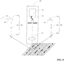
- FIG. 8 is a schematic view of a structure of a detection unit according to another embodiment of the present invention.
- the detection unit may include an optical detection system 801, a light source 802, a first light generation member 803 for generating first light, a second light generation member 804 for generating second light. These components will be described in detail below.
- Optical detection system 801 includes a lens 811 and a transducer 821 (e.g., a photodiode).
- Lens 811 is configured to converge light emitted from marks and direct the converged light to transducer 821.
- Transducer 821 is configured to receive the converged light and convert the received light into an electrical signal.
- Light source 802 is configured to generate a first light beam 812 and a second light beam 822.
- First light generation member 803 is disposed on one side of optical detection system 801 and includes a first mirror 813, a first lens 823, and a second mirror 833.
- First mirror 813 is configured to reflect first light beam 812.
- First lens 823 is configured to converge the reflected first light beam.
- Second mirror 833 is configured to reflect the converged first beam as a first incident light onto the marks at a first oblique angle.
- Second light generation member 804 is disposed on the other side of optical detection system 801 opposite first light generation member 803 and includes a third mirror 814, a second lens 824, and a fourth mirror 834.
- Third mirror 814 is configured to reflect second light beam 822.
- Second lens 824 is configured to converge the reflected second light beam.
- Fourth mirror 834 is configured to reflect the converged second beam as a second incident light onto the marks at a second oblique angle. In one embodiment, the first and second oblique angles have the same angle.
- the detection apparatus may further include a data acquisition module 831 for acquiring the electrical signal of transducer 821 and transmit the acquired electrical signal to a data processing device for further processing.
- the detection unit shown in FIG. 8 can be used for dark field detection. Under normal circumstances, when the incident light irradiates the marks at an oblique angle, the optical detection system cannot receive the reflected light or can only receive a small amount of light, the field of view is generally dark and is referred to as a dark field detection. And if the marks have defects, the incident light will be scattered, and the scattered light will be condensed by the lens. The transducer will pick up the condensed light, convert it to an electrical signal, and send the electrical signal to the image processing unit for further processing to detect defects of the marks. Further, the symmetrical positon of the first and second light beams with respect to the detection unit can reduce the adverse effects on the detection results caused by the lens distortion.
- the detection apparatus may be provided with the detection unit shown in FIG. 7 for detecting a defect-free mark. In some other embodiments, the detection apparatus may be provided with the detection unit shown in FIG. 8 for detecting a defective mark. In further embodiments, a portion of the detection device may be provided with the detection unit shown in FIG. 7 and another portion of the detection device may be provided with the detection unit shown in FIG. 8 so as to operate in a complementary manner.
- defects of a mark can be detected, and if the mark is defective, the desired information can still be obtained form the mark.
- Embodiments of the present invention also provide a detection device for detecting a mark on a substrate.
- the detection device may include any one of the above-described embodiments.
- the detection device may also include a substrate support platform for supporting a substrate. In one embodiment, the detection device may also include a vibration-proof platform for supporting a substrate and for detecting marks on the substrate.
- Embodiments of the present invention also provide a method for detecting a mark on a substrate.
- the method may be implemented using the above-described embodiments for detecting a mark on a substrate.
- the mark may include a plurality of first stripes (a first stripe group) and a plurality of second stripes (a second stripe group) that are arranged substantially parallel to each other and spaced apart from each other.
- the method may include the following steps:
- the detection unit it is possible to substantially align the detection unit with a corresponding mark that is to be detected by operating the positioning unit, thereby driving the detection module to move over the surface of the substrate to detect a corresponding mark.
- the method for detecting a mark according to embodiments of the present invention does not rely on an the optical imaging technique, so that there is no need to place the mark to the center of the field of view, there is no need for a fine adjustment operation, and there is no need to identify the optical image, thereby reducing the mark detection time.
- the method also eliminates the high precision alignment accuracy required in the prior art approaches. Thus, the mark detection cost is reduced, and the efficiency and throughput of the detection device are improved.
Landscapes
- Physics & Mathematics (AREA)
- General Physics & Mathematics (AREA)
- Length Measuring Devices By Optical Means (AREA)
- Exposure Of Semiconductors, Excluding Electron Or Ion Beam Exposure (AREA)
- Exposure And Positioning Against Photoresist Photosensitive Materials (AREA)
- Container, Conveyance, Adherence, Positioning, Of Wafer (AREA)
Abstract
Description
- This application claims priority to Chinese patent application No.
201610929499.3, filed on October 31, 2016 - The present invention relates generally to semiconductor technology. More particularly, embodiments of the present invention relate to an apparatus and method for detecting a mark on a substrate.
- Conventional overlay measurement devices rely on an optical imaging device to measure the relative positional deviation between two sets of marks. Since an optical imaging device usually has optical distortion, it is generally necessary to first move the marks to the center of the field of view of the optical imaging device and then detect the relative deviation between the positions of the two sets of marks using image recognition techniques, thereby eliminating the effect of optical distortion on the measurement results.
-
FIGS. 1A and 1B are plan views of a schematic representation of two sets of marks at the center of the field of view of an optical imaging device, as known in the art. As shown inFIGS. 1A and 1B , the position of amark 102A in the current layer in the X-direction and the position of anetched mark 102B in a previous layer in the Y-direction can be measured using image recognition techniques so that the relative deviation of the positions between the two sets of marks can be determined. - However, in the process of placing the marks to the center of the field of view of the optical imaging device, there may be an error due to the placement of the substrate on which the marks are disposed, therefore, it is generally necessary to fine tune the placement to place the marks to the center of the field of view, and the process is time consuming. Further, there is also a time required to identify the scanned image, so that it takes a relatively long time to measure a set of marks (e.g., 0.5-1 second).
- With ever decreasing size in technology nodes, the requirements for the set of measurements also increase and more sets of marks need to be measured. For example, if more than 60 exposure areas of a wafer are required to be measured, and assuming that each exposure area has five sets of marks, the measurement time will take about 5 minutes.
- Thus, there is a need for a novel measurement apparatus and method to reduce the measurement time of the marks.
- It is an object of the present invention to provide a method for detecting a mark on a substrate and an apparatus for detecting a plurality of marks on a substrate, which may reduce the measurement time of the marks, in particular which cost effectively and time efficiently enable detecting marks on a substrate.
- The object is achieved by the features of the respective independent claims. Further embodiments are defined in the respective dependent claims.
- A first aspect of the present invention provides an apparatus for detecting a plurality of marks on a substrate is provided. Each of the marks has a first stripe group and a second stripe group spaced apart from each other and disposed in parallel to each other. The apparatus includes at least one detection module moveable over a surface of the substrate along a first direction. The at least one detection module includes at least one detection unit configured to obtain data from a mark and operative to perform repeated acquisition operations on the first stripe group and the second stripe group of the mark, each of the acquisition operations is configured to acquire data associated with the first stripe group or the second stripe group of the mark, and at least one positioning unit configured to align the at least one detection unit with the mark in the first direction.
- Preferably, the first stripe group includes a plurality of first stripes, and the second stripe group includes a plurality of second stripes. The first and second stripes are spaced apart from each other and disposed in parallel to each other along the first direction. Preferably, the first stripes and the second stripes are alternately arranged with each other.
- Preferably, the apparatus further includes a data processing module configured to determine a positional deviation between the first and second stripe groups based on data obtained from the first and second stripe groups.
- Preferably, the obtained data includes a peak light intensity received from the first stripe group or from the second stripe group and a time associated with the received peak light intensity.
- Preferably, the plurality of marks include a plurality of columns of marks arranged along the first direction; the at least one detection unit includes a plurality of detection units; the at least one positioning unit includes a plurality of positioning units. Each of the positioning units is operative to align one of the detection units with a corresponding mark along the first direction.
- Preferably, the at least one detection module further includes a frame; the at least one positioning unit includes at least one support rod mounted to the frame and configured to support the at least one detection unit; and a positioning mechanism configured to move the at least one detection unit along the at least one support rod to a desired position to align the at least one detection unit with a mark.
- Preferably, the at least one support rod includes a screw bar, and the positioning mechanism moves the at least one detection unit along the screw bar. In one embodiment, the at least one detection unit includes a first hole and a second hole disposed vertically and a third hole disposed between the first and second holes, the third hole having internal threads, and the screw rod having external threads for engaging the internal threads of the third hole. The frame includes a first bracket and a second bracket disposed opposite to each other. The at least one support rod includes a first support rail passing through the first hole and a second support rail passing through the second hole and suspended between the first and second brackets. The screw rod passes through the third hole and drives the at least one detection unit along the first and second support rails when rotating.
- Preferably, the apparatus further includes an air cushion guide, and the air cushion guide includes a first rail extending in the first direction; a first slider engaged with the first rail and configured to support the first bracket; a second rail extending in the first direction; and a second slider engaged with the second rail and configured to support the second bracket. The first slider, when moving along the first rail, drives the first bracket along the first direction, and the second slider, when moving along the second rail, drives the second bracket along the first direction, so that the detection module moves above the surface of the substrate in the first direction.
- Preferably, the frame further includes a third bracket engaged with a first end of the first bracket and a first end of second bracket; and a fourth bracket opposite the third bracket and engaged with a second end of the first bracket and a second end of the second bracket.
- Preferably, the marks are disposed in a scribe line extending along the first direction. The marks are configured such that, when a placement error of the substrate is a first error, and a misalignment of the a center of a field of view of the at least one detection unit with respect to an ideal center axis of the scribe line is a second error, the at least one detection unit is configured to obtain the data from the marks disposed in the scribe line.
- Preferably, the at least one detection unit includes an optical image detection system. The optical image detection system includes a light source for generating light; a lens configured to converge the light generated by the light source to irradiate the marks; a semi-reflective mirror configured to reflect at least one portion of the light toward the lens to irradiate the marks and transmit at least one portion of the light emitted by the irradiated marks through the lens; and a transducer configured to receive the emitted portion of the light by the irradiated marks through the lens by the semi-reflective mirror and convert the received light into an electrical signal.
- Preferably, the at least one detection unit includes an optical image detection system, which includes a lens for converging light emitted from the marks; a transducer for receiving light from the lens and converting the received light into an electrical signal; and a light source for generating a first light beam and a second light beam. The optical image detection system also includes a first light generating member disposed on one side of the optical image detection system for generating a first light and having a first mirror for reflecting the first light beam; a first lens for converging the first light beam reflected by the first mirror to generate a converged first light beam; a second mirror for reflecting the converged first light beam to be incident onto the mark at a first oblique angle. The optical image detection system also includes a second light generating member disposed on one side of the optical detection image system for generating a first light and having a third mirror for reflecting the second light beam; a second lens for converging the second light beam reflected by the third mirror to generate a converged second light beam; and a fourth mirror for reflecting the converged second light beam to be incident onto the mark at a second oblique angle.
- Preferably, the at least one detection unit further includes a data acquisition module for acquiring the electrical signal of the transducer and sending the acquired electrical signal to a data processing device for processing.
- Preferably, the marks are etched marks, and the first stripe group includes marks of a current layer, and the second stripe group includes marks of a previous layer.
- Preferably, the at least one detection module uniformly accelerates or uniformly decelerates over the surface of the substrate in at least one direction.
- Preferably, the apparatus further includes a substrate support platform for supporting the substrate. In one embodiment, the apparatus also includes a vibration-proof platform for supporting the substrate support platform.
- A second aspect of the present invention provides a method for detecting a mark on a substrate. The mark includes a first stripe group and a second stripe group arranged in parallel to each other. The method includes providing a detection module having a detection unit and a positioning unit disposed over a surface of the substrate, the detection module configured to move over the surface of the substrate in a first direction to obtain data of the mark, aligning the detection unit with the mark by the positioning unit, and operating the detection module to detect the mark.
- The method according to the second aspect of the present invention may be carried out by an apparatus according to the first aspect of the present invention.
- The following description, together with the accompanying drawings, will provide a better understanding of the nature and advantages of the claimed invention.
- The accompanying drawings form a part of the present disclosure, that describe exemplary embodiments of the present invention. The drawings together with the specification will explain the principles of the invention.
-
FIGS. 1A and 1B are plan views of a schematic representation of two sets of marks at the center of the field of view of an optical imaging device, as known in the art; -
FIG. 2 is a perspective view illustrating a mark on a substrate according to one embodiment of the present disclosure; -
FIG. 3 is a perspective view illustrating a structure of an apparatus for detecting a mark on a substrate according to one embodiment of the present disclosure; -
FIG. 4 is a perspective view illustrating a structure of an apparatus for detecting a mark on a substrate according to another embodiment of the present disclosure; -
FIG. 5 is a perspective view illustrating a structure of a detection unit and a positioning unit according to one embodiment of the present disclosure; -
FIG. 6 is a plan view of a set of marks in a scribe line according to one embodiment of the present disclosure; -
FIG. 7 is a side view in partial cross section of a structure of an optical image detection device according to one embodiment of the present disclosure; and -
FIG. 8 is a side view in partial cross section of a structure of an optical image detection device according to another embodiment of the present disclosure. - In the following description, numerous specific details are provided for a thorough understanding of the present invention. However, it should be appreciated by those of skill in the art that the present invention may be realized without one or more of these details. In other examples, features and techniques known in the art will not be described for purposes of brevity.
- It will be understood that the drawings are not drawn to scale, and similar reference numbers are used for representing similar elements. Embodiments of the invention are described herein with reference to functional block diagrams that are schematic illustrations of idealized embodiments (and intermediate structures) of the invention.
- As used herein, the terms "a", "an" and "the" may include singular and plural references. It will be further understood that the terms "comprising", "including", having" and variants thereof, when used in this specification, specify the presence of stated features, steps, operations, elements, and/or components, but do not preclude the presence or addition of one or more other features, steps, operations, elements, components, and/or groups thereof. In contrast, the term "consisting of" when used in this specification, specifies the stated features, steps, operations, elements, and/or components, and precludes additional features, steps, operations, elements and/or components. Furthermore, as used herein, the words "and/or" may refer to and encompass any possible combinations of one or more of the associated listed items.
- It should be noted that the reference numerals and letters denoted similar items in the accompanying drawings, and therefor, once an item is defined in a drawing, its description will not be repeated in drawings that follow.
- Embodiments of the present disclosure provide a method for detecting marks without relying upon an optical imaging device that performs an imaging operation of the marls. In this way, the requirement on the lens is relatively low, and a conventional optical detection system can be used to detect the marks. The method according to embodiment of the present disclosure not only reduces the detection time of the marks, but also lowers the cost of test equipment (e.g., marking device).
-
FIG 2 is a perspective view of a mark on a substrate according to one embodiment of the present disclosure. As shown inFIG. 2 , the mark on the substrate may include a plurality of first stripes (first stripe group) 201 and a plurality of second stripes (second stripe group) 202 that are substantially parallel to each other and spaced apart from each other. In one embodiment,first stripes 201 may be the marking stripes of the current layer, andsecond stripes 202 may be the marking stripes of a previous layer. That is,first stripes 201 may be formed in a first layer, andsecond stripes 202 may be formed in a second layer that is different from the first layer. Thus, it is understood that, although the first and second stripes are shown to be substantially flush for the convenience of illustration inFIG. 2 , the first and second stripes can be disposed in different levels in certain embodiments. Illustratively,first stripes 201 andsecond stripes 202 may be a concave-convex pattern formed in corresponding layers. Further, in some embodiments, the first and second stripes may be configured to have different properties. In one example embodiment, the first and second stripes may be configured to have different surface reflectivity, such that one of the first and second stripes has a relatively smooth surface and the other one of the first and second stripes has a relatively rough surface. In another example embodiment, the first and second stripes may be configured to have different surface heights. It is to be understood that these are merely examples in order to better understand the various embodiments of the disclosure and are not intended to limit the invention, as long as the difference between the first and second stripes is distinguishable using any technical means (e.g., through information or data obtained from the stripes). In some other embodiments, each of the marks on the substrate may include a first group of stripes (a first stripe group) spaced apart from each other and a second group of stripes (a second stripe group) spaced apart from each other, as shown inFIG. 2 . Herein, the first group of stripes (the first stripe group) may include a plurality of first stripes adjacent to each other, and the second group of stripes (the second stripe group) may include a plurality of second stripes adjacent to each other. The first group of stripes and the second group of stripes are arranged parallel to each other along a certain direction. In one embodiment,first stripes 201 andsecond stripes 202 are disposed alternatively to each other, however, the present invention is not limited thereto. -
FIG. 3 is a perspective view illustrating an apparatus for detecting a mark on asubstrate 200 according to an embodiment of the present invention. For the sake of convenience of description, the term "an apparatus for detecting a mark on a substrate" is alternatively referred to as "a detection apparatus" or "a detection device" hereinafter. The mark on the surface ofsubstrate 200 may include the stripes described above. Referring toFIG. 3 , the detection apparatus (detection device) may include at least onedetection module 300.Detection module 300 is configured to be moveable over the surface ofsubstrate 200 along at least one direction (e.g., along the Y-direction). In some embodiments, the detection apparatus may include two detection modules, one of which is configured to be moveable over the surface ofsubstrate 200 along the X-direction, the other one is configured to be moveable over the surface ofsubstrate 200 along the Y-direction.Substrate 200 is shown as being supported by asubstrate support platform 203.Substrate support platform 203 may be any suitable platform for supporting or carrying a substrate known in the art or developed in the future. -
Detection module 300 may include at least onedetection unit 301 and at least onepositioning unit 302.Detection unit 301 is configured to obtain information (data) of a corresponding mark (e.g., as shown inFIG. 2 ). In the example embodiment shown inFIG. 3 , one or more marks may be located in atrack 204.Track 204 may be a scribe line of a semiconductor wafer, the mark may be an alignment mark imprinted on or etched into the scribe line.Track 204 is shown to be extending along the X-direction and/or the Y-direction. It should be understood thattrack 204 is merely an example, those of skill in the art will appreciate thattrack 204 may not be present or a virtual straight line. -
Detection unit 301 is configured to perform repeated acquisition operations on a first stripe group (i.e., first stripes 201) and a second stripe group (i.e., second stripes 202) of a corresponding mark. Each acquisition operation may obtain information (data) of the first stripe group or the second stripe group of the corresponding mark. In one embodiment, the obtained information (data) may include at least one of the peak light intensity received from the first stripe group or the second stripe group and the time at which the peak light intensity is received. -
Positioning unit 302 is configured to support and position a correspondingdetection unit 301.Positioning unit 302 is configured to operate such thatcorresponding detection unit 301 is substantially aligned with a corresponding mark in the X or Y direction of the detection module.Positioning unit 302 will be described in more detail later below. - According to the present invention, the detection unit may be substantially aligned with a corresponding mark to be detected by the positioning unit so that the detection module moves above the substrate using the detection unit for detecting the mark on the substrate. The method for detecting the mark does not depend from an optical imaging approach, and thus, there is no need to move the mark to the center of the field of view of the optical imaging lens and there is no need for a fine tuning operation, and there Is no need to identify the optical image, that reduces the detection time of the mark, and there is no need for a very precision alignment accuracy required in the prior art. Thus, the cost of mark detection is reduced, and the efficiency of the mark detection and the throughput of the detection apparatus are improved.
- Further, in some embodiments, the detection apparatus may also include a data processing module connected to the detection module using a wired or wireless communication connection to determine the positional deviation between the first stripe group and the second stripe group according to data obtained from the first stripe group and the second stripe group. The data processing module may be integrated in the detection apparatus (e.g., in the form of a processor) or it may be implemented as a separate component or device coupled to the detection apparatus using a wired or wireless communication link.
-
FIG. 4 is a perspective view illustrating a structure of an apparatus for detecting a mark on a substrate according to another embodiment of the present invention. In the embodiment,substrate 200 may include a plurality of columns of marks arranged along a certain position (e.g., the Y direction). Each column of marks may include a plurality of first stripes (first stripe group) 201 that are arranged in parallel and spaced apart from each other and a plurality of second stripes (second stripe group) 202 that are arranged in parallel and spaced apart from each other (as shown inFIG. 2 ).Detection module 300 may include a plurality ofdetection units 301 and a plurality ofpositioning units 302. Eachpositioning unit 302 is operative to align acorresponding detection unit 301 with a corresponding mark along the direction of the motion of the detection unit/module (e.g., in the Y direction as shown inFIG. 4 ). - In the embodiment, the detection unit may be aligned with a column of marks by the positioning unit so that
detection module 300 can detect multiple columns of marks when moving over the surface of the substrate along the Y direction to further reduce the detection time and improve the detection efficiency. - It is understood that, although three
detection units 301 and threepositioning units 302 are shown inFIG. 4 , this is merely illustrative and is not intended to limit the present invention. In practical applications, the number of detection units and positioning units can be determined according to actual requirements. - The detection apparatus may include a plurality of detection modules, for example, two detection modules. One of the detection modules is operative to detect one or more marks in a certain direction (e.g., the Y direction), and the another one of the detection modules is operative to detect one or more marks in another direction (e.g., the X direction). In the case where a plurality of columns of marks are arranged in both the X direction and the Y direction, one scanning operation in the X direction may detect all of the marks arranged in the X direction, and one scanning operation in the Y direction may detect all of the marks arranged in the Y direction. If the scanning speed is 1 m/s, the time to scan a 300 mm substrate is only slightly greater than 0.3 seconds. The time to completely scan the marks arranged in both X and Y directions is about 1 second, thus, the time of detecting all the marks of the substrate is greatly reduced.
- In one embodiment, referring to
FIG. 4 ,detection module 300 may also include a frame. The detection unit and the positioning unit may be directly or indirectly mounted on or supported by the frame. In one embodiment, the frame may include afirst bracket 303 and asecond bracket 304 disposed opposite to each other. In another embodiment, the frame may includefirst bracket 303,second bracket 304, athird bracket 305, and afourth bracket 306.Third bracket 305 andfourth bracket 306 are disposed opposite to each other and arranged in a certain direction (e.g., the Y direction).Third bracket 305 is engaged with a first end offirst bracket 303 and a first end ofsecond bracket 304, andfourth bracket 306 is engaged with a second end offirst bracket 303 and a second end ofsecond bracket 304. The first ends and the second ends of the first and second brackets are opposite to each other. The frame is configured to increase the weight of the detection device, thereby increasing the inertia of the detection device in motion, and to secure the positioning unit to a support rod (that will described in detail later below). - Referring still to
FIG. 4 , the detection device may also include anair cushion guide 400.Air cushion guide 400 may include afirst rail 401, afirst slider 402, asecond rail 403, and asecond slider 404.First rail 401 andsecond rail 402 extend in the same direction (e.g., the Y direction).First slider 402 is engaged with first rail 401 (e.g., disposed on first rail 401) to supportfirst bracket 303.Second slider 404 is engaged with second rail 403 (e.g., disposed on second rail 403) to supportsecond bracket 304.First slider 402 andsecond slider 404 are configured to slide alongfirst rail 401 andsecond rail 402. Whenfirst slider 402 andsecond slider 404 are driven to slide alongfirst rail 401 andsecond rail 402, they movefirst bracket 303 andsecond bracket 304 in a certain direction (e.g., the Y direction) so thatdetection module 300 can move over the surface ofsubstrate 200 in the certain direction and detect marks disposed in that direction. In one embodiment,detection module 300 is operative to move with a uniform acceleration and a uniform deceleration. -
FIG. 5 is a perspective view illustrating a structure of a detection unit and a positioning unit according to one embodiment of the present invention. Referring toFIG. 5 ,positioning unit 302 may include at least one support rod and apositioning mechanism 342. The support rod may be mounted or partially mounted on the frame (e.g., on the first bracket and/or the second bracket) and configured to support correspondingdetection unit 301.Positioning mechanism 342 is configured to drivedetection unit 301 along the support rod that secures the detection unit in a desired position so that the detection unit is aligned with a corresponding mark in a certain direction (e.g., the Y direction). In one embodiment, the support rod may include ascrew rod 312, andpositioning mechanism 342 may drivescrew rod 312 to position and aligndetection unit 301 with a mark. In one embodiment,positioning mechanism 342 may be a rotating motor that can drive the screw rod to properly positiondetection unit 301. - In practical applications, the detection unit and the positioning unit may be implemented using different approaches so that the positioning unit can cause the corresponding detection unit to be aligned with a corresponding mark in a certain direction (e.g., the Y direction).
- In one embodiment,
detection unit 301 may include afirst hole 3011 disposed in a first positon and asecond hole 3012 disposed in a second portion that is arranged vertically with respect to the first position, and athird hole 3013 disposed betweenfirst hole 3011 andsecond hole 3012. As shown inFIG. 5 ,third hole 3013 has an internal thread, and screwrod 312 has an external thread engaging the internal thread ofthird hole 3013. In the embodiment, the frame may includefirst bracket 303 andsecond bracket 304 opposite to each other (shown inFIG. 4 ). The support rod may includescrew rod 312, afirst support rail 322, asecond support rail 332, andpositioning mechanism 342.First support rail 322 andsecond support rail 332 pass through respectivefirst hole 3011 andsecond hole 3012 and suspended betweenfirst bracket 303 andsecond bracket 304. In one embodiment,first support 322 andsecond support rail 332 may be engaged withdetection unit 301 using a sliding bearing so thatdetection unit 301 can be moved along the support rail.Screw rod 312 passes throughthird hole 3013 so as to enabledetection unit 301 to move alongfirst support rail 322 andsecond support rail 332 when screw rod is rotated to causedetection unit 301 to align with a corresponding mark in a certain direction (e.g., the Y direction). -
FIG. 6 is a plan view of one ormore marks 601 in a scribe line according to one embodiment of the present invention. Referring toFIG. 6 , one ormore marks 601 may be provided on a substrate such as in ascribe line 602 in the Y direction.Scribe line 602 may extend along the X direction and/or the Y direction.Marks 601 may be any of the above-described marks, e.g., each of the marks may include the first stripe group having a plurality of first stripes and the second stripe group having a plurality of second stripes, as shown inFIG. 2 . In the embodiment, marks 601 may be configured such that, when an error on the substrate is a first error, and a misalignment error of the center of the field of view of the detection unit with respect to the ideal center axis ofscribe line 602 is a second error, the detection unit can be configured to obtain data from the marks disposed in the scribe line. It is appreciated that, marks 601 may include a plurality of marks disposed in the Y direction or in the X direction, and each of the marks may include the first stripe group and a second stripe group. - In one exemplary embodiment, the scribe line has a width of 70 µm, the substrate placement error is 15 µm, the adjustment accuracy of the screw rod is 10 µm, the width of the field of view is 20 µm, the width of the mark may be set to the range between 40 µm and 70 µm. In this way, when the detection apparatus is operative to detect the mark, only the detection unit is positioned within the adjustment accuracy error, and all the marks in the corresponding scribe lines can be detected in one scanning operation. Thus, it is only necessary to perform a relatively coarse alignment to perform efficient measurements without the need for precise alignment as required in the prior art approach, thereby greatly reducing the mark detection time, improving the detection efficiency and reducing the equipment accuracy requirements to reduce the equipment cost.
- With regard to the marks, some of the marks may have defects, e.g., undesirable particles or dust are present on the surface of the marks. In practical applications, the detection apparatus may be equipped with different types of detection units to detect defects of the marks or to prevent adverse effects of the mark defects on the detection. As an example, two structures of the detection unit will be described below.
-
FIG. 7 is a schematic view of a structure of a detection unit according to one embodiment of the present invention. Referring toFIG. 7 , the detection unit may include anoptical detection system 700. In one embodiment,optical detection system 700 may include alight source 701, anoptional mirror 702, a semi-transparent and semi-reflective mirror (alternatively referred to as beam splitter or semi-reflective mirror hereinafter) 703, alens 704, and a transducer (e.g., a photodiode).Light source 701 may be, for example, a light emitting diode for generating light.Optional mirror 702 is configured to reflect light generated bylight source 701. Semi-reflective mirror (beam splitter) 703 is configured to reflect at least one portion of light (e.g., light reflected by mirror 702) generated bylight source 701 towardlens 704 to irradiate a mark on the substrate (shown as first andsecond stripes 201 and 202) and at least one portion of light emitted by the irradiated mark throughlens 704.Lens 704 is configured to converge light fromsemi-reflective mirror 703 toward the irradiated mark and converge light emitted from the marks towardsemi-reflective mirror 703 as an optical signal.Transducer 705 is configured to receive the optical signal throughsemi-reflective mirror 703 and convert the received optical signal into an electrical signal. - In one embodiment, the detection apparatus may further include a
data acquisition module 706 coupled totransducer 705 and configured to acquire or obtain the electrical signal of the transducer and provide the acquired or obtained electrical signal to a processing device for processing. - The detection unit shown in
FIG. 7 may be used to irradiate the detection field with light (illuminating the detection field), and the detection unit can be moved along the horizontal direction indicated an arrow (horizontal arrow facing to the right). In general, for illuminating the detection field, light reflected of the surface of the irradiated mark back to the optical detection system has a relatively high light intensity, so that the field of view is generally is well illuminated. The illuminated detection field can recognize marks based on the reflected light received from the surface of the mark. For marks that have no defects, light incident vertically to the marks will be substantially (or the majority of it) reflected back toward transducer (e.g., photodiode) 705, so that the detection unit can detect the marks based on the reflected light. - If the marks have defects, light incident onto the marks will be scattered, and the light intensity of the reflected light from the marks is relatively weak, so that defects of the marks can be detected. However, in this case, the presence of defects in the marks will affect, for example, the identification of the pitch between the stripes.
- To overcome this problem, embodiments of the present invention also provide another detection unit.
FIG. 8 is a schematic view of a structure of a detection unit according to another embodiment of the present invention. Referring toFIG. 8 , the detection unit may include anoptical detection system 801, alight source 802, a firstlight generation member 803 for generating first light, a secondlight generation member 804 for generating second light. These components will be described in detail below. -
Optical detection system 801 includes alens 811 and a transducer 821 (e.g., a photodiode).Lens 811 is configured to converge light emitted from marks and direct the converged light totransducer 821.Transducer 821 is configured to receive the converged light and convert the received light into an electrical signal. -
Light source 802 is configured to generate afirst light beam 812 and a secondlight beam 822. - First
light generation member 803 is disposed on one side ofoptical detection system 801 and includes afirst mirror 813, afirst lens 823, and asecond mirror 833.First mirror 813 is configured to reflectfirst light beam 812.First lens 823 is configured to converge the reflected first light beam.Second mirror 833 is configured to reflect the converged first beam as a first incident light onto the marks at a first oblique angle. - Second
light generation member 804 is disposed on the other side ofoptical detection system 801 opposite firstlight generation member 803 and includes athird mirror 814, asecond lens 824, and afourth mirror 834.Third mirror 814 is configured to reflect secondlight beam 822.Second lens 824 is configured to converge the reflected second light beam.Fourth mirror 834 is configured to reflect the converged second beam as a second incident light onto the marks at a second oblique angle. In one embodiment, the first and second oblique angles have the same angle. - In one embodiment, the detection apparatus may further include a
data acquisition module 831 for acquiring the electrical signal oftransducer 821 and transmit the acquired electrical signal to a data processing device for further processing. - The detection unit shown in
FIG. 8 can be used for dark field detection. Under normal circumstances, when the incident light irradiates the marks at an oblique angle, the optical detection system cannot receive the reflected light or can only receive a small amount of light, the field of view is generally dark and is referred to as a dark field detection. And if the marks have defects, the incident light will be scattered, and the scattered light will be condensed by the lens. The transducer will pick up the condensed light, convert it to an electrical signal, and send the electrical signal to the image processing unit for further processing to detect defects of the marks. Further, the symmetrical positon of the first and second light beams with respect to the detection unit can reduce the adverse effects on the detection results caused by the lens distortion. - In some embodiments, the detection apparatus may be provided with the detection unit shown in
FIG. 7 for detecting a defect-free mark. In some other embodiments, the detection apparatus may be provided with the detection unit shown inFIG. 8 for detecting a defective mark. In further embodiments, a portion of the detection device may be provided with the detection unit shown inFIG. 7 and another portion of the detection device may be provided with the detection unit shown inFIG. 8 so as to operate in a complementary manner. - Thus, according to embodiments of the present invention, defects of a mark can be detected, and if the mark is defective, the desired information can still be obtained form the mark.
- Embodiments of the present invention also provide a detection device for detecting a mark on a substrate. The detection device may include any one of the above-described embodiments.
- In one embodiment, the detection device may also include a substrate support platform for supporting a substrate. In one embodiment, the detection device may also include a vibration-proof platform for supporting a substrate and for detecting marks on the substrate.
- Embodiments of the present invention also provide a method for detecting a mark on a substrate. The method may be implemented using the above-described embodiments for detecting a mark on a substrate. The mark may include a plurality of first stripes (a first stripe group) and a plurality of second stripes (a second stripe group) that are arranged substantially parallel to each other and spaced apart from each other. The method may include the following steps:
- Step S 1: providing a substrate, which can be a silicon wafer having the above-described mark.
- Step S2: providing a detection module. The detection module can be moved over a surface of the substrate along at least one direction (e.g., along the above-described X or Y direction). The detection module includes at least one detection unit and at least one positioning unit. The detection unit is configured to obtain information from a corresponding mark; the detection unit is also configured to be able to perform a repeated acquisition operation to obtain information from the first stripes and from the second stripes, respectively. Each acquisition operation obtains information from the first stripes or from the second stripes in the corresponding mark. The positioning unit is configured to support and position a corresponding detection unit.
- Step S3: operating the positioning unit to align the detection unit with a corresponding mark along a certain direction (e.g., along the Y direction).
- Step S4: driving the detection module in the certain direction to detect the mark.
- In the embodiment, it is possible to substantially align the detection unit with a corresponding mark that is to be detected by operating the positioning unit, thereby driving the detection module to move over the surface of the substrate to detect a corresponding mark. The method for detecting a mark according to embodiments of the present invention does not rely on an the optical imaging technique, so that there is no need to place the mark to the center of the field of view, there is no need for a fine adjustment operation, and there is no need to identify the optical image, thereby reducing the mark detection time. The method also eliminates the high precision alignment accuracy required in the prior art approaches. Thus, the mark detection cost is reduced, and the efficiency and throughput of the detection device are improved.
- While the present invention is described herein with reference to illustrative embodiments, this description is not intended to be construed in a limiting sense. Rather, the purpose of the illustrative embodiments is to make present invention be better understood by those skilled in the art. In order not to obscure the invention, many details of well-known processes and manufacturing techniques are omitted.
- Furthermore, some of the features of the preferred embodiments of the present invention could be used to advantage without the corresponding use of other features. As such, the foregoing description should be considered as merely illustrative of the principles of the invention, and not in limitation thereof.
Claims (15)
- An apparatus for detecting a plurality of marks on a substrate, each of the marks having a first stripe group and a second stripe group spaced apart from each other and disposed in parallel to each other, the apparatus comprising:at least one detection module moveable over a surface of the substrate along a first direction, the at least one detection module comprising:at least one detection unit configured to obtain data from a mark and operable to perform repeated acquisition operations on the first stripe group and the second stripe group of the mark, each of the acquisition operations acquiring data associated with the first stripe group or the second stripe group of the mark; andat least one positioning unit configured to align the at least one detection unit with the mark in the first direction.
- The apparatus of claim 1, wherein the first stripe group comprises a plurality of first stripes, and the second stripe group comprises a plurality of second stripes, the first and second stripes are spaced apart from each other and disposed in parallel to each other along the first direction;
wherein preferably: the first stripes and the second stripes are alternately arranged with each other. - The apparatus of claim 1 or 2, further comprising:a data processing module configured to determine a positional deviation between the first and second stripe groups based on the data obtained from the first and second stripe groups.
- The apparatus of anyone of the claims 1-3, wherein the obtained data comprises a peak light intensity received from the first stripe group or from the second stripe group and a time associated with the received peak light intensity.
- The apparatus of anyone of the claims 1-4, wherein the at least one detection module further comprises a frame;
the at least one positioning unit comprises:at least one support rod mounted to the frame and configured to support the at least one detection unit; anda positioning mechanism configured to move the at least one detection unit along the at least one support rod to a desired position to align the at least one detection unit with a mark. - The apparatus of claim 5, wherein the at least one support rod comprises a screw rod, and the positioning mechanism drives the at least one detection unit using the screw rod.
- The apparatus of claim 6, wherein the at least one detection unit comprises first and second holes arranged vertically with respect to each other and a third hole disposed between the first and second holes, the third hole having an internal thread, and the screw rod having an external thread engaging the internal thread of the third hole;
the frame comprises a first bracket and a second bracket disposed opposite to each other;
the at least one support rod comprises a first support rail passing through the first hole and a second support rail passing through the second hole and suspended between the first and second brackets;
the screw rod passing through the third hole drives the at least one detection unit along the first and second support rails when rotating. - The apparatus of claim 7, further comprising an air cushion guide, the air cushion guide comprising:a first rail extending in the first direction;a first slider engaged with the first rail and configured to support the first bracket;a second rail extending in the first direction; anda second slider engaged with the second rail and configured to support the second bracket,the first slider when moving along the first rail drives the first bracket along the first direction and the second slider when moving along the second rail drives the second bracket along the first direction, so that the detection module moves above the surface of the substrate in the first direction.
- The apparatus of claim 7 or 8, wherein the frame further comprises:a third bracket engaged with a first end of the first bracket and a first end of second bracket; anda fourth bracket opposite the third bracket and engaged with a second end of the first bracket and a second end of the second bracket.
- The apparatus of anyone of the claims 1-9, wherein the at least one detection unit comprises an optical image detection system, the optical image detection system comprising:a light source for generating light;a lens configured to converge the light generated by the light source to irradiate the marks;a semi-reflective mirror configured to reflect at least one portion of the light toward the lens to irradiate the marks and transmit at least one portion of the light emitted by the irradiated marks through the lens; anda transducer configured to receive the emitted portion of the light by the irradiated marks through the lens by the semi-reflective mirror and convert the received light into an electrical signal.
- The apparatus of anyone of the claims 1-10, wherein the at least one detection unit comprises a optical image detection system, the optical image detection system comprising:a lens for converging light emitted from the marks;a transducer for receiving light from the lens and converting the received light into an electrical signal;a light source for generating a first light beam and a second light beam;a first light generating member disposed on one side of the optical image detection system for generating a first light and comprising:a first mirror for reflecting the first light beam;a first lens for converging the first light beam reflected by the first mirror to generate a converged first light beam;a second mirror for reflecting the converged first light beam to be incident onto the mark at a first oblique angle;a second light generating member disposed on one side of the optical detection image system for generating a first light and comprising:a third mirror for reflecting the second light beam;a second lens for converging the second light beam reflected by the third mirror to generate a converged second light beam; anda fourth mirror for reflecting the converged second light beam to be incident onto the mark at a second oblique angle; andwherein, preferably, the at least one detection unit further comprises: a data acquisition module for acquiring the electrical signal of the transducer and providing the acquired electrical signal to a data processing device for processing.
- The apparatus of anyone of the claims 1-11, wherein at least one of:- the marks are marks etched into the substrate, and the first stripe group comprises etched marks of a current layer, and the second stripe group comprises etched marks of a previous layer;- the marks are disposed in a scribe line extending along the first direction, and the marks are configured such that, when a placement error of the substrate is a first error, and a misalignment of the a center of a field of view of the at least one detection unit with respect to an ideal center axis of the scribe line is a second error, the at least one detection unit is configured to obtain data from the marks disposed in the scribe line; and- the plurality of marks comprise a plurality of columns of marks arranged along the first direction, the at least one detection unit comprising a plurality of detection units, and the at least one positioning unit comprising a plurality of positioning units, each of the positioning units operative to align one of the detection units with a corresponding mark arranged along the first direction.
- The apparatus of anyone of the claims 1-12, wherein the at least one detection module uniformly accelerates or uniformly decelerates over the surface of the substrate along the first direction.
- The apparatus of anyone of the claims 1-13, further comprising a substrate support platform for supporting the substrate; and
wherein, preferably, the apparatus further comprises a vibration-proof platform for supporting the substrate support platform. - A method for detecting a mark on a substrate, the mark comprising a first stripe group and a second stripe group arranged in parallel to each other, the method comprising:providing a detection module having a detection unit and a positioning unit disposed over a surface of the substrate, the detection module configured to move over the surface of the substrate in a first direction to obtain data of the mark;aligning the detection unit with the mark by the positioning unit; andoperating the detection module to detect the mark.
Applications Claiming Priority (1)
| Application Number | Priority Date | Filing Date | Title |
|---|---|---|---|
| CN201610929499.3A CN108010855B (en) | 2016-10-31 | 2016-10-31 | Apparatus, apparatus and method for detecting marks on substrates |
Publications (2)
| Publication Number | Publication Date |
|---|---|
| EP3316038A2 true EP3316038A2 (en) | 2018-05-02 |
| EP3316038A3 EP3316038A3 (en) | 2018-06-27 |
Family
ID=60201851
Family Applications (1)
| Application Number | Title | Priority Date | Filing Date |
|---|---|---|---|
| EP17198880.1A Withdrawn EP3316038A3 (en) | 2016-10-31 | 2017-10-27 | Apparatus and method for detecting overlay mark with bright and dark fields |
Country Status (3)
| Country | Link |
|---|---|
| US (1) | US10658210B2 (en) |
| EP (1) | EP3316038A3 (en) |
| CN (1) | CN108010855B (en) |
Families Citing this family (7)
| Publication number | Priority date | Publication date | Assignee | Title |
|---|---|---|---|---|
| CN108022847B (en) * | 2016-10-31 | 2020-12-18 | 中芯国际集成电路制造(上海)有限公司 | Apparatus, apparatus and method for detecting marks on substrates |
| WO2022040221A1 (en) | 2020-08-17 | 2022-02-24 | Tokyo Electron Limited | Method for producing overlay results with absolute reference for semiconductor manufacturing |
| US11899375B2 (en) * | 2020-11-20 | 2024-02-13 | Kla Corporation | Massive overlay metrology sampling with multiple measurement columns |
| TWI776339B (en) * | 2020-12-30 | 2022-09-01 | 致茂電子股份有限公司 | Optical inspection equipment in semiconductor process system |
| US11719533B2 (en) * | 2021-03-28 | 2023-08-08 | Kla Corporation | Modulation of scanning velocity during overlay metrology |
| CN115616862B (en) * | 2021-07-15 | 2026-04-24 | 长鑫存储技术有限公司 | Measurement markers, semiconductor structures, measurement methods, equipment, and storage media |
| US20250271775A1 (en) * | 2024-02-22 | 2025-08-28 | Kla Corporation | Off-axis through the lens mutually coherent dark field imaging system with incoherent light for overlay metrology |
Family Cites Families (15)
| Publication number | Priority date | Publication date | Assignee | Title |
|---|---|---|---|---|
| US4907157A (en) * | 1984-09-05 | 1990-03-06 | Kabushiki Kaisha Toshiba | Method and system for allowing imaging of any size object through use of separate source and detector unit |
| US4710026A (en) * | 1985-03-22 | 1987-12-01 | Nippon Kogaku K. K. | Position detection apparatus |
| JP3352249B2 (en) * | 1993-10-26 | 2002-12-03 | キヤノン株式会社 | Position shift detector |
| JPH08233555A (en) * | 1994-12-28 | 1996-09-13 | Matsushita Electric Ind Co Ltd | Resist pattern measuring method and resist pattern measuring apparatus |
| US6023338A (en) * | 1996-07-12 | 2000-02-08 | Bareket; Noah | Overlay alignment measurement of wafers |
| JP3907497B2 (en) * | 2002-03-01 | 2007-04-18 | キヤノン株式会社 | POSITIONING APPARATUS, CONTROL METHOD THEREFOR, EXPOSURE APPARATUS, AND MANUFACTURING METHOD FOR MANUFACTURING SEMICONDUCTOR DEVICE BY EXPOSURE APPARATUS CONTROLLED BY THE CONTROL METHOD |
| US6921946B2 (en) * | 2002-12-16 | 2005-07-26 | Koninklijke Philips Electronics N.V. | Test structure for electrical well-to-well overlay |
| US6967709B2 (en) * | 2003-11-26 | 2005-11-22 | International Business Machines Corporation | Overlay and CD process window structure |
| NL2006228A (en) * | 2010-03-17 | 2011-09-20 | Asml Netherlands Bv | Alignment mark, substrate, set of patterning devices, and device manufacturing method. |
| EP2458441B1 (en) * | 2010-11-30 | 2022-01-19 | ASML Netherlands BV | Measuring method, apparatus and substrate |
| CN103777467B (en) * | 2012-10-19 | 2016-07-06 | 上海微电子装备有限公司 | A kind of overlay error measurement apparatus and method |
| CN103969960B (en) * | 2013-02-04 | 2016-07-06 | 上海微电子装备有限公司 | The apparatus and method that a kind of alignment is measured |
| US20150184729A1 (en) * | 2014-01-02 | 2015-07-02 | National Chung Cheng University | Ball screw capable of sensing push force in real time |
| CN104716070B (en) * | 2015-04-03 | 2017-12-26 | 合肥京东方光电科技有限公司 | Size detecting device and substrate loading device |
| WO2017050503A1 (en) * | 2015-09-22 | 2017-03-30 | Asml Netherlands B.V. | A method and apparatus for determining at least one property of patterning device marker features |
-
2016
- 2016-10-31 CN CN201610929499.3A patent/CN108010855B/en active Active
-
2017
- 2017-10-27 EP EP17198880.1A patent/EP3316038A3/en not_active Withdrawn
- 2017-10-30 US US15/797,891 patent/US10658210B2/en active Active
Non-Patent Citations (1)
| Title |
|---|
| None |
Also Published As
| Publication number | Publication date |
|---|---|
| CN108010855A (en) | 2018-05-08 |
| EP3316038A3 (en) | 2018-06-27 |
| US20180122668A1 (en) | 2018-05-03 |
| US10658210B2 (en) | 2020-05-19 |
| CN108010855B (en) | 2020-04-14 |
Similar Documents
| Publication | Publication Date | Title |
|---|---|---|
| US10658210B2 (en) | Apparatus and method for detecting overlay mark with bright and dark fields | |
| US10553470B2 (en) | Wafer alignment method and apparatus for overlay measurement | |
| CN101546134A (en) | Electron beam writing apparatus and electron beam writing method | |
| JP2523227Y2 (en) | Foreign matter inspection device | |
| US8614798B2 (en) | Pattern generators, calibration systems and methods for patterning workpieces | |
| US10679881B2 (en) | Overlay measurement method and apparatus | |
| KR101232582B1 (en) | Laser processing method, laser processing apparatus and method of manufacturing a solar panel | |
| KR101917131B1 (en) | Optical inspecting apparatus | |
| JPH0534124A (en) | Foreign-matter inspecting apparatus | |
| WO2008149372A2 (en) | Apparatus and method for substrate handling | |
| US6744512B2 (en) | Position measuring apparatus and exposure apparatus | |
| CN108701679B (en) | Marking position correction device and method | |
| KR101823101B1 (en) | Optical inspecting apparatus | |
| JP6684992B2 (en) | Projection inspection device and bump inspection device | |
| JP2011177770A (en) | Laser beam working system and method for manufacturing solar panel | |
| JP2011177771A (en) | Laser beam machining method, laser beam machining apparatus, and method for manufacturing solar panel | |
| CN113866587B (en) | A flying probe test equipment | |
| WO2024022006A1 (en) | Calibration system, measurement and calibration tool, and calibration method | |
| KR20140123860A (en) | Thin film deposition apparatus and method for forming thin film using the same | |
| CN220525679U (en) | Detection equipment and focus detection device | |
| US8098382B2 (en) | Beam scanner and surface measurement apparatus | |
| WO2025153854A1 (en) | Multi purpose channel for optical metrology | |
| WO2026042357A1 (en) | Drawing device, correction information generation device, drawing method, and correction information generation method | |
| JP2007299805A (en) | Calibration method of gap detection value | |
| JP2000055927A (en) | Scanning probe microscope |
Legal Events
| Date | Code | Title | Description |
|---|---|---|---|
| PUAI | Public reference made under article 153(3) epc to a published international application that has entered the european phase |
Free format text: ORIGINAL CODE: 0009012 |
|
| STAA | Information on the status of an ep patent application or granted ep patent |
Free format text: STATUS: THE APPLICATION HAS BEEN PUBLISHED |
|
| AK | Designated contracting states |
Kind code of ref document: A2 Designated state(s): AL AT BE BG CH CY CZ DE DK EE ES FI FR GB GR HR HU IE IS IT LI LT LU LV MC MK MT NL NO PL PT RO RS SE SI SK SM TR |
|
| AX | Request for extension of the european patent |
Extension state: BA ME |
|
| PUAL | Search report despatched |
Free format text: ORIGINAL CODE: 0009013 |
|
| AK | Designated contracting states |
Kind code of ref document: A3 Designated state(s): AL AT BE BG CH CY CZ DE DK EE ES FI FR GB GR HR HU IE IS IT LI LT LU LV MC MK MT NL NO PL PT RO RS SE SI SK SM TR |
|
| AX | Request for extension of the european patent |
Extension state: BA ME |
|
| RIC1 | Information provided on ipc code assigned before grant |
Ipc: G03F 7/20 20060101AFI20180523BHEP |
|
| RAP1 | Party data changed (applicant data changed or rights of an application transferred) |
Owner name: SEMICONDUCTOR MANUFACTURING INTERNATIONAL (BEIJING Owner name: SEMICONDUCTOR MANUFACTURING INTERNATIONAL (SHANGHA |
|
| STAA | Information on the status of an ep patent application or granted ep patent |
Free format text: STATUS: REQUEST FOR EXAMINATION WAS MADE |
|
| 17P | Request for examination filed |
Effective date: 20181220 |
|
| RBV | Designated contracting states (corrected) |
Designated state(s): AL AT BE BG CH CY CZ DE DK EE ES FI FR GB GR HR HU IE IS IT LI LT LU LV MC MK MT NL NO PL PT RO RS SE SI SK SM TR |
|
| STAA | Information on the status of an ep patent application or granted ep patent |
Free format text: STATUS: EXAMINATION IS IN PROGRESS |
|
| 17Q | First examination report despatched |
Effective date: 20211028 |
|
| STAA | Information on the status of an ep patent application or granted ep patent |
Free format text: STATUS: THE APPLICATION IS DEEMED TO BE WITHDRAWN |
|
| 18D | Application deemed to be withdrawn |
Effective date: 20220308 |