EP3316025A1 - Display device and multi-display device - Google Patents
Display device and multi-display device Download PDFInfo
- Publication number
- EP3316025A1 EP3316025A1 EP16206939.7A EP16206939A EP3316025A1 EP 3316025 A1 EP3316025 A1 EP 3316025A1 EP 16206939 A EP16206939 A EP 16206939A EP 3316025 A1 EP3316025 A1 EP 3316025A1
- Authority
- EP
- European Patent Office
- Prior art keywords
- pixels
- substrate
- triangular
- display device
- triangular substrate
- Prior art date
- Legal status (The legal status is an assumption and is not a legal conclusion. Google has not performed a legal analysis and makes no representation as to the accuracy of the status listed.)
- Withdrawn
Links
Images









Classifications
-
- G—PHYSICS
- G06—COMPUTING OR CALCULATING; COUNTING
- G06F—ELECTRIC DIGITAL DATA PROCESSING
- G06F3/00—Input arrangements for transferring data to be processed into a form capable of being handled by the computer; Output arrangements for transferring data from processing unit to output unit, e.g. interface arrangements
- G06F3/14—Digital output to display device ; Cooperation and interconnection of the display device with other functional units
- G06F3/1423—Digital output to display device ; Cooperation and interconnection of the display device with other functional units controlling a plurality of local displays, e.g. CRT and flat panel display
- G06F3/1446—Digital output to display device ; Cooperation and interconnection of the display device with other functional units controlling a plurality of local displays, e.g. CRT and flat panel display display composed of modules, e.g. video walls
-
- G—PHYSICS
- G09—EDUCATION; CRYPTOGRAPHY; DISPLAY; ADVERTISING; SEALS
- G09F—DISPLAYING; ADVERTISING; SIGNS; LABELS OR NAME-PLATES; SEALS
- G09F9/00—Indicating arrangements for variable information in which the information is built-up on a support by selection or combination of individual elements
- G09F9/30—Indicating arrangements for variable information in which the information is built-up on a support by selection or combination of individual elements in which the desired character or characters are formed by combining individual elements
- G09F9/302—Indicating arrangements for variable information in which the information is built-up on a support by selection or combination of individual elements in which the desired character or characters are formed by combining individual elements characterised by the form or geometrical disposition of the individual elements
- G09F9/3023—Segmented electronic displays
-
- G—PHYSICS
- G09—EDUCATION; CRYPTOGRAPHY; DISPLAY; ADVERTISING; SEALS
- G09F—DISPLAYING; ADVERTISING; SIGNS; LABELS OR NAME-PLATES; SEALS
- G09F9/00—Indicating arrangements for variable information in which the information is built-up on a support by selection or combination of individual elements
- G09F9/30—Indicating arrangements for variable information in which the information is built-up on a support by selection or combination of individual elements in which the desired character or characters are formed by combining individual elements
- G09F9/302—Indicating arrangements for variable information in which the information is built-up on a support by selection or combination of individual elements in which the desired character or characters are formed by combining individual elements characterised by the form or geometrical disposition of the individual elements
- G09F9/3026—Video wall, i.e. stackable semiconductor matrix display modules
-
- G—PHYSICS
- G02—OPTICS
- G02F—OPTICAL DEVICES OR ARRANGEMENTS FOR THE CONTROL OF LIGHT BY MODIFICATION OF THE OPTICAL PROPERTIES OF THE MEDIA OF THE ELEMENTS INVOLVED THEREIN; NON-LINEAR OPTICS; FREQUENCY-CHANGING OF LIGHT; OPTICAL LOGIC ELEMENTS; OPTICAL ANALOGUE/DIGITAL CONVERTERS
- G02F1/00—Devices or arrangements for the control of the intensity, colour, phase, polarisation or direction of light arriving from an independent light source, e.g. switching, gating or modulating; Non-linear optics
- G02F1/01—Devices or arrangements for the control of the intensity, colour, phase, polarisation or direction of light arriving from an independent light source, e.g. switching, gating or modulating; Non-linear optics for the control of the intensity, phase, polarisation or colour
- G02F1/13—Devices or arrangements for the control of the intensity, colour, phase, polarisation or direction of light arriving from an independent light source, e.g. switching, gating or modulating; Non-linear optics for the control of the intensity, phase, polarisation or colour based on liquid crystals, e.g. single liquid crystal display cells
- G02F1/133—Constructional arrangements; Operation of liquid crystal cells; Circuit arrangements
- G02F1/1333—Constructional arrangements; Manufacturing methods
- G02F1/1335—Structural association of cells with optical devices, e.g. polarisers or reflectors
- G02F1/133509—Filters, e.g. light shielding masks
- G02F1/133512—Light shielding layers, e.g. black matrix
-
- G—PHYSICS
- G02—OPTICS
- G02F—OPTICAL DEVICES OR ARRANGEMENTS FOR THE CONTROL OF LIGHT BY MODIFICATION OF THE OPTICAL PROPERTIES OF THE MEDIA OF THE ELEMENTS INVOLVED THEREIN; NON-LINEAR OPTICS; FREQUENCY-CHANGING OF LIGHT; OPTICAL LOGIC ELEMENTS; OPTICAL ANALOGUE/DIGITAL CONVERTERS
- G02F1/00—Devices or arrangements for the control of the intensity, colour, phase, polarisation or direction of light arriving from an independent light source, e.g. switching, gating or modulating; Non-linear optics
- G02F1/01—Devices or arrangements for the control of the intensity, colour, phase, polarisation or direction of light arriving from an independent light source, e.g. switching, gating or modulating; Non-linear optics for the control of the intensity, phase, polarisation or colour
- G02F1/13—Devices or arrangements for the control of the intensity, colour, phase, polarisation or direction of light arriving from an independent light source, e.g. switching, gating or modulating; Non-linear optics for the control of the intensity, phase, polarisation or colour based on liquid crystals, e.g. single liquid crystal display cells
- G02F1/133—Constructional arrangements; Operation of liquid crystal cells; Circuit arrangements
- G02F1/1333—Constructional arrangements; Manufacturing methods
- G02F1/1343—Electrodes
- G02F1/134309—Electrodes characterised by their geometrical arrangement
-
- G—PHYSICS
- G06—COMPUTING OR CALCULATING; COUNTING
- G06F—ELECTRIC DIGITAL DATA PROCESSING
- G06F3/00—Input arrangements for transferring data to be processed into a form capable of being handled by the computer; Output arrangements for transferring data from processing unit to output unit, e.g. interface arrangements
- G06F3/14—Digital output to display device ; Cooperation and interconnection of the display device with other functional units
- G06F3/1423—Digital output to display device ; Cooperation and interconnection of the display device with other functional units controlling a plurality of local displays, e.g. CRT and flat panel display
-
- G—PHYSICS
- G09—EDUCATION; CRYPTOGRAPHY; DISPLAY; ADVERTISING; SEALS
- G09G—ARRANGEMENTS OR CIRCUITS FOR CONTROL OF INDICATING DEVICES USING STATIC MEANS TO PRESENT VARIABLE INFORMATION
- G09G3/00—Control arrangements or circuits, of interest only in connection with visual indicators other than cathode-ray tubes
- G09G3/001—Control arrangements or circuits, of interest only in connection with visual indicators other than cathode-ray tubes using specific devices not provided for in groups G09G3/02 - G09G3/36, e.g. using an intermediate record carrier such as a film slide; Projection systems; Display of non-alphanumerical information, solely or in combination with alphanumerical information, e.g. digital display on projected diapositive as background
- G09G3/003—Control arrangements or circuits, of interest only in connection with visual indicators other than cathode-ray tubes using specific devices not provided for in groups G09G3/02 - G09G3/36, e.g. using an intermediate record carrier such as a film slide; Projection systems; Display of non-alphanumerical information, solely or in combination with alphanumerical information, e.g. digital display on projected diapositive as background to produce spatial visual effects
-
- G—PHYSICS
- G09—EDUCATION; CRYPTOGRAPHY; DISPLAY; ADVERTISING; SEALS
- G09G—ARRANGEMENTS OR CIRCUITS FOR CONTROL OF INDICATING DEVICES USING STATIC MEANS TO PRESENT VARIABLE INFORMATION
- G09G3/00—Control arrangements or circuits, of interest only in connection with visual indicators other than cathode-ray tubes
- G09G3/20—Control arrangements or circuits, of interest only in connection with visual indicators other than cathode-ray tubes for presentation of an assembly of a number of characters, e.g. a page, by composing the assembly by combination of individual elements arranged in a matrix no fixed position being assigned to or needed to be assigned to the individual characters or partial characters
-
- G—PHYSICS
- G09—EDUCATION; CRYPTOGRAPHY; DISPLAY; ADVERTISING; SEALS
- G09G—ARRANGEMENTS OR CIRCUITS FOR CONTROL OF INDICATING DEVICES USING STATIC MEANS TO PRESENT VARIABLE INFORMATION
- G09G3/00—Control arrangements or circuits, of interest only in connection with visual indicators other than cathode-ray tubes
- G09G3/20—Control arrangements or circuits, of interest only in connection with visual indicators other than cathode-ray tubes for presentation of an assembly of a number of characters, e.g. a page, by composing the assembly by combination of individual elements arranged in a matrix no fixed position being assigned to or needed to be assigned to the individual characters or partial characters
- G09G3/34—Control arrangements or circuits, of interest only in connection with visual indicators other than cathode-ray tubes for presentation of an assembly of a number of characters, e.g. a page, by composing the assembly by combination of individual elements arranged in a matrix no fixed position being assigned to or needed to be assigned to the individual characters or partial characters by control of light from an independent source
- G09G3/36—Control arrangements or circuits, of interest only in connection with visual indicators other than cathode-ray tubes for presentation of an assembly of a number of characters, e.g. a page, by composing the assembly by combination of individual elements arranged in a matrix no fixed position being assigned to or needed to be assigned to the individual characters or partial characters by control of light from an independent source using liquid crystals
- G09G3/3611—Control of matrices with row and column drivers
- G09G3/3674—Details of drivers for scan electrodes
- G09G3/3677—Details of drivers for scan electrodes suitable for active matrices only
-
- G—PHYSICS
- G09—EDUCATION; CRYPTOGRAPHY; DISPLAY; ADVERTISING; SEALS
- G09G—ARRANGEMENTS OR CIRCUITS FOR CONTROL OF INDICATING DEVICES USING STATIC MEANS TO PRESENT VARIABLE INFORMATION
- G09G3/00—Control arrangements or circuits, of interest only in connection with visual indicators other than cathode-ray tubes
- G09G3/20—Control arrangements or circuits, of interest only in connection with visual indicators other than cathode-ray tubes for presentation of an assembly of a number of characters, e.g. a page, by composing the assembly by combination of individual elements arranged in a matrix no fixed position being assigned to or needed to be assigned to the individual characters or partial characters
- G09G3/34—Control arrangements or circuits, of interest only in connection with visual indicators other than cathode-ray tubes for presentation of an assembly of a number of characters, e.g. a page, by composing the assembly by combination of individual elements arranged in a matrix no fixed position being assigned to or needed to be assigned to the individual characters or partial characters by control of light from an independent source
- G09G3/36—Control arrangements or circuits, of interest only in connection with visual indicators other than cathode-ray tubes for presentation of an assembly of a number of characters, e.g. a page, by composing the assembly by combination of individual elements arranged in a matrix no fixed position being assigned to or needed to be assigned to the individual characters or partial characters by control of light from an independent source using liquid crystals
- G09G3/3611—Control of matrices with row and column drivers
- G09G3/3685—Details of drivers for data electrodes
- G09G3/3688—Details of drivers for data electrodes suitable for active matrices only
-
- G—PHYSICS
- G02—OPTICS
- G02F—OPTICAL DEVICES OR ARRANGEMENTS FOR THE CONTROL OF LIGHT BY MODIFICATION OF THE OPTICAL PROPERTIES OF THE MEDIA OF THE ELEMENTS INVOLVED THEREIN; NON-LINEAR OPTICS; FREQUENCY-CHANGING OF LIGHT; OPTICAL LOGIC ELEMENTS; OPTICAL ANALOGUE/DIGITAL CONVERTERS
- G02F2201/00—Constructional arrangements not provided for in groups G02F1/00 - G02F7/00
- G02F2201/52—RGB geometrical arrangements
-
- G—PHYSICS
- G02—OPTICS
- G02F—OPTICAL DEVICES OR ARRANGEMENTS FOR THE CONTROL OF LIGHT BY MODIFICATION OF THE OPTICAL PROPERTIES OF THE MEDIA OF THE ELEMENTS INVOLVED THEREIN; NON-LINEAR OPTICS; FREQUENCY-CHANGING OF LIGHT; OPTICAL LOGIC ELEMENTS; OPTICAL ANALOGUE/DIGITAL CONVERTERS
- G02F2201/00—Constructional arrangements not provided for in groups G02F1/00 - G02F7/00
- G02F2201/56—Substrates having a particular shape, e.g. non-rectangular
-
- G—PHYSICS
- G09—EDUCATION; CRYPTOGRAPHY; DISPLAY; ADVERTISING; SEALS
- G09G—ARRANGEMENTS OR CIRCUITS FOR CONTROL OF INDICATING DEVICES USING STATIC MEANS TO PRESENT VARIABLE INFORMATION
- G09G2300/00—Aspects of the constitution of display devices
- G09G2300/02—Composition of display devices
- G09G2300/026—Video wall, i.e. juxtaposition of a plurality of screens to create a display screen of bigger dimensions
-
- G—PHYSICS
- G09—EDUCATION; CRYPTOGRAPHY; DISPLAY; ADVERTISING; SEALS
- G09G—ARRANGEMENTS OR CIRCUITS FOR CONTROL OF INDICATING DEVICES USING STATIC MEANS TO PRESENT VARIABLE INFORMATION
- G09G2300/00—Aspects of the constitution of display devices
- G09G2300/04—Structural and physical details of display devices
- G09G2300/0404—Matrix technologies
- G09G2300/0408—Integration of the drivers onto the display substrate
-
- G—PHYSICS
- G09—EDUCATION; CRYPTOGRAPHY; DISPLAY; ADVERTISING; SEALS
- G09G—ARRANGEMENTS OR CIRCUITS FOR CONTROL OF INDICATING DEVICES USING STATIC MEANS TO PRESENT VARIABLE INFORMATION
- G09G2300/00—Aspects of the constitution of display devices
- G09G2300/04—Structural and physical details of display devices
- G09G2300/0421—Structural details of the set of electrodes
- G09G2300/0426—Layout of electrodes and connections
-
- G—PHYSICS
- G09—EDUCATION; CRYPTOGRAPHY; DISPLAY; ADVERTISING; SEALS
- G09G—ARRANGEMENTS OR CIRCUITS FOR CONTROL OF INDICATING DEVICES USING STATIC MEANS TO PRESENT VARIABLE INFORMATION
- G09G2300/00—Aspects of the constitution of display devices
- G09G2300/04—Structural and physical details of display devices
- G09G2300/0439—Pixel structures
- G09G2300/0452—Details of colour pixel setup, e.g. pixel composed of a red, a blue and two green components
-
- G—PHYSICS
- G09—EDUCATION; CRYPTOGRAPHY; DISPLAY; ADVERTISING; SEALS
- G09G—ARRANGEMENTS OR CIRCUITS FOR CONTROL OF INDICATING DEVICES USING STATIC MEANS TO PRESENT VARIABLE INFORMATION
- G09G2310/00—Command of the display device
- G09G2310/02—Addressing, scanning or driving the display screen or processing steps related thereto
- G09G2310/0232—Special driving of display border areas
-
- G—PHYSICS
- G09—EDUCATION; CRYPTOGRAPHY; DISPLAY; ADVERTISING; SEALS
- G09G—ARRANGEMENTS OR CIRCUITS FOR CONTROL OF INDICATING DEVICES USING STATIC MEANS TO PRESENT VARIABLE INFORMATION
- G09G2320/00—Control of display operating conditions
- G09G2320/02—Improving the quality of display appearance
- G09G2320/0223—Compensation for problems related to R-C delay and attenuation in electrodes of matrix panels, e.g. in gate electrodes or on-substrate video signal electrodes
-
- G—PHYSICS
- G09—EDUCATION; CRYPTOGRAPHY; DISPLAY; ADVERTISING; SEALS
- G09G—ARRANGEMENTS OR CIRCUITS FOR CONTROL OF INDICATING DEVICES USING STATIC MEANS TO PRESENT VARIABLE INFORMATION
- G09G2320/00—Control of display operating conditions
- G09G2320/02—Improving the quality of display appearance
- G09G2320/0233—Improving the luminance or brightness uniformity across the screen
-
- G—PHYSICS
- G09—EDUCATION; CRYPTOGRAPHY; DISPLAY; ADVERTISING; SEALS
- G09G—ARRANGEMENTS OR CIRCUITS FOR CONTROL OF INDICATING DEVICES USING STATIC MEANS TO PRESENT VARIABLE INFORMATION
- G09G2320/00—Control of display operating conditions
- G09G2320/06—Adjustment of display parameters
- G09G2320/0686—Adjustment of display parameters with two or more screen areas displaying information with different brightness or colours
-
- G—PHYSICS
- G09—EDUCATION; CRYPTOGRAPHY; DISPLAY; ADVERTISING; SEALS
- G09G—ARRANGEMENTS OR CIRCUITS FOR CONTROL OF INDICATING DEVICES USING STATIC MEANS TO PRESENT VARIABLE INFORMATION
- G09G2360/00—Aspects of the architecture of display systems
- G09G2360/04—Display device controller operating with a plurality of display units
Definitions
- Embodiments of the present disclosure relate to a display device for displaying an image and a multi-display device implemented as a polyhedron through a combination of display devices.
- LCD liquid crystal display
- PDP plasma display panel
- OLED organic light emitting diode display device
- display devices have rectangular display panels. These general display devices may be combined to continuously display images on a large screen, but may have a limitation in implementing a polyhedron to continuously display images in three dimensions.
- An aspect of the present disclosure is to provide a display device used for manufacturing a multi-display device.
- Another aspect of the present disclosure is to provide a multi-display device capable of continuously displaying one image in three dimensions.
- a display device that comprises: a triangular display panel including: a triangular substrate; a plurality of data lines on the triangular substrate; a plurality of gate lines on the triangular substrate; a plurality of pixels disposed in a plurality of rows on the triangular substrate; a data driver located along a first side of the triangular substrate, the data driver supplying data voltages to the plurality of data lines; and a gate driver located along the first side of the triangular substrate, the gate driver sequentially supplying gate signals to the plurality of gate lines, wherein a number of pixels in each of the plurality of rows decreases as a distance between each row and the first side of the triangular substrate increases.
- a multi-display device with four or more surfaces and the multi-display device including a plurality of display devices assembled together through a connecting member to form the multi-display device, wherein each display device comprises: a triangular display panel including: a triangular substrate; a plurality of data lines on the triangular substrate; a plurality of gate lines on the triangular substrate; a plurality of pixels disposed in a plurality of rows on the triangular substrate, the plurality of pixels arranged in a shape of a triangle on the triangular substrate; a data driver located along a first side of the triangular substrate, the data driver supplying data voltages to the plurality of data lines; and a gate driver located along the first side of the triangular substrate, the gate driver sequentially supplying gate signals to the plurality of gate lines, wherein a number of pixels in each of the plurality of rows decreases as a distance between each row and the first side of the triangular substrate increases.
- the display device may be used to manufacture a multi-display device.
- the multi-display device may continuously display one image in three dimensions.
- a display device comprising: a triangular display panel including: a triangular substrate; a plurality of data lines on the triangular substrate; a plurality of gate lines on the triangular substrate; a plurality of pixels disposed in a plurality of rows on the triangular substrate; a data driver located along a first side of the triangular substrate, the data driver supplying data voltages to the plurality of data lines; and a gate driver located along the first side of the triangular substrate, the gate driver sequentially supplying gate signals to the plurality of gate lines, wherein a number of pixels in each of the plurality of rows decreases as a distance between each row and the first side of the triangular substrate increases.
- the plurality of data lines are arranged in a first direction from the first side of the triangular substrate, and lengths of the plurality of data lines increase from a first end of the first side of the triangular substrate toward a center of the first side of the triangular substrate, and the lengths of the plurality of data lines decrease from the center of the first side of the triangular substrate towards a second end of the first side of the triangular substrate, wherein the plurality of gate lines are arranged between a second side and a third side of the triangular substrate in a second direction intersecting the first direction, and lengths of the plurality of gate lines decrease as a distance from each gate line to the first side of the triangular substrate increases.
- the gate driver comprises a plurality of gate-in-panels, and the plurality of gate-in-panels are disposed at the second side or the third side of the triangular substrate, and the plurality of gate-in-panels are parallel with the second side or the third side of the triangular substrate.
- the plurality of gate-in-panels each comprise a height of a
- the triangular substrate comprises a shape of an equilateral triangle
- the plurality of gate-in-panels are obliquely arranged in a direction from a first end of either the second side or the third side of the triangular substrate to a second end of either the second side or third side of the triangular substrate with a pitch of a / b ( a and b are real numbers greater than 0) inward from either the second side or third side of the triangular substrate.
- two or more pixels from the plurality of pixels that are located at an edge of a second side of the triangular substrate are obliquely arranged at the edge of the second side of the triangular substrate, wherein two or more pixels from the plurality of pixels that are located at an edge of a third side of the triangular substrate are obliquely arranged at the edge of the third side of the triangular substrate, and the display device further comprises a black matrix that obliquely covers a part of each of the two pixels located at the edge of the second side of the triangular substrate and the black matrix obliquely covers a part of each of the two pixels located at the edge of the third side of the triangular substrate.
- an angle of inclined lines of the black matrix is smaller than or equal to 63.4 degrees with respect to the first side of the triangular substrate.
- inclined lines of the black matrix are parallel to directions defined by vertices at corners of one or more pixels located at the edges of the second side and the third side of the triangular substrate.
- the inclined lines of the black matrix pass through the vertices at the corners of the one or more pixels located at the edges of the second side and the third side of the triangular substrate.
- the triangular substrate has a shape of an equilateral triangle, and a ratio of a length in the second direction and a length in the first direction is 1: 3 / n for each of the pixels located at the edge of the second side and the third side of the triangular substrate (n is a minimum number of pixels located at the edges of the second side and the third side of the triangular substrate that include vertices of which the inclined line of the black matrix passes through).
- two or more pixels from the plurality of pixels that are located at an edge of a second side of the triangular substrate are obliquely arranged at the second side of the triangular substrate, wherein two or more pixels from the plurality of pixels that are located at an edge of a third side of the triangular substrate are obliquely arranged at the edge of the third side of the triangular substrate, and wherein a luminance of the two or more pixels located at the edges of the second side and the third side of the triangular substrate are lower than a luminance of pixels located at a central portion of the substrate.
- the luminance of the pixels located at the edges of the second side and the third side of the triangular substrate gradually decreases towards the edge of the second side and the third side of the triangular substrate.
- each of the plurality of pixels has a triangular shape, and two adjacent pixels in the second direction form a parallelogram.
- the triangular shape of the plurality of pixels is similar to a shape of the triangular substrate.
- three pixels arranged in the second direction and one pixel adjacent to the three pixels in the first direction are repetitively disposed in a triangular shape.
- the four pixels repetitively disposed in the triangular shape comprise a red pixel, a blue pixel, a green pixel, and a white pixel.
- the two adjacent pixels are liquid crystal cells, and directions of alignment layers of the two adjacent pixels are different from each other.
- the display panel further comprises: a data pad unit that comprises a plurality of data pads is in a non-active area of the display panel that does not display an image, the data pad unit located at the first side of the triangular substrate; and a data link line unit that comprises a plurality of data link lines, the plurality of data link lines connecting together the data pad unit and the plurality of data lines, and wherein lengths of the plurality of data link lines decrease from the first end of the first side of the triangular substrate toward the center of the first side of the triangular substrate, and the lengths of the plurality of data link lines increase from the center of the first side of the triangular substrate towards the second end of the first side of the triangular substrate.
- a row of pixels closest to the first side of the triangular substrate includes the highest number of complete pixels in the display device.
- Various embodiments provide a multi-display device with four or more surfaces and the multi-display device includes a plurality of display devices according to one or more embodiments described herein, assembled together through a connecting member to form the multi-display device.
- the multi-display device has one of a polyhedral shape, a spherical shape, or a hemispherical shape.
- Various embodiments provide a multi-display device with four or more surfaces and the multi-display device including a plurality of display devices assembled together through a connecting member to form the multi-display device, wherein each display device comprises: a triangular display panel including: a triangular substrate; a plurality of data lines on the triangular substrate; a plurality of gate lines on the triangular substrate; a plurality of pixels disposed in a plurality of rows on the triangular substrate, the plurality of pixels arranged in a shape of a triangle on the triangular substrate; a data driver located along a first side of the triangular substrate, the data driver supplying data voltages to the plurality of data lines; and a gate driver located along the first side of the triangular substrate, the gate driver sequentially supplying gate signals to the plurality of gate lines, wherein a number of pixels in each of the plurality of rows decreases as a distance between each row and the first side of the triangular substrate increases.
- the multi-display device has one of a polyhedral shape, a spherical shape, or a hemispherical shape.
- first, second, A, B, (a), (b) or the like may be used herein when describing components of the present invention.
- Each of these terminologies is not used to define an essence, order or sequence of a corresponding component but used merely to distinguish the corresponding component from other component(s).
- another structural element may be connected to", “be coupled to”, or “be in contact with” the structural elements as well as that the certain structural element is directly connected to or is in direct contact with another structural element.
- FIG. 1 is a plan view of a display device according to one embodiment.
- the display device 100 includes a triangular display panel 110, a driver 120 for driving the display panel 110, and a connector 130 located between the display panel 110 and the driver 120.
- Examples of the display device 100 may include various current or upcoming display devices, such as a liquid crystal display (LCD), a plasma display panel (PDP), an organic light emitting diode (OLED) display device, and the like.
- LCD liquid crystal display
- PDP plasma display panel
- OLED organic light emitting diode
- the display panel 110 may independently display an image in the shape of a triangle, or may be coupled with another display device to display a continuous image.
- the display panel 110 may have the shape of a triangle, such as an equilateral triangle or an isosceles triangle, but is not limited thereto.
- the display panel 110 has a triangular shape, it means that the display panel 110 has the shape of a triangle as a whole. Accordingly, three sides of the display panel 110 may be mathematically curvilinear rather than linear, or the distal ends of all or some of the three sides may be bent. Furthermore, some of vertices of the display panel 110 may be cut away or may be rounded.
- the display panel 110 has the shape of a mathematical triangle.
- the driver 120 may be located on one surface of the display panel 110 and may drive or control the display panel 110 through the connector 130.
- the driver 120 may be one, or a combination, of a data driver, a gate driver, a controller for controlling the data and gate drivers, and a touch driver of a general display device. While the driver 120 will be hereinafter described as including a data driver and a gate driver, the driver 120 is not limited thereto.
- the connector 130 is located between the display panel 110 and the driver 120 and transmits a drive signal and/or a control signal of the driver 120 to the display panel 110.
- the connector 130 may connect the display panel 110 and the driver 120, for example, through tape automated bonding (TAB).
- TAB tape automated bonding
- the driver 120 may be connected to a bonding pad of the display panel 110 by a chip-on-glass (COG) method, or may be directly mounted on the display panel 110. Alternatively, the driver 120 may be mounted on the display panel 110 through integration. In this case, the display device 100 may not include the separate connector 130.
- COG chip-on-glass
- FIG. 2 is a development view of a multi-display device having a plurality of display devices assembled together, each of which is illustrated in FIG. 1 according to one embodiment.
- the multi-display device 200 may have the display device 100 of FIG. 1 as a unit display device, and two or more display devices 100 may be assembled together through connecting members (not illustrated).
- Each display device 100 may include a display panel 110, a driver 120, and a connector 130, as illustrated in FIG. 1 .
- two adjacent display devices 100 in the multi-display device 200 may form a parallelogram, and the surfaces of the display devices 100 on which the drivers 120 are located may constitute the two bases of the parallelogram.
- the multi-display device 200 may constitute a polyhedron with three or more sides, which has two or more display devices 100 assembled together.
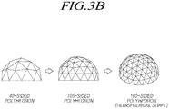
- the multi-display device 200 may constitute a polyhedron, which may be, for example, a 20-, 80-, 180-, 320-sided polyhedron, etc.
- the multi-display device 200 may have a spherical shape as a whole with an increase in the number of sides.
- the multi-display device 200 may constitute a hemispherical or domed polyhedron with three or more sides, which has two or more display devices 100 assembled together.
- the multi-display device 200 may constitute a hemispherical or domed polyhedron, which may be, for example, a 40-, 105-, 160-sided hemispherical or domed polyhedron, etc.
- the multi-display device 200 may have a hemispherical shape as a whole with an increase in the number of sides.
- the display panel 110 illustrated in FIG. 1 has a triangular shape, the degree of freedom in the manufacturing of a polyhedron may be increased, and it is possible to show images in consideration of future expandability.
- the display devices 100 constituting the polyhedron of the multi-display device 200 may operate in conjunction with each other to display content like a single image, or the display devices 100 may independently display images.
- FIG. 4 is a plan view of a display device according to another embodiment.
- the display device 400 may include a display panel 410, a driver 420, and a connector 430.
- the display panel 410 may include: multiple data lines DL and multiple gate lines GL arranged on a triangular substrate 412; and multiple pixels P disposed in a matrix form on the triangular substrate 412.
- the multiple pixels P may be arranged in the shape of a triangle on the triangular substrate 412.
- the triangular substrate 412 includes: three surfaces made up of first to third sides 412a, 412b, and 412c; and three vertices A, B, and C.
- the display panel 410 may be divided into an active area A/A for displaying an image and a non-active area N/A in which no image is displayed and elements relating to various types of signal lines or the driver 420 are arranged.
- Each of the multiple pixels P arranged in the display panel 410 may basically include: a display element (such as an organic light emitting diode (OLED) or liquid crystal cell); a driving transistor (DRT) for driving the display element; and a circuit element (such as a storage capacitor, etc.).
- a display element such as an organic light emitting diode (OLED) or liquid crystal cell
- DDT driving transistor
- a circuit element such as a storage capacitor, etc.
- each pixel may be diversely determined according to functions to be provided, design methods, and the like.
- the driver 420 may include: a data driver 422 that drives the multiple data lines DL by supplying data voltages to the multiple data lines DL; and a gate driver 424 that sequentially drives the multiple gate lines by sequentially supplying gate signals to the multiple gate lines.
- the data driver 422 may be connected to the display panel 410 by a tape automated bonding (TAB) method while being mounted on a data tape carrier package (TCP), or may be mounted on the display panel 410 by a chip-on-glass (COG) method.
- TAB tape automated bonding
- TCP data tape carrier package
- COG chip-on-glass
- the data driver 422 is supplied with control signals and driving voltages input from the outside through signal lines formed on a printed circuit board (PCB) connected to a TCP and is connected to the signal lines.
- PCB printed circuit board
- the gate driver 424 may be connected to a bonding pad of the display panel 410 by a tape automated bonding (TAB) method or a chip on glass (COG) method, or may be implemented in a gate in panel (GIP) type and directly disposed on the display panel 410. In some cases, the gate driver 424 may also be integrated into the display panel 410.
- TAB tape automated bonding
- COG chip on glass
- GIP gate in panel
- the gate driver 424 will be described as being implemented in a multi-gate in panel (GIP) type and directly disposed on the display panel 410.
- the gate driver 424 may sequentially supply gate signals from multiple gate-in-panels GIP through the multiple gate lines GL arranged on the display panel 410.
- the gate driver 424 may supply the gate signals in a forward or reverse direction through the multiple gate lines GL.
- the forward supply may mean that the gate signals are supplied to the gate lines GL close to the first side 412a and then to the gate lines GL away from the first side 412a, as illustrated in FIG. 2 .
- the reverse supply may mean that the gate signals are supplied to the gate lines GL away from the first side 412a and then to the gate lines GL close to the first side 412a, as illustrated in FIG. 2 .
- two triangular display devices 400 arranged in opposite directions may sequentially supply gate signals in reverse and forward directions, respectively, so that the multi-display device 200 may sequentially supply the gate signals in the same direction on the whole.
- the two triangular display devices 400 arranged in the opposite directions may sequentially supply gate signals in the same direction (that is, in the same reverse or forward direction) so that the multi-display device 200 may sequentially supply the gate signals in different directions for the respective unit display devices 400.
- the multiple data lines DL are arranged in a first direction from the first side 412a of the triangular substrate 412.
- the multiple data lines DL are arranged in the first direction from the first side 412a of the triangular substrate 412 to the second and third sides 412b and 412c of the substrate 412.
- the lengths of the multiple data lines DL may gradually increase and then decrease again from one end A to the other end B of the first side 412a of the substrate 412.
- the data lines DL on the central portion of the substrate 412 may have the largest lengths
- the data lines DL on opposite outer peripheral portions of the substrate 412 may have the smallest lengths. Accordingly, the data lines DL may have gradually decreasing lengths from the central portion toward the opposite outer peripheral portions of the substrate.
- the multiple gate lines GL are arranged between the second and third sides 412b and 412c of the triangular substrate 412 in a second direction, and the lengths of the multiple gate lines GL gradually decrease from one end A to the other end C of the second side 412b of the substrate 412.
- the pixels P are disposed in the areas where the multiple data lines DL arranged in the first direction and the multiple gate lines GL arranged in the second direction cross each other.
- the number of pixels P arranged in the active area A/A may gradually decrease away from the data driver 422 in proportion to the lengths of the gate lines that gradually decrease from one end A to the other end C of the second side 412b of the substrate 412.
- the multiple data lines DL and the multiple gate lines GL cross each other to form a triangular matrix as a whole, and the pixels P are disposed in the areas where the multiple data lines DL and the multiple gate lines GL cross each other. Accordingly, the multiple pixels P may be arranged in the shape of a triangle on the triangular substrate 412. When the multiple pixels P are arranged in the shape of a triangle on the triangular substrate 412, it means that the pixels P do not form a mathematically complete triangle, but has the shape of a triangle as a whole.
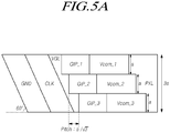
- FIG. 5A is a detailed view of the portion X of FIG. 4 , where FIG. 5A illustrates the arrangement of the gate driver and various types of interconnection wirings that are located in the non-active area of the substrate according to one embodiment.
- FIG. 5B is a detailed view illustrating the arrangement of the GIPs and pixels of FIG. 5A according to one embodiment.
- the gate driver 424 may include multiple gate-in-panels GIP arranged in the non-active area N/A of the display panel 410.
- the multiple gate-in-panels GIP may be arranged in the non-active area N/A so as to be parallel to one of the second and third sides 412b and 412c of the substrate 412.
- the multiple gate-in-panels GIP may also be arranged in the non-active area N/A so as to be parallel to both the second side 412b and the third side 412c of the substrate 412.
- gate-in-panels GIP may be disposed on opposite sides of each gate line GL, respectively, and one or both of the gate-in-panels GIP may supply a gate signal through the gate line GL.
- a ground wiring GND, a clock wiring CLK, and a gate voltage supply line VGL may be disposed between the multiple gate-in-panels GIP and the second side 412b of the substrate 412, and common wirings VCOM may be disposed between the gate-in-panels GIP and the pixels in the active area A/A.
- the arrangement of these wirings may be diversely modified.
- the ground wiring GND, the clock wiring CLK, and the common wirings VCOM may also be obliquely disposed.
- the oblique arrangement of the ground wiring GND, the clock wiring CLK, the gate voltage supply line VGL, the common wirings VCOM, and the multiple gate-in-panels GIP may be determined according to the triangular shape of the substrate 412. For example, in a case where the substrate 412 has the shape of an equilateral triangle, the ground wiring GND, the clock wiring CLK, the gate voltage supply line VGL, the common wirings VCOM, and the multiple gate-in-panels GIP may be obliquely disposed parallel to the second or third side 412b or 412c of the substrate 412.
- the multiple gate-in-panels GIP may be obliquely disposed in the direction from one end A to the other end C of the second side 412b of the substrate 412 with a pitch of a / b ( a and b are real numbers greater than 0) inward from the second side 412b of the substrate 412.
- the multiple gate-in-panels GIP may be obliquely disposed in the direction from one end B to the other end C of the third side 412c of the substrate 412 with a pitch of a / b inward from the third side 412c of the substrate 412.
- b may be determined according to the triangular shape of the substrate 412.
- the multiple gate-in-panels GIP may be obliquely disposed in the direction from one end B to the other end C of the third side 412c of the substrate 412, for example, with a pitch of a / 3 inward from the third side 412c of the substrate 412, but is not limited thereto.
- one gate line GL may be used to simultaneously supply gate signals for two pixels P located on opposite sides thereof.
- the height a of the gate-in-panels GIP may be the same, or substantially the same, as the width of the two pixels located on the opposite sides of the gate line.
- the height a of the gate-in-panels GIP may be the same, or substantially the same, as the width of the pixel P.
- three pixels in the second direction may be obliquely disposed toward the interior of the substrate 412 with the same pitch as that of the multiple gate-in-panels GIP mentioned above, or with a pitch that is not the same as that of the multiple gate-in-panels GIP.
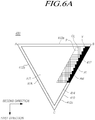
- FIGS. 6A to 6C are plan views illustrating the arrangement of a black matrix included in a liquid crystal display device when the display device of FIG. 4 is a liquid crystal display device according to one embodiment.
- FIG. 6A only a part Y of the active and non-active areas is illustrated in detail, and other parts are omitted.
- the display device 400 may further include a black matrix BM that is disposed on another substrate (not illustrated) facing the substrate 410 to correspond the non-active area N/A and a driving area in which thin film transistors (TFTs) are disposed in the active area A/A to drive the data lines DL, the gate lines GL, and the pixels P.
- the black matrix BM may cover the non-active area N/A and the driving area of the active area A/A.
- pixels PI located at the boundary 414 between the triangular active area A/A and the non-active area N/A may each cover a part of the active area A/A and a part of the non-active area N/A.
- some pixels PI are divided by the boundary 414 between the active area A/A and the non-active area N/A.
- the black matrix BM may have a structure in which the black matrix BM covers all the pixels PI located at the boundary 414.
- the black matrix BM may have an outer periphery that follows the shapes of the active areas A/A of the pixels PI that are divided by the boundary 414.
- the black matrix BM may extend from the non-active area N/A to the boundary 414 between the active area A/A and the non-active area N/A.
- the black matrix BM may have a structure in which the black matrix BM only covers the portions that are included in the pixels PI located at the boundary 414 and are located in the non-active area N/A.
- two or more pixels PI located in the outermost positions so as to be adjacent to the second side 412b of the substrate 412 may be obliquely disposed inside the second side 412b of the substrate 412.
- two or more pixels PI located in the outermost positions so as to be adjacent to the third side 412c of the substrate 412 may be obliquely disposed inside the third side 412c of the substrate 412.
- the black matrix BM may obliquely cover a part of each of the pixels PI located in the outermost positions so as to be adjacent to the second and third sides 412b and 412c of the substrate 412. Accordingly, the boundary 414 that distinguishes between the active area A/A and the non-active area N/A agrees with the inclined line of the black matrix BM. While it will be exemplified that the boundary 414 that distinguishes between the active area A/A and the non-active area N/A agrees with the inclined line of the black matrix BM, the boundary 414 may not agree with the inclined line of the black matrix BM.
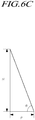
- the angle ⁇ of the inclined line of the black matrix BM which covers a part of each pixel PI, may be an arctangent ( H / P ) with respect to the first side 412a.
- the width P of the three pixels P in the first direction is equal to D
- the height H of the two pixels P located on the opposite sides of the gate line may be smaller than or equal to 2D.
- the angle ⁇ of the inclined line of the black matrix BM which covers a part of each pixel PI, may be less than or equal to 63.4 because the angle ⁇ is an arctangent ( H / P ) with respect to the first side 412a.
- the angle ⁇ of the inclined line of the black matrix BM may be 60 degrees with respect to the first side 412a of the substrate 412, but is not limited thereto.
- a step pattern may not be recognized at the boundary 414 between the active area A/A and the non-active area N/A.
- FIGS. 7A and 7B are plan views illustrating another embodiment of the arrangement of a black matrix included in a liquid crystal display device when the display device of FIG. 4 is a liquid crystal display device.
- the inclined line of the black matrix BM (that is, the boundary 414 between the active area A/A and the non-active area N/A) may be parallel to the diagonal line that connects vertices of one or more pixels PI located in the outermost positions so as to be adjacent to the second or third side 412b or 412c of the substrate 412.
- the inclined line of the black matrix BM may be parallel to the diagonal line that connects vertices of one pixel PI located in the outermost position so as to be adjacent to the second or third side 412b or 412c of the substrate 412.
- the inclined line of the black matrix BM may be identical to the diagonal line that connects the vertices of the pixel PI located in the outermost position so as to be adjacent to the second or third side 412b or 412c of the substrate 412.
- the black matrix BM may cover one half of the pixel PI located in the outermost position so as to be adjacent to the second or third side 412b or 412c of the substrate 412.
- the inclined line of the black matrix BM may be parallel to the diagonal line that connects vertices of two pixels PI located in the outermost positions so as to be adjacent to the second or third side 412b or 412c of the substrate 412.
- the inclined line of the black matrix BM may be identical to the diagonal line that connects the vertices of the two pixels PI located in the outermost positions so as to be adjacent to the second or third side 412b or 412c of the substrate 412.
- the black matrix BM may cover one half of the two pixels PI located in the outermost positions so as to be adjacent to the second or third side 412b or 412c of the substrate 412.
- the inclined line of the black matrix BM is parallel to the diagonal line that connects the vertices of one or two pixels PI located in the outermost positions so as to be adjacent to the second or third side 412b or 412c of the substrate 412
- the inclined line of the black matrix BM may be parallel to the diagonal line that connects vertices of three or more pixels PI located in the outermost positions so as to be adjacent to the second or third side 412b or 412c of the substrate 412.
- the inclined line of the black matrix BM may be identical to the diagonal line that connects the vertices of the three or more pixels PI located in the outermost positions so as to be adjacent to the second or third side 412b or 412c of the substrate 412. Accordingly, the black matrix BM may cover one half of the three or more pixels PI located in the outermost positions so as to be adjacent to the second or third side 412b or 412c of the substrate 412.
- the aspect ratio of the pixels may be specified. That is, the aspect ratio of the pixels may be determined according to the shape of the triangle.
- the ratio of the length b in the second direction to the length a in the first direction may be 1: 3 / n for each of the pixels located in the outermost positions so as to be adjacent to the second and third sides 412b and 412c of the substrate 412 (n is the number of minimum outermost pixels, the vertices of which the inclined line of the black matrix BM passes through), but is not limited thereto.
- a step pattern may not be recognized at the boundary 414 between the active area A/A and the non-active area N/A.
- FIG. 8 illustrates image processing (blurring) of pixels P on a boundary portion 416 located in the active area A/A of the display panel 410 illustrated in FIG. 4 and located at the boundary between the active area A/A and the non-active area N/A in order to prevent a step pattern from being recognized at the boundary 414 between an active area A/A and a non-active area N/A.
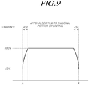
- the pixels P on the boundary portion 416 may have relatively low luminance as illustrated in FIG. 9 .
- the pixels P located on the boundary portion 416 adjacent to the second and third sides 412b and 412c of the substrate 412 may have lower luminance than that of the pixels P located on the central portion of the substrate 412.
- the luminance of the pixels P located on the boundary portion 416 adjacent to the second and third sides 412b and 412c of the substrate 412 may decrease gradually or in a stepwise manner with an approach to the outermost pixel P.
- the pixels P located on the central portion of the substrate 412 has luminance of 100%
- the pixels P located on the boundary portion 416 adjacent to the second and third sides 412b and 412c of the substrate 412 may have, for example, luminance of 50%, but may have any value lower than 100% without being limited thereto.
- the number of pixels P disposed on the boundary portion 416, a luminance reduction rate, and the luminance of the outermost pixel may be properly selected according to various situations of the display device 400.
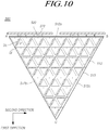
- FIGS. 10 and 11 are plan views of a display device according to yet another embodiment.
- the display device 500 may include a display panel 510, a driver 520, and a connector 530.
- Multiple pixels P disposed in the areas of the display panel 510 where data lines DL and gate lines GL cross each other may have a triangular shape.
- Two triangular pixels adjacent to each other in a second direction may be arranged in opposite directions to form a parallelogram as a whole. Accordingly, a step pattern is not recognized at the boundary between an active area and a non-active area.
- the data lines DL may be arranged so as to be inclined with respect to a first direction, and the gate lines GL may be arranged parallel to the second direction.
- the triangular shape of the multiple pixels P may be similar to that of a substrate 412, but is not limited thereto.
- the multiple pixels P may also have the shape of an equilateral triangle.
- three pixels P arranged in the second direction and one pixel P adjacent thereto in the first direction may be repetitively disposed in a triangular shape.
- the four pixels repetitively disposed in a triangular shape may include red (R), blue (B), green (G), and white (W) pixels.
- the red (R), blue (B), green (G), and white (W) pixels may represent one color.
- FIG. 12 illustrates alignment layers of pixels P1 and P2 included in a liquid crystal display device and the directions of liquid crystals when the liquid crystals are driven in a case where the display device of FIG. 10 is a liquid crystal display device.
- the directions of the alignment layers 519 of the two adjacent liquid crystal cells P1 and P2 may differ from each other. Accordingly, the liquid crystals 518, when being driven, may rotate in different directions so that the two liquid crystal cells P1 and P2 may operate as different domains.
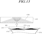
- FIG. 13 is a plan view illustrating a part of a display panel in a display device according to yet another embodiment.
- the display device 600 may further include: a data pad unit (not illustrated) that includes multiple data pads disposed in the non-active area N/A directed toward a first side 612a of a substrate 612; and a data link line unit 619 that includes multiple data link lines 619a that connect the data pad unit and data lines DL.
- the multiple data link lines 619a included in the data link line unit 619 may have the same length.
- data link lines 619a located on the central portion may each have a part disposed in zigzags in the non-active area N/A of the display panel 610. Accordingly, the lengths of the data link lines 619a from the data pads (not illustrated) to the data lines DL may be equal to each other on the central portion and the outer peripheral portions.
- the total length of the data lines DL and the data link lines 619a on the central portion may be shorter than that of the data lines DL and the data link lines 619a on the outer peripheral portions. Accordingly, the line resistance of the data lines DL located on the central portion may be greater than that of the data lines DL located on the outer peripheral portions.
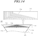
- FIG. 14 is a plan view illustrating a part of a display panel in a display device according to yet another embodiment.
- the display device(700), according to this embodiment, may further include: a data pad unit (not illustrated) that includes multiple data pads disposed in the non-active area N/A directed toward a first side 712a of a substrate 712; and a data link line unit 719 that includes multiple data link lines 719a that connect the data pad unit and data lines DL.
- the lengths of the multiple data link lines 719a included in the data link line unit 719 may gradually decrease and then increase from one end A to the other end B of the first side 712a of the substrate 712. In other words, the lengths of the multiple data link lines 719a on the peripheral portions may be greater than those of the multiple data link lines 719a on the central portion.
- the total length of the data lines DL and the data link lines 719a may be constant. Accordingly, the line resistance of the data lines DL located on the central portion and the outer peripheral portions may be constant in the active area A/A.
- a multi-display device may be manufactured by combining two or more of the display devices according to the embodiments mentioned above.
- the multi-display devices may continuously display one image in three dimensions.
Landscapes
- Physics & Mathematics (AREA)
- Engineering & Computer Science (AREA)
- General Physics & Mathematics (AREA)
- Theoretical Computer Science (AREA)
- Nonlinear Science (AREA)
- Chemical & Material Sciences (AREA)
- Crystallography & Structural Chemistry (AREA)
- Computer Hardware Design (AREA)
- Mathematical Physics (AREA)
- Optics & Photonics (AREA)
- General Engineering & Computer Science (AREA)
- Multimedia (AREA)
- Human Computer Interaction (AREA)
- Geometry (AREA)
- Devices For Indicating Variable Information By Combining Individual Elements (AREA)
- Liquid Crystal (AREA)
- Electroluminescent Light Sources (AREA)
Abstract
Description
- This application claims priority from
Korean Patent Application No. 10-2016-0142996, filed on October 31,2016 - Embodiments of the present disclosure relate to a display device for displaying an image and a multi-display device implemented as a polyhedron through a combination of display devices.
- With the development of information society, various types of requirements for display devices to display images have increased, and various types of display devices have recently been used, such as a liquid crystal display (LCD), a plasma display panel (PDP), an organic light emitting diode display device (OLED), and the like.
- In general, display devices have rectangular display panels. These general display devices may be combined to continuously display images on a large screen, but may have a limitation in implementing a polyhedron to continuously display images in three dimensions.
- An aspect of the present disclosure is to provide a display device used for manufacturing a multi-display device.
- Another aspect of the present disclosure is to provide a multi-display device capable of continuously displaying one image in three dimensions.
- In accordance with an aspect of the present disclosure, there is provided a display device that comprises: a triangular display panel including: a triangular substrate; a plurality of data lines on the triangular substrate; a plurality of gate lines on the triangular substrate; a plurality of pixels disposed in a plurality of rows on the triangular substrate; a data driver located along a first side of the triangular substrate, the data driver supplying data voltages to the plurality of data lines; and a gate driver located along the first side of the triangular substrate, the gate driver sequentially supplying gate signals to the plurality of gate lines, wherein a number of pixels in each of the plurality of rows decreases as a distance between each row and the first side of the triangular substrate increases.
- In accordance with another aspect of the present disclosure, there is provided a multi-display device with four or more surfaces and the multi-display device including a plurality of display devices assembled together through a connecting member to form the multi-display device, wherein each display device comprises: a triangular display panel including: a triangular substrate; a plurality of data lines on the triangular substrate; a plurality of gate lines on the triangular substrate; a plurality of pixels disposed in a plurality of rows on the triangular substrate, the plurality of pixels arranged in a shape of a triangle on the triangular substrate; a data driver located along a first side of the triangular substrate, the data driver supplying data voltages to the plurality of data lines; and a gate driver located along the first side of the triangular substrate, the gate driver sequentially supplying gate signals to the plurality of gate lines, wherein a number of pixels in each of the plurality of rows decreases as a distance between each row and the first side of the triangular substrate increases.
- According to the embodiments of the present invention, the display device may be used to manufacture a multi-display device.
- In addition, according to the embodiments of the present invention, the multi-display device may continuously display one image in three dimensions.
- Various embodiments provide a display device comprising: a triangular display panel including: a triangular substrate; a plurality of data lines on the triangular substrate; a plurality of gate lines on the triangular substrate; a plurality of pixels disposed in a plurality of rows on the triangular substrate; a data driver located along a first side of the triangular substrate, the data driver supplying data voltages to the plurality of data lines; and a gate driver located along the first side of the triangular substrate, the gate driver sequentially supplying gate signals to the plurality of gate lines, wherein a number of pixels in each of the plurality of rows decreases as a distance between each row and the first side of the triangular substrate increases.
- In one or more embodiments, the plurality of data lines are arranged in a first direction from the first side of the triangular substrate, and lengths of the plurality of data lines increase from a first end of the first side of the triangular substrate toward a center of the first side of the triangular substrate, and the lengths of the plurality of data lines decrease from the center of the first side of the triangular substrate towards a second end of the first side of the triangular substrate, wherein the plurality of gate lines are arranged between a second side and a third side of the triangular substrate in a second direction intersecting the first direction, and lengths of the plurality of gate lines decrease as a distance from each gate line to the first side of the triangular substrate increases.
- In one or more embodiments, the gate driver comprises a plurality of gate-in-panels, and the plurality of gate-in-panels are disposed at the second side or the third side of the triangular substrate, and the plurality of gate-in-panels are parallel with the second side or the third side of the triangular substrate.
- In one or more embodiments, the plurality of gate-in-panels each comprisea height of a, and the triangular substrate comprises a shape of an equilateral triangle, and the plurality of gate-in-panels are obliquely arranged in a direction from a first end of either the second side or the third side of the triangular substrate to a second end of either the second side or third side of the triangular substrate with a pitch of a/b (a and b are real numbers greater than 0) inward from either the second side or third side of the triangular substrate.
- In one or more embodiments, two or more pixels from the plurality of pixels that are located at an edge of a second side of the triangular substrate are obliquely arranged at the edge of the second side of the triangular substrate, wherein two or more pixels from the plurality of pixels that are located at an edge of a third side of the triangular substrate are obliquely arranged at the edge of the third side of the triangular substrate, and the display device further comprises a black matrix that obliquely covers a part of each of the two pixels located at the edge of the second side of the triangular substrate and the black matrix obliquely covers a part of each of the two pixels located at the edge of the third side of the triangular substrate.
- In one or more embodiments, an angle of inclined lines of the black matrix is smaller than or equal to 63.4 degrees with respect to the first side of the triangular substrate.
- In one or more embodiments, inclined lines of the black matrix are parallel to directions defined by vertices at corners of one or more pixels located at the edges of the second side and the third side of the triangular substrate.
- In one or more embodiments, the inclined lines of the black matrix pass through the vertices at the corners of the one or more pixels located at the edges of the second side and the third side of the triangular substrate.
- In one or more embodiments, the triangular substrate has a shape of an equilateral triangle, and a ratio of a length in the second direction and a length in the first direction is 1:

- In one or more embodiments, two or more pixels from the plurality of pixels that are located at an edge of a second side of the triangular substrate are obliquely arranged at the second side of the triangular substrate, wherein two or more pixels from the plurality of pixels that are located at an edge of a third side of the triangular substrate are obliquely arranged at the edge of the third side of the triangular substrate, and wherein a luminance of the two or more pixels located at the edges of the second side and the third side of the triangular substrate are lower than a luminance of pixels located at a central portion of the substrate.
- In one or more embodiments, the luminance of the pixels located at the edges of the second side and the third side of the triangular substrate gradually decreases towards the edge of the second side and the third side of the triangular substrate.
- In one or more embodiments, each of the plurality of pixels has a triangular shape, and two adjacent pixels in the second direction form a parallelogram.
- In one or more embodiments, the triangular shape of the plurality of pixels is similar to a shape of the triangular substrate.
- In one or more embodiments, three pixels arranged in the second direction and one pixel adjacent to the three pixels in the first direction are repetitively disposed in a triangular shape.
- In one or more embodiments, the four pixels repetitively disposed in the triangular shape comprise a red pixel, a blue pixel, a green pixel, and a white pixel.
- In one or more embodiments, the two adjacent pixels are liquid crystal cells, and directions of alignment layers of the two adjacent pixels are different from each other.
- In one or more embodiments, the display panel further comprises: a data pad unit that comprises a plurality of data pads is in a non-active area of the display panel that does not display an image, the data pad unit located at the first side of the triangular substrate; and a data link line unit that comprises a plurality of data link lines, the plurality of data link lines connecting together the data pad unit and the plurality of data lines, and wherein lengths of the plurality of data link lines decrease from the first end of the first side of the triangular substrate toward the center of the first side of the triangular substrate, and the lengths of the plurality of data link lines increase from the center of the first side of the triangular substrate towards the second end of the first side of the triangular substrate.
- In one or more embodiments, a row of pixels closest to the first side of the triangular substrate includes the highest number of complete pixels in the display device.
- Various embodiments provide a multi-display device with four or more surfaces and the multi-display device includes a plurality of display devices according to one or more embodiments described herein, assembled together through a connecting member to form the multi-display device.
- In one or more embodiments, the multi-display device has one of a polyhedral shape, a spherical shape, or a hemispherical shape.
- Various embodiments provide a multi-display device with four or more surfaces and the multi-display device including a plurality of display devices assembled together through a connecting member to form the multi-display device, wherein each display device comprises: a triangular display panel including: a triangular substrate; a plurality of data lines on the triangular substrate; a plurality of gate lines on the triangular substrate; a plurality of pixels disposed in a plurality of rows on the triangular substrate, the plurality of pixels arranged in a shape of a triangle on the triangular substrate; a data driver located along a first side of the triangular substrate, the data driver supplying data voltages to the plurality of data lines; and a gate driver located along the first side of the triangular substrate, the gate driver sequentially supplying gate signals to the plurality of gate lines, wherein a number of pixels in each of the plurality of rows decreases as a distance between each row and the first side of the triangular substrate increases.
- In one or more embodiments, the multi-display device has one of a polyhedral shape, a spherical shape, or a hemispherical shape.
- The above and other objects, features, and advantages of the present invention will be more apparent from the following detailed description taken in conjunction with the accompanying drawings, in which:
-
FIG. 1 is a plan view of a display device according to one embodiment. -
FIG. 2 is a development view of a multi-display device having a plurality of display devices assembled together, each of which is illustrated inFIG. 1 according to one embodiment. -
FIGS. 3A and3B are perspective views of the multi-display device ofFIG. 2 , which is assembled in a polyhedron structure according to one embodiment. -
FIG. 4 is a plan view of a display device according to another embodiment. -
FIG. 5A is a detailed view of the portion X ofFIG. 4 , whereFIG. 5A illustrates the arrangement of a gate driver and various types of interconnection wirings that are located in the non-active area of a substrate according to one embodiment. -
FIG. 5B is a detailed view illustrating the arrangement of GIPs and pixels ofFIG. 5A according to one embodiment. -
FIGS. 6A to 6C are plan views illustrating one embodiment of the arrangement of a black matrix included in a liquid crystal display device when the display device ofFIG. 4 is a liquid crystal display device according to one embodiment. -
FIGS. 7A and7B are plan views illustrating another embodiment of the arrangement of a black matrix included in a liquid crystal display device when the display device ofFIG. 4 is a liquid crystal display device according to one embodiment. -
FIG. 8 illustrates image processing of diagonal pixels located at the boundary between an active area A/A and a non-active area N/A according to one embodiment. -
FIG. 9 illustrates relative luminance of pixels on central and diagonal portions according to one embodiment. -
FIGS. 10 and11 are plan views of a display device according to yet another embodiment. -
FIG. 12 illustrates alignment layers of pixels included in a liquid crystal display device and the directions of liquid crystals when the liquid crystals are driven in a case where the display device ofFIG. 10 is a liquid crystal display device according to one embodiment. -
FIG. 13 is a plan view illustrating a part of a display panel in a display device according to yet another embodiment. -
FIG. 14 is a plan view illustrating a part of a display panel in a display device according to yet another embodiment. - Hereinafter, some embodiments of the present invention will be described in detail with reference to the accompanying illustrative drawings. In designating elements of the drawings by reference numerals, the same elements will be designated by the same reference numerals although they are shown in different drawings. Further, in the following description of the present invention, a detailed description of known functions and configurations incorporated herein will be omitted when it may make the subject matter of the present invention rather unclear.
- In addition, terms, such as first, second, A, B, (a), (b) or the like may be used herein when describing components of the present invention. Each of these terminologies is not used to define an essence, order or sequence of a corresponding component but used merely to distinguish the corresponding component from other component(s). In the case that it is described that a certain structural element "is connected to", "is coupled to", or "is in contact with" another structural element, it should be interpreted that another structural element may be connected to", "be coupled to", or "be in contact with" the structural elements as well as that the certain structural element is directly connected to or is in direct contact with another structural element.
-
FIG. 1 is a plan view of a display device according to one embodiment. - Referring to
FIG. 1 , thedisplay device 100, according to the embodiment, includes atriangular display panel 110, adriver 120 for driving thedisplay panel 110, and aconnector 130 located between thedisplay panel 110 and thedriver 120. Examples of thedisplay device 100 may include various current or upcoming display devices, such as a liquid crystal display (LCD), a plasma display panel (PDP), an organic light emitting diode (OLED) display device, and the like. - The
display panel 110 may independently display an image in the shape of a triangle, or may be coupled with another display device to display a continuous image. Thedisplay panel 110 may have the shape of a triangle, such as an equilateral triangle or an isosceles triangle, but is not limited thereto. - When the
display panel 110 has a triangular shape, it means that thedisplay panel 110 has the shape of a triangle as a whole. Accordingly, three sides of thedisplay panel 110 may be mathematically curvilinear rather than linear, or the distal ends of all or some of the three sides may be bent. Furthermore, some of vertices of thedisplay panel 110 may be cut away or may be rounded. Hereinafter, it will be exemplified that thedisplay panel 110 has the shape of a mathematical triangle. - The
driver 120 may be located on one surface of thedisplay panel 110 and may drive or control thedisplay panel 110 through theconnector 130. Thedriver 120 may be one, or a combination, of a data driver, a gate driver, a controller for controlling the data and gate drivers, and a touch driver of a general display device. While thedriver 120 will be hereinafter described as including a data driver and a gate driver, thedriver 120 is not limited thereto. - The
connector 130 is located between thedisplay panel 110 and thedriver 120 and transmits a drive signal and/or a control signal of thedriver 120 to thedisplay panel 110. Theconnector 130 may connect thedisplay panel 110 and thedriver 120, for example, through tape automated bonding (TAB). - The
driver 120 may be connected to a bonding pad of thedisplay panel 110 by a chip-on-glass (COG) method, or may be directly mounted on thedisplay panel 110. Alternatively, thedriver 120 may be mounted on thedisplay panel 110 through integration. In this case, thedisplay device 100 may not include theseparate connector 130. -
FIG. 2 is a development view of a multi-display device having a plurality of display devices assembled together, each of which is illustrated inFIG. 1 according to one embodiment. - Referring to
FIG. 2 , themulti-display device 200, according one embodiment, may have thedisplay device 100 ofFIG. 1 as a unit display device, and two ormore display devices 100 may be assembled together through connecting members (not illustrated). Eachdisplay device 100 may include adisplay panel 110, adriver 120, and aconnector 130, as illustrated inFIG. 1 . In this case, twoadjacent display devices 100 in themulti-display device 200 may form a parallelogram, and the surfaces of thedisplay devices 100 on which thedrivers 120 are located may constitute the two bases of the parallelogram. - The
multi-display device 200, as illustrated inFIG. 3A , may constitute a polyhedron with three or more sides, which has two ormore display devices 100 assembled together. Themulti-display device 200 may constitute a polyhedron, which may be, for example, a 20-, 80-, 180-, 320-sided polyhedron, etc. Themulti-display device 200 may have a spherical shape as a whole with an increase in the number of sides. - The
multi-display device 200, as illustrated inFIG. 3B , may constitute a hemispherical or domed polyhedron with three or more sides, which has two ormore display devices 100 assembled together. Themulti-display device 200 may constitute a hemispherical or domed polyhedron, which may be, for example, a 40-, 105-, 160-sided hemispherical or domed polyhedron, etc. Themulti-display device 200 may have a hemispherical shape as a whole with an increase in the number of sides. - Since the
display panel 110 illustrated inFIG. 1 has a triangular shape, the degree of freedom in the manufacturing of a polyhedron may be increased, and it is possible to show images in consideration of future expandability. Thedisplay devices 100 constituting the polyhedron of themulti-display device 200 may operate in conjunction with each other to display content like a single image, or thedisplay devices 100 may independently display images. - Hereinafter, specific embodiments of the
unit display device 100 will be described in detail with reference to the accompanying drawings. -
FIG. 4 is a plan view of a display device according to another embodiment. - Referring to
FIG. 4 , thedisplay device 400, according to the other embodiment, may include adisplay panel 410, adriver 420, and aconnector 430. - The
display panel 410 may include: multiple data lines DL and multiple gate lines GL arranged on atriangular substrate 412; and multiple pixels P disposed in a matrix form on thetriangular substrate 412. The multiple pixels P may be arranged in the shape of a triangle on thetriangular substrate 412. Thetriangular substrate 412 includes: three surfaces made up of first tothird sides display panel 410 may be divided into an active area A/A for displaying an image and a non-active area N/A in which no image is displayed and elements relating to various types of signal lines or thedriver 420 are arranged. - Each of the multiple pixels P arranged in the
display panel 410, according to this embodiment, may basically include: a display element (such as an organic light emitting diode (OLED) or liquid crystal cell); a driving transistor (DRT) for driving the display element; and a circuit element (such as a storage capacitor, etc.). - The types and number of circuit elements constituting each pixel may be diversely determined according to functions to be provided, design methods, and the like.
- The
driver 420 may include: adata driver 422 that drives the multiple data lines DL by supplying data voltages to the multiple data lines DL; and agate driver 424 that sequentially drives the multiple gate lines by sequentially supplying gate signals to the multiple gate lines. - The
data driver 422 may be connected to thedisplay panel 410 by a tape automated bonding (TAB) method while being mounted on a data tape carrier package (TCP), or may be mounted on thedisplay panel 410 by a chip-on-glass (COG) method. Hereinafter, it will be exemplified that thedata driver 422 is supplied with control signals and driving voltages input from the outside through signal lines formed on a printed circuit board (PCB) connected to a TCP and is connected to the signal lines. - The
gate driver 424 may be connected to a bonding pad of thedisplay panel 410 by a tape automated bonding (TAB) method or a chip on glass (COG) method, or may be implemented in a gate in panel (GIP) type and directly disposed on thedisplay panel 410. In some cases, thegate driver 424 may also be integrated into thedisplay panel 410. - Hereinafter, the
gate driver 424 will be described as being implemented in a multi-gate in panel (GIP) type and directly disposed on thedisplay panel 410. Thegate driver 424 may sequentially supply gate signals from multiple gate-in-panels GIP through the multiple gate lines GL arranged on thedisplay panel 410. - The
gate driver 424 may supply the gate signals in a forward or reverse direction through the multiple gate lines GL. In this case, the forward supply may mean that the gate signals are supplied to the gate lines GL close to thefirst side 412a and then to the gate lines GL away from thefirst side 412a, as illustrated inFIG. 2 . The reverse supply may mean that the gate signals are supplied to the gate lines GL away from thefirst side 412a and then to the gate lines GL close to thefirst side 412a, as illustrated inFIG. 2 . - Accordingly, in a
multi-display device 200 that includes thedisplay device 400 illustrated inFIG. 4 as a unit display device, twotriangular display devices 400 arranged in opposite directions may sequentially supply gate signals in reverse and forward directions, respectively, so that themulti-display device 200 may sequentially supply the gate signals in the same direction on the whole. In themulti-display device 200, the twotriangular display devices 400 arranged in the opposite directions may sequentially supply gate signals in the same direction (that is, in the same reverse or forward direction) so that themulti-display device 200 may sequentially supply the gate signals in different directions for the respectiveunit display devices 400. - The multiple data lines DL are arranged in a first direction from the
first side 412a of thetriangular substrate 412. In other words, the multiple data lines DL are arranged in the first direction from thefirst side 412a of thetriangular substrate 412 to the second andthird sides substrate 412. In this case, the lengths of the multiple data lines DL may gradually increase and then decrease again from one end A to the other end B of thefirst side 412a of thesubstrate 412. In other words, the data lines DL on the central portion of thesubstrate 412 may have the largest lengths, and the data lines DL on opposite outer peripheral portions of thesubstrate 412 may have the smallest lengths. Accordingly, the data lines DL may have gradually decreasing lengths from the central portion toward the opposite outer peripheral portions of the substrate. - The multiple gate lines GL are arranged between the second and
third sides triangular substrate 412 in a second direction, and the lengths of the multiple gate lines GL gradually decrease from one end A to the other end C of thesecond side 412b of thesubstrate 412. - As illustrated in
FIG. 4 , the pixels P are disposed in the areas where the multiple data lines DL arranged in the first direction and the multiple gate lines GL arranged in the second direction cross each other. The pixels P in the active area A/A of thedisplay panel 410 that are adjacent to thefirst side 412a of thesubstrate 412, at which thedata driver 422 is disposed, are arranged parallel to thedata driver 422. The number of pixels P arranged in the active area A/A may gradually decrease away from thedata driver 422 in proportion to the lengths of the gate lines that gradually decrease from one end A to the other end C of thesecond side 412b of thesubstrate 412. - The multiple data lines DL and the multiple gate lines GL cross each other to form a triangular matrix as a whole, and the pixels P are disposed in the areas where the multiple data lines DL and the multiple gate lines GL cross each other. Accordingly, the multiple pixels P may be arranged in the shape of a triangle on the
triangular substrate 412. When the multiple pixels P are arranged in the shape of a triangle on thetriangular substrate 412, it means that the pixels P do not form a mathematically complete triangle, but has the shape of a triangle as a whole. -
FIG. 5A is a detailed view of the portion X ofFIG. 4 , whereFIG. 5A illustrates the arrangement of the gate driver and various types of interconnection wirings that are located in the non-active area of the substrate according to one embodiment.FIG. 5B is a detailed view illustrating the arrangement of the GIPs and pixels ofFIG. 5A according to one embodiment. - Referring to
FIGS. 5A and5B , thegate driver 424 may include multiple gate-in-panels GIP arranged in the non-active area N/A of thedisplay panel 410. The multiple gate-in-panels GIP may be arranged in the non-active area N/A so as to be parallel to one of the second andthird sides substrate 412. - Alternatively, the multiple gate-in-panels GIP may also be arranged in the non-active area N/A so as to be parallel to both the
second side 412b and thethird side 412c of thesubstrate 412. In other words, gate-in-panels GIP may be disposed on opposite sides of each gate line GL, respectively, and one or both of the gate-in-panels GIP may supply a gate signal through the gate line GL. - A ground wiring GND, a clock wiring CLK, and a gate voltage supply line VGL may be disposed between the multiple gate-in-panels GIP and the
second side 412b of thesubstrate 412, and common wirings VCOM may be disposed between the gate-in-panels GIP and the pixels in the active area A/A. However, the arrangement of these wirings may be diversely modified. Likewise to the multiple gate-in-panels GIP, the ground wiring GND, the clock wiring CLK, and the common wirings VCOM may also be obliquely disposed. The oblique arrangement of the ground wiring GND, the clock wiring CLK, the gate voltage supply line VGL, the common wirings VCOM, and the multiple gate-in-panels GIP may be determined according to the triangular shape of thesubstrate 412. For example, in a case where thesubstrate 412 has the shape of an equilateral triangle, the ground wiring GND, the clock wiring CLK, the gate voltage supply line VGL, the common wirings VCOM, and the multiple gate-in-panels GIP may be obliquely disposed parallel to the second orthird side substrate 412. - In a case where the multiple gate-in-panels GIP have a height of a, and the
substrate 412 has the shape of an equilateral triangle, the multiple gate-in-panels GIP may be obliquely disposed in the direction from one end A to the other end C of thesecond side 412b of thesubstrate 412 with a pitch of a/b (a and b are real numbers greater than 0) inward from thesecond side 412b of thesubstrate 412. In a case where the multiple gate-in-panels GIP are arranged parallel to thethird side 412c of thesubstrate 412, the multiple gate-in-panels GIP may be obliquely disposed in the direction from one end B to the other end C of thethird side 412c of thesubstrate 412 with a pitch of a/b inward from thethird side 412c of thesubstrate 412. In this case, b may be determined according to the triangular shape of thesubstrate 412. - For example, in a case where the
substrate 412 has the shape of an equilateral triangle, and the ground wiring GND, the clock wiring CLK, the common wirings VCOM, and the multiple gate-in-panels GIP are obliquely disposed with an angle of 60 degrees relative to thefirst side 412a, the multiple gate-in-panels GIP may be obliquely disposed in the direction from one end B to the other end C of thethird side 412c of thesubstrate 412, for example, with a pitch of
third side 412c of thesubstrate 412, but is not limited thereto. - As illustrated in
FIG. 5B , one gate line GL may be used to simultaneously supply gate signals for two pixels P located on opposite sides thereof. In this case, the height a of the gate-in-panels GIP may be the same, or substantially the same, as the width of the two pixels located on the opposite sides of the gate line. Meanwhile, in a case where a gate signal is supplied to one pixel P through one gate line, the height a of the gate-in-panels GIP may be the same, or substantially the same, as the width of the pixel P. - When one gate line is used to supply gate signals for two pixels P located on opposite sides thereof, three pixels in the second direction (that is, 2 x 3 pixels (a total of 6 pixels)) may be obliquely disposed toward the interior of the
substrate 412 with the same pitch as that of the multiple gate-in-panels GIP mentioned above, or with a pitch that is not the same as that of the multiple gate-in-panels GIP. -
FIGS. 6A to 6C are plan views illustrating the arrangement of a black matrix included in a liquid crystal display device when the display device ofFIG. 4 is a liquid crystal display device according to one embodiment. InFIG. 6A , only a part Y of the active and non-active areas is illustrated in detail, and other parts are omitted. - Referring to
FIG. 6A , in a case where thedisplay device 400 described above with reference toFIG. 4 is a liquid crystal display device, thedisplay device 400 may further include a black matrix BM that is disposed on another substrate (not illustrated) facing thesubstrate 410 to correspond the non-active area N/A and a driving area in which thin film transistors (TFTs) are disposed in the active area A/A to drive the data lines DL, the gate lines GL, and the pixels P. The black matrix BM may cover the non-active area N/A and the driving area of the active area A/A. - Among the multiple pixels P disposed, as described above, in the areas in which the multiple data lines DL directed in the first direction and the multiple gate lines GL directed in the second direction cross each other, pixels PI located at the
boundary 414 between the triangular active area A/A and the non-active area N/A may each cover a part of the active area A/A and a part of the non-active area N/A. In particular, when the pixels PI located at theboundary 414 between the active area A/A and the non-active area N/A have the same pixel structure as that of the pixels P located in the active area A/A, some pixels PI are divided by theboundary 414 between the active area A/A and the non-active area N/A. - As illustrated in
FIG. 6A , the black matrix BM may have a structure in which the black matrix BM covers all the pixels PI located at theboundary 414. In this case, the black matrix BM may have an outer periphery that follows the shapes of the active areas A/A of the pixels PI that are divided by theboundary 414. - As illustrated in
FIG. 6B , the black matrix BM may extend from the non-active area N/A to theboundary 414 between the active area A/A and the non-active area N/A. In this case, even though the pixels PI located at theboundary 414 are divided by theboundary 414 between the active area A/A and the non-active area N/A, the black matrix BM may have a structure in which the black matrix BM only covers the portions that are included in the pixels PI located at theboundary 414 and are located in the non-active area N/A. - In other words, among the multiple pixels P, two or more pixels PI located in the outermost positions so as to be adjacent to the
second side 412b of thesubstrate 412 may be obliquely disposed inside thesecond side 412b of thesubstrate 412. In addition, among the multiple pixels P, two or more pixels PI located in the outermost positions so as to be adjacent to thethird side 412c of thesubstrate 412 may be obliquely disposed inside thethird side 412c of thesubstrate 412. - In this case, the black matrix BM may obliquely cover a part of each of the pixels PI located in the outermost positions so as to be adjacent to the second and
third sides substrate 412. Accordingly, theboundary 414 that distinguishes between the active area A/A and the non-active area N/A agrees with the inclined line of the black matrix BM. While it will be exemplified that theboundary 414 that distinguishes between the active area A/A and the non-active area N/A agrees with the inclined line of the black matrix BM, theboundary 414 may not agree with the inclined line of the black matrix BM. - Suppose three pixels P have a width of P in the first direction and two pixels P located on opposite sides of one gate line have a height of H in the second direction, as illustrated in
FIG. 6C . In this case, the angle θ of the inclined line of the black matrix BM, which covers a part of each pixel PI, may be an arctangent (H/P) with respect to thefirst side 412a. When the width P of the three pixels P in the first direction is equal to D, the height H of the two pixels P located on the opposite sides of the gate line may be smaller than or equal to 2D. Accordingly, the angle θ of the inclined line of the black matrix BM, which covers a part of each pixel PI, may be less than or equal to 63.4 because the angle θ is an arctangent (H/P) with respect to thefirst side 412a. For example, in a case where thesubstrate 412 has the shape of an equilateral triangle, the angle θ of the inclined line of the black matrix BM may be 60 degrees with respect to thefirst side 412a of thesubstrate 412, but is not limited thereto. - Since the black matrix BM is obliquely disposed as described above, a step pattern may not be recognized at the
boundary 414 between the active area A/A and the non-active area N/A. -
FIGS. 7A and7B are plan views illustrating another embodiment of the arrangement of a black matrix included in a liquid crystal display device when the display device ofFIG. 4 is a liquid crystal display device. - Referring to
FIGS. 7A and7B , regarding the pixels PI located at theboundary 414, the inclined line of the black matrix BM (that is, theboundary 414 between the active area A/A and the non-active area N/A) may be parallel to the diagonal line that connects vertices of one or more pixels PI located in the outermost positions so as to be adjacent to the second orthird side substrate 412. - For example, as illustrated in
FIG. 7A , the inclined line of the black matrix BM may be parallel to the diagonal line that connects vertices of one pixel PI located in the outermost position so as to be adjacent to the second orthird side substrate 412. For instance, the inclined line of the black matrix BM may be identical to the diagonal line that connects the vertices of the pixel PI located in the outermost position so as to be adjacent to the second orthird side substrate 412. Accordingly, the black matrix BM may cover one half of the pixel PI located in the outermost position so as to be adjacent to the second orthird side substrate 412. - In another example, as illustrated in
FIG. 7B , the inclined line of the black matrix BM may be parallel to the diagonal line that connects vertices of two pixels PI located in the outermost positions so as to be adjacent to the second orthird side substrate 412. For instance, the inclined line of the black matrix BM may be identical to the diagonal line that connects the vertices of the two pixels PI located in the outermost positions so as to be adjacent to the second orthird side substrate 412. Accordingly, the black matrix BM may cover one half of the two pixels PI located in the outermost positions so as to be adjacent to the second orthird side substrate 412. - Although it has been described in the aforementioned examples that the inclined line of the black matrix BM is parallel to the diagonal line that connects the vertices of one or two pixels PI located in the outermost positions so as to be adjacent to the second or
third side substrate 412, the inclined line of the black matrix BM may be parallel to the diagonal line that connects vertices of three or more pixels PI located in the outermost positions so as to be adjacent to the second orthird side substrate 412. In the same way, the inclined line of the black matrix BM may be identical to the diagonal line that connects the vertices of the three or more pixels PI located in the outermost positions so as to be adjacent to the second orthird side substrate 412. Accordingly, the black matrix BM may cover one half of the three or more pixels PI located in the outermost positions so as to be adjacent to the second orthird side substrate 412. - In the case where the inclined line of the black matrix BM passes through the vertices of the pixels P and the
substrate 412 has the shape of a triangle, as illustrated inFIGS. 7A and7B , the aspect ratio of the pixels may be specified. That is, the aspect ratio of the pixels may be determined according to the shape of the triangle. For example, in a case where thesubstrate 412 has the shape of an equilateral triangle, the ratio of the length b in the second direction to the length a in the first direction may be 1:
third sides - For example, when the number of minimum outermost pixels, the vertices of which the inclined line of the black matrix BM passes through, is one as illustrated in
FIG. 7A , n = 1, and when the number of minimum outermost pixels, the vertices of which the inclined line of the black matrix BM passes through, is two as illustrated inFIG. 7B , n = 2. - Since the angle of the inclined line of the black matrix BM is adjusted as described above, a step pattern may not be recognized at the
boundary 414 between the active area A/A and the non-active area N/A. -
FIG. 8 illustrates image processing (blurring) of pixels P on aboundary portion 416 located in the active area A/A of thedisplay panel 410 illustrated inFIG. 4 and located at the boundary between the active area A/A and the non-active area N/A in order to prevent a step pattern from being recognized at theboundary 414 between an active area A/A and a non-active area N/A. For example, the pixels P on theboundary portion 416 may have relatively low luminance as illustrated inFIG. 9 . - Specifically, the pixels P located on the
boundary portion 416 adjacent to the second andthird sides substrate 412 may have lower luminance than that of the pixels P located on the central portion of thesubstrate 412. For example, the luminance of the pixels P located on theboundary portion 416 adjacent to the second andthird sides substrate 412 may decrease gradually or in a stepwise manner with an approach to the outermost pixel P. For example, assuming that the pixels P located on the central portion of thesubstrate 412 has luminance of 100%, the pixels P located on theboundary portion 416 adjacent to the second andthird sides substrate 412 may have, for example, luminance of 50%, but may have any value lower than 100% without being limited thereto. - In this case, the number of pixels P disposed on the
boundary portion 416, a luminance reduction rate, and the luminance of the outermost pixel may be properly selected according to various situations of thedisplay device 400. -
FIGS. 10 and11 are plan views of a display device according to yet another embodiment. - Referring to
FIG. 10 , thedisplay device 500, according to this embodiment, may include adisplay panel 510, adriver 520, and aconnector 530. Multiple pixels P disposed in the areas of thedisplay panel 510 where data lines DL and gate lines GL cross each other may have a triangular shape. - Two triangular pixels adjacent to each other in a second direction may be arranged in opposite directions to form a parallelogram as a whole. Accordingly, a step pattern is not recognized at the boundary between an active area and a non-active area.
- The data lines DL may be arranged so as to be inclined with respect to a first direction, and the gate lines GL may be arranged parallel to the second direction.
- The triangular shape of the multiple pixels P may be similar to that of a
substrate 412, but is not limited thereto. For example, if thesubstrate 412 has the shape of an equilateral triangle, the multiple pixels P may also have the shape of an equilateral triangle. - As illustrated in
FIG. 11 , three pixels P arranged in the second direction and one pixel P adjacent thereto in the first direction may be repetitively disposed in a triangular shape. In this case, the four pixels repetitively disposed in a triangular shape may include red (R), blue (B), green (G), and white (W) pixels. The red (R), blue (B), green (G), and white (W) pixels may represent one color. -
FIG. 12 illustrates alignment layers of pixels P1 and P2 included in a liquid crystal display device and the directions of liquid crystals when the liquid crystals are driven in a case where the display device ofFIG. 10 is a liquid crystal display device. - Referring to
FIG. 12 , in a case where the display device ofFIG. 10 is a liquid crystal display device, and the two pixels P1 and P2 adjacent to each other in the second direction are liquid crystal cells, the directions of the alignment layers 519 of the two adjacent liquid crystal cells P1 and P2 may differ from each other. Accordingly, theliquid crystals 518, when being driven, may rotate in different directions so that the two liquid crystal cells P1 and P2 may operate as different domains. -
FIG. 13 is a plan view illustrating a part of a display panel in a display device according to yet another embodiment. - Referring to
FIG. 13 , thedisplay device 600, according to this embodiment, may further include: a data pad unit (not illustrated) that includes multiple data pads disposed in the non-active area N/A directed toward afirst side 612a of a substrate 612; and a datalink line unit 619 that includes multipledata link lines 619a that connect the data pad unit and data lines DL. The multipledata link lines 619a included in the datalink line unit 619 may have the same length. - Among the multiple
data link lines 619a included in the datalink line unit 619,data link lines 619a located on the central portion may each have a part disposed in zigzags in the non-active area N/A of the display panel 610. Accordingly, the lengths of thedata link lines 619a from the data pads (not illustrated) to the data lines DL may be equal to each other on the central portion and the outer peripheral portions. - However, since the lengths of the multiple data lines DL disposed on the triangular substrate 612 gradually decrease from the central portion to the outer peripheral portions, the total length of the data lines DL and the
data link lines 619a on the central portion may be shorter than that of the data lines DL and thedata link lines 619a on the outer peripheral portions. Accordingly, the line resistance of the data lines DL located on the central portion may be greater than that of the data lines DL located on the outer peripheral portions. -
FIG. 14 is a plan view illustrating a part of a display panel in a display device according to yet another embodiment. - Referring to
FIG. 14 , the display device(700), according to this embodiment, may further include: a data pad unit (not illustrated) that includes multiple data pads disposed in the non-active area N/A directed toward afirst side 712a of asubstrate 712; and a datalink line unit 719 that includes multipledata link lines 719a that connect the data pad unit and data lines DL. The lengths of the multipledata link lines 719a included in the datalink line unit 719 may gradually decrease and then increase from one end A to the other end B of thefirst side 712a of thesubstrate 712. In other words, the lengths of the multipledata link lines 719a on the peripheral portions may be greater than those of the multipledata link lines 719a on the central portion. - Since the lengths of the multiple data lines DL disposed on the
triangular substrate 712 gradually increase from the central portion to the outer peripheral portions, the total length of the data lines DL and thedata link lines 719a may be constant. Accordingly, the line resistance of the data lines DL located on the central portion and the outer peripheral portions may be constant in the active area A/A. - A multi-display device may be manufactured by combining two or more of the display devices according to the embodiments mentioned above.
- In addition, the multi-display devices, according to the embodiments of the present invention, may continuously display one image in three dimensions.
- Although the display devices and the multi-display devices, according to the embodiments of the present invention, have been described with reference to the accompanying drawings, the present invention is not limited thereto.
Claims (15)
- A display device (100, 400, 500, 700) comprising:a triangular display panel (410) including:a triangular substrate (412);a plurality of data lines (DL) on the triangular substrate;a plurality of gate lines (GL) on the triangular substrate;a plurality of pixels (P) disposed in a plurality of rows on the triangular substrate;a data driver (422) located along a first side (412a) of the triangular substrate (412), the data driver (422) supplying data voltages to the plurality of data lines (DL); anda gate driver (424) located along the first side (412a) of the triangular substrate (412), the gate driver (424) sequentially supplying gate signals to the plurality of gate lines (GL),wherein a number of pixels (P) in each of the plurality of rows decreases as a distance between each row and the first side (412a) of the triangular substrate (412) increases.
- The display device (400) of claim 1, wherein the plurality of data lines (DL) are arranged in a first direction from the first side (412a) of the triangular substrate (412), and lengths of the plurality of data lines (DL) increase from a first end of the first side (412a) of the triangular substrate (412) toward a center of the first side (412a) of the triangular substrate (412), and the lengths of the plurality of data lines (DL) decrease from the center of the first side (412a) of the triangular substrate (412) towards a second end of the first side (412a) of the triangular substrate (412),
wherein the plurality of gate lines (GL) are arranged between a second side (412b) and a third side (412c) of the triangular substrate (412) in a second direction intersecting the first direction, and lengths of the plurality of gate lines (GL) decrease as a distance from each gate line (GL) to the first side (412a) of the triangular substrate (412) increases. - The display device (400) of claim 1 or 2, wherein the gate driver (424) comprises a plurality of gate-in-panels, and the plurality of gate-in-panels are disposed at the second side (412b) or the third side (412c) of the triangular substrate (412), and the plurality of gate-in-panels are parallel with the second side (412b) or the third side (412c) of the triangular substrate (412),
wherein, preferably, the plurality of gate-in-panels each comprise a height of a, and the triangular substrate (412) comprises a shape of an equilateral triangle, and the plurality of gate-in-panels are obliquely arranged in a direction from a first end of either the second side (412b) or the third side (412c) of the triangular substrate (412) to a second end of either the second side (412b) or third side (412c) of the triangular substrate (412) with a pitch of a/b, wherein a and b are real numbers greater than 0, inward from either the second side (412b) or third side (412c) of the triangular substrate (412). - The display device (400) of claim 2, wherein two or more pixels (P) from the plurality of pixels (P) that are located at an edge of a second side (412b) of the triangular substrate (412) are obliquely arranged at the edge of the second side (412b) of the triangular substrate (412),
wherein two or more pixels (P) from the plurality of pixels (P) that are located at an edge of a third side (412c) of the triangular substrate (412) are obliquely arranged at the edge of the third side (412c) of the triangular substrate (412), and
the display device (400) further comprises a black matrix (BM) that obliquely covers a part of each of the two pixels (P) located at the edge of the second side (412b) of the triangular substrate (412) and the black matrix (BM) obliquely covers a part of each of the two pixels (P) located at the edge of the third side (412c) of the triangular substrate (412). - The display device (400) of claim 4, wherein an angle of inclined lines of the black matrix (BM) is smaller than or equal to 63.4 degrees with respect to the first side (412a) of the triangular substrate (412).
- The display device (400) of claim 4, wherein inclined lines of the black matrix (BM) are parallel to directions defined by vertices at corners of one or more pixels (P) located at the edges of the second side (412b) and the third side (412c) of the triangular substrate (412),
wherein, preferably, the inclined lines of the black matrix (BM) pass through the vertices at the corners of the one or more pixels (P) located at the edges of the second side (412b) and the third side (412c) of the triangular substrate (412),
wherein, further preferably, the triangular substrate (412) has a shape of an equilateral triangle, and a ratio of a length in the second direction and a length in the first direction is 1:
- The display device (400) of claim 1, wherein two or more pixels (P) from the plurality of pixels (P) that are located at an edge of a second side (412b) of the triangular substrate (412) are obliquely arranged at the second side (412b) of the triangular substrate (412),
wherein two or more pixels from the plurality of pixels (P) that are located at an edge of a third side (412c) of the triangular substrate (412) are obliquely arranged at the edge of the third side (412c) of the triangular substrate (412), and
wherein a luminance of the two or more pixels (P) located at the edges of the second side (412b) and the third side (412c) of the triangular substrate (412) are lower than a luminance of pixels (P) located at a central portion of the substrate (412). - The display device (400) of claim 7, wherein the luminance of the pixels (P) located at the edges of the second side (412b) and the third side (412c) of the triangular substrate (412) gradually decreases towards the edge of the second side (412b) and the third side (412c) of the triangular substrate (412).
- The display device (400) of claim 2, wherein each of the plurality of pixels (P) has a triangular shape, and two adjacent pixels (P) in the second direction form a parallelogram.
- The display device (400) of claim 9, wherein the triangular shape of the plurality of pixels (P) is similar to a shape of the triangular substrate (412).
- The display device (400) of claim 9, where three pixels (P) arranged in the second direction and one pixel (P) adjacent to the three pixels (P) in the first direction are repetitively disposed in a triangular shape,
wherein, preferably, the four pixels (P) repetitively disposed in the triangular shape comprise a red pixel, a blue pixel, a green pixel, and a white pixel. - The display device (400) of claim 9, wherein the two adjacent pixels (P) are liquid crystal cells, and directions of alignment layers of the two adjacent pixels (P) are different from each other.
- The display device (700) of claim 2, wherein the display panel (110) further comprises:a data pad unit that comprises a plurality of data pads is in a non-active area (N/A) of the display
panel (110) that does not display an image, the data pad unit located at the first side (712a) of the triangular substrate (712); anda data link line unit (719) that comprises a plurality of data link lines (719a), the plurality of data link lines (719a) connecting together the data pad unit and the plurality of data lines (DL), andwherein lengths of the plurality of data link lines (719a) decrease from the first end of the first side (712a) of the triangular substrate (712) toward the center of the first side (712a) of the triangular substrate (712), and the lengths of the plurality of data link lines (719a) increase from the center of the first side (712a) of the triangular substrate (712) towards the second end of the first side (712a) of the triangular substrate (712). - The display device (400) of any one of claims 1 to 13, wherein a row of pixels (P) closest to the first side (412a) of the triangular substrate (412) includes the highest number of complete pixels (P) in the display device.
- A multi-display device (200) with four or more surfaces and the multi-display device (200) including a plurality of display devices (100, 400, 500, 700) according to any one of claims 1 to 14, assembled together through a connecting member to form the multi-display device (200),
wherein, preferably, the multi-display device (200) has one of a polyhedral shape, a spherical shape, or a hemispherical shape.
Applications Claiming Priority (1)
| Application Number | Priority Date | Filing Date | Title |
|---|---|---|---|
| KR1020160142996A KR102529828B1 (en) | 2016-10-31 | 2016-10-31 | Display device and multiple display device |
Publications (1)
| Publication Number | Publication Date |
|---|---|
| EP3316025A1 true EP3316025A1 (en) | 2018-05-02 |
Family
ID=57614237
Family Applications (1)
| Application Number | Title | Priority Date | Filing Date |
|---|---|---|---|
| EP16206939.7A Withdrawn EP3316025A1 (en) | 2016-10-31 | 2016-12-27 | Display device and multi-display device |
Country Status (6)
| Country | Link |
|---|---|
| US (1) | US10078486B2 (en) |
| EP (1) | EP3316025A1 (en) |
| JP (1) | JP6405359B2 (en) |
| KR (1) | KR102529828B1 (en) |
| CN (1) | CN108022522A (en) |
| TW (1) | TWI623879B (en) |
Families Citing this family (13)
| Publication number | Priority date | Publication date | Assignee | Title |
|---|---|---|---|---|
| US10914873B2 (en) * | 2016-02-02 | 2021-02-09 | Chengdu Boe Optoelectronics Technology Co., Ltd. | Display substrate, panel, and apparatus having irregular edge portions with partially covered pixels |
| KR20180098466A (en) * | 2017-02-25 | 2018-09-04 | 삼성전자주식회사 | Electronic device comprising display having rounded corners |
| TWI658584B (en) * | 2018-03-20 | 2019-05-01 | 友達光電股份有限公司 | Mosaic display device |
| CN108878489B (en) * | 2018-06-27 | 2020-10-30 | 上海天马有机发光显示技术有限公司 | A display panel and display device |
| US10678490B1 (en) * | 2018-08-09 | 2020-06-09 | Rockwell Collins, Inc. | Polyhedral display device using shaped flat-panel displays |
| JP7265878B2 (en) * | 2019-02-12 | 2023-04-27 | アルプスアルパイン株式会社 | input device |
| JP7239878B2 (en) * | 2019-04-22 | 2023-03-15 | 凸版印刷株式会社 | laminate |
| CN110364109A (en) * | 2019-07-29 | 2019-10-22 | 京东方科技集团股份有限公司 | A display panel and display device |
| CN110867165B (en) * | 2019-11-29 | 2021-10-15 | 厦门天马微电子有限公司 | Display panel and display device |
| US11415854B2 (en) * | 2020-06-29 | 2022-08-16 | Sharp Kabushiki Kaisha | Liquid crystal display device |
| US11749655B2 (en) * | 2020-09-30 | 2023-09-05 | Shenzhen Galaxypixel Electronics Co., Ltd | Icosahedral LED display screen |
| JP7614829B2 (en) * | 2020-12-22 | 2025-01-16 | 日本放送協会 | Multi-Display |
| US12581034B2 (en) | 2023-12-27 | 2026-03-17 | Intel Corporation | Convertible computing device with conference form factor |
Citations (10)
| Publication number | Priority date | Publication date | Assignee | Title |
|---|---|---|---|---|
| US20080266210A1 (en) * | 2007-04-27 | 2008-10-30 | Nec Lcd Technologies, Ltd | Non-rectangular display apparatus |
| US20090189835A1 (en) * | 2008-01-30 | 2009-07-30 | Dong-Gyu Kim | Display Device |
| US20100013853A1 (en) * | 2008-05-11 | 2010-01-21 | Nec Lcd Technologies, Ltd. | Non-rectangular pixel array and display device having same |
| CN102213887A (en) * | 2011-07-06 | 2011-10-12 | 南京中电熊猫液晶显示科技有限公司 | Basic pixel structure of liquid crystal display |
| KR20120004119A (en) * | 2010-07-06 | 2012-01-12 | 엘지디스플레이 주식회사 | LCD Display |
| US20120112988A1 (en) * | 2010-11-08 | 2012-05-10 | Norio Nakanishi | Display device |
| JP2014038310A (en) * | 2012-07-18 | 2014-02-27 | Goto Optical Mfg Co | Method and device for displaying spherical image |
| KR20140062259A (en) * | 2012-11-14 | 2014-05-23 | 엘지디스플레이 주식회사 | Array substrate for liquid crystal display device |
| US20160178940A1 (en) * | 2014-12-23 | 2016-06-23 | Shanghai Tianma Micro-electronics Co., Ltd. | Color filter substrate and display device |
| CN106023820A (en) * | 2016-07-29 | 2016-10-12 | 京东方科技集团股份有限公司 | Pixel arrangement structure, specially-shaped display panel and display device |
Family Cites Families (37)
| Publication number | Priority date | Publication date | Assignee | Title |
|---|---|---|---|---|
| JPS5119333B1 (en) | 1970-11-30 | 1976-06-16 | ||
| JPS59135427A (en) | 1983-01-22 | 1984-08-03 | Nippon Seiki Co Ltd | Liquid crystal panel used for color image display device |
| JPS63271203A (en) | 1987-04-28 | 1988-11-09 | Dainippon Printing Co Ltd | Color filter |
| US5023725A (en) | 1989-10-23 | 1991-06-11 | Mccutchen David | Method and apparatus for dodecahedral imaging system |
| JP2572702B2 (en) | 1992-10-26 | 1997-01-16 | セイコーエプソン株式会社 | Display device |
| JPH0713160A (en) | 1993-06-21 | 1995-01-17 | Keibunshiya:Kk | Liquid crystal display device |
| JP2768262B2 (en) | 1994-02-24 | 1998-06-25 | 日本電気株式会社 | Transmissive liquid crystal display |
| JPH08271979A (en) | 1995-01-30 | 1996-10-18 | Hitachi Ltd | Rear projection type multi-screen display device and display system using the same |
| US6115176A (en) | 1995-11-30 | 2000-09-05 | Lucent Technologies Inc. | Spherical viewing/projection apparatus |
| JPH11295717A (en) | 1998-04-13 | 1999-10-29 | Hitachi Ltd | Liquid crystal display |
| JP3617458B2 (en) * | 2000-02-18 | 2005-02-02 | セイコーエプソン株式会社 | Substrate for display device, liquid crystal device and electronic device |
| JP2002221730A (en) | 2001-01-24 | 2002-08-09 | Sony Corp | Liquid crystal display |
| JP2003140181A (en) | 2001-11-02 | 2003-05-14 | Nec Corp | Liquid crystal display device |
| JP2005117266A (en) | 2003-10-06 | 2005-04-28 | Sony Corp | Image projection system drive circuit |
| JP4516348B2 (en) | 2004-04-21 | 2010-08-04 | 株式会社 日立ディスプレイズ | Liquid crystal display |
| US20060077669A1 (en) | 2004-10-07 | 2006-04-13 | Robbie Thielemans | Display element and mechanical mounting interface used therein |
| TWI267058B (en) * | 2004-10-08 | 2006-11-21 | Ind Tech Res Inst | Non-rectangular display device |
| JP2006234918A (en) | 2005-02-22 | 2006-09-07 | Hitachi Displays Ltd | Display device |
| JP2006276580A (en) | 2005-03-30 | 2006-10-12 | Sanyo Epson Imaging Devices Corp | Liquid crystal display |
| US8089432B2 (en) | 2005-07-29 | 2012-01-03 | Sharp Kabushiki Kaisha | Display device |
| TWI327671B (en) | 2005-11-14 | 2010-07-21 | Au Optronics Corp | Electrical connector and method thereof and electronic module |
| CN101331776B (en) * | 2005-12-13 | 2013-07-31 | 皇家飞利浦电子股份有限公司 | Display device |
| JP2007287005A (en) * | 2006-04-19 | 2007-11-01 | Sony Corp | Information input / output device, information processing method, and computer program |
| WO2007132574A1 (en) | 2006-05-12 | 2007-11-22 | Sharp Kabushiki Kaisha | Display panel and display |
| CN101536064B (en) * | 2006-11-21 | 2011-06-15 | 夏普株式会社 | Active matrix substrate, display panel, and display |
| JP4974152B2 (en) | 2007-02-28 | 2012-07-11 | 京セラディスプレイ株式会社 | LCD panel |
| JP5191286B2 (en) | 2007-11-09 | 2013-05-08 | 株式会社ジャパンディスプレイウェスト | Electro-optic device |
| US8077235B2 (en) | 2008-01-22 | 2011-12-13 | Palo Alto Research Center Incorporated | Addressing of a three-dimensional, curved sensor or display back plane |
| JP2009288709A (en) | 2008-05-30 | 2009-12-10 | Hitachi Displays Ltd | Display device |
| JP2010060907A (en) | 2008-09-04 | 2010-03-18 | Sharp Corp | Display device |
| JP5532481B2 (en) * | 2009-05-13 | 2014-06-25 | Nltテクノロジー株式会社 | Color image display method, color filter substrate, color pixel array substrate, image display device, and electronic apparatus |
| CN101853621B (en) | 2010-02-05 | 2012-06-27 | 北京水晶石数字科技股份有限公司 | Octahedron phantom imaging system |
| CN102646371B (en) * | 2012-04-16 | 2014-12-17 | 北京金立翔艺彩科技股份有限公司 | Spherical LED (Light-Emitting Diode) display device |
| CN102929091A (en) | 2012-08-03 | 2013-02-13 | 吉林禹硕动漫游戏科技股份有限公司 | Method for manufacturing digital spherical curtain three-dimensional film |
| KR102063952B1 (en) | 2012-10-10 | 2020-01-08 | 삼성전자주식회사 | Multi display apparatus and multi display method |
| TWI497401B (en) | 2012-12-14 | 2015-08-21 | Focaltech Systems Ltd | Multipoint locating method and device on a touch screen |
| JP6533065B2 (en) | 2015-02-12 | 2019-06-19 | 株式会社ジャパンディスプレイ | Display device |
-
2016
- 2016-10-31 KR KR1020160142996A patent/KR102529828B1/en active Active
- 2016-12-23 US US15/390,300 patent/US10078486B2/en active Active
- 2016-12-27 JP JP2016253459A patent/JP6405359B2/en active Active
- 2016-12-27 EP EP16206939.7A patent/EP3316025A1/en not_active Withdrawn
- 2016-12-27 TW TW105143447A patent/TWI623879B/en active
- 2016-12-30 CN CN201611255864.3A patent/CN108022522A/en active Pending
Patent Citations (10)
| Publication number | Priority date | Publication date | Assignee | Title |
|---|---|---|---|---|
| US20080266210A1 (en) * | 2007-04-27 | 2008-10-30 | Nec Lcd Technologies, Ltd | Non-rectangular display apparatus |
| US20090189835A1 (en) * | 2008-01-30 | 2009-07-30 | Dong-Gyu Kim | Display Device |
| US20100013853A1 (en) * | 2008-05-11 | 2010-01-21 | Nec Lcd Technologies, Ltd. | Non-rectangular pixel array and display device having same |
| KR20120004119A (en) * | 2010-07-06 | 2012-01-12 | 엘지디스플레이 주식회사 | LCD Display |
| US20120112988A1 (en) * | 2010-11-08 | 2012-05-10 | Norio Nakanishi | Display device |
| CN102213887A (en) * | 2011-07-06 | 2011-10-12 | 南京中电熊猫液晶显示科技有限公司 | Basic pixel structure of liquid crystal display |
| JP2014038310A (en) * | 2012-07-18 | 2014-02-27 | Goto Optical Mfg Co | Method and device for displaying spherical image |
| KR20140062259A (en) * | 2012-11-14 | 2014-05-23 | 엘지디스플레이 주식회사 | Array substrate for liquid crystal display device |
| US20160178940A1 (en) * | 2014-12-23 | 2016-06-23 | Shanghai Tianma Micro-electronics Co., Ltd. | Color filter substrate and display device |
| CN106023820A (en) * | 2016-07-29 | 2016-10-12 | 京东方科技集团股份有限公司 | Pixel arrangement structure, specially-shaped display panel and display device |
Also Published As
| Publication number | Publication date |
|---|---|
| JP6405359B2 (en) | 2018-10-17 |
| US10078486B2 (en) | 2018-09-18 |
| CN108022522A (en) | 2018-05-11 |
| TWI623879B (en) | 2018-05-11 |
| US20180121153A1 (en) | 2018-05-03 |
| TW201818229A (en) | 2018-05-16 |
| KR102529828B1 (en) | 2023-05-08 |
| KR20180049300A (en) | 2018-05-11 |
| JP2018072793A (en) | 2018-05-10 |
Similar Documents
| Publication | Publication Date | Title |
|---|---|---|
| US10078486B2 (en) | Display device and multi-display device | |
| US10318227B2 (en) | Non-rectangular display device and multiple-display device | |
| US10575403B2 (en) | Display device | |
| KR102795420B1 (en) | Display device and method of fabricating the same | |
| US10649411B2 (en) | Display device and smart watch | |
| US9576520B2 (en) | Display device with groove in a non-display area and method of manufacturing the same | |
| US10901276B2 (en) | Display device | |
| KR20190010052A (en) | Display device | |
| US11763711B2 (en) | Display apparatus | |
| US20210132429A1 (en) | Display device | |
| KR102878744B1 (en) | Display Device | |
| US11030930B2 (en) | Display device having deformed display panel | |
| US11729922B2 (en) | Display panel and display device including the same | |
| US11520200B2 (en) | Display device and method of manufacturing the same | |
| KR20160006996A (en) | Circle type display and manufacturing method the same | |
| US10796652B2 (en) | Display device with non-rectangular pixels | |
| US20220011617A1 (en) | Display device | |
| JP2020160342A (en) | Display device | |
| KR20250118902A (en) | Display panel and display device having the same | |
| KR20260004624A (en) | display device | |
| JP2006349983A (en) | Liquid crystal display device |
Legal Events
| Date | Code | Title | Description |
|---|---|---|---|
| PUAI | Public reference made under article 153(3) epc to a published international application that has entered the european phase |
Free format text: ORIGINAL CODE: 0009012 |
|
| STAA | Information on the status of an ep patent application or granted ep patent |
Free format text: STATUS: REQUEST FOR EXAMINATION WAS MADE |
|
| 17P | Request for examination filed |
Effective date: 20161227 |
|
| AK | Designated contracting states |
Kind code of ref document: A1 Designated state(s): AL AT BE BG CH CY CZ DE DK EE ES FI FR GB GR HR HU IE IS IT LI LT LU LV MC MK MT NL NO PL PT RO RS SE SI SK SM TR |
|
| AX | Request for extension of the european patent |
Extension state: BA ME |
|
| RBV | Designated contracting states (corrected) |
Designated state(s): AL AT BE BG CH CY CZ DE DK EE ES FI FR GB GR HR HU IE IS IT LI LT LU LV MC MK MT NL NO PL PT RO RS SE SI SK SM TR |
|
| R17P | Request for examination filed (corrected) |
Effective date: 20161227 |
|
| STAA | Information on the status of an ep patent application or granted ep patent |
Free format text: STATUS: EXAMINATION IS IN PROGRESS |
|
| 17Q | First examination report despatched |
Effective date: 20200428 |
|
| STAA | Information on the status of an ep patent application or granted ep patent |
Free format text: STATUS: THE APPLICATION IS DEEMED TO BE WITHDRAWN |
|
| 18D | Application deemed to be withdrawn |
Effective date: 20230701 |