KR20180098466A - Electronic device comprising display having rounded corners - Google Patents
Electronic device comprising display having rounded corners Download PDFInfo
- Publication number
- KR20180098466A KR20180098466A KR1020170025145A KR20170025145A KR20180098466A KR 20180098466 A KR20180098466 A KR 20180098466A KR 1020170025145 A KR1020170025145 A KR 1020170025145A KR 20170025145 A KR20170025145 A KR 20170025145A KR 20180098466 A KR20180098466 A KR 20180098466A
- Authority
- KR
- South Korea
- Prior art keywords
- curve
- display panel
- corner
- electronic device
- display
- Prior art date
- Legal status (The legal status is an assumption and is not a legal conclusion. Google has not performed a legal analysis and makes no representation as to the accuracy of the status listed.)
- Withdrawn
Links
Images


Classifications
-
- G—PHYSICS
- G09—EDUCATION; CRYPTOGRAPHY; DISPLAY; ADVERTISING; SEALS
- G09G—ARRANGEMENTS OR CIRCUITS FOR CONTROL OF INDICATING DEVICES USING STATIC MEANS TO PRESENT VARIABLE INFORMATION
- G09G3/00—Control arrangements or circuits, of interest only in connection with visual indicators other than cathode-ray tubes
- G09G3/20—Control arrangements or circuits, of interest only in connection with visual indicators other than cathode-ray tubes for presentation of an assembly of a number of characters, e.g. a page, by composing the assembly by combination of individual elements arranged in a matrix no fixed position being assigned to or needed to be assigned to the individual characters or partial characters
-
- G—PHYSICS
- G06—COMPUTING OR CALCULATING; COUNTING
- G06F—ELECTRIC DIGITAL DATA PROCESSING
- G06F1/00—Details not covered by groups G06F3/00 - G06F13/00 and G06F21/00
- G06F1/16—Constructional details or arrangements
- G06F1/1613—Constructional details or arrangements for portable computers
- G06F1/1626—Constructional details or arrangements for portable computers with a single-body enclosure integrating a flat display, e.g. Personal Digital Assistants [PDAs]
-
- G—PHYSICS
- G02—OPTICS
- G02F—OPTICAL DEVICES OR ARRANGEMENTS FOR THE CONTROL OF LIGHT BY MODIFICATION OF THE OPTICAL PROPERTIES OF THE MEDIA OF THE ELEMENTS INVOLVED THEREIN; NON-LINEAR OPTICS; FREQUENCY-CHANGING OF LIGHT; OPTICAL LOGIC ELEMENTS; OPTICAL ANALOGUE/DIGITAL CONVERTERS
- G02F1/00—Devices or arrangements for the control of the intensity, colour, phase, polarisation or direction of light arriving from an independent light source, e.g. switching, gating or modulating; Non-linear optics
- G02F1/01—Devices or arrangements for the control of the intensity, colour, phase, polarisation or direction of light arriving from an independent light source, e.g. switching, gating or modulating; Non-linear optics for the control of the intensity, phase, polarisation or colour
- G02F1/13—Devices or arrangements for the control of the intensity, colour, phase, polarisation or direction of light arriving from an independent light source, e.g. switching, gating or modulating; Non-linear optics for the control of the intensity, phase, polarisation or colour based on liquid crystals, e.g. single liquid crystal display cells
- G02F1/133—Constructional arrangements; Operation of liquid crystal cells; Circuit arrangements
- G02F1/1333—Constructional arrangements; Manufacturing methods
- G02F1/133308—Support structures for LCD panels, e.g. frames or bezels
-
- H—ELECTRICITY
- H04—ELECTRIC COMMUNICATION TECHNIQUE
- H04M—TELEPHONIC COMMUNICATION
- H04M1/00—Substation equipment, e.g. for use by subscribers
- H04M1/02—Constructional features of telephone sets
- H04M1/0202—Portable telephone sets, e.g. cordless phones, mobile phones or bar type handsets
- H04M1/0249—Details of the mechanical connection between the housing parts or relating to the method of assembly
-
- G—PHYSICS
- G02—OPTICS
- G02F—OPTICAL DEVICES OR ARRANGEMENTS FOR THE CONTROL OF LIGHT BY MODIFICATION OF THE OPTICAL PROPERTIES OF THE MEDIA OF THE ELEMENTS INVOLVED THEREIN; NON-LINEAR OPTICS; FREQUENCY-CHANGING OF LIGHT; OPTICAL LOGIC ELEMENTS; OPTICAL ANALOGUE/DIGITAL CONVERTERS
- G02F1/00—Devices or arrangements for the control of the intensity, colour, phase, polarisation or direction of light arriving from an independent light source, e.g. switching, gating or modulating; Non-linear optics
- G02F1/01—Devices or arrangements for the control of the intensity, colour, phase, polarisation or direction of light arriving from an independent light source, e.g. switching, gating or modulating; Non-linear optics for the control of the intensity, phase, polarisation or colour
- G02F1/13—Devices or arrangements for the control of the intensity, colour, phase, polarisation or direction of light arriving from an independent light source, e.g. switching, gating or modulating; Non-linear optics for the control of the intensity, phase, polarisation or colour based on liquid crystals, e.g. single liquid crystal display cells
- G02F1/133—Constructional arrangements; Operation of liquid crystal cells; Circuit arrangements
- G02F1/1333—Constructional arrangements; Manufacturing methods
- G02F1/1335—Structural association of cells with optical devices, e.g. polarisers or reflectors
- G02F1/133526—Lenses, e.g. microlenses or Fresnel lenses
-
- G—PHYSICS
- G06—COMPUTING OR CALCULATING; COUNTING
- G06F—ELECTRIC DIGITAL DATA PROCESSING
- G06F1/00—Details not covered by groups G06F3/00 - G06F13/00 and G06F21/00
- G06F1/16—Constructional details or arrangements
- G06F1/1613—Constructional details or arrangements for portable computers
- G06F1/1633—Constructional details or arrangements of portable computers not specific to the type of enclosures covered by groups G06F1/1615 - G06F1/1626
- G06F1/1637—Details related to the display arrangement, including those related to the mounting of the display in the housing
-
- H—ELECTRICITY
- H04—ELECTRIC COMMUNICATION TECHNIQUE
- H04M—TELEPHONIC COMMUNICATION
- H04M1/00—Substation equipment, e.g. for use by subscribers
- H04M1/02—Constructional features of telephone sets
- H04M1/0202—Portable telephone sets, e.g. cordless phones, mobile phones or bar type handsets
- H04M1/026—Details of the structure or mounting of specific components
- H04M1/0266—Details of the structure or mounting of specific components for a display module assembly
- H04M1/0268—Details of the structure or mounting of specific components for a display module assembly including a flexible display panel
- H04M1/0269—Details of the structure or mounting of specific components for a display module assembly including a flexible display panel mounted in a fixed curved configuration, e.g. display curved around the edges of the telephone housing
-
- H—ELECTRICITY
- H04—ELECTRIC COMMUNICATION TECHNIQUE
- H04M—TELEPHONIC COMMUNICATION
- H04M1/00—Substation equipment, e.g. for use by subscribers
- H04M1/02—Constructional features of telephone sets
- H04M1/0202—Portable telephone sets, e.g. cordless phones, mobile phones or bar type handsets
- H04M1/026—Details of the structure or mounting of specific components
- H04M1/0277—Details of the structure or mounting of specific components for a printed circuit board assembly
-
- G—PHYSICS
- G02—OPTICS
- G02F—OPTICAL DEVICES OR ARRANGEMENTS FOR THE CONTROL OF LIGHT BY MODIFICATION OF THE OPTICAL PROPERTIES OF THE MEDIA OF THE ELEMENTS INVOLVED THEREIN; NON-LINEAR OPTICS; FREQUENCY-CHANGING OF LIGHT; OPTICAL LOGIC ELEMENTS; OPTICAL ANALOGUE/DIGITAL CONVERTERS
- G02F1/00—Devices or arrangements for the control of the intensity, colour, phase, polarisation or direction of light arriving from an independent light source, e.g. switching, gating or modulating; Non-linear optics
- G02F1/01—Devices or arrangements for the control of the intensity, colour, phase, polarisation or direction of light arriving from an independent light source, e.g. switching, gating or modulating; Non-linear optics for the control of the intensity, phase, polarisation or colour
- G02F1/13—Devices or arrangements for the control of the intensity, colour, phase, polarisation or direction of light arriving from an independent light source, e.g. switching, gating or modulating; Non-linear optics for the control of the intensity, phase, polarisation or colour based on liquid crystals, e.g. single liquid crystal display cells
- G02F1/133—Constructional arrangements; Operation of liquid crystal cells; Circuit arrangements
- G02F1/1333—Constructional arrangements; Manufacturing methods
- G02F1/133308—Support structures for LCD panels, e.g. frames or bezels
- G02F1/133331—Cover glasses
-
- G—PHYSICS
- G02—OPTICS
- G02F—OPTICAL DEVICES OR ARRANGEMENTS FOR THE CONTROL OF LIGHT BY MODIFICATION OF THE OPTICAL PROPERTIES OF THE MEDIA OF THE ELEMENTS INVOLVED THEREIN; NON-LINEAR OPTICS; FREQUENCY-CHANGING OF LIGHT; OPTICAL LOGIC ELEMENTS; OPTICAL ANALOGUE/DIGITAL CONVERTERS
- G02F2201/00—Constructional arrangements not provided for in groups G02F1/00 - G02F7/00
- G02F2201/56—Substrates having a particular shape, e.g. non-rectangular
Landscapes
- Engineering & Computer Science (AREA)
- Physics & Mathematics (AREA)
- Theoretical Computer Science (AREA)
- General Physics & Mathematics (AREA)
- Computer Hardware Design (AREA)
- Nonlinear Science (AREA)
- Signal Processing (AREA)
- Human Computer Interaction (AREA)
- General Engineering & Computer Science (AREA)
- Mathematical Physics (AREA)
- Chemical & Material Sciences (AREA)
- Crystallography & Structural Chemistry (AREA)
- Optics & Photonics (AREA)
- Devices For Indicating Variable Information By Combining Individual Elements (AREA)
Abstract
Description
본 문서에서 개시되는 실시 예들은 코너가 둥근 디스플레이를 구비한 전자 장치에 관한 것이다.The embodiments disclosed herein relate to an electronic device having a corner rounded display.
퍼스널 컴퓨터(personal computer)의 보급에 뒤이어, 최근에는 스마트폰(smartphone), 웨어러블(wearable) 기기 등 디스플레이를 구비한 휴대용 전자 장치가 광범위하게 보급되고 있다. 상기 휴대용 전자 장치의 디스플레이는 터치 패널을 구비한 이른바 터치스크린 디스플레이로 구현될 수 있다. 상기 터치스크린 디스플레이는 시각적 표시 수단으로의 역할에 더하여 사용자로부터의 조작을 받아 들일 수 있는 입력 수단으로서의 역할도 함께 수행할 수 있다. BACKGROUND ART [0002] Following the spread of personal computers, portable electronic devices equipped with displays such as smart phones and wearable devices have become widespread in recent years. The display of the portable electronic device may be implemented as a so-called touch-screen display having a touch panel. The touch screen display may also serve as an input means capable of accepting an operation from a user in addition to a role as a visual display means.
상기 휴대용 전자 장치(예: 스마트폰)에 탑재된 디스플레이의 크기는 사용자들의 요구에 따라 3인치대에서 5인치 이상으로 대형화되는 경향이 있다. 상기 디스플레이의 대형화 경향에 따라서, 상기 전자 장치 전면의 상당 영역은 디스플레이에 의해 점유될 수 있다. The size of the display mounted on the portable electronic device (e.g., a smart phone) tends to be increased from 3 inches to 5 inches or more according to the demands of users. Depending on the tendency of the display to become larger, a substantial area of the front of the electronic device may be occupied by the display.
본 문서에서 개시되는 실시 예들은, 둥근 사각형(rounded rectangle) 디스플레이 패널을 채택함으로써, 전자 장치의 전면 및/또는 측면에서 디스플레이가 점유하는 면적을 극대화시키는 것을 목적으로 한다.The embodiments disclosed herein aim to maximize the area occupied by a display on the front and / or side of an electronic device by adopting a rounded rectangle display panel.
본 문서에 개시되는 일 실시 예에 따른 전자 장치는, 복수의 화소들이 배치된 활성 영역(active area), 및 상기 복수의 화소들이 배치되지 않은 비활성 영역(inactive area)을 포함한 디스플레이 패널을 포함할 수 있다. 상기 활성 영역의 둘레(circumference) 및 상기 디스플레이 패널의 윤곽(contour)은, 적어도 하나의 코너들이 곡선으로 이루어진 둥근 사각형(rounded rectangle) 형상을 가질 수 있다. 상기 디스플레이 패널의 윤곽 중 어느 한 코너를 이루는 곡선의 평균 곡률 반경(average radius of curvature)은, 상기 활성 영역의 둘레 중 어느 한 코너를 이루는 곡선의 평균 곡률 반경보다 클 수 있다. An electronic device according to an embodiment disclosed in this document may include a display panel including an active area in which a plurality of pixels are disposed and an inactive area in which the plurality of pixels are not disposed have. The circumference of the active region and the contour of the display panel may have a rounded rectangle shape in which at least one of the corners is a curved line. An average radius of curvature of a curved line constituting a corner of the contour of the display panel may be greater than an average curvature radius of a curved line forming a corner of the active region.
본 문서에 개시되는 실시 예들에 따르면, 각 코너에 일정한 곡률 반경을 적용한 둥근 사각형 디스플레이 패널을 탑재함으로써, 전자 장치의 전면 및/또는 측면에서 디스플레이가 점유하는 면적을 극대화시킬 수 있는 전자 장치를 제공할 수 있다. 이를 통해 전자 장치의 사용자에게 더욱 향상된 심미감을 제공할 수 있다. 이 외에, 본 문서를 통해 직접적 또는 간접적으로 파악되는 다양한 효과들이 제공될 수 있다.According to the embodiments disclosed in this document, it is possible to provide an electronic device capable of maximizing the area occupied by the display on the front surface and / or the side surface of the electronic device by mounting the rounded square display panel having a constant radius of curvature applied to each corner . This provides a more aesthetic feel to the user of the electronic device. In addition, various effects can be provided that are directly or indirectly understood through this document.
도 1은 다양한 실시 예에 따른 전자 장치를 나타낸다.
도 2는 다양한 실시 예에 따른 전자 장치의 블록도를 나타낸다.
도 3은 다양한 실시 예에 따른 전자 장치의 외관을 나타낸다.
도 4는 일 실시 예에 따른 전자 장치의 분해 사시도를 나타낸다.
도 5는 일 실시 예에 따른 디스플레이의 적층 구조를 나타낸다.
도 6은 일 실시 예에 따른 전자 장치의 전면 상단을 나타낸다.
도 7은 일 실시 예에 따른 전자 장치의 블록도를 나타낸다.
도 8a는 일 실시 예에 따른 전자 장치의 좌측 하단 영역을 나타낸다.
도 8b는 또 다른 실시 예에 따른 전자 장치의 좌측 하단 영역을 나타낸다.
도 9는 본 발명의 효과를 설명하기 위한 도면을 나타낸다.Figure 1 shows an electronic device according to various embodiments.
2 shows a block diagram of an electronic device according to various embodiments.
Figure 3 shows the appearance of an electronic device according to various embodiments.
4 shows an exploded perspective view of an electronic device according to one embodiment.
5 shows a stacked structure of a display according to an embodiment.
6 shows a top front view of an electronic device according to one embodiment.
7 shows a block diagram of an electronic device according to one embodiment.
8A shows a left lower region of an electronic device according to one embodiment.
8B shows a left lower end region of an electronic device according to another embodiment.
Fig. 9 shows a diagram for explaining the effect of the present invention.
이하, 본 발명의 다양한 실시 예가 첨부된 도면을 참조하여 기재된다. 그러나, 이는 본 발명을 특정한 실시 형태에 대해 한정하려는 것이 아니며, 본 발명의 실시 예의 다양한 변경(modification), 균등물(equivalent), 및/또는 대체물(alternative)을 포함하는 것으로 이해되어야 한다. 도면의 설명과 관련하여, 유사한 구성요소에 대해서는 유사한 참조 부호가 사용될 수 있다.Various embodiments of the invention will now be described with reference to the accompanying drawings. It should be understood, however, that the invention is not intended to be limited to the particular embodiments, but includes various modifications, equivalents, and / or alternatives of the embodiments of the invention. In connection with the description of the drawings, like reference numerals may be used for similar components.
본 문서에서, "가진다", "가질 수 있다", "포함한다", 또는 "포함할 수 있다" 등의 표현은 해당 특징(예: 수치, 기능, 동작, 또는 부품 등의 구성요소)의 존재를 가리키며, 추가적인 특징의 존재를 배제하지 않는다.In this document, the expressions "have," "may," "include," or "include" may be used to denote the presence of a feature (eg, a numerical value, a function, Quot ;, and does not exclude the presence of additional features.
본 문서에서, "A 또는 B", "A 또는/및 B 중 적어도 하나", 또는 "A 또는/및 B 중 하나 또는 그 이상" 등의 표현은 함께 나열된 항목들의 모든 가능한 조합을 포함할 수 있다. 예를 들면, "A 또는 B", "A 및 B 중 적어도 하나", 또는 "A 또는 B 중 적어도 하나"는, (1) 적어도 하나의 A를 포함, (2) 적어도 하나의 B를 포함, 또는 (3) 적어도 하나의 A 및 적어도 하나의 B 모두를 포함하는 경우를 모두 지칭할 수 있다.In this document, the expressions "A or B," "at least one of A and / or B," or "one or more of A and / or B," etc. may include all possible combinations of the listed items . For example, "A or B," "at least one of A and B," or "at least one of A or B" includes (1) at least one A, (2) Or (3) at least one A and at least one B all together.
본 문서에서 사용된 "제1", "제2", "첫째", 또는 "둘째" 등의 표현들은 다양한 구성요소들을, 순서 및/또는 중요도에 상관없이 수식할 수 있고, 한 구성요소를 다른 구성요소와 구분하기 위해 사용될 뿐 해당 구성요소들을 한정하지 않는다. 예를 들면, 제1 사용자 기기와 제2 사용자 기기는, 순서 또는 중요도와 무관하게, 서로 다른 사용자 기기를 나타낼 수 있다. 예를 들면, 본 문서에 기재된 권리 범위를 벗어나지 않으면서 제1 구성요소는 제2 구성요소로 명명될 수 있고, 유사하게 제2 구성요소도 제1 구성요소로 바꾸어 명명될 수 있다.The expressions "first," " second, "" first, " or "second ", etc. used in this document may describe various components, It is used to distinguish the components and does not limit the components. For example, the first user equipment and the second user equipment may represent different user equipment, regardless of order or importance. For example, without departing from the scope of the rights described in this document, the first component can be named as the second component, and similarly the second component can also be named as the first component.
어떤 구성요소(예: 제1 구성요소)가 다른 구성요소(예: 제2 구성요소)에 "(기능적으로 또는 통신적으로) 연결되어((operatively or communicatively) coupled with/to)" 있다거나 "접속되어(connected to)" 있다고 언급된 때에는, 상기 어떤 구성요소가 상기 다른 구성요소에 직접적으로 연결되거나, 다른 구성요소(예: 제3 구성요소)를 통하여 연결될 수 있다고 이해되어야 할 것이다. 반면에, 어떤 구성요소(예: 제1 구성요소)가 다른 구성요소(예: 제2 구성요소)에 "직접 연결되어" 있다거나 "직접 접속되어" 있다고 언급된 때에는, 상기 어떤 구성요소와 상기 다른 구성요소 사이에 다른 구성요소(예: 제3 구성요소)가 존재하지 않는 것으로 이해될 수 있다.(Or functionally or communicatively) coupled with / to "another component (eg, a second component), or a component (eg, a second component) Quot; connected to ", it is to be understood that any such element may be directly connected to the other element or may be connected through another element (e.g., a third element). On the other hand, when it is mentioned that a component (e.g., a first component) is "directly connected" or "directly connected" to another component (e.g., a second component) It can be understood that there is no other component (e.g., a third component) between other components.
본 문서에서 사용된 표현 "~하도록 구성된(또는 설정된)(configured to)"은 상황에 따라, 예를 들면, "~에 적합한(suitable for)", "~하는 능력을 가지는(having the capacity to)", "~하도록 설계된(designed to)", "~하도록 변경된(adapted to)", "~하도록 만들어진(made to)", 또는 "~를 할 수 있는(capable of)"과 바꾸어 사용될 수 있다. 용어 "~하도록 구성(또는 설정)된"은 하드웨어적으로 "특별히 설계된(specifically designed to)"것만을 반드시 의미하지 않을 수 있다. 대신, 어떤 상황에서는, "~하도록 구성된 장치"라는 표현은, 그 장치가 다른 장치 또는 부품들과 함께 "~할 수 있는" 것을 의미할 수 있다. 예를 들면, 문구 "A, B, 및 C를 수행하도록 구성(또는 설정)된 프로세서"는 해당 동작을 수행하기 위한 전용 프로세서(예: 임베디드 프로세서), 또는 메모리 장치에 저장된 하나 이상의 소프트웨어 프로그램들을 실행함으로써, 해당 동작들을 수행할 수 있는 범용 프로세서(generic-purpose processor)(예: CPU 또는 application processor)를 의미할 수 있다.As used herein, the phrase " configured to " (or set) to be "adapted to, " To be designed to, "" adapted to, "" made to, "or" capable of ". The term " configured (or set) to "may not necessarily mean " specifically designed to" Instead, in some situations, the expression "configured to" may mean that the device can "do " with other devices or components. For example, a processor configured (or configured) to perform the phrases "A, B, and C" may be a processor dedicated to performing the operation (e.g., an embedded processor), or one or more software programs To a generic-purpose processor (e.g., a CPU or an application processor) that can perform the corresponding operations.
본 문서에서 사용된 용어들은 단지 특정한 실시 예를 설명하기 위해 사용된 것으로, 다른 실시 예의 범위를 한정하려는 의도가 아닐 수 있다. 단수의 표현은 문맥상 명백하게 다르게 뜻하지 않는 한, 복수의 표현을 포함할 수 있다. 기술적이거나 과학적인 용어를 포함해서 여기서 사용되는 용어들은 본 문서에 기재된 기술 분야에서 통상의 지식을 가진 자에 의해 일반적으로 이해되는 것과 동일한 의미를 가질 수 있다. 본 문서에 사용된 용어들 중 일반적인 사전에 정의된 용어들은 관련 기술의 문맥 상 가지는 의미와 동일 또는 유사한 의미로 해석될 수 있으며, 본 문서에서 명백하게 정의되지 않는 한, 이상적이거나 과도하게 형식적인 의미로 해석되지 않는다. 경우에 따라서, 본 문서에서 정의된 용어일지라도 본 문서의 실시 예들을 배제하도록 해석될 수 없다.The terminology used herein is for the purpose of describing particular embodiments only and is not intended to limit the scope of the other embodiments. The singular expressions may include plural expressions unless the context clearly dictates otherwise. Terms used herein, including technical or scientific terms, may have the same meaning as commonly understood by one of ordinary skill in the art. The general predefined terms used in this document may be interpreted in the same or similar sense as the contextual meanings of the related art and are intended to mean either ideally or in an excessively formal sense It is not interpreted. In some cases, even the terms defined in this document can not be construed as excluding the embodiments of this document.
본 문서의 다양한 실시 예들에 따른 전자 장치는, 예를 들면, 스마트폰(smartphone), 태블릿 PC(tablet personal computer), 이동 전화기(mobile phone), 영상 전화기, 전자책 리더기(e-book reader), 데스크톱 PC (desktop PC), 랩탑 PC(laptop PC), 넷북 컴퓨터(netbook computer), 워크스테이션(workstation), 서버, PDA(personal digital assistant), PMP(portable multimedia player), MP3 플레이어, 모바일 의료기기, 카메라, 또는 웨어러블 장치(wearable device) 중 적어도 하나를 포함할 수 있다. 다양한 실시 예에 따르면 웨어러블 장치는 엑세서리 형(예: 시계, 반지, 팔찌, 발찌, 목걸이, 안경, 콘택트 렌즈, 또는 머리 착용형 장치(head-mounted-device(HMD)), 직물 또는 의류 일체 형(예: 전자 의복), 신체 부착 형(예: 스킨 패드(skin pad) 또는 문신), 또는 생체 이식 형(예: implantable circuit) 중 적어도 하나를 포함할 수 있다.An electronic device in accordance with various embodiments of the present document may be, for example, a smartphone, a tablet personal computer, a mobile phone, a video phone, an e-book reader, Such as a desktop PC, a laptop PC, a netbook computer, a workstation, a server, a personal digital assistant (PDA), a portable multimedia player (PMP) A camera, or a wearable device. According to various embodiments, the wearable device may be of the type of accessory (e.g., a watch, a ring, a bracelet, a bracelet, a necklace, a pair of glasses, a contact lens or a head-mounted-device (HMD) (E. G., Electronic apparel), a body attachment type (e. G., A skin pad or tattoo), or a bioimplantable type (e.g., implantable circuit).
어떤 실시 예들에서, 전자 장치는 가전 제품(home appliance)일 수 있다. 가전 제품은, 예를 들면, 텔레비전, DVD 플레이어(Digital Video Disk player), 오디오, 냉장고, 에어컨, 청소기, 오븐, 전자레인지, 세탁기, 공기 청정기, 셋톱 박스(set-top box), 홈 오토매이션 컨트롤 패널(home automation control panel), 보안 컨트롤 패널(security control panel), TV 박스(예: 삼성 HomeSync™, 애플TV™, 또는 구글 TV™), 게임 콘솔(예: Xbox™, PlayStation™), 전자 사전, 전자 키, 캠코더, 또는 전자 액자 중 적어도 하나를 포함할 수 있다.In some embodiments, the electronic device may be a home appliance. Home appliances include, for example, televisions, DVD players, audio, refrigerators, air conditioners, vacuum cleaners, ovens, microwaves, washing machines, air cleaners, set- (Such as a home automation control panel, a security control panel, a TV box such as Samsung HomeSync ™, Apple TV ™ or Google TV ™), a game console (eg Xbox ™, PlayStation ™) A dictionary, an electronic key, a camcorder, or an electronic frame.
다른 실시 예에서, 전자 장치는, 각종 의료기기(예: 각종 휴대용 의료측정기기(혈당 측정기, 심박 측정기, 혈압 측정기, 또는 체온 측정기 등), MRA(magnetic resonance angiography), MRI(magnetic resonance imaging), CT(computed tomography), 촬영기, 또는 초음파기 등), 내비게이션(navigation) 장치, 위성 항법 시스템(GNSS(Global Navigation Satellite System)), EDR(event data recorder), FDR(flight data recorder), 자동차 인포테인먼트(infotainment) 장치, 선박용 전자 장비(예: 선박용 항법 장치, 자이로 콤파스 등), 항공 전자기기(avionics), 보안 기기, 차량용 헤드 유닛(head unit), 산업용 또는 가정용 로봇, 금융 기관의 ATM(automatic teller's machine), 상점의 POS(point of sales), 또는 사물 인터넷 장치(internet of things)(예: 전구, 각종 센서, 전기 또는 가스 미터기, 스프링클러 장치, 화재경보기, 온도조절기(thermostat), 가로등, 토스터(toaster), 운동기구, 온수탱크, 히터, 보일러 등) 중 적어도 하나를 포함할 수 있다.In an alternative embodiment, the electronic device may be any of a variety of medical devices (e.g., various portable medical measurement devices such as a blood glucose meter, a heart rate meter, a blood pressure meter, or a body temperature meter), magnetic resonance angiography (MRA) (GPS), an event data recorder (EDR), a flight data recorder (FDR), an infotainment (infotainment) system, a navigation system, ) Automotive electronic equipment (eg marine navigation systems, gyro compass, etc.), avionics, security devices, head units for vehicles, industrial or home robots, automatic teller's machines (ATMs) Point of sale, or internet of things (eg, light bulbs, various sensors, electrical or gas meters, sprinkler devices, fire alarms, thermostats, street lights, A toaster, a fitness equipment, a hot water tank, a heater, a boiler, and the like).
어떤 실시 예에 따르면, 전자 장치는 가구(furniture) 또는 건물/구조물의 일부, 전자 보드(electronic board), 전자 사인 수신 장치(electronic signature receiving device), 프로젝터(projector), 또는 각종 계측 기기(예: 수도, 전기, 가스, 또는 전파 계측 기기 등) 중 적어도 하나를 포함할 수 있다. 다양한 실시 예에서, 전자 장치는 전술한 다양한 장치들 중 하나 또는 그 이상의 조합일 수 있다. 어떤 실시 예에 따른 전자 장치는 플렉서블 전자 장치일 수 있다. 또한, 본 문서의 실시 예에 따른 전자 장치는 전술한 기기들에 한정되지 않으며, 기술 발전에 따른 새로운 전자 장치를 포함할 수 있다.According to some embodiments, the electronic device is a piece of furniture or a part of a building / structure, an electronic board, an electronic signature receiving device, a projector, Water, electricity, gas, or radio wave measuring instruments, etc.). In various embodiments, the electronic device may be a combination of one or more of the various devices described above. An electronic device according to some embodiments may be a flexible electronic device. Further, the electronic device according to the embodiment of the present document is not limited to the above-described devices, and may include a new electronic device according to technological advancement.
이하, 첨부 도면을 참조하여, 다양한 실시 예에 따른 전자 장치가 설명된다. 본 문서에서, 사용자라는 용어는 전자 장치를 사용하는 사람 또는 전자 장치를 사용하는 장치(예: 인공지능 전자 장치)를 지칭할 수 있다.DETAILED DESCRIPTION OF THE PREFERRED EMBODIMENTS An electronic apparatus according to various embodiments will now be described with reference to the accompanying drawings. In this document, the term user may refer to a person using an electronic device or a device using an electronic device (e.g., an artificial intelligence electronic device).
도 1은 다양한 실시 예에 따른 전자 장치를 나타낸다.Figure 1 shows an electronic device according to various embodiments.
도 1을 참조하면, 다양한 실시 예에서의 전자 장치(101), 제1 전자 장치(102), 제2 전자 장치(104) 또는 서버(106)가 네트워크(162) 또는 근거리 통신(164)을 통하여 서로 연결될 수 있다. 전자 장치(101)는 버스(110), 프로세서(120), 메모리(130), 입출력 인터페이스(150), 디스플레이(160), 및 통신 인터페이스(170)를 포함할 수 있다. 어떤 실시 예에서는, 전자 장치(101)는, 구성요소들 중 적어도 하나를 생략하거나 다른 구성 요소를 추가적으로 구비할 수 있다.1, the
버스(110)는, 예를 들면, 구성요소들(110-170)을 서로 연결하고, 구성요소들 간의 통신(예: 제어 메시지 및/또는 데이터)을 전달하는 회로를 포함할 수 있다.The
프로세서(120)는, 중앙처리장치(central processing unit, CPU), 어플리케이션 프로세서(application processor, AP), 또는 커뮤니케이션 프로세서(communication processor, CP) 중 하나 또는 그 이상을 포함할 수 있다. 프로세서(120)는, 예를 들면, 전자 장치(101)의 적어도 하나의 다른 구성요소들의 제어 및/또는 통신에 관한 연산이나 데이터 처리를 실행할 수 있다.The
메모리(130)는, 휘발성 및/또는 비휘발성 메모리를 포함할 수 있다. 메모리(130)는, 예를 들면, 전자 장치(101)의 적어도 하나의 다른 구성요소에 관계된 명령 또는 데이터를 저장할 수 있다. 한 실시 예에 따르면, 메모리(130)는 소프트웨어 및/또는 프로그램(140)을 저장할 수 있다. 프로그램(140)은, 예를 들면, 커널(141), 미들웨어(143), 어플리케이션 프로그래밍 인터페이스(application programming interface, API)(145), 및/또는 어플리케이션 프로그램(또는 "어플리케이션")(147) 등을 포함할 수 있다. 커널(141), 미들웨어(143), 또는 API(145)의 적어도 일부는, 운영 시스템(Operating System (OS))으로 지칭될 수 있다.
커널(141)은, 예를 들면, 다른 프로그램들(예: 미들웨어(143), API(145), 또는 어플리케이션 프로그램(147))에 구현된 동작 또는 기능을 실행하는 데 사용되는 시스템 리소스들(예: 버스(110), 프로세서(120), 또는 메모리(130) 등)을 제어 또는 관리할 수 있다. 또한, 커널(141)은 미들웨어(143), API(145), 또는 어플리케이션 프로그램(147)에서 전자 장치(101)의 개별 구성요소에 접근함으로써, 시스템 리소스들을 제어 또는 관리할 수 있는 인터페이스를 제공할 수 있다.The
미들웨어(143)는, 예를 들면, API(145) 또는 어플리케이션 프로그램(147)이 커널(141)과 통신하여 데이터를 주고받을 수 있도록 중개 역할을 수행할 수 있다. The
또한, 미들웨어(143)는 어플리케이션 프로그램(147)으로부터 수신된 하나 이상의 작업 요청들을 우선 순위에 따라 처리할 수 있다. 예를 들면, 미들웨어(143)는 어플리케이션 프로그램(147) 중 적어도 하나에 전자 장치(101)의 시스템 리소스(예: 버스(110), 프로세서(120), 또는 메모리(130) 등)를 사용할 수 있는 우선 순위를 부여할 수 있다. 예컨대, 미들웨어(143)는 상기 적어도 하나에 부여된 우선 순위에 따라 상기 하나 이상의 작업 요청들을 처리함으로써, 상기 하나 이상의 작업 요청들에 대한 스케쥴링 또는 로드 밸런싱 등을 수행할 수 있다.In addition, the
API(145)는, 예를 들면, 어플리케이션 프로그램(147)이 커널(141) 또는 미들웨어(143)에서 제공되는 기능을 제어하기 위한 인터페이스로, 예를 들면, 파일 제어, 창 제어, 영상 처리, 또는 문자 제어 등을 위한 적어도 하나의 인터페이스 또는 함수(예: 명령어)를 포함할 수 있다.The
입출력 인터페이스(150)는, 예를 들면, 사용자 또는 다른 외부 기기로부터 입력된 명령 또는 데이터를 전자 장치(101)의 다른 구성요소(들)에 전달할 수 있는 인터페이스의 역할을 할 수 있다. 또한, 입출력 인터페이스(150)는 전자 장치(101)의 다른 구성요소(들)로부터 수신된 명령 또는 데이터를 사용자 또는 다른 외부 기기로 출력할 수 있다.The input /
디스플레이(160)는, 예를 들면, LCD(liquid crystal display), LED(light-emitting diode) 디스플레이, OLED(organic LED) 디스플레이, 또는 MEMS(microelectromechanical systems) 디스플레이, 또는 전자 종이(electronic paper) 디스플레이를 포함할 수 있다. 디스플레이(160)는, 예를 들면, 사용자에게 각종 컨텐츠(예: 텍스트, 이미지, 비디오, 아이콘, 또는 심볼 등)을 표시할 수 있다. 디스플레이(160)는, 터치 스크린을 포함할 수 있으며, 예를 들면, 전자 펜 또는 사용자의 신체의 일부를 이용한 터치, 제스처, 근접, 또는 호버링(hovering) 입력을 수신할 수 있다.The
통신 인터페이스(170)는, 예를 들면, 전자 장치(101)와 외부 장치(예: 제1 전자 장치(102), 제2 전자 장치(104), 또는 서버(106)) 간의 통신을 설정할 수 있다. 예를 들면, 통신 인터페이스(170)는 무선 통신 또는 유선 통신을 통해서 네트워크(162)에 연결되어 외부 장치(예: 제2 전자 장치(104) 또는 서버(106))와 통신할 수 있다.The
무선 통신은, 예를 들면 셀룰러 통신 프로토콜로서, 예를 들면 LTE(long-term evolution), LTE-A(LTE-advanced), CDMA(code division multiple access), WCDMA(wideband CDMA), UMTS(universal mobile telecommunications system), WiBro(wireless broadband), 또는 GSM(global system for mobile communications) 중 적어도 하나를 사용할 수 있다. 또한 무선 통신은, 예를 들면, 근거리 통신(164)을 포함할 수 있다. 근거리 통신(164)는, 예를 들면, Wi-Fi(wireless fidelity), Li-Fi(light fidelity), Bluetooth, NFC(near field communication), MST(magnetic stripe transmission), 또는 GNSS 중 적어도 하나를 포함할 수 있다. Wireless communications are, for example, cellular communication protocols such as long-term evolution (LTE), LTE-advanced (LTE-A), code division multiple access (CDMA), wideband CDMA (WCDMA) telecommunications system, WiBro (wireless broadband), or global system for mobile communications (GSM). The wireless communication may also include, for example,
MST는 전자기 신호를 이용하여 전송 데이터에 따라 펄스를 생성하고, 상기 펄스는 자기장 신호를 발생시킬 수 있다. 전자 장치(101)는 상기 자기장 신호를 POS(point of sales)에 전송하고, POS는 MST 리더(MST reader)를 이용하여 상기 자기장 신호는 검출하고, 검출된 자기장 신호를 전기 신호로 변환함으로써 상기 데이터를 복원할 수 있다.The MST generates a pulse according to the transmission data using an electromagnetic signal, and the pulse can generate a magnetic field signal. The
GNSS는 사용 지역 또는 대역폭 등에 따라, 예를 들면, GPS(global positioning system), Glonass(global navigation satellite system), Beidou Navigation Satellite System(이하 "Beidou") 또는 Galileo(the European global satellite-based navigation system) 중 적어도 하나를 포함할 수 있다. 이하, 본 문서에서는, "GPS"는 "GNSS"와 혼용되어 사용(interchangeably used)될 수 있다. The GNSS may be a global positioning system (GPS), a global navigation satellite system (Glonass), a Beidou navigation satellite system (Beidou), or a Galileo (European satellite-based navigation system) Or the like. Hereinafter, in this document, "GPS" can be interchangeably used with "GNSS ".
유선 통신은, 예를 들면, USB(universal serial bus), HDMI(high definition multimedia interface), RS-232(recommended standard-232), 또는 POTS(plain old telephone service) 등 중 적어도 하나를 포함할 수 있다. 네트워크(162)는 통신 네트워크(telecommunications network), 예를 들면, 컴퓨터 네트워크(computer network)(예: LAN 또는 WAN), 인터넷, 또는 전화 망(telephone network) 중 적어도 하나를 포함할 수 있다.Wired communications may include, for example, at least one of a universal serial bus (USB), a high definition multimedia interface (HDMI), a recommended standard-232 (RS-232), or plain old telephone service (POTS) . The
제1 전자 장치(102) 및 제2 전자 장치(104) 각각은 전자 장치(101)와 동일한 또는 다른 종류의 장치일 수 있다. 한 실시 예에 따르면, 서버(106)는 하나 또는 그 이상의 서버들의 그룹을 포함할 수 있다. 다양한 실시 예에 따르면, 전자 장치(101)에서 실행되는 동작들의 전부 또는 일부는 다른 하나 또는 복수의 전자 장치(예: 제1 전자 장치(102), 제2 전자 장치(104), 또는 서버(106))에서 실행될 수 있다. 한 실시 예에 따르면, 전자 장치(101)가 어떤 기능이나 서비스를 자동으로 또는 요청에 의하여 수행해야 할 경우에, 전자 장치(101)는 기능 또는 서비스를 자체적으로 실행시키는 대신에 또는 추가적으로, 그와 연관된 적어도 일부 기능을 다른 전자 장치(예: 제1 전자 장치(102), 제2 전자 장치(104), 또는 서버(106))에게 요청할 수 있다. 다른 전자 장치는 요청된 기능 또는 추가 기능을 실행하고, 그 결과를 전자 장치(101)로 전달할 수 있다. 전자 장치(101)는 수신된 결과를 그대로 또는 추가적으로 처리하여 요청된 기능이나 서비스를 제공할 수 있다. 이를 위하여, 예를 들면, 클라우드 컴퓨팅, 분산 컴퓨팅, 또는 클라이언트-서버 컴퓨팅 기술이 이용될 수 있다.Each of the first
도 2는 다양한 실시 예에 따른 전자 장치의 블록도를 나타낸다.2 shows a block diagram of an electronic device according to various embodiments.
도 2를 참조하면, 전자 장치(201)는, 예를 들면, 도 1에 도시된 전자 장치(101)의 전체 또는 일부를 포함할 수 있다. 전자 장치(201)는 하나 이상의 프로세서(예: AP)(210), 통신 모듈(220), 가입자 식별 모듈(229), 메모리(230), 센서 모듈(240), 입력 장치(250), 디스플레이(260), 인터페이스(270), 오디오 모듈(280), 카메라 모듈(291), 전력 관리 모듈(295), 배터리(296), 인디케이터(297), 및 모터(298)를 포함할 수 있다. Referring to FIG. 2, the electronic device 201 may include all or part of the
프로세서(210)는, 예를 들면, 운영 체제 또는 응용 프로그램을 구동하여 프로세서(210)에 연결된 다수의 하드웨어 또는 소프트웨어 구성요소들을 제어할 수 있고, 각종 데이터 처리 및 연산을 수행할 수 있다. 프로세서(210)는, 예를 들면, SoC(system on chip)로 구현될 수 있다. 한 실시 예에 따르면, 프로세서(210)는 GPU(graphic processing unit) 및/또는 이미지 신호 프로세서(image signal processor)를 더 포함할 수 있다. 프로세서(210)는 도 2에 도시된 구성요소들 중 적어도 일부(예: 셀룰러 모듈(221))를 포함할 수도 있다. 프로세서(210)는 다른 구성요소들(예: 비휘발성 메모리) 중 적어도 하나로부터 수신된 명령 또는 데이터를 휘발성 메모리에 로드(load)하여 처리하고, 다양한 데이터를 비휘발성 메모리에 저장(store)할 수 있다.The
통신 모듈(220)은, 도 1의 통신 인터페이스(170)와 동일 또는 유사한 구성을 가질 수 있다. 통신 모듈(220)은, 예를 들면, 셀룰러 모듈(221), Wi-Fi 모듈(222), 블루투스 모듈(223), GNSS 모듈(224)(예: GPS 모듈, Glonass 모듈, Beidou 모듈, 또는 Galileo 모듈), NFC 모듈(225), MST 모듈(226), 및 RF(radio frequency) 모듈(227)을 포함할 수 있다.The
셀룰러 모듈(221)은, 예를 들면, 통신망을 통해서 음성 통화, 영상 통화, 문자 서비스, 또는 인터넷 서비스 등을 제공할 수 있다. 한 실시 예에 따르면, 셀룰러 모듈(221)은 가입자 식별 모듈(예: SIM 카드)(229)를 이용하여 통신 네트워크 내에서 전자 장치(201)의 구별 및 인증을 수행할 수 있다. 한 실시 예에 따르면, 셀룰러 모듈(221)은 프로세서(210)가 제공할 수 있는 기능 중 적어도 일부 기능을 수행할 수 있다. 한 실시 예에 따르면, 셀룰러 모듈(221)은 커뮤니케이션 프로세서(CP)를 포함할 수 있다.The cellular module 221 can provide voice calls, video calls, text services, or Internet services, for example, over a communication network. According to one embodiment, the cellular module 221 may utilize a subscriber identity module (e.g., a SIM card) 229 to perform the identification and authentication of the electronic device 201 within the communication network. According to one embodiment, the cellular module 221 may perform at least some of the functions that the
Wi-Fi 모듈(222), 블루투스 모듈(223), GNSS 모듈(224), NFC 모듈(225), 또는 MST 모듈(226) 각각은, 예를 들면, 해당하는 모듈을 통해서 송수신되는 데이터를 처리하기 위한 프로세서를 포함할 수 있다. 어떤 실시 예에 따르면, 셀룰러 모듈(221), Wi-Fi 모듈(222), 블루투스 모듈(223), GNSS 모듈(224), NFC 모듈(225), 또는 MST 모듈(226) 중 적어도 일부(예: 두 개 이상)는 하나의 IC(integrated chip) 또는 IC 패키지 내에 포함될 수 있다.Each of the Wi-
RF 모듈(227)은, 예를 들면, 통신 신호(예: RF 신호)를 송수신할 수 있다. RF 모듈(227)은, 예를 들면, 트랜시버(transceiver), PAM(power amp module), 주파수 필터(frequency filter), LNA(low noise amplifier), 또는 안테나 등을 포함할 수 있다. 다른 실시 예에 따르면, 셀룰러 모듈(221), Wi-Fi 모듈(222), 블루투스 모듈(223), GNSS 모듈(224), NFC 모듈(225), MST 모듈(226) 중 적어도 하나는 별개의 RF 모듈을 통하여 RF 신호를 송수신할 수 있다. The
가입자 식별 모듈(229)은, 예를 들면, 가입자 식별 모듈을 포함하는 카드 및/또는 내장 SIM(embedded SIM)을 포함할 수 있으며, 고유한 식별 정보(예: ICCID (integrated circuit card identifier)) 또는 가입자 정보(예: IMSI (international mobile subscriber identity))를 포함할 수 있다. The
메모리(230)(예: 메모리(130))는, 예를 들면, 내장 메모리(232) 또는 외장 메모리(234)를 포함할 수 있다. 내장 메모리(232)는, 예를 들면, 휘발성 메모리(예: DRAM(dynamic RAM), SRAM(static RAM), 또는 SDRAM(synchronous dynamic RAM) 등), 비-휘발성(non-volatile) 메모리 (예: OTPROM(one time programmable ROM), PROM(programmable ROM), EPROM(erasable and programmable ROM), EEPROM(electrically erasable and programmable ROM), 마스크(mask) ROM, 플래시(flash) ROM, 플래시 메모리(예: 낸드플래시(NAND flash) 또는 노아플래시(NOR flash) 등), 하드 드라이브, 또는 SSD(solid state drive) 중 적어도 하나를 포함할 수 있다. Memory 230 (e.g., memory 130) may include, for example, internal memory 232 or external memory 234. The internal memory 232 may be implemented as a computer program stored in memory such as volatile memory (e.g., dynamic RAM, SRAM, or synchronous dynamic RAM (SDRAM)), Such as one time programmable ROM (OTPROM), programmable ROM (PROM), erasable and programmable ROM (EPROM), electrically erasable and programmable ROM (EEPROM), mask ROM, flash ROM, (NAND flash) or NOR flash), a hard drive, or a solid state drive (SSD).
외장 메모리(234)는 플래시 드라이브(flash drive), 예를 들면, CF(compact flash), SD(secure digital), Micro-SD, Mini-SD, xD(extreme digital), MMC(MultiMediaCard), 또는 메모리 스틱(memory stick) 등을 더 포함할 수 있다. 외장 메모리(234)는 다양한 인터페이스를 통하여 전자 장치(201)와 기능적으로 및/또는 물리적으로 연결될 수 있다.The external memory 234 may be a flash drive, for example, a compact flash (CF), a secure digital (SD), a micro-SD, a mini-SD, an extreme digital (xD), a multi- A memory stick, and the like. The external memory 234 may be functionally and / or physically connected to the electronic device 201 via various interfaces.
보안 모듈(236)은 메모리(230)보다 상대적으로 보안 레벨이 높은 저장 공간을 포함하는 모듈로써, 안전한 데이터 저장 및 보호된 실행 환경을 보장해주는 회로일 수 있다. 보안 모듈(236)은 별도의 회로로 구현될 수 있으며, 별도의 프로세서를 포함할 수 있다. 보안 모듈(236)은, 예를 들면, 탈착 가능한 스마트 칩, SD(secure digital) 카드 내에 존재하거나, 또는 전자 장치(201)의 고정 칩 내에 내장된 내장형 보안 요소(embedded secure element(eSE))를 포함할 수 있다. 또한, 보안 모듈(236)은 전자 장치(201)의 운영 체제(OS)와 다른 운영 체제로 구동될 수 있다. 예를 들면, 보안 모듈(236)은 JCOP(java card open platform) 운영 체제를 기반으로 동작할 수 있다.The
센서 모듈(240)은, 예를 들면, 물리량을 계측하거나 전자 장치(201)의 작동 상태를 감지하여, 계측 또는 감지된 정보를 전기 신호로 변환할 수 있다. 센서 모듈(240)은, 예를 들면, 제스처 센서(240A), 자이로 센서(240B), 기압 센서(240C), 마그네틱 센서(240D), 가속도 센서(240E), 그립 센서(240F), 근접 센서(240G), 컬러 센서(240H)(예: RGB 센서), 생체 센서(240I), 온/습도 센서(240J), 조도 센서(240K), 또는 UV(ultra violet) 센서(240M) 중의 적어도 하나를 포함할 수 있다. 추가적으로 또는 대체적으로, 센서 모듈(240)은, 예를 들면, 후각 센서(E-nose sensor), EMG(electromyography) 센서, EEG(electroencephalogram) 센서, ECG(electrocardiogram) 센서, IR(infrared) 센서, 홍채 센서 및/또는 지문 센서를 포함할 수 있다. 센서 모듈(240)은 그 안에 속한 적어도 하나 이상의 센서들을 제어하기 위한 제어 회로를 더 포함할 수 있다. 어떤 실시 예에서는, 전자 장치(201)는 프로세서(210)의 일부로서 또는 별도로, 센서 모듈(240)을 제어하도록 구성된 프로세서를 더 포함하여, 프로세서(210)가 슬립(sleep) 상태에 있는 동안, 센서 모듈(240)을 제어할 수 있다.The
입력 장치(250)는, 예를 들면, 터치 패널(touch panel)(252), (디지털) 펜 센서(pen sensor)(254), 키(key)(256), 또는 초음파(ultrasonic) 입력 장치(258)를 포함할 수 있다. 터치 패널(252)은, 예를 들면, 정전식, 감압식, 적외선 방식, 또는 초음파 방식 중 적어도 하나의 방식을 사용할 수 있다. 또한, 터치 패널(252)은 제어 회로를 더 포함할 수도 있다. 터치 패널(252)은 택타일 레이어(tactile layer)를 더 포함하여, 사용자에게 촉각 반응을 제공할 수 있다. The
(디지털) 펜 센서(254)는, 예를 들면, 터치 패널의 일부이거나, 별도의 인식용 시트(sheet)를 포함할 수 있다. 키(256)는, 예를 들면, 물리적인 버튼, 광학식 키, 또는 키패드를 포함할 수 있다. 초음파 입력 장치(258)는 마이크(예: 마이크(288))를 통해, 입력 도구에서 발생된 초음파를 감지하여, 상기 감지된 초음파에 대응하는 데이터를 확인할 수 있다. (Digital)
디스플레이(260)(예: 디스플레이(160))는 패널(262), 홀로그램 장치(264), 또는 프로젝터(266)을 포함할 수 있다. 패널(262)은, 도 1의 디스플레이(160)과 동일 또는 유사한 구성을 포함할 수 있다. 패널(262)은, 예를 들면, 유연하게(flexible), 투명하게(transparent), 또는 착용할 수 있게(wearable) 구현될 수 있다. 패널(262)은 터치 패널(252)과 하나의 모듈로 구성될 수도 있다. 홀로그램 장치(264)는 빛의 간섭을 이용하여 입체 영상을 허공에 보여줄 수 있다. 프로젝터(266)는 스크린에 빛을 투사하여 영상을 표시할 수 있다. 스크린은, 예를 들면, 전자 장치(201)의 내부 또는 외부에 위치할 수 있다. 한 실시 예에 따르면, 디스플레이(260)는 패널(262), 홀로그램 장치(264), 또는 프로젝터(266)를 제어하기 위한 제어 회로를 더 포함할 수 있다.Display 260 (e.g., display 160) may include
인터페이스(270)는, 예를 들면, HDMI(272), USB(274), 광 인터페이스(optical interface)(276), 또는 D-sub(D-subminiature)(278)을 포함할 수 있다. 인터페이스(270)는, 예를 들면, 도 1에 도시된 통신 인터페이스(170)에 포함될 수 있다. 추가적으로 또는 대체적으로, 인터페이스(270)는, 예를 들면, MHL(mobile high-definition link) 인터페이스, SD 카드/MMC 인터페이스, 또는 IrDA(infrared data association) 규격 인터페이스를 포함할 수 있다.The
오디오 모듈(280)은, 예를 들면, 소리(sound)와 전기 신호를 쌍방향으로 변환시킬 수 있다. 오디오 모듈(280)의 적어도 일부 구성요소는, 예를 들면, 도 1에 도시된 입출력 인터페이스(150)에 포함될 수 있다. 오디오 모듈(280)은, 예를 들면, 스피커(282), 리시버(284), 이어폰(286), 또는 마이크(288) 등을 통해 입력 또는 출력되는 소리 정보를 처리할 수 있다.The audio module 280 can, for example, convert sound and electrical signals in both directions. At least some of the components of the audio module 280 may be included, for example, in the input /
카메라 모듈(291)은, 예를 들면, 정지 영상 및 동영상을 촬영할 수 있는 장치로서, 한 실시 예에 따르면, 하나 이상의 이미지 센서(예: 전면 센서 또는 후면 센서), 렌즈, ISP(image signal processor), 또는 플래시(flash)(예: LED 또는 제논 램프(xenon lamp))를 포함할 수 있다.The
전력 관리 모듈(295)은, 예를 들면, 전자 장치(201)의 전력을 관리할 수 있다. 한 실시 예에 따르면, 전력 관리 모듈(295)은 PMIC(power management integrated circuit), 충전 IC(charger integrated circuit), 또는 배터리 또는 연료 게이지(battery or fuel gauge)를 포함할 수 있다. PMIC는, 유선 및/또는 무선 충전 방식을 가질 수 있다. 무선 충전 방식은, 예를 들면, 자기공명 방식, 자기유도 방식 또는 전자기파 방식 등을 포함하며, 무선 충전을 위한 부가적인 회로, 예를 들면, 코일 루프, 공진 회로, 또는 정류기 등을 더 포함할 수 있다. 배터리 게이지는, 예를 들면, 배터리(296)의 잔량, 충전 중 전압, 전류, 또는 온도를 측정할 수 있다. 배터리(296)은, 예를 들면, 충전식 전지(rechargeable battery) 및/또는 태양 전지(solar battery)를 포함할 수 있다. The power management module 295 can, for example, manage the power of the electronic device 201. [ According to one embodiment, the power management module 295 may include a power management integrated circuit (PMIC), a charger integrated circuit, or a battery or fuel gauge. The PMIC may have a wired and / or wireless charging scheme. The wireless charging scheme may include, for example, a magnetic resonance scheme, a magnetic induction scheme, or an electromagnetic wave scheme, and may further include an additional circuit for wireless charging, for example, a coil loop, a resonant circuit, have. The battery gauge can measure, for example, the remaining amount of the
인디케이터(297)는 전자 장치(201) 혹은 그 일부(예: 프로세서(210))의 특정 상태, 예를 들면, 부팅 상태, 메시지 상태 또는 충전 상태 등을 표시할 수 있다. 모터(298)는 전기적 신호를 기계적 진동으로 변환할 수 있고, 진동(vibration), 또는 햅틱(haptic) 효과 등을 발생시킬 수 있다. 도시되지는 않았으나, 전자 장치(201)는 모바일 TV 지원을 위한 처리 장치(예: GPU)를 포함할 수 있다. 모바일 TV 지원을 위한 처리 장치는, 예를 들면, DMB(digital multimedia broadcasting), DVB(digital video broadcasting), 또는 미디어플로(MediaFLOTM) 등의 규격에 따른 미디어 데이터를 처리할 수 있다.The
본 문서에서 기술된 구성요소들 각각은 하나 또는 그 이상의 부품(component)으로 구성될 수 있으며, 해당 구성 요소의 명칭은 전자 장치의 종류에 따라서 달라질 수 있다. 다양한 실시 예에서, 전자 장치는 본 문서에서 기술된 구성요소 중 적어도 하나를 포함하여 구성될 수 있으며, 일부 구성요소가 생략되거나 또는 추가적인 다른 구성요소를 더 포함할 수 있다. 또한, 다양한 실시 예에 따른 전자 장치의 구성 요소들 중 일부가 결합되어 하나의 개체(entity)로 구성됨으로써, 결합되기 이전의 해당 구성 요소들의 기능을 동일하게 수행할 수 있다.Each of the components described in this document may be composed of one or more components, and the name of the component may be changed according to the type of the electronic device. In various embodiments, the electronic device may comprise at least one of the components described herein, some components may be omitted, or may further include additional other components. In addition, some of the components of the electronic device according to various embodiments may be combined into one entity, so that the functions of the components before being combined can be performed in the same manner.
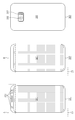
도 3은 다양한 실시 예에 따른 전자 장치의 외관을 나타낸다. Figure 3 shows the appearance of an electronic device according to various embodiments.
도 3을 참조하면, 다양한 실시 예에 따른 전자 장치들(301 - 303)이 도시되어 있다. 도 3에는 전자 장치(301, 302)의 전면 및 전자 장치(303)의 후면이 도시되어 있다. Referring to FIG. 3, electronic devices 301-303 in accordance with various embodiments are shown. 3 shows a front view of the
일 실시 예에 따르면, 전자 장치(301)의 전면에는 디스플레이(311)가 배치될 수 있다. 상기 디스플레이(311)는 전자 장치(301)의 전면 대부분을 점유할 수 있다. 상기 전자 장치(301)의 전면 상단 영역 A에는 다양한 하드웨어 구성(component)(예: 전면 카메라, 근접 센서, 홍채 센서, 리시버 등)이 배치될 수 있다. 다양한 실시 예에 따르면, 디스플레이(311)는 일부 상기 디스플레이(311)의 종횡비(aspect ratio)는 16:9 또는 18:9일 수 있다. According to one embodiment, a
일 실시 예에 따르면, 전자 장치(302)의 전면에도 디스플레이(321)가 배치될 수 있다. 상기 전자 장치(302)의 전면 상단 영역 B에는 하드웨어 구성이 직접적으로 노출되지 않을 수 있다. 예컨대, 리시버는, 전자 장치(302)의 상단 측면에 배치될 수 있다. 또 다른 예를 들어, 전면 카메라, 근접 센서, 홍채 센서 등은 상기 전면 상단 영역 B 밑(즉, 전면 상단 영역 B의 내부)에 배치될 수 있으며, 커버 글래스에 대한 일정한 처리에 의해 직접적으로 노출되지 않을 수도 있다.According to one embodiment, a
일 실시 예에 따르면, 전자 장치(301, 302)의 디스플레이(311, 312)는, 적어도 하나의 코너가 둥근 디스플레이 패널을 포함할 수 있다. 일 예를 들어, 전자 장치(301, 302)의 좌측 하단(lower-left) 코너 영역 C1, C2 에는 좌측 하단의 코너가 둥글게 형성된 디스플레이 패널이 포함될 수 있다. 상기 좌측 하단의 코너가 둥글게 형성된 디스플레이 패널은, 예를 들어, 후술하는 도 8a 및 도 8b와 같이 구현될 수 있다. According to one embodiment, the
일 실시 예에 따르면, 전자 장치(303)의 후면은 후면 커버(331), 카메라(332), 및 하드웨어 구성(333)이 배치될 수 있다. 상기 후면 커버(331)는 예를 들어, 금속, 유리, 플라스틱, 또는 이들의 조합으로 이루어질 수 있다. 상기 하드웨어 구성(333)은, 예를 들어, 플래시, 생체 센서(예: 심박 센서 등), 자외선 센서 등 다양한 모듈들을 포함할 수 있다. According to one embodiment, the back surface of the
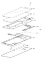
도 4는 일 실시 예에 따른 전자 장치의 분해 사시도를 나타낸다.4 shows an exploded perspective view of an electronic device according to one embodiment.
도 4를 참조하면, 일 실시 예에 따른 전자 장치(401)는 커버 글래스(410), 디스플레이(420), 전면 하드웨어 모듈(425), 브래킷(430), 회로기판(440), 후면 하우징(rear housing)(450), 배터리(460), 및 후면 커버(back cover)(470)를 포함할 수 있다. 다양한 실시 예에 따르면, 전자 장치(401)는 도 4에 도시된 일부 구성을 포함하지 않을 수도 있고, 도 4에 도시되지 않은 구성을 추가로 포함할 수도 있다. 4, an
커버 글래스(410)는 디스플레이(410)에 의해 생성된 빛을 투과시킬 수 있다. 또한, 상기 커버 글래스(410) 상에서 사용자는 신체의 일부(예: 손가락)를 접촉하여 터치(전자 펜을 이용한 접촉을 포함함) 및/또는 지문 인증을 수행할 수 있다. 상기 커버 글래스(410)는, 예컨대, 강화 유리, 강화 플라스틱, 고분자 소재 등으로 형성되어, 디스플레이(420) 및 상기 전자 장치(401)에 포함된 각 구성을 외부 충격으로부터 보호할 수 있다. 다양한 실시 예에 따르면, 상기 커버 글래스(410)는 글래스 윈도우(glass window)로도 참조될 수 있다. The
일 실시 예에 따르면, 커버 글래스(410)의 일측 또는 양측은 휘어질 수 있다. 또한, 일 실시 예에 따르면, 커버 글래스(410)의 둘레 중 적어도 하나의 코너는 둥글게 형성될 수 있다. 도 4에 도시된 커버 글래스(410)의 경우 하단에 배치된 2개의 코너들이 둥글게 형성되어 있으나, 이에 제한되지 않는다. 예컨대, 커버 글래스(410)의 4개의 코너들은 모두 둥글게 형성될 수도 있다. According to one embodiment, one or both sides of the
디스플레이(420)는 상기 커버 글래스(410) 밑에 배치 또는 결합되어, 상기 커버 글래스(410)의 통해 노출될 수 있다. 상기 디스플레이)(420)는 콘텐트(예: 텍스트, 이미지, 비디오, 아이콘, 위젯, 또는 심볼 등)를 출력하거나, 사용자로부터 터치 입력(터치, 제스처, 호버링(hovering)을 수신할 수 있다. 상기 디스플레이(420)는, 예를 들어, 디스플레이 패널, 터치 패널, 및/또는 지문 센서를 포함할 수 있다. 상기 디스플레이(420)의 배면에는 구리(Cu) 또는 그래파이트(graphite)로 이루어진, 이른바, 백 패널이 배치될 수 있다. 상기 디스플레이(420)의 적층 구조는 도 5에서 보다 상세히 설명된다.The
일 실시 예에 따르면, 디스플레이(420)의 일측 또는 양측은 휘어질 수 있다. 또한, 일 실시 예에 따르면, 디스플레이(420)의 둘레 중 적어도 하나의 코너는 둥글게 형성될 수 있다. 도 4에 도시된 디스플레이(420)의 경우 하단에 배치된 2개의 코너들이 둥글게 형성되어 있으나, 이에 제한되지 않는다. 예컨대, 디스플레이(420)의 4개의 코너들은 모두 둥글게 형성될 수도 있다. According to one embodiment, one or both sides of the
일 실시 예에 따르면, 상기 디스플레이(420)의 디스플레이 패널은 LCD 패널, LED 디스플레이 패널, OLED 디스플레이 패널, 또는 MEMS 디스플레이 패널, 또는 전자 종이 디스플레이 패널을 포함할 수 있다. 또한 예를 들어, 상기 디스플레이(420)에 포함되는 터치 패널은 정전식 터치 패널, 감압식 터치 패널, 저항식 터치 패널, 또는 적외선 터치 패널을 포함할 수 있다.According to one embodiment, the display panel of the
전면 하드웨어 모듈(425)은 전면 카메라, 근접 센서, 홍채 센서, 리시버, 지문 센서 등 다양한 구성을 포함할 수 있다. 상기 전면 하드웨어 모듈(425)은 커버 글래스(410) 밑에 배치되어 외부에 노출될 수 있다. 다양한 실시 예에 따르면, 상기 전면 하드웨어 모듈(425)은 디스플레이(420) 밑에 배치되어 외부에 노출되지 않을 수도 있다. The
브래킷(bracket)(430)은 예를 들어, 마그네슘 합금으로 구성되어, 디스플레이(420)의 아래, 및 회로기판(440) 위에 배치될 수 있다. 상기 브래킷(430)은 상기 디스플레이(420) 및 상기 회로기판(440)과 결합되어 이들을 물리적으로 지지할 수 있다. 일 실시 예에 따르면, 상기 브래킷(430)에는 경년 변화에 따른 배터리(460)의 부풀어오름을 감안한 스웰링 갭(swelling gap)이 형성되어 있을 수 있다. The
회로기판(440)은 예를 들어, 메인(main) 회로기판(440m), 및 서브(sub) 회로기판(440s)을 포함할 수 있다. 일 실시 예에 따르면, 상기 메인 회로기판(440m)과 상기 서브 회로기판(440s)은 브래킷(430) 밑에(below) 배치되고(disposed), 이들은 커넥터 또는 배선을 통해 서로 전기적으로 연결될 수 있다. 상기 회로기판들(440m, 440s)은, 예를 들어, 경성 인쇄 회로기판(rigid PCB; rigid printed circuit board)으로 구현될 수 있다. 상기 회로기판(440m, 440s)은 메인보드, PBA(printed board assembly)또는, 단순히 PCB로 참조될 수 있다. 상기 회로기판들(440m, 440s)에는 전자 장치(401)의 각종 전자 부품(예: 프로세서, 메모리, 등), 소자, 인쇄회로 등이 실장(mount) 또는 배치(arrange)될 수 있다. The
(후면) 하우징(450)은 회로기판(440) 밑에 배치되어, 상기 전자 장치(401)의 각 구성을 수납할 수 있다. 상기 하우징(450)은 전자 장치(401)의 측면 외관을 형성할 수 있다. 다양한 실시 예에 따르면, 상기 하우징(450)은 후면 케이스(rear case), 또는 리어 플레이트(rear plate) 등으로도 참조될 수 있다. (Rear View) The
배터리(460)는 화학 에너지와 전기 에너지를 상호 변환할 수 있다. 예를 들어, 배터리(460)는 화학 에너지를 전기 에너지로 변환하여, 상기 전기 에너지를 디스플레이(420) 및 회로기판(440)에 탑재된 다양한 구성 또는 모듈에 공급할 수 있다. 상기 배터리(460)는 외부로부터 공급받은 전기 에너지를 화학 에너지로 변환하여 저장할 수도 있다. 이를 위해, 회로기판(440)에는 배터리(460)의 충방전을 관리하기 위한 전력 관리 모듈이 포함될 수 있다. The
후면 커버(470)는 전자 장치(401)의 후면에 결합될 수 있다. 상기 후면 커버(470)는, 강화유리, 플라스틱 사출물, 및/또는 금속 등으로 형성될 수 있다. 다양한 실시 예에 따르면, 후면 커버(470)는 상기 후면 하우징(450)과 일체로 구현되거나, 또는 사용자에 의해 착탈 가능(detachable)하도록 구현될 수도 있다.The
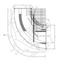
도 5는 일 실시 예에 따른 전자 장치의 측면 단면도 및 디스플레이의 적층 구조를 나타낸다.5 shows a side cross-sectional view of an electronic device according to one embodiment and a stacked structure of a display.
도 5를 참조하면, 일 실시 예에 따른 전자 장치(501)의 우측면 단면도가 도시되어 있다. 상기 우측면 단면도에 따르면, 전자 장치(501)는 글래스 윈도우(510), 디스플레이(520), 테이프(530), 브래킷(540), 하우징(550), 및 후면 커버(560)를 포함할 수 있다. Referring to Fig. 5, a right side cross-sectional view of an
일 실시 예에 따르면, 글래스 윈도우(510) 밑에는 디스플레이(520)가 배치될 수 있고, 상기 디스플레이(520)는 테이프(530)를 개재하여 브래킷(540)과 부착될 수 있다. 도 5에 도시된 바와 같이, 상기 글래스 윈도우(510)와 상기 디스플레이(520)는 브래킷(540)의 형상에 따라서 굽어질(bended) 수 있다. 상기 브래킷(540)은 하우징(550)과 결합될 수 있으며, 상기 하우징(550)은 후면 커버(560)와 결합될 수 있다. According to one embodiment, a
일 실시 예에 따르면, 디스플레이(520)는, 편광층(polarizer)(521), 터치 스크린 패널(터치 센서)(522), 및 디스플레이 패널(523)을 포함할 수 있다. 상기 디스플레이(520)는 OCA(optical clear adhesive) 필름(515)을 개재하여 글래스 윈도우(510)와 결합할 수 있으며, 상기 글래스 윈도우(510)의 일 측은 하우징(550)에 접할 수 있다. According to one embodiment, the
편광층(또는, 편광 필름)(521)은 야외 시인성을 향상시키기 위해 지정된 방향으로 편광된 빛을 통과시킬 수 있다. 상기 편광층(521)은 PET(poly ethylene terephthalate) 필름 또는 TAC(tri-acetyl cellulose) 필름으로 구성될 수 있다. The polarizing layer (or polarizing film) 521 can pass the polarized light in the designated direction to improve outdoor visibility. The
터치 스크린 패널(터치 센서)(522)에서는 사용자의 터치에 의해 변화하는 물리량(예: 정전용량)이 변화할 수 있다. 상기 물리량의 변화는 터치 IC 등을 통해 프로세서에 제공될 수 있으며, 상기 물리량의 변화에 기반하여 상기 사용자의 터치가 이루어진 위치가 파악될 수 있다. In the touch screen panel (touch sensor) 522, a physical quantity (for example, electrostatic capacity) that changes due to a user's touch may change. The change of the physical quantity may be provided to the processor through a touch IC or the like, and the position of the user's touch may be grasped based on the change of the physical quantity.
디스플레이 패널(523)은, 예를 들어, 디스플레이 구동 회로(DDI; display driver IC)로부터 스캔 라인(scan line) 및 데이터 라인(data line)을 통해 공급되는 신호들에 기반하여 빛을 생성할 수 있다. 상기 디스플레이 패널(523)의 일례로서 OLED 패널은, 유기 발광 소자, 상기 발광 소자가 배치되는 기판(예: 저온 폴리실리콘(LTPS: low temperature poly silicon) 기판), 상기 발광 소자를 보호하기 위한 박막 봉지 필름(TFE: thin film encapsulation)을 포함할 수 있다. The
도 5에서 터치 스크린 패널(522)은 별도 구성으로 도시되어 있으나, 다양한 실시 예에 따르면, 상기 터치 스크린 패널(522)은 디스플레이 패널(523)과 일체로 구현될 수 있다(in-cell touch panel). 이 경우, 예컨대, 상기 터치 스크린 패널(522)은 디스플레이 패널(523)의 박막 봉지 필름(TFE)에 형성될 수 있다. 5, the
도 6은 일 실시 예에 따른 전자 장치의 전면 상단을 나타낸다. 6 shows a top front view of an electronic device according to one embodiment.
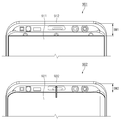
도 6을 참조하면, 일 실시 예에 따른 전자 장치(610)는 디스플레이 패널(610)(예: 도 5의 디스플레이 패널(523)), 커버 글래스(620)(예: 도 5의 글래스 윈도우(510)), 및 하우징(630) (예: 도 5의 하우징(550))을 포함할 수 있다. 상기 하우징(630) 은 디스플레이 패널(610)을 수납할 수 있고, 커버 글래스(620)와 결합할 수 있다. 상기 커버 글래스(620)는 디스플레이 패널(610) 위에 배치될 수 있다. 6, an
일 실시 예에 따르면, 디스플레이 패널(610), 커버 글래스(620), 및 하우징(630) 각각의 외관 윤곽(contour)은 4개의 코너들이 곡선으로 이루어진 둥근 사각형(rounded rectangle) 형상을 가질 수 있다. According to one embodiment, the contour of each of the
일 실시 예에 따르면, 디스플레이 패널(610)은 활성 영역(active area)(610a), 및 상기 활성 영역(610a)을 둘러싼 비활성 영역(inactive area)(610i)을 포함할 수 있다. 상기 활성 영역(610a)에는, 예컨대, OLED를 포함한 복수의 화소들이 배치될 수 있다. 상기 활성 영역(610a)의 둘레 중 적어도 하나(예: 2개 또는 4개)의 코너는 곡선으로 형성될 수 있다. 상기 비활성 영역(610i)에는 상기 복수의 화소들이 배치되지 아니하며, 일정한 회로 구성(예: 에미션 드라이버, 게이트 드라이버 등), 또는 다양한 신호(예: ELVSS 전압, ELVDD 전압, Data 신호, Scan 신호, EM 신호 등) 등이 전달되는 배선이 형성될 수 있다. According to one embodiment, the
일 실시 예에 따르면, 활성 영역(610a)의 둘레(circumference) 및 비활성 영역(610i)의 외측 둘레(즉, 디스플레이 패널(610)의 윤곽)은, 적어도 하나의 코너가 곡선으로 이루어진 둥근 사각형 형상을 가질 수 있다. According to one embodiment, the circumference of the
예를 들어, 상기 활성 영역(610a)의 둘레는 제1 방향(예: 세로 방향)으로 연장된 세로변(vertical periphery 또는 vertical side) Va, 상기 제1 방향에 수직인 제2 방향(예: 가로 방향)으로 연장된 가로변(horizontal periphery 또는 horizontal side) Ha, 및 상기 세로변 및 가로변을 연결하는 곡선 Ra을 포함할 수 있다. 또한, 예를 들어, 비활성 영역(610i)의 외측 둘레(즉, 디스플레이 패널(610)의 윤곽)은 상기 제1 방향으로 연장된 세로변 Vb, 상기 제2 방향으로 연장된 가로변 Hb, 및 상기 세로변 Vb 및 가로변 Hb을 연결하는 곡선 Rb를 포함할 수 있다. For example, the perimeter of the
일 실시 예에 따르면, 활성 영역(610a)에 있어서, 세로변 Va와 곡선 Ra가 접하는 경계 지점에서부터, 곡선 Ra와 가로변 Ha가 접하는 경계 지점까지 이르는 동안, 상기 곡선 Ra의 곡률 반경은 점진적으로(gradually) 작아질 수 있다. 유사하게, 비활성 영역(610i)의 외측 둘레(즉, 디스플레이 패널(610)의 윤곽)에 있어서, 세로변 Vb와 곡선 Rb가 접하는 경계 지점에서부터, 곡선 Rb와 가로변 Hb가 접하는 경계 지점까지 이르는 동안, 상기 곡선 Rb의 곡률 반경은 점진적으로 작아질 수 있다.According to one embodiment, in the
일 실시 예에 따르면, 비활성 영역(610i)의 외측 둘레(즉, 디스플레이 패널(610)의 윤곽) 중 어느 한 코너를 이루는 곡선의 평균 곡률 반경(average radius of curvature)은, 활성 영역(610a)의 둘레 중 어느 한 코너를 이루는 곡선의 평균 곡률 반경보다 크게 설계될 수 있다. 예를 들어, 비활성 영역(610i)의 외측 둘레(즉, 디스플레이 패널(610)의 윤곽) 중 우측 상단 코너를 이루는 곡선 Rb의 평균 곡률 반경은 활성 영역(610a)의 둘레 중 우측 상단 코너를 이루는 곡선 Ra의 평균 곡률 반경보다 클 수 있다. According to one embodiment, the average radius of curvature of a curve that forms a corner of the outer perimeter of the
일 실시 예에 따르면, 비활성 영역(610i)의 외측 둘레(즉, 디스플레이 패널(610)의 윤곽) 중 어느 한 코너를 이루는 곡선의 길이는, 활성 영역(610a)의 둘레 중 어느 한 코너를 이루는 곡선의 길이보다 길게 설계될 수 있다. 예컨대, 비활성 영역(610i)의 외측 둘레(즉, 디스플레이 패널(610)의 윤곽) 중 우측 상단 코너를 이루는 곡선 Rb의 길이는 활성 영역(610a)의 둘레 중 우측 상단 코너를 이루는 곡선 Ra의 길이보다 길 수 있다.According to one embodiment, the length of the curve that forms one of the corners of the outer periphery of the
커버 글래스(620)는 둥근 사각형 형상을 가지되, 상기 커버 글래스(620)의 윤곽은 제1 방향으로 연장된 세로변 Vc, 제2 방향으로 연장된 가로변 Hc, 및 상기 세로변 Vc 및 가로변 Hc를 연결하는 곡선 Rc를 포함할 수 있다. 이때, 세로변 Vc과 곡선 Rc가 접하는 경계 지점에서부터, 곡선 Rc와 가로변 Hc가 접하는 경계 지점까지 이르는 동안, 상기 곡선 Rc의 곡률 반경은 점진적으로(gradually) 작아질 수 있다. The
일 실시 예에 따르면, 커버 글래스(620)의 윤곽 중 어느 한 코너를 이루는 곡선의 평균 곡률 반경은, 비활성 영역(610i)의 외측 둘레(즉, 디스플레이 패널(610)의 윤곽) 중 어느 한 코너를 이루는 곡선의 평균 곡률 반경보다 크게 설계될 수 있다. 예를 들어, 커버 글래스(620)의 윤곽 중 우측 상단 코너를 이루는 곡선 Rc의 평균 곡률 반경은, 디스플레이 패널(610)의 윤곽 중 우측 상단 코너를 이루는 곡선 Rb의 평균 곡률 반경보다 클 수 있다.According to one embodiment, the average curvature radius of the curved line constituting one of the contours of the
하우징(630)은 둥근 사각형 형상을 가지되, 상기 하우징(630)의 윤곽은 제1 방향으로 연장된 세로변 Vd, 제2 방향으로 연장된 가로변 Hd, 및 상기 세로변 Vd 및 가로변 Hd를 연결하는 곡선 Rd를 포함할 수 있다. 이때, 세로변 Vd와 곡선 Rd가 접하는 경계 지점에서부터, 곡선 Rd와 가로변 Hd가 접하는 경계 지점까지 이르는 동안, 상기 곡선 Rd의 곡률 반경은 점진적으로 작아질 수 있다.The
일 실시 예에 따르면, 하우징(630)의 윤곽 중 어느 한 코너를 이루는 곡선의 평균 곡률 반경은, 커버 글래스(620)의 윤곽 중 어느 한 코너를 이루는 곡선의 평균 곡률 반경보다 크게 설계될 수 있다. 예를 들어, 하우징(630)의 윤곽 중 우측 상단 코너를 이루는 곡선 Rd의 평균 곡률 반경은, 커버 글래스(620)의 윤곽 중 우측 상단 코너를 이루는 곡선 Rc의 평균 곡률 반경보다 클 수 있다. According to one embodiment, the average curvature radius of a curve forming one of the contours of the
다양한 실시 예에 따르면, 상기 디스플레이 패널(610)은
도 4 및 도 5에 도시된 바와 같이, 전면 및 적어도 하나의 측면을 포함할 수 있다. 상기 디스플레이 패널(610)에 형성된 비활성 영역(610i)의 적어도 일부는, 상기 적어도 하나의 측면에 배치될 수 있다. 이 경우, 상기 디스플레이 패널(610)을 구동하기 위한 디스플레이 구동 회로는 상기 적어도 하나의 측면에 배치될 수 있다. According to various embodiments, the
도 7은 일 실시 예에 따른 전자 장치 블록도를 나타낸다. 7 shows an electronic device block diagram according to one embodiment.
도 7을 참조하면 일 실시 예에 따른 전자 장치는, 프로세서(710), 디스플레이 구동 회로(DDI)(720), 디스플레이 패널(730), 및 화소 전원(740)을 포함할 수 있다. 다양한 실시 예에 따르면, 상기 화소 전원(740)은 디스플레이 구동 회로(DDI)(720)에 포함될 수 있다. 7, an electronic device according to an embodiment may include a
프로세서(710)(호스트(host))는 메모리 또는 네트워크로부터 영상 데이터를 획득하고, 상기 획득된 영상 데이터를 디스플레이 구동 회로(720)에 제공할 수 있다. The processor 710 (host) may acquire image data from a memory or a network, and may provide the acquired image data to the
디스플레이 구동 회로(720)는 상기 프로세서(710)로부터 수신한 영상 데이터에 대응하는 신호 및 전력를 생성하여 디스플레이 패널(730)에 공급할 수 있다. The
일 실시 예에 따르면, 상기 디스플레이 구동 회로(720)는 프레임 버퍼(721), 이미지 프로세싱 유닛(IP; image processing unit)(722), 게이트 드라이버(723), 소스 드라이버(724), 및 타이밍 컨트롤러(T-CON; timing controller)(725)를 포함할 수 있다. 다양한 실시 예에 따르면, 디스플레이 구동 회로(720)는 오실레이터(oscillator), 프레임율(frame rate) 조절 모듈 등을 더 포함할 수 있다.According to one embodiment, the
프레임 버퍼(721)는 프로세서(710)(호스트)로부터 수신된 영상 데이터를 저장할 수 있다. 일 실시 예에 따르면, 상기 프레임 버퍼(721)는 상기 영상 데이터의 해상도(resolution) 및 색 계조수(色階調數; number of color gradations)에 대응하는 메모리 공간을 포함할 수 있다. 다양한 실시 예에 따르면, 상기 프레임 버퍼(721)는 그래픽 램(graphic RAM) 또는 라인 버퍼(line buffer)로 참조될 수 있다.The
이미지 프로세싱 유닛(IP)(722)은 상기 프레임 버퍼(721)로부터 제공된 영상 데이터의 화질을 개선 또는 보정할 수 있다. 예컨대, 상기 이미지 프로세싱 유닛(IP)(722)은 화소 어레이(731)의 화소 배치 구조(pixel layout)에 따라서, 영상 데이터를 보정할 수 있다.The image processing unit (IP) 722 may improve or correct the image quality of the image data provided from the
게이트 드라이버(723) 및 소스 드라이버(724)는 타이밍 컨트롤러(725)의 제어 하에 디스플레이 패널(730)에 공급하는 신호(71, 72)를 생성할 수 있다. The
게이트 드라이버(723)는 스캔 라인(scan line)을 통해 스캔 신호(71) (또는, 게이트 신호)를 디스플레이 패널(730)의 각 화소에 공급할 수 있다. 상기 게이트 드라이버(723)는 상기 스캔 신호(71)에 기반하여 스캔 트랜지스터(scan TFT)의 게이트 단의 전압을 제어할 수 있으며, 이를 통해 각 화소의 발광 여부를 제어할 수 있다. 상기 게이트 드라이버(723)는 디스플레이 패널(730)의 좌측에 배치된 것으로 도시되어 있으나, 이는 개념도로서 도시된 예에 제한되지 않는다. 예컨대, 상기 게이트 드라이버(723)는 스캔 신호(71)의 전압 강하(voltage drop)를 방지하기 위해 디스플레이 패널(730)의 양측으로부터 상기 스캔 신호(71)를 공급할 수도 있다.The
소스 드라이버(724)는 데이터 라인(data line)을 통해 데이터 신호(또는, 소스 신호)(72)를 디스플레이 패널(730)의 각 화소에 공급할 수 있다. 상기 소스 드라이버(724)는 상기 데이터 신호(72)를 인가하여 각 화소들의 발광 세기를 제어할 수 있다.The
타이밍 컨트롤러(T-CON)(725)는 게이트 드라이버(723) 및 소스 드라이버(724)에 영상 데이터에 대응하는 영상 신호를 제공할 수 있다. 상기 타이밍 컨트롤러(T-CON)(725)는 게이트 드라이버(723) 및 소스 드라이버(724)로부터 송출되는 신호의 송출 타이밍을 제어할 수 있다. The timing controller (T-CON) 725 can provide the video signal corresponding to the video data to the
디스플레이 패널(730)은 화소 어레이(pixel array)(731), 에미션 드라이버(emission driver)(732), 및 ESD(electrostatic discharge) 보호 회로(733)를 포함할 수 있다. 상기 화소 어레이(731)는 디스플레이 패널(730)의 활성 영역을 구성할 수 있으며, 둥근 사각형 형상을 가질 수 있다. 예컨대, 화소 어레이(731)에 포함된 화소들의 배치 구조(layout)에 따라서 상기 화소 어레이(731)는 둥근 사각형 형상을 가질 수 있다. 상기 에미션 드라이버(732) 및 ESD 보호 회로(733)는 디스플레이 패널(730)의 비활성 영역에 배치 또는 형성될 수 있다. The
화소 어레이(731)는 다수(예: 수백만개)의 화소들을 포함할 수 있다. 상기 화소 어레이(731)로부터 발생하는 빛에 기초하여 콘텐츠(예: 이미지, 텍스트, 비디오 등)이 출력될 수 있다. 예를 들어, 화소(735)를 비롯한 각 화소는 적색(red) 필터, 녹색(green) 필터, 및 청색(blue) 필터를 구비한 서브 화소(sub-pixel)를 포함할 수 있다. The
에미션 드라이버(732)는 각 화소에 발광 제어 신호(이하, EM 신호)(73)를 인가함으로써, 화소의 발광 타이밍을 제어할 수 있다. 일 실시 예에 따르면 에미션 드라이버(732)는 복수 개의 블록으로 분리될 수 있다. 분리된 블록 각각은 "에미션 구동 블록(emission driving block)" 혹은 "EM 블록"으로 참조될 수 있다. 다양한 실시 예에 따르면, 도 7에 도시된 것과는 달리, 상기 에미션 드라이버(732)는 디스플레이 구동 회로(720) 내에 포함되어 구현될 수도 있다.The
ESD 보호 회로(733)는 전자 장치 내부 또는 외부에서 유래한 정전기를 차단할 수 있다. The
화소 전원(pixel power source)(740)은 화소 어레이(731)에 포함된 화소들에 전기적으로 연결되어, 각 화소가 빛을 생성할 수 있도록 전원을 공급할 수 있다. 일 실시 예에 따르면, 화소 전원(740)은 DC/DC 컨버터를 포함할 수 있으며, 상기 화소 전원(740)는 DC/DC 컨버터에 의해 변환된 전압, 예컨대, 제1 전압(예: ELVDD)(74)과 제2 전압(예: ELVSS)(75)을 화소들에 인가할 수 있다. 상기 The
일 실시 예에 따르면, 상기 디스플레이 패널(730)은 OLED 패널일 수 있다. 이에 따라, 상기 디스플레이 패널(730)에 포함된 하나의 화소(735)에는 OLED, 수 개의 트랜지스터, 및 커패시터가 배치될 수 있다. 일 실시 예에 따르면, 게이트 드라이버(723)로부터 수신된 스캔 신호(SCAN)(71)에 기반하여 화소(735)의 발광 여부가 결정될 수 있고, 소스 드라이버(724)로부터 수신된 데이터 신호(DATA)(72)에 기반하여 화소(735)의 발광 세기가 결정될 수 있다. 또한, 화소 전원(740)로부터 인가된 전압(ELVDD(74), ELVSS(75))에 의해 화소(735)에 포함된 OLED가 발광할 수 있다. 상기 에미션 드라이버(732)로부터 수신된 EM 신호(73)에 의해 화소(735)에 포함된 OLED의 발광 타이밍이 제어될 수 있다. According to one embodiment, the
도 8a는 일 실시 예에 따른 전자 장치의 좌측 하단 영역을 나타낸다. 8A shows a left lower region of an electronic device according to one embodiment.
도 8a를 참조하면, 일 실시 예에 따른 전자 장치(801)의 좌측 하단 영역이 도시되어 있다. 상기 전자 장치(801)은 디스플레이 패널(810), 커버 글래스(820), 및 하우징(830)을 포함할 수 있다. Referring to FIG. 8A, a left bottom region of an
일 실시 예에 따르면, 상기 디스플레이 패널(810)은 곡선 Ra를 경계로 활성 영역(810a) 및 비활성 영역(810i)으로 구분될 수 있다. According to one embodiment, the
상기 활성 영역(810a)에는 다수의 화소가 배치될 수 있다. 예컨대, 활성 영역(810a)의 적어도 하나의 코너에 있어서, 상기 다수의 화소(예: 도 7의 화소(735))는 곡선 Ra를 따라서 배치될 수 있다. 상기 곡선 Ra는 상기 다수의 화소를 배치하기 위한 기준선을 의미할 수 있다. 화소의 크기(pitch)는 마이크로미터 또는 나노미터 스케일을 가지므로, 도 8a에 도시된 곡선 Ra는 실질적으로 상기 다수의 화소의 둘레를 나타내는 것으로 이해될 수 있다. 다양한 실시 예에 따르면, 도 8a에서는 곡선 Ra가 일례로 도시되어 있으나, 이에 제한되지 않는다. 예를 들어, 상기 곡선 Ra는 직선 선분 및/또는 곡선 선분이 조합된 굴절선(refraction line)으로 구현될 수도 있다. A plurality of pixels may be disposed in the
상기 비활성 영역(810i)에는 디스플레이 구동 회로가 다수의 화소에 신호 또는 전력을 공급하기 위한 회로, 소자, 모듈, 또는 전기적 경로가 다수의 층을 이루며 형성될 수 있다. In the
예를 들어, 디스플레이 구동 회로의 소스 드라이버로부터 인출된 전기적 경로들(811)은, 게이트 드라이버 (예: 도 7의 723) 및/또는 에미션 드라이버(예: 도 7의 732)로부터 인출된 전기적 경로들(812)과, 비활성 영역(810i)의 코너 영역(80B) 중 일부 영역(80A)에서 꼬인 위치(skew position)로 교차할 수 있다. 즉, 데이터 신호의 전달 경로(811)와 스캔 신호 및/또는 EM 신호의 전달 경로(812)는 코너 영역(80B) 중 일부 영역(80A)에서 꼬인 위치로 교차할 수 있다. 전기적 경로들(811, 812)이 서로 꼬인 위치로 교차한다고 함은, 전기적 경로(811)와 전기적 경로(812)가 서로 교차하되, 신호 전달에 있어서 상호 영향을 미치지 않는 것(즉, 전기적 경로들(811, 812)이 전기적으로 연결되지 않는 것)을 의미할 수 있다. For example, the
일 실시 예에 따르면, 도 6과 유사하게, 비활성 영역(810i)의 외측 둘레 중 곡선 Rb의 평균 곡률 반경은 활성 영역(610a)의 둘레 중 곡선 Ra의 평균 곡률 반경보다 클 수 있다. 또한, 일 실시 예에 따르면, 상기 곡선 Ra 및 곡선 Rb의 곡률 반경은 각각의 세로변과의 경계에서 가로변과의 경계에 이르는 동안 점진적으로 작아질 수 있다.6, the average radius of curvature of the curve Rb in the outer periphery of the
일 실시 예에 따르면, 상기 코너 영역(80B)은, (i) 곡선 Ra (P1-P2); (ii) 활성 영역(810a)의 세로변과 곡선 Ra가 접하는 지점 P1에서부터 비활성 영역(810i)의 외측 세로변(즉, 디스플레이 패널(810)의 세로변)과 곡선 Rb가 접하는 지점 P3까지 연결한 가상의 선 (P1-P3); (iii) 곡선 Rb (P3-P4); (iv) 활성 영역(810a)의 가로변과 곡선 Ra가 접하는 지점 P2에서부터 비활성 영역(810i)의 외측 가로변(즉, 디스플레이 패널(810)의 가로변)과 곡선 Rb가 접하는 지점 P4까지 연결한 가상의 선(P2-P4);에 의해 둘러싸인 영역에 해당할 수 있다. According to one embodiment, the corner region (80B) is, (i) the curve Ra (P 1 -P 2); (ii) the outer longitudinal sides of the active region (810a), longitudinal sides and curved non-active area (810i) from the point P 1 Ra is in contact with (that is, a portrait on the
또한, 일 실시 예에 따르면, 코너 영역(80B) 중 일부(80A)영역은, (i) 곡선 Ra; (ii) 활성 영역(810a)의 세로변을 하단 방향으로 연장한 가상의 선; (iii) 활성 영역(810a)의 가로변을 좌측 방향으로 연장한 가상의 선;에 의해 둘러싸인 영역에 해당할 수 있다. Also, according to one embodiment, a
다양한 실시 예에 따르면, 상기 비활성 영역(810i)에는 기타 다양한 회로 구성, 회로, 소자, 모듈, 또는 전기적 경로 등이 형성 또는 배치될 수 있다. 예를 들어, 도 8a의 실시 예에 따르면, 화소 전원(예: 도 7의 740)으로부터 인출된 제1 배선(ELVDD 인가 배선)(813); 게이트 드라이버 (예: 도 7의 723), 에미션 드라이버(예: 도 7의 732), 게이트 드라이버 및/또는 에미션 드라이버로부터 인출된 전기적 경로를 포함하는 블록들(814); ESD 소자를 포함한 기타 회로 구성(815); ESD 보호 회로(816); 및 화소 전원으로부터 인출된 제2 배선(ELVSS 인가 배선)(817)은, 비활성 영역(810i)에 형성 또는 배치될 수 있다. 상기 각 구성들(813-817)의 배치 관계는, 예를 들어, 이하와 같이 설명될 수 있다. According to various embodiments, various other circuit configurations, circuits, elements, modules, or electrical paths may be formed or disposed in the
일 실시 예에 따르면, 화소 전원으로부터 인출된 상기 제1 배선(ELVDD 인가 배선)(813) 및 상기 제2 배선(ELVSS 인가 배선)(817)은, 활성 영역(810a)의 적어도 일부를 둘러싸도록 배치될 수 있다. According to one embodiment, the first wiring (ELVDD applied wiring) 813 and the second wiring (ELVSS applied wiring) 817 drawn out from the pixel power supply are arranged so as to surround at least a part of the
일 실시 예에 따르면, 게이트 드라이버 및/또는 에미션 드라이버로부터 인출된 전기적 경로(812)의 일부와 소스 드라이버로부터 인출된 전기적 경로(811)의 일부는, 곡선 Ra와 상기 제1 배선(ELVDD 인가 배선)(813) 사이 공간에서 교차할 수 있다. According to one embodiment, a part of the
일 실시 예에 따르면, 제1 배선(ELVDD 인가 배선)(813)의 일부는, 곡선 Ra와 게이트 드라이버 및/또는 에미션 드라이버로부터 인출된 전기적 경로(812) 사이에 배치될 수 있다. 또한, 게이트 드라이버 및/또는 상기 에미션 드라이버로부터 인출된 전기적 경로의 일부(812)는, 상기 제1 배선(ELVDD 인가 배선)(813)의 일부, 및 상기 제2 배선(ELVSS 인가 배선)(817)의 사이에 배치될 수 있다. 한편, ESD 보호 회로(816)는 제1 배선(ELVDD 인가 배선)(813) 및 제2 배선(ELVSS 인가 배선)(817) 사이에 배치될 수 있다. According to one embodiment, a portion of the first wiring (ELVDD applied wiring) 813 may be disposed between the curved line Ra and the
요컨대, 도 8b의 가상의 선 A-A'를 참조하면(도 8a의 복잡성을 완화하기 위해 도 8b에 도시함), 상기 가상의 선 A-A'을 따라서(along with) 활성 영역(810a)에 포함된 화소들; 게이트 드라이버, 소스 드라이버, 및/또는 에미션 드라이버로부터 인출된 전기적 경로들(811, 812)의 일부; 제1 배선(ELVDD 인가 배선)(813); 게이트 드라이버, 소스 드라이버, 및/또는 에미션 드라이버로부터 인출된 전기적 경로들(811, 812)의 일부; 게이트 드라이버 및/또는 에미션 드라이버로부터 인출된 전기적 경로를 포함하는 블록들(814); 제2 배선(ELVSS 인가 배선)(817);이 순차로 등장(appear)할 수 있다. 8A). In other words, referring to the imaginary line A-A 'of FIG. 8B (shown in FIG. 8B to alleviate the complexity of FIG. 8A), the
다양한 실시 예에 따르면, 상기 게이트 드라이버, 및/또는 에미션 드라이버는, 예를 들어, 상기 블록들(814)에 포함되거나, 디스플레이 구동 회로 내부에 배치될 수 있다. 또한, 예를 들어, 상기 블록들(814)은, 게이트 드라이버, 및/또는 에미션 드라이버의 일부를 구성할 수있으며, 상기 블록들(814)은 각각 적어도 하나의 트랜지스터를 포함할 수 있다. 일 실시 예에 따르면, 상기 코너 영역(80B) 중 일부(80A)영역에는 상기 블록들(814) 중 적어도 하나가 배치될 수 있다.According to various embodiments, the gate driver and / or the emission driver may be included, for example, in the
도 8a에 도시된 실시 예에 따르면, 곡선 Rb의 평균 곡률 반경은 곡선 Ra의 평균 곡률 반경보다 클 수 있다. 또한, 상기 곡선 Ra 및 Rb의 곡률 반경은 세로변과의 경계에서 가로변의 경계에 이르는 동안 작아질 수 있다. 곡선 Ra와 곡선 Rb 사이의 폭은, 보조선 a(P1-P2)에서 보조선 b(P3-P4)에 이르는 동안, 상기 보조선 a(P1-P2)의 길이 보다 긴 위치가 적어도 하나 존재할 수 있다. 이러한 곡선 Ra 및 곡선 Rb의 형상으로 인해, 도 8에 도시된 보조선 b의 길이는 보조선 a의 길이보다 길어질 수 있다. 이를 통해, 비활성 영역(810i)에는 다양한 회로 구성, 회로, 소자, 모듈, 또는 전기적 경로 등이 배치될 수 있는 공간이 확보될 수 있다. According to the embodiment shown in Fig. 8A, the average radius of curvature of the curve Rb may be larger than the average radius of curvature of the curve Ra. In addition, the radius of curvature of the curves Ra and Rb can be reduced while reaching the boundary of the side of the road at the boundary with the longitudinal side. The width of the curve between the curved lines Ra and Rb is, auxiliary line a (P 1 -P 2) in the auxiliary line b (P 3 -P 4) for a, is longer than the length of the auxiliary line a (P 1 -P 2) ranging from There can be at least one location. Due to the shapes of the curved line Ra and the curved line Rb, the length of the auxiliary line b shown in Fig. 8 can be longer than the length of the auxiliary line a. Thus, the
도 8b는 또 다른 실시 예에 따른 전자 장치의 좌측 하단 영역을 나타낸다. 8B shows a left lower end region of an electronic device according to another embodiment.
도 8b를 참조하면, 일 실시 예에 따른 전자 장치(801)의 좌측 하단 영역이 도시되어 있다. 상기 전자 장치(801)은 디스플레이 패널(810), 커버 글래스(820), 및 하우징(830)을 포함할 수 있다. 도 8b에 도시된 구성 중 도 8a와 동일한 참조부호를 가진 구성은 동일한 구성을 지칭하므로, 이들에 대한 설명은 생략하기로 한다. Referring to FIG. 8B, a left bottom region of the
일 실시 예에 따르면, 비활성 영역(810i)의 외측 둘레, 즉, 디스플레이 패널(810)의 윤곽은, 세로변, 가로변, 및 상기 세로변 및 가로변을 연결하는 굴절선(refraction line) F (P3-P4)을 포함할 수 있다. 상기 굴절선 F는 복수의 선분들(f1 - f6)의 조합으로 구성될 수 있다. 이때, 상기 굴절선 F의 길이, 즉, 상기 복수의 선분들(f1 - f6)의 합은, 활성 영역(810a)의 곡선 Ra보다 길게 설계될 수 있다. According to one embodiment, the outer perimeter of the
다양한 실시 예에 따르면, 상기 굴절선 F는 복수의 선분들(f1 - f6) 중 적어도 하나는, 곡선 선분으로 구현될 수도 있다. 즉, 상기 굴절선 F는 직선 선분과 곡선 선분의 조합으로 구성될 수 있다. According to various embodiments, at least one of the plurality of line segments f 1 -f 6 may be implemented as a curved line segment. That is, the refraction line F may be a combination of a straight line segment and a curved line segment.
본 발명의 다양한 실시 예에 의하면, 디스플레이 패널 및 상기 디스플레이 패널에 포함된 활성 영역은 둥근 (또는 실질적으로 둥근) 사각형으로 형성될 수 있다. 이를 통해, 상기 디스플레이 패널은 마찬가지로 둥근 사각형으로 형성된 하우징의 수납 공간에 여분의 영역 및/또는 공간을 최소화시키면서 배치될 수 있다. According to various embodiments of the present invention, the active area included in the display panel and the display panel may be formed as a round (or substantially rounded) rectangle. Accordingly, the display panel can be disposed while minimizing an extra area and / or space in a housing space of a housing formed of a round square.
예를 들어, 도 9를 참조하면, 일반적인 전자 장치(901) 및 본 발명의 일 실시 예에 따른 전자 장치(902)가 도시되어 있다. 전자 장치(901)에 의하면, 디스플레이 패널(911)이 코너가 직각인 직사각형 형상을 가지므로 하우징(912)에서 디스플레이 패널(911)까지 간격은 BM1에 해당한다. 이에 비하여, 전자 장치(902)에 의하면, 디스플레이 패널(921)의 코너는 둥글게 형성될 수 있다. 디스플레이 패널(921)의 코너에서는 본 발명의 다양한 실시 예에 따른 곡률 반경이 적용됨에 따라서, 하우징(922)에서 디스플레이 패널(921)까지 간격이 BM1보다 작은 BM2로 축소될 수 있다. For example, referring to Fig. 9, a general
이와 같이, 본 발명의 다양한 실시 예에 따르면, 하우징(922)에서 디스플레이 패널(921)까지 간격이 BM2로 축소될 수 있으므로, 전자 장치(902)의 전면에서 디스플레이가 점유하는 면적은 극대화될 수 있으며, 보다 향상된 심미감을 사용자에게 제공할 수 있다. Thus, according to various embodiments of the present invention, since the distance from the
일 실시 예에 따른 전자 장치는, 복수의 화소들이 배치된 활성 영역(active area), 및 상기 복수의 화소들이 배치되지 않은 비활성 영역(inactive area)을 포함한 디스플레이 패널을 포함할 수 있다. 상기 활성 영역의 둘레(circumference) 및 상기 디스플레이 패널의 윤곽(contour)은, 적어도 하나의 코너가 곡선으로 이루어진 둥근 사각형(rounded rectangle) 형상을 가질 수 있다. 상기 디스플레이 패널의 윤곽 중 어느 한 코너를 이루는 곡선의 평균 곡률 반경(average radius of curvature)은, 상기 활성 영역의 둘레 중 어느 한 코너를 이루는 곡선의 평균 곡률 반경보다 클 수 있다. An electronic device according to an embodiment may include a display panel including an active area in which a plurality of pixels are arranged and an inactive area in which the plurality of pixels are not arranged. The circumference of the active area and the contour of the display panel may have a rounded rectangle shape in which at least one corner is a curved line. An average radius of curvature of a curved line constituting a corner of the contour of the display panel may be greater than an average curvature radius of a curved line forming a corner of the active region.
일 실시 예에 따르면, 상기 디스플레이 패널의 윤곽 중 어느 한 코너를 이루는 곡선의 길이는, 상기 활성 영역의 둘레 중 어느 한 코너를 이루는 곡선의 길이보다 길게 설계될 수 있다. According to an embodiment of the present invention, the length of the curved line constituting one of the outlines of the display panel may be designed to be longer than the length of the curved line constituting any one of the corners of the active area.
일 실시 예에 따르면, 상기 전자 장치는 상기 디스플레이 패널 위에 배치되는 커버 글래스를 더 포함할 수 있다. 상기 커버 글래스는, 적어도 하나의 코너가 곡선으로 이루어진 둥근 사각형 형상을 가지고, 상기 커버 글래스의 윤곽 중 어느 한 코너를 이루는 곡선의 평균 곡률 반경은 상기 디스플레이 패널의 윤곽 중 어느 한 코너를 이루는 곡선의 평균 곡률 반경보다 클 수 있다. According to one embodiment, the electronic device may further include a cover glass disposed on the display panel. Wherein the cover glass has a round rectangular shape with at least one corner formed by a curved line and an average curvature radius of a curved line constituting a corner of the outline of the cover glass is an average of curves forming a corner of the display panel May be greater than the radius of curvature.
일 실시 예에 따르면, 상기 커버 글래스의 윤곽은 제1 방향으로 연장된 제1 변, 상기 제1 방향에 수직인 제2 방향으로 연장된 제2 변, 및 상기 제1 변 및 제2 변을 연결하는 곡선을 포함할 수 있다. 상기 제1 변과 상기 곡선이 접하는 지점에서부터 상기 곡선과 상기 제2 변이 접하는 지점까지 이르는 동안, 상기 곡선의 곡률 반경은 점진적으로 작아질 수 있다. According to one embodiment, the outline of the cover glass includes a first side extending in the first direction, a second side extending in the second direction perpendicular to the first direction, and a second side extending in the first direction and the second side . ≪ / RTI > The radius of curvature of the curved line gradually decreases from the point where the first side and the curved line come in contact to the point where the curved line comes into contact with the second side.
일 실시 예에 따르면, 상기 전자 장치는, 상기 디스플레이 패널을 수납하고, 상기 커버 글래스와 결합하는 하우징을 더 포함할 수 있다. 상기 하우징은, 적어도 하나의 코너의 코너가 곡선으로 이루어진 둥근 사각형 형상을 가지고, 상기 하우징의 윤곽 중 어느 한 코너를 이루는 곡선의 평균 곡률 반경은 상기 커버 글래스의 윤곽 중 어느 한 코너를 이루는 곡선의 평균 곡률 반경보다 클 수 있다. According to one embodiment, the electronic device may further include a housing for receiving the display panel and coupling with the cover glass. Wherein the housing has a round rectangular shape in which at least one corner has a curved line and an average curvature radius of a curved line forming a corner of the housing is an average of curves forming a corner of the cover glass May be greater than the radius of curvature.
일 실시 예에 따르면, 상기 디스플레이 패널을 수납하는 하우징;을 더 포함하고, 상기 하우징은, 적어도 하나의 코너가 곡선으로 이루어진 둥근 사각형 형상을 가질 수 있다. 상기 하우징의 윤곽 중 어느 한 코너를 이루는 곡선의 평균 곡률 반경은 상기 디스플레이 패널의 윤곽 중 어느 한 코너를 이루는 곡선의 평균 곡률 반경보다 클 수 있다. According to an embodiment, the display apparatus may further include a housing for housing the display panel, and the housing may have a round rectangular shape including at least one corner. The average curvature radius of a curve forming one of the contours of the housing may be greater than an average curvature radius of a curve forming one of the contours of the display panel.
일 실시 예에 따르면, 상기 하우징의 윤곽은 제1 방향으로 연장된 제1 변, 상기 제1 방향에 수직인 제2 방향으로 연장된 제2 변, 및 상기 제1 변 및 제2 변을 연결하는 곡선을 포함할 수 있다. 상기 제1 변과 상기 곡선이 접하는 지점에서부터 상기 곡선과 상기 제2 변이 접하는 지점까지 이르는 동안, 상기 곡선의 곡률 반경은 점진적으로 작아지다가 커질 수 있다. According to one embodiment, the contour of the housing includes a first side extending in a first direction, a second side extending in a second direction perpendicular to the first direction, and a second side extending in the second direction, ≪ / RTI > curve. The radius of curvature of the curved line may gradually decrease and increase from the point where the curved line contacts the first side to the point where the curved line contacts the second side.
일 실시 예에 따르면, 상기 전자 장치는 상기 디스플레이 패널을 구동하기 위한 디스플레이 구동 회로(DDI)를 더 포함할 수 있다. 상기 비활성 영역에는, 상기 디스플레이 구동 회로가 상기 디스플레이 패널에 신호 또는 전력을 공급하기 위한 전기적 경로가 형성될 수 있다. According to an embodiment, the electronic device may further include a display driving circuit (DDI) for driving the display panel. In the inactive region, an electrical path for supplying a signal or power to the display panel may be formed by the display driving circuit.
일 실시 예에 따르면, 상기 디스플레이 구동 회로는, 게이트 드라이버(gate driver) 및 소스 드라이버(source driver)를 포함할 수 있다. 상기 게이트 드라이버로부터 인출된 전기적 경로 및 상기 소스 드라이버로부터 인출된 전기적 경로는, 상기 비활성 영역 중 코너 영역에서 꼬인 위치(skew position)로 교차할 수 있다. According to an embodiment, the display driving circuit may include a gate driver and a source driver. The electrical path drawn from the gate driver and the electrical path drawn from the source driver may intersect a skew position in a corner region of the inactive region.
일 실시 예에 따르면, 상기 전자 장치는, 에미션 드라이버(emission driver)를 더 포함할 수 있다. 상기 소스 드라이버로부터 인출된 전기적 경로 및 상기 에미션 드라이버로부터 인출된 전기적 경로는, 상기 비활성 영역 중 코너 영역에서 꼬인 위치로 교차할 수 있다. According to an embodiment, the electronic device may further include an emission driver. The electrical path drawn from the source driver and the electrical path drawn from the emissive driver may intersect the corner area of the inactive area to a twisted position.
일 실시 예에 따르면, 상기 활성 영역의 둘레는 제1 방향으로 연장된 제1 변, 상기 제1 방향에 수직인 제2 방향으로 연장된 제2 변, 및 상기 제1 변 및 제2 변을 연결하는 제1 곡선을 포함할 수 있다. 상기 디스플레이 패널의 윤곽은 상기 제1 방향으로 연장된 제3 변, 상기 제2 방향으로 연장된 제4 변, 및 상기 제3 변 및 제4 변을 연결하는 제2 곡선을 포함할 수 있다. 상기 비활성 영역은 상기 활성 영역을 둘러싸도록 형성될 수 있다. 상기 코너 영역은, 상기 제1 곡선, 상기 제1 변과 상기 제1 곡선이 접하는 지점에서부터 상기 제3 변과 상기 제2 곡선이 접하는 지점까지 연결한 가상의 선, 상기 제2 곡선, 및 상기 제2 변과 상기 제1 곡선이 접하는 지점에서부터 상기 제4 변과 상기 제2 곡선이 접하는 지점까지 연결한 가상의 선에 의해 둘러싸인 영역일 수 있다. According to one embodiment, the perimeter of the active region may include a first side extending in a first direction, a second side extending in a second direction perpendicular to the first direction, and a second side extending in the first side and the second side, The first curve may include a first curve. The outline of the display panel may include a third side extending in the first direction, a fourth side extending in the second direction, and a second curve connecting the third side and the fourth side. The non-active region may be formed to surround the active region. The corner region may be formed, The first curve, the imaginary line connecting from the point where the first side and the first curve come in contact to the point where the third side comes into contact with the second curve, the second curve, the second curve, The first curved line may be an area enclosed by a virtual line connecting the fourth curved line and the second curved line.
일 실시 예에 따르면, 상기 전자 장치는 상기 디스플레이 패널을 구동하기 위한 디스플레이 구동 회로를 더 포함할 수 있다. 상기 활성 영역의 둘레는 제1 방향으로 연장된 제1 변, 상기 제1 방향에 수직인 제2 방향으로 연장된 제2 변, 및 상기 제1 변 및 제2 변을 연결하는 제1 곡선을 포함할 수 있다. 상기 비활성 영역은 상기 활성 영역을 둘러싸도록 형성되고, 상기 비활성 영역 중, 상기 제1 곡선, 상기 제1 변의 연장선, 및 상기 제2 변의 연장선으로 둘러싸인 영역에는, 상기 디스플레이 구동 회로가 상기 디스플레이 패널에 신호 또는 전력을 공급하기 위한 전기적 경로의 일부분이 형성될 수 있다. According to an embodiment, the electronic device may further include a display driving circuit for driving the display panel. The perimeter of the active region includes a first side extending in a first direction, a second side extending in a second direction perpendicular to the first direction, and a first curve connecting the first side and the second side can do. The display driving circuit is configured to apply a signal to the display panel in a region surrounded by the first curve, the extension of the first side, and the extension of the second side among the inactive areas, Or a portion of the electrical path for supplying power may be formed.
일 실시 예에 따르면, 상기 디스플레이 구동 회로는, 게이트 드라이버 및 소스 드라이버를 포함할 수 있다. 상기 제1 곡선, 상기 제1 변의 연장선, 및 상기 제2 변의 연장선으로 둘러싸인 영역에서, 상기 게이트 드라이버로부터 인출된 전기적 경로 및 상기 소스 드라이버로부터 인출된 전기적 경로는 꼬인 위치로 교차할 수 있다. According to one embodiment, the display drive circuit may include a gate driver and a source driver. In an area surrounded by the first curve, the extension of the first edge, and the extension of the second edge, the electrical path drawn from the gate driver and the electrical path drawn from the source driver may intersect the twisted position.
일 실시 예에 따르면, 상기 전자 장치는 에미션 드라이버를 더 포함할 수 있다. 상기 제1 곡선, 상기 제1 변의 연장선, 및 상기 제2 변의 연장선으로 둘러싸인 영역에서, 상기 소스 드라이버로부터 인출된 전기적 경로 및 상기 에미션 드라이버로부터 인출된 전기적 경로는 꼬인 위치로 교차할 수 있다. According to one embodiment, the electronic device may further include an emission driver. In an area surrounded by the first curve, the extension of the first edge, and the extension of the second edge, the electrical path drawn from the source driver and the electrical path drawn from the emissive driver can intersect the twisted position.
일 실시 예에 따르면, 상기 전자 장치는 상기 복수의 화소들과 전기적으로 연결되고, 상기 복수의 화소들 각각에 제1 전압 및 제2 전압을 인가하는 화소 전원, 및 상기 활성 영역의 적어도 일부를 둘러싸도록 배치되되, 상기 제1 전압을 인가하기 위한 제1 배선 및 상기 제2 전압을 인가하기 위한 제2 배선을 더 포함할 수 있다. 상기 게이트 드라이버 또는 상기 에미션 드라이버로부터 인출된 전기적 경로의 일부와, 상기 소스 드라이버로부터 인출된 전기적 경로의 일부는, 상기 제1 곡선과 상기 제1 배선 사이 공간에서 교차할 수 있다. According to one embodiment, the electronic device further includes a pixel power source electrically connected to the plurality of pixels, for applying a first voltage and a second voltage to each of the plurality of pixels, and at least a portion of the active region And may further include a first wiring for applying the first voltage and a second wiring for applying the second voltage. A portion of the electrical path drawn from the gate driver or the emission driver and a portion of the electrical path drawn from the source driver may intersect in the space between the first curve and the first wiring.
일 실시 예에 따르면, 상기 디스플레이 패널은 전면, 및 적어도 하나의 측면을 포함하고, 상기 비활성 영역의 적어도 일부는, 상기 적어도 하나의 측면에 배치될 수 있다. According to one embodiment, the display panel includes a front surface and at least one side surface, and at least a part of the inactive surface may be disposed on the at least one side surface.
일 실시 예에 따르면, 상기 전자 장치는, 상기 디스플레이 패널을 구동하기 위한 디스플레이 구동 회로를 더 포함할 수 있다. 상기 디스플레이 구동 회로는, 상기 적어도 하나의 측면에 배치될 수 있다. According to an embodiment, the electronic device may further include a display drive circuit for driving the display panel. The display driving circuit may be disposed on the at least one side surface.
또 다른 일 실시 예에 따른 전자 장치는, 복수의 화소들이 배치된 활성 영역, 및 상기 복수의 화소들이 배치되지 않은 비활성 영역을 포함한 디스플레이 패널, 상기 복수의 화소들과 전기적으로 연결된 게이트 드라이버, 상기 복수의 화소들과 전기적으로 연결된 에미션 드라이버, 및 상기 게이트 드라이버 또는 상기 에미션 드라이버와, 상기 복수의 화소들 중 적어도 일부를 전기적으로 연결하는 전기적 경로를 포함할 수 있다. 상기 전기적 경로에는 적어도 하나의 트랜지스터가 배치될 수 있다. 상기 활성 영역의 둘레는 제1 방향으로 연장된 제1 변, 상기 제1 방향에 수직인 제2 방향으로 연장된 제2 변, 및 상기 제1 변 및 제2 변을 연결하는 제1 곡선을 포함할 수 있다. 상기 비활성 영역은 상기 활성 영역을 둘러싸도록 형성되고, 상기 비활성 영역 중, 상기 제1 곡선, 상기 제1 변의 연장선, 및 상기 제2 변의 연장선으로 둘러싸인 영역에는, 상기 적어도 하나의 트랜지스터가 배치될 수 있다. An electronic device according to another embodiment includes a display panel including an active region in which a plurality of pixels are arranged and an inactive region in which the plurality of pixels are not arranged, a gate driver electrically connected to the plurality of pixels, And an electrical path for electrically connecting at least part of the plurality of pixels to the gate driver or the emission driver. At least one transistor may be disposed in the electrical path. The perimeter of the active region includes a first side extending in a first direction, a second side extending in a second direction perpendicular to the first direction, and a first curve connecting the first side and the second side can do. The at least one transistor may be disposed in an area surrounded by the first curve, the extension of the first side, and the extension of the second side among the non-active areas, wherein the inactive area is formed to surround the active area .
일 실시 예에 따르면, 상기 비활성 영역의 외측 둘레는, 상기 디스플레이 패널의 윤곽에 해당할 수 있다. 상기 디스플레이 패널의 윤곽은, 상기 제1 방향으로 연장된 제3 변, 상기 제2 방향으로 연장된 제4 변, 및 상기 제3 변 및 상기 제4 변을 연결하는 굴절선(refraction line)을 포함할 수 있다. 상기 굴절선은 직선 선분 및/또는 곡선 선분의 조합으로 구성될 수 있다. According to an embodiment, the outer perimeter of the inactive area may correspond to an outline of the display panel. The outline of the display panel includes a third side extending in the first direction, a fourth side extending in the second direction, and a refraction line connecting the third side and the fourth side. can do. The refracting line may be composed of a combination of straight line segments and / or curved line segments.
일 실시 예에 따르면, 상기 굴절선의 길이는, 상기 제1 곡선보다 길게 설계될 수 있다. According to an embodiment, the length of the refracting line may be designed to be longer than the first curve.
본 문서에서 사용된 용어 "모듈"은, 예를 들면, 하드웨어, 소프트웨어 또는 펌웨어(firmware) 중 하나 또는 둘 이상의 조합을 포함하는 단위(unit)를 의미할 수 있다. "모듈"은, 예를 들면, 유닛(unit), 로직(logic), 논리 블록(logical block), 부품(component), 또는 회로(circuit) 등의 용어와 바꾸어 사용(interchangeably use)될 수 있다. "모듈"은, 일체로 구성된 부품의 최소 단위 또는 그 일부가 될 수 있다. "모듈"은 하나 또는 그 이상의 기능을 수행하는 최소 단위 또는 그 일부가 될 수도 있다. "모듈"은 기계적으로 또는 전자적으로 구현될 수 있다. 예를 들면, "모듈"은, 알려졌거나 앞으로 개발될, 어떤 동작들을 수행하는 ASIC(application-specific integrated circuit) 칩, FPGAs(field-programmable gate arrays) 또는 프로그램 가능 논리 장치(programmable-logic device) 중 적어도 하나를 포함할 수 있다. As used in this document, the term "module" may refer to a unit comprising, for example, one or a combination of two or more of hardware, software or firmware. A "module" may be interchangeably used with terms such as, for example, unit, logic, logical block, component, or circuit. A "module" may be a minimum unit or a portion of an integrally constructed component. A "module" may be a minimum unit or a portion thereof that performs one or more functions. "Modules" may be implemented either mechanically or electronically. For example, a "module" may be an application-specific integrated circuit (ASIC) chip, field-programmable gate arrays (FPGAs) or programmable-logic devices And may include at least one.
다양한 실시 예에 따른 장치(예: 모듈들 또는 그 기능들) 또는 방법(예: 동작들)의 적어도 일부는, 예컨대, 프로그램 모듈의 형태로 컴퓨터로 읽을 수 있는 저장매체(computer-readable storage media)에 저장된 명령어로 구현될 수 있다. 상기 명령어가 프로세서(예: 프로세서(120))에 의해 실행될 경우, 상기 하나 이상의 프로세서가 상기 명령어에 해당하는 기능을 수행할 수 있다. 컴퓨터로 읽을 수 있는 저장매체는, 예를 들면, 메모리(130)이 될 수 있다.At least a portion of a device (e.g., modules or functions thereof) or a method (e.g., operations) according to various embodiments may include, for example, computer-readable storage media in the form of program modules, As shown in FIG. When the instruction is executed by a processor (e.g., processor 120), the one or more processors may perform a function corresponding to the instruction. The computer-readable storage medium may be, for example,
컴퓨터로 판독 가능한 기록 매체는, 하드디스크, 플로피디스크, 마그네틱 매체(magnetic media)(예: 자기테이프), 광기록 매체(optical media)(예: CD-ROM, DVD(digital versatile disc), 자기-광 매체(magneto-optical media)(예: 플롭티컬 디스크(floptical disk)), 하드웨어 장치(예: ROM, RAM, 또는 플래시 메모리 등) 등을 포함할 수 있다. 또한, 프로그램 명령에는 컴파일러에 의해 만들어지는 것과 같은 기계어 코드뿐만 아니라 인터프리터 등을 사용해서 컴퓨터에 의해서 실행될 수 있는 고급 언어 코드를 포함할 수 있다. 상술한 하드웨어 장치는 다양한 실시 예의 동작을 수행하기 위해 하나 이상의 소프트웨어 모듈로서 작동하도록 구성될 수 있으며, 그 역도 마찬가지다.The computer readable recording medium may be a hard disk, a floppy disk, a magnetic media (e.g., a magnetic tape), an optical media (e.g., a CD-ROM, a digital versatile disc (DVD) May include magneto-optical media (e.g., a floppy disk), a hardware device (e.g., ROM, RAM, or flash memory, etc.) Etc. The hardware devices described above may be configured to operate as one or more software modules to perform the operations of the various embodiments. And vice versa.
다양한 실시 예에 따른 모듈 또는 프로그램 모듈은 전술한 구성요소들 중 적어도 하나 이상을 포함하거나, 일부가 생략되거나, 또는 추가적인 다른 구성요소를 더 포함할 수 있다. 다양한 실시 예에 따른 모듈, 프로그램 모듈 또는 다른 구성요소에 의해 수행되는 동작들은 순차적, 병렬적, 반복적 또는 휴리스틱(heuristic)한 방법으로 실행될 수 있다. 또한, 일부 동작은 다른 순서로 실행되거나, 생략되거나, 또는 다른 동작이 추가될 수 있다.Modules or program modules according to various embodiments may include at least one or more of the elements described above, some of which may be omitted, or may further include additional other elements. Operations performed by modules, program modules, or other components in accordance with various embodiments may be performed in a sequential, parallel, iterative, or heuristic manner. Also, some operations may be performed in a different order, omitted, or other operations may be added.
그리고 본 문서에 개시된 실시 예는 개시된, 기술 내용의 설명 및 이해를 위해 제시된 것이며, 본 발명의 범위를 한정하는 것은 아니다. 따라서, 본 문서의 범위는, 본 발명의 기술적 사상에 근거한 모든 변경 또는 다양한 다른 실시 예를 포함하는 것으로 해석되어야 한다.And the embodiments disclosed in this document are provided for the explanation and understanding of the disclosed technical contents, and do not limit the scope of the present invention. Accordingly, the scope of this document should be interpreted to include all modifications based on the technical idea of the present invention or various other embodiments.
Claims (20)
복수의 화소들이 배치된 활성 영역(active area), 및 상기 복수의 화소들이 배치되지 않은 비활성 영역(inactive area)을 포함한 디스플레이 패널을 포함하고,
상기 활성 영역의 둘레(circumference) 및 상기 디스플레이 패널의 윤곽(contour)은, 적어도 하나의 코너가 곡선으로 이루어진 둥근 사각형(rounded rectangle) 형상을 가지고,
상기 디스플레이 패널의 윤곽 중 어느 한 코너를 이루는 곡선의 평균 곡률 반경(average radius of curvature)은, 상기 활성 영역의 둘레 중 어느 한 코너를 이루는 곡선의 평균 곡률 반경보다 큰, 전자 장치.In an electronic device,
A display panel including an active area in which a plurality of pixels are arranged and an inactive area in which the plurality of pixels are not arranged,
The circumference of the active region and the contour of the display panel have a rounded rectangle shape in which at least one corner is a curved line,
Wherein an average radius of curvature of a curved line constituting a corner of the contour of the display panel is larger than an average curvature radius of a curved line forming a corner of the active region.
상기 디스플레이 패널의 윤곽 중 어느 한 코너를 이루는 곡선의 길이는, 상기 활성 영역의 둘레 중 어느 한 코너를 이루는 곡선의 길이보다 길게 설계된, 전자 장치.The method according to claim 1,
Wherein a length of a curved line constituting a corner of the outline of the display panel is designed to be longer than a length of a curved line forming a corner of the periphery of the active area.
상기 디스플레이 패널 위에 배치되는 커버 글래스;를 더 포함하고,
상기 커버 글래스는, 적어도 하나의 코너가 곡선으로 이루어진 둥근 사각형 형상을 가지고,
상기 커버 글래스의 윤곽 중 어느 한 코너를 이루는 곡선의 평균 곡률 반경은 상기 디스플레이 패널의 윤곽 중 어느 한 코너를 이루는 곡선의 평균 곡률 반경보다 큰, 전자 장치.The method according to claim 1,
And a cover glass disposed on the display panel,
Wherein the cover glass has a round rectangular shape in which at least one corner is a curved line,
Wherein an average curvature radius of a curve constituting a corner of the contour of the cover glass is larger than an average curvature radius of a curve constituting a corner of the contour of the display panel.
상기 커버 글래스의 윤곽은 제1 방향으로 연장된 제1 변, 상기 제1 방향에 수직인 제2 방향으로 연장된 제2 변, 및 상기 제1 변 및 제2 변을 연결하는 곡선을 포함하고,
상기 제1 변과 상기 곡선이 접하는 지점에서부터 상기 곡선과 상기 제2 변이 접하는 지점까지 이르는 동안, 상기 곡선의 곡률 반경은 점진적으로(gradually) 작아지는, 전자 장치.The method of claim 3,
Wherein the outline of the cover glass includes a first side extending in a first direction, a second side extending in a second direction perpendicular to the first direction, and a curve connecting the first side and the second side,
Wherein the radius of curvature of the curve gradually decreases from a point at which the curve is in contact with the first side to a point at which the curve is in contact with the second side.
상기 디스플레이 패널을 수납하고, 상기 커버 글래스와 결합하는 하우징;을 더 포함하고,
상기 하우징은, 적어도 하나의 코너의 코너가 곡선으로 이루어진 둥근 사각형 형상을 가지고,
상기 하우징의 윤곽 중 어느 한 코너를 이루는 곡선의 평균 곡률 반경은 상기 커버 글래스의 윤곽 중 어느 한 코너를 이루는 곡선의 평균 곡률 반경보다 큰, 전자 장치.The method of claim 3,
And a housing for receiving the display panel and coupling with the cover glass,
Wherein the housing has a rounded rectangular shape in which at least one corner has a curved line,
Wherein an average curvature radius of a curve constituting a corner of the contour of the housing is larger than an average curvature radius of a curve constituting a corner of the contour of the cover glass.
상기 디스플레이 패널을 수납하는 하우징;을 더 포함하고,
상기 하우징은, 적어도 하나의 코너가 곡선으로 이루어진 둥근 사각형 형상을 가지고,
상기 하우징의 윤곽 중 어느 한 코너를 이루는 곡선의 평균 곡률 반경은 상기 디스플레이 패널의 윤곽 중 어느 한 코너를 이루는 곡선의 평균 곡률 반경보다 큰, 전자 장치.The method according to claim 1,
And a housing for housing the display panel,
The housing has a rounded rectangular shape having at least one corner formed by a curved line,
Wherein an average curvature radius of a curve constituting one of the contours of the housing is larger than an average curvature radius of a curve constituting a corner of the contour of the display panel.
상기 하우징의 윤곽은 제1 방향으로 연장된 제1 변, 상기 제1 방향에 수직인 제2 방향으로 연장된 제2 변, 및 상기 제1 변 및 제2 변을 연결하는 곡선을 포함하고,
상기 제1 변과 상기 곡선이 접하는 지점에서부터 상기 곡선과 상기 제2 변이 접하는 지점까지 이르는 동안, 상기 곡선의 곡률 반경은 점진적으로 작아지다가 커지는, 전자 장치.The method of claim 6,
Wherein the contour of the housing includes a first side extending in a first direction, a second side extending in a second direction perpendicular to the first direction, and a curve connecting the first side and the second side,
Wherein a radius of curvature of the curve gradually decreases and becomes larger from a point where the curved line contacts the first side to a point where the curved line contacts the second side.
상기 디스플레이 패널을 구동하기 위한 디스플레이 구동 회로(DDI; display driving integrated circuit)를 더 포함하고,
상기 비활성 영역에는, 상기 디스플레이 구동 회로가 상기 디스플레이 패널에 신호 또는 전력을 공급하기 위한 전기적 경로가 형성되는, 전자 장치.The method according to claim 1,
Further comprising a display driving integrated circuit (DDI) for driving the display panel,
Wherein the non-active region is formed with an electrical path for the display drive circuit to supply a signal or power to the display panel.
상기 디스플레이 구동 회로는, 게이트 드라이버(gate driver) 및 소스 드라이버(source driver)를 포함하고,
상기 게이트 드라이버로부터 인출된 전기적 경로 및 상기 소스 드라이버로부터 인출된 전기적 경로는, 상기 비활성 영역 중 코너 영역에서 꼬인 위치(skew position)로 교차하는, 전자 장치.The method of claim 8,
The display driving circuit includes a gate driver and a source driver,
Wherein an electrical path drawn from the gate driver and an electrical path drawn from the source driver intersect at a skew position in a corner region of the inactive region.
에미션 드라이버(emission driver)를 더 포함하고,
상기 소스 드라이버로부터 인출된 전기적 경로 및 상기 에미션 드라이버로부터 인출된 전기적 경로는, 상기 비활성 영역 중 코너 영역에서 꼬인 위치로 교차하는, 전자 장치.The method of claim 9,
Further comprising an emission driver,
Wherein an electrical path drawn from the source driver and an electrical path drawn from the emissive driver intersect the corner region of the inactive area to a twisted position.
상기 활성 영역의 둘레는 제1 방향으로 연장된 제1 변, 상기 제1 방향에 수직인 제2 방향으로 연장된 제2 변, 및 상기 제1 변 및 제2 변을 연결하는 제1 곡선을 포함하고,
상기 디스플레이 패널의 윤곽은 상기 제1 방향으로 연장된 제3 변, 상기 제2 방향으로 연장된 제4 변, 및 상기 제3 변 및 제4 변을 연결하는 제2 곡선을 포함하고,
상기 비활성 영역은 상기 활성 영역을 둘러싸도록 형성되고,
상기 코너 영역은,
상기 제1 곡선,
상기 제1 변과 상기 제1 곡선이 접하는 지점에서부터 상기 제3 변과 상기 제2 곡선이 접하는 지점까지 연결한 가상의 선;
상기 제2 곡선, 및
상기 제2 변과 상기 제1 곡선이 접하는 지점에서부터 상기 제4 변과 상기 제2 곡선이 접하는 지점까지 연결한 가상의 선에 의해 둘러싸인 영역에 해당하는, 전자 장치.The method of claim 9,
The perimeter of the active region includes a first side extending in a first direction, a second side extending in a second direction perpendicular to the first direction, and a first curve connecting the first side and the second side and,
Wherein the outline of the display panel includes a third side extending in the first direction, a fourth side extending in the second direction, and a second curve connecting the third side and the fourth side,
Wherein the inactive region is formed to surround the active region,
The corner region may be formed,
The first curve,
A virtual line connected from a point where the first side meets the first curve to a point where the third side meets the second curve;
The second curve, and
And the second curved line corresponds to an area surrounded by an imaginary line connected from the point where the second side and the first curve abut to the point where the fourth side abuts the second curve.
상기 디스플레이 패널을 구동하기 위한 디스플레이 구동 회로를 더 포함하고,
상기 활성 영역의 둘레는 제1 방향으로 연장된 제1 변, 상기 제1 방향에 수직인 제2 방향으로 연장된 제2 변, 및 상기 제1 변 및 제2 변을 연결하는 제1 곡선을 포함하고,
상기 비활성 영역은 상기 활성 영역을 둘러싸도록 형성되고,
상기 비활성 영역 중, 상기 제1 곡선, 상기 제1 변의 연장선, 및 상기 제2 변의 연장선으로 둘러싸인 영역에는, 상기 디스플레이 구동 회로가 상기 디스플레이 패널에 신호 또는 전력을 공급하기 위한 전기적 경로의 일부분이 형성되는, 전자 장치.The method according to claim 1,
Further comprising a display drive circuit for driving the display panel,
The perimeter of the active region includes a first side extending in a first direction, a second side extending in a second direction perpendicular to the first direction, and a first curve connecting the first side and the second side and,
Wherein the inactive region is formed to surround the active region,
A part of an electric path for supplying a signal or electric power to the display panel is formed in an area surrounded by the first curve, the extension of the first side, and the extension of the second side among the non-active areas , An electronic device.
상기 디스플레이 구동 회로는, 게이트 드라이버 및 소스 드라이버를 포함하고,
상기 제1 곡선, 상기 제1 변의 연장선, 및 상기 제2 변의 연장선으로 둘러싸인 영역에서, 상기 게이트 드라이버로부터 인출된 전기적 경로 및 상기 소스 드라이버로부터 인출된 전기적 경로는 꼬인 위치로 교차하는, 전자 장치.The method of claim 12,
Wherein the display driving circuit includes a gate driver and a source driver,
Wherein the electrical path drawn from the gate driver and the electrical path drawn from the source driver intersect the twisted position in an area surrounded by the first curve, the extension of the first edge, and the extension of the second edge.
에미션 드라이버를 더 포함하고,
상기 제1 곡선, 상기 제1 변의 연장선, 및 상기 제2 변의 연장선으로 둘러싸인 영역에서, 상기 소스 드라이버로부터 인출된 전기적 경로 및 상기 에미션 드라이버로부터 인출된 전기적 경로는 꼬인 위치로 교차하는, 전자 장치.14. The method of claim 13,
Further comprising an emission driver,
Wherein the electrical path drawn from the source driver and the electrical path drawn from the emissive driver intersect the twisted position in an area surrounded by the first curve, the extension of the first edge, and the extension of the second edge.
상기 복수의 화소들과 전기적으로 연결되고, 상기 복수의 화소들 각각에 제1 전압 및 제2 전압을 인가하는 화소 전원; 및
상기 활성 영역의 적어도 일부를 둘러싸도록 배치되되, 상기 제1 전압을 인가하기 위한 제1 배선 및 상기 제2 전압을 인가하기 위한 제2 배선을 더 포함하고,
상기 게이트 드라이버 또는 상기 에미션 드라이버로부터 인출된 전기적 경로의 일부와, 상기 소스 드라이버로부터 인출된 전기적 경로의 일부는, 상기 제1 곡선과 상기 제1 배선 사이 공간에서 교차하는, 전자 장치.15. The method of claim 14,
A pixel power supply which is electrically connected to the plurality of pixels and applies a first voltage and a second voltage to each of the plurality of pixels; And
Further comprising a first wiring for applying the first voltage and a second wiring for applying the second voltage, the second wiring being disposed to surround at least a part of the active region,
A portion of the electrical path drawn from the gate driver or the emission driver and a portion of the electrical path drawn from the source driver intersect in the space between the first curve and the first wiring.
상기 디스플레이 패널은 전면, 및 적어도 하나의 측면을 포함하고,
상기 비활성 영역의 적어도 일부는, 상기 적어도 하나의 측면에 배치되는, 전자 장치.The method according to claim 1,
Wherein the display panel includes a front surface and at least one side surface,
And at least a portion of the inactive region is disposed on the at least one side.
상기 디스플레이 패널을 구동하기 위한 디스플레이 구동 회로를 더 포함하고,
상기 디스플레이 구동 회로는, 상기 적어도 하나의 측면에 배치되는, 전자 장치.18. The method of claim 16,
Further comprising a display drive circuit for driving the display panel,
And the display drive circuit is disposed on the at least one side surface.
복수의 화소들이 배치된 활성 영역, 및 상기 복수의 화소들이 배치되지 않은 비활성 영역을 포함한 디스플레이 패널;
상기 복수의 화소들과 전기적으로 연결된 게이트 드라이버;
상기 복수의 화소들과 전기적으로 연결된 에미션 드라이버; 및
상기 게이트 드라이버 또는 상기 에미션 드라이버와, 상기 복수의 화소들 중 적어도 일부를 전기적으로 연결하는 전기적 경로를 포함하고,
상기 전기적 경로에는 적어도 하나의 트랜지스터가 배치되고,
상기 활성 영역의 둘레는 제1 방향으로 연장된 제1 변, 상기 제1 방향에 수직인 제2 방향으로 연장된 제2 변, 및 상기 제1 변 및 제2 변을 연결하는 제1 곡선을 포함하고,
상기 비활성 영역은 상기 활성 영역을 둘러싸도록 형성되고,
상기 비활성 영역 중, 상기 제1 곡선, 상기 제1 변의 연장선, 및 상기 제2 변의 연장선으로 둘러싸인 영역에는, 상기 적어도 하나의 트랜지스터가 배치되는, 전자 장치.In an electronic device,
A display panel including an active area in which a plurality of pixels are arranged and an inactive area in which the plurality of pixels are not arranged;
A gate driver electrically connected to the plurality of pixels;
An emission driver electrically connected to the plurality of pixels; And
An electric path for electrically connecting at least part of the plurality of pixels to the gate driver or the emission driver,
Wherein at least one transistor is disposed in the electrical path,
The perimeter of the active region includes a first side extending in a first direction, a second side extending in a second direction perpendicular to the first direction, and a first curve connecting the first side and the second side and,
Wherein the inactive region is formed to surround the active region,
Wherein the at least one transistor is disposed in an area surrounded by the first curve, the extension of the first side, and the extension of the second side among the non-active areas.
상기 비활성 영역의 외측 둘레는, 상기 디스플레이 패널의 윤곽에 해당하고,
상기 디스플레이 패널의 윤곽은,
상기 제1 방향으로 연장된 제3 변;
상기 제2 방향으로 연장된 제4 변; 및
상기 제3 변 및 상기 제4 변을 연결하는 굴절선(refraction line)을 포함하고,
상기 굴절선은 직선 선분 또는 곡선 선분 중 적어도 하나를 조합하여 구성되는, 전자 장치. 19. The method of claim 18,
The outer periphery of the inactive region corresponds to the outline of the display panel,
Wherein the outline of the display panel
A third side extending in the first direction;
A fourth side extending in the second direction; And
And a refraction line connecting the third side and the fourth side,
Wherein the refraction line is formed by combining at least one of a straight line segment or a curved line segment.
상기 굴절선의 길이는, 상기 제1 곡선보다 길게 설계된, 전자 장치.The method of claim 19,
And the length of the refracting line is designed to be longer than the first curve.
Priority Applications (5)
| Application Number | Priority Date | Filing Date | Title |
|---|---|---|---|
| KR1020170025145A KR20180098466A (en) | 2017-02-25 | 2017-02-25 | Electronic device comprising display having rounded corners |
| PCT/KR2018/002191 WO2018155930A1 (en) | 2017-02-25 | 2018-02-22 | Electronic device including display with rounded corners |
| EP18158477.2A EP3367208A1 (en) | 2017-02-25 | 2018-02-23 | Electronic device including display with rounded corners |
| US15/903,349 US20180247582A1 (en) | 2017-02-25 | 2018-02-23 | Electronic device including display with rounded corners |
| CN201810160345.1A CN108508968A (en) | 2017-02-25 | 2018-02-26 | It include the electronic equipment of the display with fillet |
Applications Claiming Priority (1)
| Application Number | Priority Date | Filing Date | Title |
|---|---|---|---|
| KR1020170025145A KR20180098466A (en) | 2017-02-25 | 2017-02-25 | Electronic device comprising display having rounded corners |
Publications (1)
| Publication Number | Publication Date |
|---|---|
| KR20180098466A true KR20180098466A (en) | 2018-09-04 |
Family
ID=61274211
Family Applications (1)
| Application Number | Title | Priority Date | Filing Date |
|---|---|---|---|
| KR1020170025145A Withdrawn KR20180098466A (en) | 2017-02-25 | 2017-02-25 | Electronic device comprising display having rounded corners |
Country Status (5)
| Country | Link |
|---|---|
| US (1) | US20180247582A1 (en) |
| EP (1) | EP3367208A1 (en) |
| KR (1) | KR20180098466A (en) |
| CN (1) | CN108508968A (en) |
| WO (1) | WO2018155930A1 (en) |
Cited By (2)
| Publication number | Priority date | Publication date | Assignee | Title |
|---|---|---|---|---|
| WO2022045643A1 (en) * | 2020-08-31 | 2022-03-03 | 삼성전자 주식회사 | Plate member and electronic device comprising same |
| KR20230087599A (en) * | 2020-11-03 | 2023-06-16 | 구글 엘엘씨 | Display device with reduced round corner bezel size |
Families Citing this family (37)
| Publication number | Priority date | Publication date | Assignee | Title |
|---|---|---|---|---|
| KR102401285B1 (en) * | 2016-04-01 | 2022-05-24 | 삼성전자주식회사 | Electronic device comprising display |
| USD862439S1 (en) * | 2016-06-24 | 2019-10-08 | Lg Electronics Inc. | Mobile phone |
| USD863273S1 (en) * | 2016-06-24 | 2019-10-15 | Lg Electronics Inc. | Mobile phone |
| USD863274S1 (en) * | 2016-06-24 | 2019-10-15 | Lg Electronics Inc. | Mobile phone |
| EP3582062B1 (en) * | 2017-03-07 | 2021-04-07 | Guangdong Oppo Mobile Telecommunications Corp., Ltd. | Terminal |
| CN106657485B (en) * | 2017-03-07 | 2020-05-12 | Oppo广东移动通信有限公司 | mobile terminal |
| USD856294S1 (en) * | 2017-04-28 | 2019-08-13 | Samsung Electronics Co., Ltd. | Mobile phone |
| USD860152S1 (en) * | 2017-04-28 | 2019-09-17 | Samsung Electronics Co., Ltd. | Mobile phone |
| USD860151S1 (en) * | 2017-04-28 | 2019-09-17 | Samsung Electronics Co., Ltd. | Mobile phone |
| USD860965S1 (en) * | 2017-04-28 | 2019-09-24 | Samsung Electronics Co., Ltd. | Mobile phone |
| USD855031S1 (en) * | 2017-04-28 | 2019-07-30 | Samsung Electronics Co., Ltd. | Mobile phone |
| USD872044S1 (en) * | 2017-06-01 | 2020-01-07 | Samsung Electronics Co., Ltd. | Mobile phone |
| USD845287S1 (en) * | 2017-06-01 | 2019-04-09 | Samsung Electronics Co., Ltd. | Mobile phone |
| USD848993S1 (en) * | 2017-06-01 | 2019-05-21 | Samsung Electronics Co., Ltd. | Mobile phone |
| USD869419S1 (en) * | 2017-06-23 | 2019-12-10 | Samsung Electronics Co., Ltd. | Mobile phone |
| USD874419S1 (en) * | 2017-06-23 | 2020-02-04 | Samsung Electronics Co., Ltd. | Mobile phone |
| USD872045S1 (en) * | 2017-06-23 | 2020-01-07 | Samsung Electronics Co., Ltd. | Mobile phone |
| US11049445B2 (en) * | 2017-08-02 | 2021-06-29 | Apple Inc. | Electronic devices with narrow display borders |
| USD867317S1 (en) * | 2017-09-28 | 2019-11-19 | Samsung Electronics Co., Ltd. | Electronic device |
| CN110149434B (en) * | 2018-02-13 | 2021-09-14 | 深圳富泰宏精密工业有限公司 | Electronic device and preparation method thereof |
| KR102708182B1 (en) * | 2018-12-07 | 2024-09-19 | 엘지디스플레이 주식회사 | Fordable display device |
| KR102658438B1 (en) * | 2019-03-21 | 2024-04-19 | 삼성디스플레이 주식회사 | Display device |
| KR102632789B1 (en) * | 2019-04-22 | 2024-02-02 | 삼성전자주식회사 | Electronic device having display |
| CN209691758U (en) | 2019-06-26 | 2019-11-26 | 北京京东方技术开发有限公司 | Display panels and display devices |
| KR102680906B1 (en) * | 2019-10-28 | 2024-07-04 | 삼성전자주식회사 | An electronic device including an antenna structure |
| EP4123415B1 (en) * | 2020-03-20 | 2024-05-01 | BOE Technology Group Co., Ltd. | Display device and manufacturing method therefor |
| KR102741263B1 (en) * | 2020-04-13 | 2024-12-11 | 삼성디스플레이 주식회사 | Display device |
| CN111489648B (en) * | 2020-05-08 | 2022-02-11 | 友达光电(昆山)有限公司 | Display panel, display device and manufacturing method thereof |
| US11936844B1 (en) | 2020-08-11 | 2024-03-19 | Apple Inc. | Pre-processing in a display pipeline |
| US12200185B1 (en) | 2020-08-11 | 2025-01-14 | Apple Inc. | Ray tracing in a display |
| EP4214922A1 (en) | 2020-08-18 | 2023-07-26 | Apple Inc. | Boundary smoothing in a display |
| KR102826935B1 (en) * | 2020-11-13 | 2025-07-01 | 삼성디스플레이 주식회사 | Display device |
| KR20220087190A (en) * | 2020-12-17 | 2022-06-24 | 엘지디스플레이 주식회사 | Display apparatus |
| US12181742B2 (en) | 2021-02-23 | 2024-12-31 | Hefei Boe Optoelectronics Technology Co., Ltd. | Display device |
| WO2023023888A1 (en) | 2021-08-23 | 2023-03-02 | 京东方科技集团股份有限公司 | Touch substrate, display touch panel, and display device |
| US11929388B2 (en) | 2021-09-23 | 2024-03-12 | Apple Inc. | Local passive matrix displays |
| US12292633B2 (en) | 2022-05-10 | 2025-05-06 | Beijing Boe Display Technology Co., Ltd. | Display device |
Family Cites Families (47)
| Publication number | Priority date | Publication date | Assignee | Title |
|---|---|---|---|---|
| GB0028890D0 (en) * | 2000-11-27 | 2001-01-10 | Isis Innovation | Visual display screen arrangement |
| GB0412782D0 (en) * | 2004-06-09 | 2004-07-14 | Koninkl Philips Electronics Nv | Non-rectangular display device |
| KR101030537B1 (en) * | 2004-06-30 | 2011-04-21 | 엘지디스플레이 주식회사 | Liquid crystal display and luminance deviation compensation method using the same |
| TWI267058B (en) * | 2004-10-08 | 2006-11-21 | Ind Tech Res Inst | Non-rectangular display device |
| WO2007132574A1 (en) * | 2006-05-12 | 2007-11-22 | Sharp Kabushiki Kaisha | Display panel and display |
| US8023087B2 (en) * | 2006-08-23 | 2011-09-20 | Hitachi Displays, Ltd. | Display device having particular pixels and signal wiring internal circuits |
| US9626900B2 (en) * | 2007-10-23 | 2017-04-18 | Japan Display Inc. | Electro-optical device |
| WO2009057342A1 (en) * | 2007-10-31 | 2009-05-07 | Sharp Kabushiki Kaisha | Display panel and display apparatus |
| KR20090083677A (en) * | 2008-01-30 | 2009-08-04 | 삼성전자주식회사 | Display device |
| JP5154249B2 (en) * | 2008-01-31 | 2013-02-27 | 株式会社ジャパンディスプレイウェスト | Display device |
| JP5112961B2 (en) * | 2008-06-11 | 2013-01-09 | 三菱電機株式会社 | Display device |
| CN102067196B (en) * | 2008-06-25 | 2014-04-23 | 夏普株式会社 | Display device |
| WO2010070871A1 (en) * | 2008-12-18 | 2010-06-24 | シャープ株式会社 | Display device |
| WO2010089998A1 (en) * | 2009-02-06 | 2010-08-12 | シャープ株式会社 | Display device |
| JP5616907B2 (en) * | 2009-03-02 | 2014-10-29 | アップル インコーポレイテッド | Technology to strengthen the glass cover of portable electronic devices |
| JP5269983B2 (en) * | 2009-04-21 | 2013-08-21 | シャープ株式会社 | Display device |
| RU2011153689A (en) * | 2009-06-03 | 2013-07-20 | Шарп Кабусики Кайся | DISPLAY DEVICE |
| WO2012073929A1 (en) * | 2010-12-02 | 2012-06-07 | シャープ株式会社 | Liquid crystal display device and multi-display system |
| US9442316B2 (en) * | 2012-05-18 | 2016-09-13 | Sharp Kabushiki Kaisha | Display device comprising a light-transmitting cover having a lens portion |
| US9377174B2 (en) * | 2012-07-09 | 2016-06-28 | Sharp Kabushiki Kaisha | Display device |
| JP2015187620A (en) * | 2012-08-10 | 2015-10-29 | シャープ株式会社 | Display device |
| KR101452288B1 (en) * | 2012-11-19 | 2014-10-21 | 엘지디스플레이 주식회사 | Display device |
| CN103424901A (en) * | 2013-08-19 | 2013-12-04 | 京东方科技集团股份有限公司 | Display panel and display module |
| JP5674895B1 (en) * | 2013-10-29 | 2015-02-25 | 京セラ株式会社 | Electronics |
| US9490276B2 (en) * | 2014-02-25 | 2016-11-08 | Lg Display Co., Ltd. | Display backplane and method of fabricating the same |
| JP2015161985A (en) * | 2014-02-26 | 2015-09-07 | 京セラ株式会社 | Electronics |
| FR3021134B1 (en) * | 2014-05-14 | 2023-01-06 | Lg Electronics Inc | MOBILE TERMINAL |
| JP2016148775A (en) * | 2015-02-12 | 2016-08-18 | 株式会社ジャパンディスプレイ | Display device |
| CN104820321B (en) * | 2015-05-08 | 2020-04-24 | 厦门天马微电子有限公司 | Array substrate and display panel |
| JP2016218216A (en) * | 2015-05-19 | 2016-12-22 | パナソニック液晶ディスプレイ株式会社 | Display panel |
| US9940866B2 (en) * | 2015-06-01 | 2018-04-10 | Apple Inc. | Electronic device having display with curved edges |
| KR102642398B1 (en) * | 2015-06-22 | 2024-02-29 | 삼성디스플레이 주식회사 | Display device |
| KR102348666B1 (en) * | 2015-06-30 | 2022-01-07 | 엘지디스플레이 주식회사 | Display device and mobile terminal using the same |
| KR20170025145A (en) | 2015-08-27 | 2017-03-08 | 삼성전자주식회사 | Electronic device and controlling method thereof |
| TWI567450B (en) * | 2015-10-16 | 2017-01-21 | 群創光電股份有限公司 | Display device |
| US10162311B2 (en) * | 2015-12-15 | 2018-12-25 | Qualcomm Incorporated | Display panel with minimum borders |
| KR102426742B1 (en) * | 2015-12-31 | 2022-07-27 | 엘지디스플레이 주식회사 | Array substrate and display device including the same |
| EP3907729B1 (en) * | 2016-01-21 | 2025-02-26 | Apple Inc. | Power and data routing structures for organic light-emitting diode displays |
| JP6689088B2 (en) * | 2016-02-08 | 2020-04-28 | 株式会社ジャパンディスプレイ | Display device |
| USD831629S1 (en) * | 2016-08-23 | 2018-10-23 | Lg Electronics Inc. | Mobile phone |
| CN106341501B (en) * | 2016-09-13 | 2019-03-26 | Oppo广东移动通信有限公司 | A kind of cover-plate glass and mobile terminal |
| CN106527580B (en) * | 2016-09-28 | 2020-08-04 | 北京小米移动软件有限公司 | Electronic device and display method |
| CN106504645B (en) * | 2016-10-24 | 2019-09-27 | 武汉华星光电技术有限公司 | Flexible display panel and flexible display device |
| US10223952B2 (en) * | 2016-10-26 | 2019-03-05 | Microsoft Technology Licensing, Llc | Curved edge display with controlled distortion |
| US10185064B2 (en) * | 2016-10-26 | 2019-01-22 | Microsoft Technology Licensing, Llc | Curved edge display with controlled luminance |
| KR102529828B1 (en) * | 2016-10-31 | 2023-05-08 | 엘지디스플레이 주식회사 | Display device and multiple display device |
| KR102741700B1 (en) * | 2016-12-22 | 2024-12-13 | 엘지디스플레이 주식회사 | Polarizer, Display Device and Manufacturing Method of the same |
-
2017
- 2017-02-25 KR KR1020170025145A patent/KR20180098466A/en not_active Withdrawn
-
2018
- 2018-02-22 WO PCT/KR2018/002191 patent/WO2018155930A1/en not_active Ceased
- 2018-02-23 EP EP18158477.2A patent/EP3367208A1/en not_active Ceased
- 2018-02-23 US US15/903,349 patent/US20180247582A1/en not_active Abandoned
- 2018-02-26 CN CN201810160345.1A patent/CN108508968A/en active Pending
Cited By (3)
| Publication number | Priority date | Publication date | Assignee | Title |
|---|---|---|---|---|
| WO2022045643A1 (en) * | 2020-08-31 | 2022-03-03 | 삼성전자 주식회사 | Plate member and electronic device comprising same |
| KR20230087599A (en) * | 2020-11-03 | 2023-06-16 | 구글 엘엘씨 | Display device with reduced round corner bezel size |
| US12106713B2 (en) | 2020-11-03 | 2024-10-01 | Google Llc | Display device with reduced rounded corner bezel size |
Also Published As
| Publication number | Publication date |
|---|---|
| US20180247582A1 (en) | 2018-08-30 |
| CN108508968A (en) | 2018-09-07 |
| EP3367208A1 (en) | 2018-08-29 |
| WO2018155930A1 (en) | 2018-08-30 |
Similar Documents
| Publication | Publication Date | Title |
|---|---|---|
| KR20180098466A (en) | Electronic device comprising display having rounded corners | |
| US11019733B2 (en) | Mounting structure for module in electronic device | |
| US10261615B2 (en) | Method and electronic device for outputting screen | |
| US10949012B2 (en) | Electronic device comprising force sensor | |
| KR102499120B1 (en) | Electronic device including antenna | |
| US10551922B2 (en) | Electronic device and method for providing haptic feedback thereof | |
| US10476026B2 (en) | Display and electronic device including the same | |
| US10809835B2 (en) | Electronic device comprising pressure sensor | |
| EP3407577B1 (en) | Screen display method and electronic device supporting same | |
| CN107390780B (en) | Electronic device and module arrangement structure thereof | |
| US20170336970A1 (en) | Electronic device comprising display | |
| KR20170113066A (en) | Electronic device with display and method for displaying image thereof | |
| KR20170087635A (en) | Arrangement structure of sensor of electronic apparatus | |
| KR102329769B1 (en) | An electronic device comprising an antenna using housing of the electronic device | |
| US20160334935A1 (en) | Method and apparatus for processing input using touch screen | |
| KR20170054944A (en) | Electronic device and method for controlling wireless charging | |
| KR20160143085A (en) | Electronic device and method for controlling thereof | |
| US10877588B2 (en) | Electronic apparatus comprising force sensor and method for controlling electronic apparatus thereof | |
| US10866681B2 (en) | Display device, electronic device including display device, and pressure sensing method therefor | |
| KR20170102681A (en) | Electronic device and operating method thereof | |
| KR20170105330A (en) | Touch Panel and Electronic Device involving the same | |
| KR20190000522A (en) | Touch panel including conductive wire electrically coupling plurality of electrode and conductive layer having conductive area shielding noise signal and electronic device including the same | |
| KR20170097842A (en) | Method and electronic device for applying graphic effect | |
| KR102482059B1 (en) | Screen display method and electronic device supporting the same | |
| KR20170097523A (en) | Method and electronic device for displaying contents |
Legal Events
| Date | Code | Title | Description |
|---|---|---|---|
| PA0109 | Patent application |
Patent event code: PA01091R01D Comment text: Patent Application Patent event date: 20170225 |
|
| PG1501 | Laying open of application | ||
| PC1203 | Withdrawal of no request for examination | ||
| WITN | Application deemed withdrawn, e.g. because no request for examination was filed or no examination fee was paid |