EP3315950A1 - Surface flaw detection device, surface flaw detection method, and manufacturing method for steel material - Google Patents
Surface flaw detection device, surface flaw detection method, and manufacturing method for steel material Download PDFInfo
- Publication number
- EP3315950A1 EP3315950A1 EP16814376.6A EP16814376A EP3315950A1 EP 3315950 A1 EP3315950 A1 EP 3315950A1 EP 16814376 A EP16814376 A EP 16814376A EP 3315950 A1 EP3315950 A1 EP 3315950A1
- Authority
- EP
- European Patent Office
- Prior art keywords
- illumination light
- surface defect
- inspection target
- vector
- target portion
- Prior art date
- Legal status (The legal status is an assumption and is not a legal conclusion. Google has not performed a legal analysis and makes no representation as to the accuracy of the status listed.)
- Withdrawn
Links
Images














Classifications
-
- G—PHYSICS
- G01—MEASURING; TESTING
- G01N—INVESTIGATING OR ANALYSING MATERIALS BY DETERMINING THEIR CHEMICAL OR PHYSICAL PROPERTIES
- G01N21/00—Investigating or analysing materials by the use of optical means, i.e. using sub-millimetre waves, infrared, visible or ultraviolet light
- G01N21/84—Systems specially adapted for particular applications
- G01N21/88—Investigating the presence of flaws or contamination
- G01N21/8806—Specially adapted optical and illumination features
-
- G—PHYSICS
- G01—MEASURING; TESTING
- G01N—INVESTIGATING OR ANALYSING MATERIALS BY DETERMINING THEIR CHEMICAL OR PHYSICAL PROPERTIES
- G01N21/00—Investigating or analysing materials by the use of optical means, i.e. using sub-millimetre waves, infrared, visible or ultraviolet light
- G01N21/84—Systems specially adapted for particular applications
- G01N21/88—Investigating the presence of flaws or contamination
- G01N21/89—Investigating the presence of flaws or contamination in moving material, e.g. running paper or textiles
- G01N21/892—Investigating the presence of flaws or contamination in moving material, e.g. running paper or textiles characterised by the flaw, defect or object feature examined
-
- G—PHYSICS
- G01—MEASURING; TESTING
- G01N—INVESTIGATING OR ANALYSING MATERIALS BY DETERMINING THEIR CHEMICAL OR PHYSICAL PROPERTIES
- G01N21/00—Investigating or analysing materials by the use of optical means, i.e. using sub-millimetre waves, infrared, visible or ultraviolet light
- G01N21/84—Systems specially adapted for particular applications
- G01N21/88—Investigating the presence of flaws or contamination
- G01N21/95—Investigating the presence of flaws or contamination characterised by the material or shape of the object to be examined
- G01N21/952—Inspecting the exterior surface of cylindrical bodies or wires
-
- G—PHYSICS
- G01—MEASURING; TESTING
- G01N—INVESTIGATING OR ANALYSING MATERIALS BY DETERMINING THEIR CHEMICAL OR PHYSICAL PROPERTIES
- G01N21/00—Investigating or analysing materials by the use of optical means, i.e. using sub-millimetre waves, infrared, visible or ultraviolet light
- G01N21/84—Systems specially adapted for particular applications
- G01N21/88—Investigating the presence of flaws or contamination
- G01N21/95—Investigating the presence of flaws or contamination characterised by the material or shape of the object to be examined
- G01N21/956—Inspecting patterns on the surface of objects
- G01N21/95607—Inspecting patterns on the surface of objects using a comparative method
-
- G—PHYSICS
- G01—MEASURING; TESTING
- G01N—INVESTIGATING OR ANALYSING MATERIALS BY DETERMINING THEIR CHEMICAL OR PHYSICAL PROPERTIES
- G01N21/00—Investigating or analysing materials by the use of optical means, i.e. using sub-millimetre waves, infrared, visible or ultraviolet light
- G01N21/84—Systems specially adapted for particular applications
- G01N21/88—Investigating the presence of flaws or contamination
- G01N21/8806—Specially adapted optical and illumination features
- G01N2021/8809—Adjustment for highlighting flaws
-
- G—PHYSICS
- G01—MEASURING; TESTING
- G01N—INVESTIGATING OR ANALYSING MATERIALS BY DETERMINING THEIR CHEMICAL OR PHYSICAL PROPERTIES
- G01N21/00—Investigating or analysing materials by the use of optical means, i.e. using sub-millimetre waves, infrared, visible or ultraviolet light
- G01N21/84—Systems specially adapted for particular applications
- G01N21/88—Investigating the presence of flaws or contamination
- G01N21/8806—Specially adapted optical and illumination features
- G01N2021/8812—Diffuse illumination, e.g. "sky"
- G01N2021/8816—Diffuse illumination, e.g. "sky" by using multiple sources, e.g. LEDs
-
- G—PHYSICS
- G01—MEASURING; TESTING
- G01N—INVESTIGATING OR ANALYSING MATERIALS BY DETERMINING THEIR CHEMICAL OR PHYSICAL PROPERTIES
- G01N21/00—Investigating or analysing materials by the use of optical means, i.e. using sub-millimetre waves, infrared, visible or ultraviolet light
- G01N21/84—Systems specially adapted for particular applications
- G01N21/88—Investigating the presence of flaws or contamination
- G01N21/8851—Scan or image signal processing specially adapted therefor, e.g. for scan signal adjustment, for detecting different kinds of defects, for compensating for structures, markings, edges
- G01N2021/8887—Scan or image signal processing specially adapted therefor, e.g. for scan signal adjustment, for detecting different kinds of defects, for compensating for structures, markings, edges based on image processing techniques
-
- G—PHYSICS
- G01—MEASURING; TESTING
- G01N—INVESTIGATING OR ANALYSING MATERIALS BY DETERMINING THEIR CHEMICAL OR PHYSICAL PROPERTIES
- G01N21/00—Investigating or analysing materials by the use of optical means, i.e. using sub-millimetre waves, infrared, visible or ultraviolet light
- G01N21/84—Systems specially adapted for particular applications
- G01N21/88—Investigating the presence of flaws or contamination
- G01N21/89—Investigating the presence of flaws or contamination in moving material, e.g. running paper or textiles
- G01N21/8914—Investigating the presence of flaws or contamination in moving material, e.g. running paper or textiles characterised by the material examined
- G01N2021/8918—Metal
-
- G—PHYSICS
- G01—MEASURING; TESTING
- G01N—INVESTIGATING OR ANALYSING MATERIALS BY DETERMINING THEIR CHEMICAL OR PHYSICAL PROPERTIES
- G01N21/00—Investigating or analysing materials by the use of optical means, i.e. using sub-millimetre waves, infrared, visible or ultraviolet light
- G01N21/84—Systems specially adapted for particular applications
- G01N21/88—Investigating the presence of flaws or contamination
- G01N21/89—Investigating the presence of flaws or contamination in moving material, e.g. running paper or textiles
- G01N21/892—Investigating the presence of flaws or contamination in moving material, e.g. running paper or textiles characterised by the flaw, defect or object feature examined
- G01N2021/8924—Dents; Relief flaws
Definitions
- the present invention relates to a surface defect detection device and a surface defect detection method that optically detect surface defects of a steel product, and to a method for manufacturing a steel product, the method detecting surface defects of the steel product using the surface defect detection method, and manufacturing the steel product on the basis of the detection results.
- steel product refers to an article of iron or steel, such a steel sheet or a shaped steel, including, for example, a seamless steel pipe, a welded steel pipe, a hot-rolled steel sheet, a cold-rolled steel sheet, and a thick plate, and to a semifinished product, such as a slab, produced in the process of manufacturing the article of iron or steel.
- a method has also been developed in which visible light beams in a plurality of wavelength regions that neither affect nor are affected by self-emitting light emitted from a hot steel product and do not affect each other are emitted from mutually symmetrical directions oblique to a normal line to the surface of the hot steel product, an image formed by combined reflected light beams and images formed by the individual reflected light beams are obtained in the normal direction to the surface of the hot steel product, and a surface defect of the hot steel product is detected from a combination of these images (refer to Patent Literature 2).
- the method described in Patent Literature 1 since harmless patterns and scale have different reflectance from that of a base steel portion, the sound harmless patterns or scale may be erroneously detected as the surface defects. For this reason, in the method described in Patent Literature 1, the billet is distinguished from the scale using the fact that the shape of the billet is linear. However, the surface defects of a steel product have not only linear shapes, but also various shapes, such as circular shapes. Therefore, the method described in Patent Literature 1 is difficult to be applied to the detection processing for the surface defects of the steel product. In the method described in Patent Literature 2, since a large number of types of surface defects, scale, harmless patterns and the like are present, simply combining the images is difficult to distinguish the surface defects from the scale or the harmless patterns. In addition, detection logic for dealing with a combination of a large number of images is realistically difficult to be established.
- a surface defect detection device to optically detect a surface defect of a steel product includes: an irradiation unit configured to irradiate a same inspection target portion with illumination light beams from different directions using two or more distinguishable light sources; and a detection unit configured to acquire images formed by reflected light beams of the respective illumination light beams, and to detect the surface defect in the inspection target portion by performing difference processing between the acquired images, wherein a vector a 1 , a vector b 1 , a vector a 2 , and a vector b 2 satisfy Expression (1) given below in the inspection target portion:
- ⁇ represents an inner product
- ⁇ ⁇ represents a norm
- a 1 denotes a vector
- an irradiation direction of one illumination light beam of the illumination light beams emitted from the two light sources is parallel to a longitudinal direction of the steel product.
- a surface defect detection method to optically detect a surface defect of a steel product includes: an irradiation step of irradiating a same inspection target portion with illumination light beams from different directions using two or more distinguishable light sources; and a detection step of acquiring images formed by reflected light beams of the respective illumination light beams, and detecting the surface defect in the inspection target portion by performing difference processing between the acquired images, wherein a vector a 1 , a vector b 1 , a vector a 2 , and a vector b 2 satisfy Expression (1) given below in the inspection target portion:
- ⁇ represents an inner product
- ⁇ ⁇ represents a norm
- a 1 denotes a vector representing a specular reflection direction
- an irradiation direction of one illumination light beam of the illumination light beams emitted from the two light sources is parallel to a longitudinal direction of the steel product.
- the irradiation step includes a step of emitting the illumination light beams by repeatedly emitting light from two or more flash light sources such that light emitting times of the flash light sources do not overlap each other, and/or a step of simultaneously emitting illumination light beams of two or more light sources having wavelength ranges not overlapping one another, and in the case of simultaneously emitting the illumination light beams of the two or more light sources having wavelength ranges not overlapping one another, the detection step includes a step of acquiring the images formed by the reflected light beams of the respective illumination light beams by separating the reflected light beams of the respective mixed illumination light beams using filters configured to transmit light beams having the same wavelengths as wavelengths of the illumination light beams.
- the detection step includes a first determination step of extracting a bright portion and a dark portion of an image obtained by performing the difference processing between the acquired images, and determining presence or absence of a concavo-convex surface defect based on a positional relation between the bright portion and the dark portion thus extracted and irradiation directions of the illumination light beams.
- a method for manufacturing a steel product according to the present invention includes: a step of detecting a surface defect of the steel product using the surface defect detection method according to the present invention; and manufacturing the steel product based on a result of the detection.
- a surface defect detection device and a surface defect detection method according to the present invention can accurately distinguish scale or harmless patterns from surface defects.
- a method for manufacturing a steel product according to the present invention enables the accurate distinction of the scale or the harmless patterns from the surface defects, and enables manufacturing of the steel product on the basis of the distinction result.
- FIG. 1 is a schematic diagram illustrating the configuration of the surface defect detection device serving as the first embodiment of the present invention.
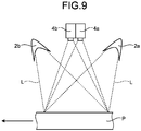
- this surface defect detection device 1 serving as the first embodiment of the present invention is a device that detects a surface defect of a cylindrical steel pipe P conveyed in the direction of the arrow in FIG. 1 , and includes, as main components, light sources 2a and 2b, a function generator 3, area sensors 4a and 4b, an image processing device 5, and a monitor 6.
- the light sources 2a and 2b emit distinguishable illumination light beams L to the same inspection target portion on a surface of the steel pipe P according to trigger signals from the function generator 3.
- the light sources 2a and 2b are preferably symmetrically arranged with respect to the inspection target portion. Accordingly, the light sources 2a and 2b are arranged so as to be displaced by the same angle from a vector normal to the surface of the steel pipe P, and such that irradiation direction vectors of the illumination light beams L and the vector normal to the surface of the steel pipe P lie in the same plane.
- the purpose of the sameness of angles of incidence as mentioned herein is to make optical conditions as equal as possible when the light sources oriented in the different directions sources are distinguished from each other, and to greatly reduce a signal of a sound portion including scale and a harmless pattern by performing difference processing.
- the signal of the sound portion greatly depends on surface characteristics of the target, and thus, the sameness is difficult to be unconditionally guaranteed by a constant angle. Therefore, if a condition allows inspection, the angles are expressed as the same angle as long as the signal of the sound portion can be reduced by the difference processing even if the angles differ from each other to a certain degree.
- the condition allowing inspection as mentioned herein refers to a condition that a specular reflection component can be sufficiently eliminated, and the angles of incidence may be increased as much as possible if the light quantity is sufficient.
- the number of the light sources is two, but the number of the light sources may be three or larger if the light sources are distinguishable from one another.
- the distinguishable light sources as mentioned herein refer to light sources, for each of which the reflected light quantity of a reflected light beam obtained from the target can be separately found.
- the area sensors 4a and 4b photograph two-dimensional images formed by the reflected light beams of the illumination light beams L emitted from the light sources 2a and 2b according to the trigger signals from the function generator 3.
- the area sensors 4a and 4b enter data of the photographed two-dimensional images into the image processing device 5.
- the area sensors 4a and 4b are preferably arranged, if possible, on the normal vector of the inspection target portion in a state where imaging fields of view of the respective area sensors 4a and 4b are ensured.
- the area sensors 4a and 4b are located as close as possible to each other, and optical axes thereof are preferably oriented as parallel as possible to each other. As illustrated in FIG. 2 , the optical axes of the area sensors 4a and 4b may be adjusted to be coaxial using any of a semitransparent mirror 10, a beam splitter, and a prism. Due to this, a difference image to be described later can be accurately acquired.
- the image processing device 5 is a device that detects a surface defect in the inspection target portion by performing the difference processing (to be described later) between the two two-dimensional images received from the area sensors 4a and 4b.
- the image processing device 5 outputs the two-dimensional images received from the area sensors 4a and 4b and information on a detection result of the surface defect to the monitor 6.
- the surface defect detection device 1 having the configuration described above distinguishes the scale or the harmless pattern from the surface defect in the inspection target portion by performing surface defect detection processing to be described below.
- the surface defect as mentioned herein refers to a concavo-convex defect.
- the scale or the harmless pattern refers to a portion having a surface film or surface characteristics with optical characteristics different from those of a base steel portion with a thickness of roughly several micrometers to several tens of micrometers, and is a portion causing noise in the surface defect detection processing.
- the following describes surface defect detection processing serving as first to third modes of the present invention.
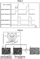
- FIG. 3 is a timing diagram illustrating drive timing of the light sources 2a and 2b and the area sensors 4a and 4b.
- d denotes a light-emitting time of the light sources 2a and 2b
- T denotes a photographing period of the two-dimensional images photographed by the area sensors 4a and 4b.
- the light sources 2a and 2b are distinguished from each other by using the light sources 2a and 2b as flash light sources, and by repeatedly emitting light from the flash light sources such that the light emitting times of the flash light sources do not overlap each other.
- the function generator 3 transmits a trigger signal to the light source 2a and the area sensor 4a, the light source 2a emits one of the illumination light beams L, and the area sensor 4a completes the photographing of a two-dimensional image within the time d.
- the function generator 3 transmits a trigger signal to the light source 2b and the area sensor 4b, and a two-dimensional image is photographed in the same manner.
- the two-dimensional images formed by the individual reflected light beams corresponding to the illumination light beams L emitted from the respective light sources can be photographed with the time difference d without a reduction in light quantity.
- the light-emitting time d of the flash light sources is preferably short. This is because reducing the light-emitting time d reduces a shutter delay between the two two-dimensional images obtained by the area sensors 4a and 4b, and reduces a positional displacement between the two-dimensional images caused by the shutter delay.
- the light-emitting time d of the flash light sources needs to satisfy a condition represented by Expression (2) below.
- the size of a surface defect to be detected is, for example, 20 mm
- signals of at least 5 ⁇ 5 pixels are empirically required for detecting the surface defect. Therefore, only a resolution of 4 mm/pixel is needed.
- the allowable amount of the positional displacement caused by the light emission timing of the illumination light beams L empirically needs to be within 0.2 pixels. Therefore, if the conveyance speed of the steel pipe P is 1 m/s, 3 m/s, or 5 m/s, the light-emitting time of the light sources 2a and 2b needs to be equal to or shorter than 800 ⁇ s, 270 ⁇ s, or 160 ⁇ s, respectively. If the conveyance speed and the conveyance direction of the steel pipe P are constant, this positional displacement can be corrected after the two-dimensional images are photographed.
- the image processing device 5 detects the surface defect in the inspection target portion by performing the difference processing between the two-dimensional images.
- Ia(x,y) denote a luminance value of each pixel constituting a two-dimensional image Ia obtained when the illumination light beams L is emitted from the light source 2a (where the number of pixels is X ⁇ Y, the x-coordinate satisfies 1 ⁇ x ⁇ X, and the y-coordinate satisfies 1 ⁇ y ⁇ Y), and Ib(x,y) denote a luminance value of each pixel constituting a two-dimensional image Ib obtained when the illumination light beam L is emitted from the light source 2b, a luminance value I_diff(x,y) of each pixel of a difference image I_diff therebetween is represented by Expression (3) given below.
- I _ diff x , y Ia x , y ⁇ Ib x , y
- FIG. 4 illustrates examples of the two-dimensional images Ia and Ib obtained by photographing the surface defect, and the scale and the harmless pattern that are not defects, and the difference image I_diff therebetween, in (a), (b), and (c), respectively.
- the surface defect portion however, the surface has a concavo-convex shape.
- the scale and the harmless pattern that are not defects are removed, and the surface defect alone can be detected.
- the surface defect alone is detected in this manner; a final evaluation is made on the basis of various feature quantities as to whether the surface defect is harmful; and the evaluation result is displayed on the monitor 6.
- a two-dimensional low pass filter is preferably used to reduce the influence of the positional displacement between the two-dimensional images.
- H denote the two-dimensional low-pass filter
- I'_diff(x,y) of the difference image is represented by Expression (4) given below.
- the light sources 2a and 2b preferably use the same light source, and each of the light sources preferably emits light so as to obtain light beams as uniform and parallel as possible.
- the inspection target portion is preferably approximately planar. However, even in an application to a case where the surface is somewhat nonuniform or to a smooth curved surface such as that of the steel pipe P, the surface defect can be detected through general shading correction.
- the angle of incidence of the illumination light beams L is preferably in a range preventing a specular reflection component from being included in reflected light from the sound portion and enabling ensuring of a sufficient light quantity.
- the inventors of the present invention conducted an experiment to investigate a relation between the angle of incidence of the illumination light beams L and reflectance of the sound portion (base steel portion).
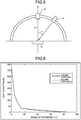
- FIG. 5 illustrates the configuration of a device used in the experiment. As illustrated in FIG. 5 , in this experiment, a power meter 12 was fixed in a position on a normal vector 1 of a target position on a surface of a slab sample 14. The light quantity received by the power meter 12 was measured while an angle of incidence ⁇ of a laser 13 relative to the normal vector l was varied from 0° to 90°.
- FIG. 5 illustrates the configuration of a device used in the experiment. As illustrated in FIG. 5 , in this experiment, a power meter 12 was fixed in a position on a normal vector 1 of a target position on a surface of a
- FIG. 6 illustrates results of the experiment.
- the angle of incidence ⁇ is in a range of 0° to 20°
- the light quantity received by the power meter 12 is large due to inclusion of the specular reflection component, but, when the angle of incidence ⁇ is 60° or larger, the light quantity received by the power meter 12 greatly drops. Therefore, the light quantity received can be increased by reducing the angle of incidence of the illumination light beams L unless any problem occurs in detectivity.
- the resolution in the depth direction of the inspection target portion depends on the inclination angle of the defect and resolutions of the area sensors 4a and 4b.
- the inclination angle of the defect refers to an angle obtained by orthographically projecting "a normal vector of the defect portion" to "a plane formed by a normal vector of a sound portion surface of the inspection target portion and a light source direction vector", and by taking an angle formed between the orthographically projected vector and the normal vector of the sound portion surface.
- the following describes the surface defect detection processing serving as the second mode of the present invention with reference to FIG. 7 .
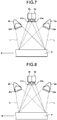
- the light sources 2a and 2b are distinguished from each other by using light sources having wavelength ranges not overlapping each other as the light sources 2a and 2b.
- two types of wavelength selection filters 20a and 20b having wavelength ranges not overlapping each other are placed on the light sources 2a and 2b to select wavelength ranges of the illumination light beams L.
- Wavelength selection filters 21a and 21b having the same wavelength selection characteristics are placed on the area sensors 4a and 4b.
- Such a configuration causes the reflected light beam of the illumination light beam L from the light source 2a to be received by only the area sensor 4a through the wavelength selection filters 20a and 21a, and causes the reflected light beam of the illumination light beam L from the light source 2b to be received by only the area sensor 4b through the wavelength selection filters 20b and 21b. Consequently, by matching the photographing timing of the area sensors 4a and 4b with each other, the two-dimensional images formed by the reflected light beams of the illumination light beams L from the light sources 2a and 2b can be photographed without any positional displacement. Processing after the two-dimensional images are photographed is the same as that of the first mode.
- the light sources 2a and 2b may be used as the flash light sources, and photographing times of the two-dimensional images may be reduced without changing the light emission timing of the light sources 2a and 2b.
- a configuration may be employed in which a blue color transmitting filter is used as the wavelength selection filter 20a, a green color transmitting filter is used as the wavelength selection filter 20b, and the two-dimensional images are photographed using one color camera so that only the reflected light beam of the illumination light beam L from the light source 2a is received in the blue channel, and only the reflected light beam of the illumination light beam L from the light source 2b is received in the green channel.
- the following describes the surface defect detection processing serving as the third mode of the present invention with reference to FIG. 8 .
- the light sources 2a and 2b are distinguished from each other by using mutually orthogonal linear polarization characteristics as the light sources 2a and 2b.
- linear polarizing plates 30a and 30b are placed at ⁇ ° and ( ⁇ + 90)° (where ⁇ is any angle) on the light sources 2a and 2b, respectively, and only light of mutually orthogonal polarization components is transmitted therethrough.
- a linear polarizing plate refers to a filter that transmits only a linear polarization component in a certain direction with respect to incident light.
- Linear polarizing plates 31a and 31b having the same linear polarization characteristics as those of the linear polarizing plates 30a and 30b are placed at ⁇ ° and ( ⁇ + 90)° on the area sensors 4a and 4b.
- Such a configuration causes the reflected light beam of the illumination light beam L from the light source 2a to be received by only the area sensor 4a, and causes the reflected light beam of the illumination light beam L from the light source 2b to be received by only the area sensor 4b. Consequently, by matching the photographing timing of the area sensors 4a and 4b with each other, the two-dimensional images formed by the reflected light beams of the illumination light beams from the respective light sources can be photographed without any positional displacement.
- the light sources 2a and 2b may be used as the flash light sources, and the photographing times of the two-dimensional images may be reduced without changing the light emission timing of the light sources 2a and 2b.
- positioning and processing after the two-dimensional images are photographed are the same as those of the first and second modes.
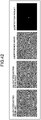
- FIG. 10 illustrates results of the surface defect detection processing. Part (a) in FIG. 10 illustrates a two-dimensional image obtained when the illumination light beam L is emitted from the light source 2a; part (b) in FIG. 10 illustrates a two-dimensional image obtained when the illumination light beam L is emitted from the light source 2b; and part (c) in FIG.
- S/N ratios of the images illustrated in parts (a) to (c) of FIG. 10 were 3.5, 3.5, and 6.0, in that order.
- S/N ratio of the difference image was improved from those in the cases in each of which the illumination light beam L was simply emitted from one direction.
- FIG. 11 is a diagram illustrating results of the surface defect detection processing for a steel pipe portion where scale has been generated.
- Part (a) in FIG. 11 illustrates a two-dimensional image obtained when the illumination light beam L is emitted from the light source 2a;
- part (b) in FIG. 11 illustrates a two-dimensional image obtained when the illumination light beam L is emitted from the light source 2b;
- part (c) in FIG. 11 illustrates a difference image between the two-dimensional image illustrated in part (a) of FIG. 11 and the two-dimensional image illustrated in part (b) of FIG. 11 .
- Black spots spreading over the whole two-dimensional images illustrated in parts (a) and (b) in FIG. 11 are the scale serving as noise. Since the scale had a flat shape, the image of the scale was removed by acquiring the difference image. In the difference image, the signal of the scale serving as the noise was reduced to a quarter of a case where the illumination light beam L was simply emitted from one direction.
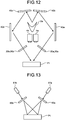
- FIG. 12 is a schematic diagram illustrating the configuration of a modification of the surface defect detection device serving as the first embodiment of the present invention.
- illumination light emitted from the single light source 2a is divided by a plurality of mirrors 40a, 40b, 40c, and 40d, and an inspection target portion of a steel pipe P1 is finally irradiated with the illumination light from two directions.
- the same effect as that of the second and third modes can be obtained by arranging the wavelength selection filters 20a and 20b and the linear polarizing plates 30a and 30b on respective optical paths of the illumination light.
- the illumination light is emitted from two directions in the present modification, the same applies to a case where illumination light is emitted from three or more directions.
- FIG. 13 is a schematic diagram illustrating the configuration of another modification of the surface defect detection device serving as the first embodiment of the present invention.
- the wavelengths of light sources are limited using pulse lasers 51a and 51b and diffusion plates 50a and 50b.
- the light sources are distinguished from each other by irradiating the inspection target portion from the right and left directions thereof with laser beams from the two pulse lasers 51a and 51b having wavelength ranges different from each other.
- the diffusion plates 50a and 50b are inserted in optical paths of the laser beams.
- the illumination light is emitted from two directions in the present modification, the same applies to a case where illumination light is emitted from three or more directions.
- a dichroic mirror is used instead of the wavelength selection filters 21a and 21b placed on the area sensors 4a and 4b in the surface defect detection device illustrated in FIG. 7 .
- the dichroic mirror refers to a mirror that reflects light having a particular wavelength component and transmits light having the other wavelength components. Using the dichroic mirror eliminates the necessity of the wavelength selection filters.
- the illumination light is emitted from two directions in the present modification, the same applies to a case where illumination light is emitted from three or more directions.
- the following describes the configuration and operations of a surface defect detection device serving as the second embodiment of the present invention with reference to FIGS. 14 to 22 .
- the configuration of the surface defect detection device of the present embodiment is the same as the configuration of the surface defect detection device of the above described first embodiment. Thus, the following omits the description of the configuration, and describes only the operations of the surface defect detection device.
- the surface defect detection device 1 serving as the second embodiment of the present invention distinguishes scale or a harmless pattern from a concavo-convex surface defect in the inspection target portion by performing surface defect detection processing to be described below.
- the scale or the harmless pattern refers to a portion having a surface film or surface characteristics with optical characteristics different from those of a base steel portion with a thickness of roughly several micrometers to several tens of micrometers, and is a portion causing noise in the surface defect detection processing.
- the image processing device 5 After applying image processing, such as calibration, shading correction, and denoising, to the two two-dimensional images received from the area sensors 4a and 4b using the camera parameters derived in advance, the image processing device 5 generates the difference image by performing difference processing between the two-dimensional images, and detects the concavo-convex surface defect in the inspection target portion from the generated difference image.
- image processing such as calibration, shading correction, and denoising
- Ia(x,y) denote a luminance value of each pixel constituting the two-dimensional image Ia obtained when the illumination light beams L is emitted from the light source 2a (where the number of pixels is X ⁇ Y, the x-coordinate satisfies 1 ⁇ x ⁇ X, and the ⁇ -coordinate satisfies 1 ⁇ y ⁇ Y), and Ib(x,y) denote a luminance value of each pixel constituting the two-dimensional image Ib obtained when the illumination light beam L is emitted from the light source 2b, then the luminance value I_diff(x,y) of each pixel of the difference image I_diff obtained by the difference processing is represented by Expression (3), which is already given.
- the surface defect portion however, the surface has a concavo-convex shape.
- Parts (a) and (b) in FIG. 14 depict diagrams illustrating shades and shadows when the illumination light is emitted from either of the light sources to the inspection target portion in cases where the surface shape of an inspection target portion is concave and convex, respectively.
- the near side of the light source is darker due to reduction in light quantity of the illumination light, and the far side of light source is brighter because of being closer to a specular reflection direction.
- the near side of the light source is brighter because of being closer to a specular reflection direction
- the far side of light source is darker because of being shaded by the convex shape.
- the brightness pattern of the reflected light beam of the illumination light beam differs between the case where the surface shape of the inspection target portion is concave and the case where the surface shape thereof is convex. Therefore, presence or absence of a concavo-convex surface defect can be detected by recognizing the brightness pattern of the reflected light beam.
- the following describes a method for detecting a concavo-convex surface defect by recognizing the brightness pattern of the reflected light beam.
- a concavo-convex surface defect is detected.
- a convex surface defect can be detected using the same logic.
- a bright portion to be mentioned below refers to a blob that is obtained by performing connection processing of pixels having luminance of a predetermined threshold or higher in the difference image I_diff and that has an area equal to or larger than a predetermined value.
- a dark portion to be mentioned below refers to a blob that is obtained by performing the connection processing of pixels having luminance of a predetermined threshold or lower in the difference image I_diff and that has an area equal to or larger than a predetermined value.
- the blob refers to a collection of labeled pixels.
- the brightness pattern is recognized by extracting the bright portion and the dark portion by performing threshold processing.
- the light sources 2a and 2b are right-left symmetrically arranged with respect to the normal vector of the inspection target portion, and consequently, the brightness pattern of the reflected light resulting from the concavo-convex shape of the surface is generated in the right-left direction.
- the right and the left of the bright/dark contrast are reversed according to the order of the difference processing.
- the surface shape is assumed to be concave if the right side is bright and the left side is dark, and is assumed to be convex if the right side is dark and the left side is bright.
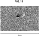
- the difference image I_diff of a concave surface defect is as illustrated in FIG. 15 .
- the and -The, binarized images I_blight and I_dark of the bright and the dark portions, respectively, are represented by Expression (5) given below.
- I _ blight x , y 0 when I _ diff x , y ⁇
- the I _ blight x , y 1 when I _ diff x , y ⁇
- the I _ dark x , y 1 when I _ diff x , y ⁇ ⁇
- the I _ dark x , y 0 when I _ diff x , y > ⁇
- the images of the bright and the dark portions are binarized in this manner, and are subjected to connection and isolated point removal as needed. Then, the positional relation between the bright and the dark portions is calculated to detect the presence or absence of a concavo-convex surface defect.
- Various methods are available as a method for calculating the positional relation between the bright and the dark portions. The following describes three representative calculation methods, but other calculation methods may be used as long as the other methods are capable of calculating the positional relation between the bright and the dark portions.
- a first positional relation calculation method is a method for calculating the positional relation between the bright and the dark portions by applying expansion processing in a certain direction to the bright and the dark portions.
- FIG. 16 illustrates the flowchart of this calculation method. Since a concave surface defect is detected in the present embodiment, a case will be described where a brightness pattern with the right side being bright and the left side being dark is recognized. The expression "the right side being bright and the left side being dark” means that the dark portion is always present on the left side of the bright portion, and the bright portion is always present on the right side of the dark portion.
- the image processing device 5 applies the expansion processing in the rightward direction to the dark portion, and applies the expansion processing in the leftward direction to the bright portion (Steps S1a and S1b).
- I_blight_extend and I_dark_extend denote images of the bright and the dark portions, respectively, and W denote an expansion length
- the expansion processing is expressed by Expression (6) given below.
- Expression (6) assuming the upper left corner of the two-dimensional image to be the origin, the downward direction is assumed to be positive in the y-axis direction, and the rightward direction is assumed to be positive in the x-axis direction.
- the bright and the dark portions are expanded by the same length W.
- the expansion length W need not be the same for both the bright and the dark portions.
- the expansion processing may be applied to only one of the bright and the dark portions.
- the expansion length W also depends on the size of the surface defect desired to be detected.
- the image processing device 5 performs AND processing on the images I_blight_extend and I_dark_extend of the bright and the dark portions that have been subjected to the expansion processing as represented by Expression (7) given below, and thereby extracts, as a defect candidate portion image I_defect, an overlapping portion between the images I_blight_extend and I_dark_extend of the bright and the dark portions that have been subjected to the expansion processing (Steps S2a and S2b) .
- I _ defect I _ blight _ e x t e n d & I _ dark _ extend
- the image processing device 5 performs labeling processing to generate a defect candidate blob I_defect_blob (Step S3).
- the image processing device 5 extracts feature quantities of each of the defect candidate blobs I_defect_blob, and determines, on the basis of the extracted results, whether each of the defect candidate blobs I_defect_blob is a concave surface defect (Steps S4a and S4b). Since information on the bright and the dark portions is needed to investigate the feature quantities of the defect candidate blob I_defect_blob, the bright and the dark portions are restored from the defect candidate blob I_defect_blob.
- the image processing device 5 searches the defect candidate blob I_defect_blob starting from the centroid thereof toward the left side thereof for the dark portion binarized image I_dark, and regards the first found blob as a dark portion defect candidate blob I_dark_blob.
- the image processing device 5 searches the defect candidate blob I_defect_blob starting from the centroid thereof toward the right side thereof for the bright portion binarized image I_blight, and regards the first found blob as a bright portion defect candidate blob I_blight_blob.
- the image processing device 5 extracts feature quantities from the bright portion defect candidate blob I_blight_blob and the dark portion defect candidate blob I_dark_blob that have been restored as described above, and determines, on the basis of the extracted feature quantities, whether each of the defect candidate blobs I_defect_blob is a concave surface defect. Specific feature quantities differ depending on the defect, and thus will not be described here, but one example will be given in an example to be described later.
- a second positional relation calculation method after the above-described threshold processing is performed and the connection and isolated point removal processing is performed as needed, the bright and the dark portions are extracted and subjected to labeling, and the positional relation between the bright and the dark portions is recognized so as to detect the concave surface defect.
- the image processing device 5 individually recognizes the bright and the dark portions by the labeling, and obtains centroid information on the bright and the dark portions.
- the image processing device 5 determines, on the basis of the centroid information on the bright and the dark portions, whether the centroid of the dark portion is present in a predetermined range on the right side of each bright portion.
- the image processing device 5 recognizes a combination of the bright and the dark portions forming a pair as a brightness pattern, and performs a feature quantity analysis of the brightness pattern to determine whether the brightness pattern is a concave surface defect.
- the brightness pattern is recognized using the centroid information here, the information used for the recognition of the brightness pattern need not be the centroid information as long as the positions of the bright and the dark portions can be obtained using the information (such as upper end positions or lower end positions thereof).
- the concave surface defect is detected by recognizing the brightness pattern using a filter without performing the above-described threshold processing.
- the surface defect detection device 1 illustrated in FIG. 1 since the light sources 2a and 2b are right-left symmetrically arranged with respect to the normal line of the inspection target portion, the brightness pattern resulting from concavity and convexity of the surface is generated in the right-left direction.
- FIGS. 17(a) and 17(b) are diagrams respectively illustrating an example of a difference image and a one-dimensional profile of a brightness pattern on a line segment L4 illustrated in FIG. 17(a) .
- the one-dimensional profile of the brightness pattern is a characteristic one-dimensional profile in which the right side is chevron-shaped and the left side is valley-shaped.
- a filter H with the right side being chevron-shaped and the left side being valley-shaped is generated in advance, and the filter H is applied to the difference image I_diff as represented by Expression (8) below so as to generate a two-dimensional image I_cont in which high-frequency noise is reduced and only the brightness pattern is emphasized.
- I _ cont H * I _ diff
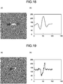
- FIGS. 18(a) and 18(b) are diagrams respectively illustrating an example of a two-dimensional image of the filter H generated in advance and a one-dimensional profile in the right-left direction thereof.
- FIGS. 19(a) and 19(b) are diagrams respectively illustrating an example of a difference image having been subjected to filtering using the filter H illustrated in FIGS. 18(a) and 18(b) , and a one-dimensional profile in the right-left direction thereof. As illustrated in FIGS. 19(a) and 19(b) , it is found that a two-dimensional image is obtained in which high-frequency noise is reduced and only the brightness pattern is emphasized.
- the image processing device 5 applies, as needed, the connection and isolated point removal processing to the two-dimensional image in which the brightness pattern is emphasized as described above, and then, extracts the defect candidate portion image I_defect by performing the threshold processing.
- the image processing device 5 detects the concave surface defect by applying the same processing as that of the first positional relation calculation method to the extracted defect candidate portion image I_defect.
- the two distinguishable light sources 2a and 2b are used to emit the illumination light beams L at substantially the same angle of incidence from different directions to the same inspection target portion; the images formed by the reflected light beams of the respective illumination light beams L are acquired; the bright portion and dark portion of the image obtained by performing the difference processing between the acquired images are extracted; and the presence or absence of the concavo-convex surface defect is determined on the basis of the positional relation between the bright portion and the dark portion thus extracted and the irradiation directions of the illumination light beams L.
- the scale or the harmless pattern can be accurately distinguished from the concavo-convex surface defect.
- the right-left brightness pattern is recognized because the light sources are right-left symmetrically arranged.
- the concavo-convex surface defect can be detected by the same processing. Specifically, if the light sources are upper-lower symmetrically arranged, the brightness pattern only changes from the right-left direction to the upper-lower direction. Therefore, the same processing can be used to detect the concavo-convex surface defect by rotating the brightness pattern by 90°.
- the near side is darker and the far side is brighter if the surface defect is concave, and the near side is brighter and the far side is darker if the surface defect is convex.
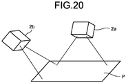
- the two-dimensional image obtained by the illumination light beam from the light source 2a is as illustrated in (a) of FIG. 21
- the two-dimensional image obtained by the illumination light beam from the light source 2b is as illustrated in (b) of FIG. 21 .
- the difference image has a brightness pattern with a contrast in a direction from the lower left to the upper right, as illustrated in (c) of FIG. 21 .
- the concave surface defect can be detected using the same method as that for the brightness pattern in the right-left direction.
- difference images having a plurality of respective patterns can be obtained by using three or more light sources. Thus, accuracy of detection of a surface defect can be further improved.
- the concavo-convex surface defect is detected in the case where the illumination light beams are emitted from the directions symmetrical with respect to the normal line of the inspection target portion.
- the irradiation directions of the illumination light beams need not be symmetrical.
- the surface defect detection processing of the present embodiment is generally applicable to manufacturing lines for steel products regardless of whether they are hot or cold.
- the surface defect detection processing using the above-described first positional relation calculation method was applied to an inspection target portion where a pit flaw is formed and to a sound inspection target portion where no pit flaw is formed.
- a luminance ratio, an area ratio, and degrees of roundness of the bright and the dark portions were calculated as the feature quantities.
- the degrees of roundness are values obtained by dividing areas of the bright and the dark portions by squares of lengths of circumferences thereof and by normalizing the results, and are used in determining whether shapes of the bright and the dark portions are close to circular shapes. If surface defects are due to the same cause, luminance and areas thereof are unlikely to be significantly different between the right and left signals.
- FIG. 22 illustrates the detection results. As illustrated in FIG. 22 , according to this example, a pit flaw and a sound portion where no pit flaw is formed have been found to be accurately distinguishable from each other.
- FIG. 23 is a diagram illustrating a result of detecting a surface defect called a dent flaw using the surface defect detection method according to the present invention.
- the dent flaw is found to be surely detectable using a brightness pattern.
- a defect signal of a surface defect called a roll mark can hardly be found because the shape of the roll mark is slender, as illustrated in FIG. 24(a) , but, when the illumination light is emitted in the longitudinal direction of the thick steel plate, the strength of the defect signal increases as illustrated in FIG. 24(b) .
- the inventors of the present invention measured the shape of the surface defect, and calculated the inclination of the surface defect when the illumination light was emitted from the width direction of the thick steel plate and when the illumination light was emitted from the longitudinal direction of the thick steel plate.
- the inclination as mentioned herein refers to an angle formed between two vectors obtained by orthogonally projecting the normal vector of each surface of the thick steel plate and the normal vector of a reference surface of the thick steel plate to a plane formed by the light source, the area sensor, and the inspection target position.
- FIGS. 25(a) and 25(b) illustrate the calculated results. As illustrated in FIG.
- the inclination of the surface defect was 7° or smaller when the illumination light was emitted from the width direction of the thick steel plate, whereas, as illustrated in FIG. 25(b) , the inclination of the surface defect was 20° to 30° when the illumination light was emitted from the longitudinal direction of the thick steel plate.
- a pattern looking like stripes when the illumination light was emitted from the width direction of the thick steel plate is harmless scale peeling.
- the shape of the sound portion was measured in the same manner, and the inclination of the sound portion when the illumination light was emitted from the width direction of the thick steel plate was evaluated. As a result, as illustrated in FIG.
- the inclination of the sound portion was 3° to 5°, which was comparable with the inclination of the surface defect when the illumination light was emitted from the width direction of the thick steel plate. Therefore, the difference in inclination of the surface defect is considered to affect the detectivity of the surface defect.
- the following describes a physical phenomenon related to the detectivity of the surface defect.
- a model of an optical system is established to study the physical phenomenon more in detail.
- the study herein uses a simplified model of the Torrance-Sparrow model serving as one of reflection models in accordance with the physical phenomenon that are widely used in optical simulations (refer to reference literature ( Sato et al., "Illumination Distribution from Shadows", IPSJ Journal: Computer Vision and Image Media, Vol. 41, No. SIG 10, Dec. 2000 )).
- the optical system should be normally treated as a three-dimensional model, a two-dimensional model will be used below for the sake of simplicity.
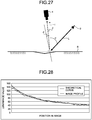
- FIG. 27 is a diagram illustrating the configuration of the two-dimensional model of the optical system.
- ⁇ denote an angle of incidence of the illumination light beam L from a light source 2 with respect to a steel product surface S (normal vector 1)
- ⁇ denote an angle of reflection of the illumination light beam L incident into an area sensor 4
- ⁇ denote an inclination of the inspection target portion as microscopically measured assuming the inclination of the reference surface of the steel product surface S to be
- I 0 denote an incident light quantity of the illumination light beam L from the light source 2 into the inspection target portion
- k (K 1 ,K 2 , ⁇ ) denote a parameter (vector quantity) representing the surface characteristics of the inspection target portion
- a light quantity i of the illumination light beam L incident into the area sensor 4 is represented by Expression (9) given below.
- i I 0 R ⁇ , ⁇ , ⁇ , k
- R in Expression (9) represents a function for reflection intensity of the illumination light beam L, and is calculated by Expression (10) given below.
- R ⁇ , ⁇ , ⁇ , k K 1 cos ⁇ ⁇ ⁇ + K 2 1 cos ⁇ ⁇ ⁇ e ⁇ ⁇ ⁇ ⁇ + ⁇ 2 2 2 ⁇ 2
- the first term in the right-hand member of Expression (10) represents an intensity of diffuse reflection of the illumination light beam L
- the second term thereof represents an intensity of specular reflection of the illumination light beam L
- the reflection intensity of the illumination light beam L is represented as the sum of the first and second terms.
- the illumination light beam L diffuses in all directions after entering the inspection target portion.
- the specular reflection the illumination light beam L is reflected most strongly in the symmetrical direction with respect to the normal vector of the inspection target portion, and the intensity of the illumination light beam L is attenuated in a Gaussian manner as the direction of the light beam departs from the symmetrical direction.
- the term k (K 1 ,K 2 , ⁇ ) is a term resulting from the surface characteristics of the inspection target portion, and determines the degree of spreading of the specular reflection and the intensity ratio between the specular reflection and the diffuse reflection. However, if the angle of incidence ⁇ and the inclination ⁇ satisfy a condition ⁇ /2 ⁇ ⁇ + ⁇ or ⁇ + ⁇ ⁇ - ⁇ /2, the reflection intensity of the illumination light beam L is 0 because the inspection target portion is shaded.
- I 1 and I 2 denote incident light quantities of the illumination light beams L into the target surface; ⁇ 1 and ⁇ 2 denote angles of incidence of the illumination light beams into the target position on the target surface; ⁇ denotes the angle of reflection of the illumination light beam L incident into the area sensor 4; ⁇ denotes the inclination of the target surface as microscopically measured assuming the inclination of the reference surface of the target surface to be 0; and k denotes the parameter representing the surface characteristics of the target surface.
- the shading correction is subsequently applied to the illuminance i 1 and i 2 to eliminate light quantity unevenness of the light source 2 and unevenness in optical conditions. While various methods are available for the shading correction, the shading correction was applied here using a commonly used method in which a row vector (called a "vertical direction average vector") is created by summing the luminance of respective pixels in the vertical direction and calculating the average luminance, and all rows of the image are subjected to subtraction and division using the vertical direction average vector, and further, signals are multiplied by a constant to be normalized. The same processing was applied to the resultant image for the horizontal direction thereof, and thus, the shading correction was performed.
- a row vector called a "vertical direction average vector”
- i 10 and i 20 denote signals in the case where the target surface was a sound portion, and ko denote the surface characteristics of the sound portion, then the signals i 10 and i 20 are represented as Expressions (13) and (14) given below.
- i 10 I 1 R ⁇ 1 , ⁇ ,0, k 0
- i 20 I 2 R ⁇ 2 , ⁇ ,0, k 0
- Expressions (15) to (17) luminance values on images after being subjected to the shading correction and the difference image therebetween are represented as Expressions (15) to (17) given below.
- Expression (15) represents the luminance i 1 after the shading correction.
- Expression (16) represents the luminance i 2 after the shading correction.
- Expression (17) represents the luminance on the difference image.
- the above-described model was used to derive an optimal range of the angle of incidence of the illumination light beam from strengths of image signals of the sound portion and the surface defect portion.
- the parameter representing the surface characteristics of the steel product surface was experimentally obtained. Specifically, an image of a steel product having general surface characteristics was actually photographed, and a luminance profile (image profile) of an actual image signal was fitted with a luminance profile (theoretical curve) of a theoretical image signal obtained by simulating the same optical system.
- FIG. 28 illustrates the result of the fitting
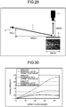
- FIG. 29 illustrates the configuration of the optical system used in the experiment.
- the obtained parameter k representing the surface characteristics was used to simulate changes in signal strength with a change in slope angle (inclination) of the surface defect when the angle of incidence ⁇ of the illumination light was 45°, 60°, and 75°.
- a contributing term in this surface defect detection processing is the inclination of the steel product surface.
- FIG. 30 is a diagram illustrating the changes in signal strength with the change in slope angle of the surface defect when the angle of incidence ⁇ of the illumination light into the defect position is 45°, 60°, and 75°.
- the signal strength increases as the slope angle of the surface defect increases. That is, if the illumination light is emitted from the width direction of the thick steel plate, that is, from the width direction with respect to the roll mark, the signal strength does not greatly differ from that of the surface characteristics because the inclination of the surface defect portion is equal to the inclination of the surface characteristics. In contrast, if the illumination light is emitted from the longitudinal direction of the thick steel plate, the signal strength is larger because the inclination of the surface defect portion is larger than the inclination of the sound portion, and thus, the surface defect can be detected.
- this example is an example of a surface defect that is long in the width direction of the thick steel plate
- a surface defect that is long in the longitudinal direction of the thick steel plate is present in the same manner. Therefore, to prevent surface defects from being missed and to detect all surface defects, the illumination light needs to emitted from two directions of the width and longitudinal directions of the thick steel plate. Since a surface defect that is long in an oblique direction is also present, the overlooking also occurs if the illumination light is simply emitted from an oblique direction. Therefore, also in this case, the illumination light needs to be emitted from two directions of the width and longitudinal directions of the thick steel plate.
- the present invention is characterized in acquiring the difference image by emitting the illumination light from two different directions to the inspection target portion.
- conditions of the optical system will be studied by way of an example for the sake of simplicity in which the illumination light is emitted from mutually symmetrical oblique directions with respect to the normal vector of the steel product surface.
- conditions for incidence and reflection of the illumination light are preferably the same between when the illumination light is emitted from one of the light sources (for convenience, emitted from the right direction) and when the illumination light is emitted from the other of the light sources (for convenience, emitted from the left direction).
- FIGS. 31(a) and 31(b) illustrate examples in which the present invention is applied to the thick steel plate.
- FIG. 31(a) illustrates a reflection model of the illumination light on the sound portion surface.
- FIG. 31(b) illustrates a reflection model of the illumination light on a highly diffusive surface.
- the thickness of lines represents the light quantity of the illumination light.
- the condition of an illumination light beam L2 from the right direction is close to a specular reflection condition, and consequently, the intensity of a reflected light beam RL2 on the highly diffusive surface is lower than the intensity of the reflected light beam RL2 in the sound portion.
- the condition of an illumination light beam L1 from the left direction is close to a diffusive reflection condition, and consequently, the intensity of a reflected light beam RL1 on the highly diffusive surface is higher than the intensity of the reflected light beam RL1 in the sound portion.
- the specular reflection condition mentioned above refers to a condition where the light source and the area sensor reside in symmetrical positions with respect to the normal vector of the sound portion surface, that is, a condition where the angle of incidence and the angle of reflection of the illumination light are equal to each other.
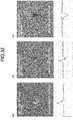
- FIGS. 32(a) to 32(c) illustrate examples of difference images obtained from the thick steel plate. In the examples illustrated in FIGS.
- the appearance of the surface defect varies with the position in the field of view.
- the left side of the field of view ( FIG. 32(a) ) is bright as a whole, and the right side thereof ( FIG. 32(c) ) is dark as a whole.
- the reason is that the diffusivity of the surface defect portion is high, and therefore, the signal strength is larger than that of the sound portion when the condition is farther from the specular reflection condition. Due to this, although the brightness pattern can be surely seen at the center of the field of view ( FIG. 32(b) ), an offset in luminance of the image is generated by the diffusivity, so that each end of the field of view includes only the bright portion or the dark portion. Accordingly, the surface defect is difficult to be detected at each end of the field of view because the surface defect is detected using the brightness pattern in the present invention.
- FIGS. 33(a) and 33(b) are diagrams respectively illustrating images obtained when the illumination light is emitted from the right side direction and the left side direction to the thick steel plate with a surface without concavity and convexity to which highly diffusive scale is attached.
- FIGS. 34(a) to 34(c) are diagrams illustrating an image obtained when the illumination light is emitted from the right side direction, an image obtained when the illumination light is emitted from the left side direction, and a difference image therebetween.
- the left side in the screen is expressed as the "near side”
- the right side in the screen is expressed as the "far side”
- the left side in the screen is expressed as the "far side”
- the right side in the screen is expressed as the "near side”.
- FIG. 35 illustrates the optical system used in the experiment. As illustrated in FIG. 35 , the area sensor 4 was placed such that the normal vector 1 to a center Sc of a test sample S coincides with the optical axis of the area sensor 4. In addition, two light sources 2 were placed in symmetrical positions with respect to the optical axis of the area sensor 4.
- Each of the difference images was calculated using two images obtained by emitting the illumination light from the right and left directions at the same angle of incidence ⁇ .
- the shading correction is applied to eliminate the light quantity unevenness of each of the difference image.
- a sound portion corresponding to Expressions (6) and (7) given above was difficult to be calculated from one image. Therefore, a shading correction method was executed by first creating a row vector (called the "vertical direction average vector") by summing the luminance of respective pixels in the vertical direction and calculating the average luminance, then applying subtraction and division to all rows of the image using the vertical direction average vector, and further multiplying the signals by a constant to normalize them.
- the same processing was applied to the resultant image for the horizontal direction thereof, and thus, the shading correction was performed.
- FIG. 36 illustrates the results of the thus obtained difference images of the images having been subjected to the shading correction.
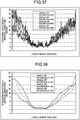
- FIG. 37 illustrates the calculated results. As illustrated in FIG. 37 , each of the standard deviations of the noise signal strengths increases toward ends in the longitudinal direction. Since variations depending on the position in the width direction were large, moving average filtering was applied to waveforms illustrated in FIG. 37 to smooth the waveforms. As a result, as illustrated in FIG. 38 , the standard deviation of the noise signal strength has the smallest value of approximately 2 at the center portion, and the standard deviation of the noise signal strength increases toward the ends.
- the signal strength of a surface defect to be detected is approximately 15. Therefore, to ensure an S/N ratio of 3 or higher at which detection can be made, the standard deviation of the noise signal strength needs to be 5 or smaller.
- the light projecting/receiving difference ⁇ refers to a value that is represented by Expression (18) given below using the angle of incidence ⁇ of the illumination light into the defect position and the angle of reflection ⁇ in the inspection target portion, and that indicates how the projecting/receiving angles of the illumination light are closer to or farther from the specular reflection direction than in the case where the test sample center Sc is irradiated.
- FIGS. 39 and 40 illustrate the calculated results.
- FIG. 39 is a diagram illustrating changes in the light projecting/receiving difference ⁇ on the near side and the far side with respect to the change in angle of incidence of the illumination light at an end of the range in which the standard deviation of the noise signal strength is 5 or smaller.
- FIG. 40 is a diagram illustrating a change in the absolute value of the difference between a light projecting/receiving difference ⁇ 1 on the near side and a light projecting/receiving difference ⁇ 2 on the far side with respect to the change in angle of incidence of the illumination light at the end of the range in which the standard deviation of the noise signal strength is 5 or smaller.
- the light projecting/receiving differences ⁇ 1 and ⁇ 2 on the near side and the far side change with the angle of incidence of the illumination light.
- of the difference between the light projecting/receiving difference ⁇ 1 on the near side and the light projecting/receiving difference ⁇ 2 on the far side is larger than 22° regardless of the angle of incidence of the illumination light.
- the standard deviation of the noise signal strength can be said to be 5 or smaller if the absolute value
- ⁇ ⁇ ⁇ ⁇ + ⁇
- ⁇ 1 is represented using the vectors a 1 and b 1
- ⁇ 2 is represented using the vectors a 2 and b 2
- the steel product is a thick steel plate in the description above
- the present invention is also applicable to a thin steel sheet.
- ⁇ represents an inner product
- represents a norm.
- the illumination light beam is emitted from the width direction of the thick steel plate, and in the other case, the illumination light beam is emitted from the longitudinal direction of the thick steel plate.
- the longitudinal directional field of view per one area sensor can be designed in any manner by designing the capturing period in accordance with the moving speed of the thick steel plate.
- the optical system is preferably designed so as to satisfy the condition represented by Expression (1) only when the illumination light beam is emitted from the longitudinal direction of the thick steel plate among the two directions of the width direction and the longitudinal direction of the thick steel plate, in other words, only when the irradiation direction of one illumination light beam of illumination light beams emitted from two light sources is parallel to the longitudinal direction of the steel product, and the illumination light beam is preferably supplementarily used when emitted from the width direction of the thick steel plate. Due to this, the inspection can be conducted with an optimal optical system while reducing the cost.
- FIG. 41 is a schematic diagram illustrating the configuration of the optical system used in the experiment. The same elements as those in FIG. 35 are assigned with the same reference signs.
- the positional relation of the area sensor 4, the two light sources 2, the test sample (thick steel plate) S, and the test sample center Sc is the same as that in FIG. 35 .
- the angle of incidence ⁇ of the illumination light beams is 70°
- the resolution of the area sensor was 1.0 mm/pixel
- the inspection range was 350 mm ⁇ 270 mm.
- FIG. 42 illustrates a detection result of the surface defect. As illustrated in (d) of FIG.
- an image of the surface defect portion has a brightness pattern, and the surface defect is detectable.
- the detection result of the surface defect represents a portion where a bright portion and a dark portion were expanded and overlapped, where the threshold of the signal strength was set to 15.
- FIGS. 43(a) to 43(c) are diagrams illustrating detection results of a surface defect called a burr-pressed mark that is long in the longitudinal direction.
- the signal strength was very small when the illumination light was emitted from the longitudinal direction of the thick steel plate.
- the brightness pattern could be surely seen when the illumination light was emitted from the width direction of the thick steel plate.
- FIG. 44 is a diagram illustrating a result of inspection of a surface defect obtained by reducing the field of view in only the longitudinal direction of a thick steel plate.
- the inspection target was a steel plate having poor surface characteristics. As illustrated in FIG. 44 , it has been found that positions with unevenly balanced projecting/receiving angles of the illumination light serve as a noise factor, and that limiting the inspection range allows the inspection to be conducted in the condition of well-balanced projecting/receiving angles.
- a surface defect of a steel product may be detected using the surface defect detection method according to the present invention, and the steel product may be manufactured on the basis of the detection result.
- the present invention is not limited to the description and the drawings that constitute a part of the disclosure of the present invention according to the present embodiment.
- a surface defect of a steel product may be detected using the surface defect detection method according to the present invention, and the steel product may be manufactured on the basis of the detection result.
- other embodiments, examples, operational techniques, and the like made by those skilled in the art on the basis of the present embodiment are all included in the scope of the present invention.
- the present invention can provide a surface defect detection device and a surface defect detection method that enable accurate distinction of scale or harmless patterns from surface defects.
- the present invention can also provide a method for manufacturing a steel product, the method enabling the accurate distinction of the scale or the harmless patterns from the surface defects, and enabling manufacturing of the steel product on the basis of the distinction result.
Landscapes
- Physics & Mathematics (AREA)
- Health & Medical Sciences (AREA)
- Life Sciences & Earth Sciences (AREA)
- Chemical & Material Sciences (AREA)
- Analytical Chemistry (AREA)
- Biochemistry (AREA)
- General Health & Medical Sciences (AREA)
- General Physics & Mathematics (AREA)
- Immunology (AREA)
- Pathology (AREA)
- Engineering & Computer Science (AREA)
- Textile Engineering (AREA)
- Investigating Materials By The Use Of Optical Means Adapted For Particular Applications (AREA)
Abstract
Description
- The present invention relates to a surface defect detection device and a surface defect detection method that optically detect surface defects of a steel product, and to a method for manufacturing a steel product, the method detecting surface defects of the steel product using the surface defect detection method, and manufacturing the steel product on the basis of the detection results.
- In recent years, from the viewpoint of improving yield by preventing mass incompatibility, it is desired that, in manufacturing processes of steel products, surface defects of a steel product are detected in hot or cold conditions. The term "steel product" as used herein refers to an article of iron or steel, such a steel sheet or a shaped steel, including, for example, a seamless steel pipe, a welded steel pipe, a hot-rolled steel sheet, a cold-rolled steel sheet, and a thick plate, and to a semifinished product, such as a slab, produced in the process of manufacturing the article of iron or steel. For this reason, as a method for detecting the surface defects of the steel product, a method has been developed in which a billet in the manufacturing process of a seamless steel pipe is irradiated with light, light reflected therefrom is received, and a determination is made on the basis of the light quantity of the reflected light as to whether a surface defect is present (refer to Patent Literature 1). A method has also been developed in which visible light beams in a plurality of wavelength regions that neither affect nor are affected by self-emitting light emitted from a hot steel product and do not affect each other are emitted from mutually symmetrical directions oblique to a normal line to the surface of the hot steel product, an image formed by combined reflected light beams and images formed by the individual reflected light beams are obtained in the normal direction to the surface of the hot steel product, and a surface defect of the hot steel product is detected from a combination of these images (refer to Patent Literature 2).
-
- Patent Literature 1: Japanese Laid-open Patent Publication No.
11-037949 - Patent Literature 2: Japanese Laid-open Patent Publication No.
59-052735 - According to the method described in
Patent Literature 1, since harmless patterns and scale have different reflectance from that of a base steel portion, the sound harmless patterns or scale may be erroneously detected as the surface defects. For this reason, in the method described inPatent Literature 1, the billet is distinguished from the scale using the fact that the shape of the billet is linear. However, the surface defects of a steel product have not only linear shapes, but also various shapes, such as circular shapes. Therefore, the method described inPatent Literature 1 is difficult to be applied to the detection processing for the surface defects of the steel product. In the method described inPatent Literature 2, since a large number of types of surface defects, scale, harmless patterns and the like are present, simply combining the images is difficult to distinguish the surface defects from the scale or the harmless patterns.
In addition, detection logic for dealing with a combination of a large number of images is realistically difficult to be established. - The present invention has been made in view of the above described problems, and an object thereof is to provide a surface defect detection device and a surface defect detection method that enable accurate distinction of the scale or the harmless patterns from the surface defects. Another object of the present invention is to provide a method for manufacturing a steel product, the method enabling the accurate distinction of the scale or the harmless patterns from the surface defects, and enabling manufacturing of the steel product on the basis of the distinction result.
- To solve the problem and achieve the object, a surface defect detection device to optically detect a surface defect of a steel product according to the present invention includes: an irradiation unit configured to irradiate a same inspection target portion with illumination light beams from different directions using two or more distinguishable light sources; and a detection unit configured to acquire images formed by reflected light beams of the respective illumination light beams, and to detect the surface defect in the inspection target portion by performing difference processing between the acquired images, wherein a vector a1, a vector b1, a vector a2, and a vector b2 satisfy Expression (1) given below in the inspection target portion:

a1 denotes a vector representing a specular reflection direction of an illumination light beam incident from one light source of two light sources into the inspection target portion, b1 denotes a vector in the inspection target portion representing a reflection direction of the illumination light beam incident from the one light source toward a photographing unit configured to photograph the images, a2 denotes a vector representing a specular reflection direction of an illumination light beam incident from the other light source of the two light sources into the inspection target portion, and b2 denotes a vector in the inspection target portion representing a reflection direction of the illumination light beam incident from the other light source toward the photographing unit configured to photograph the images. - Moreover, in the surface defect detection device according to the present invention, an irradiation direction of one illumination light beam of the illumination light beams emitted from the two light sources is parallel to a longitudinal direction of the steel product.
- Moreover, a surface defect detection method to optically detect a surface defect of a steel product according to the present invention includes: an irradiation step of irradiating a same inspection target portion with illumination light beams from different directions using two or more distinguishable light sources; and a detection step of acquiring images formed by reflected light beams of the respective illumination light beams, and detecting the surface defect in the inspection target portion by performing difference processing between the acquired images, wherein a vector a1, a vector b1, a vector a2, and a vector b2 satisfy Expression (1) given below in the inspection target portion:

a1 denotes a vector representing a specular reflection direction of an illumination light beam incident from one light source of two light sources into the inspection target portion, b1 denotes a vector in the inspection target portion representing a reflection direction of the illumination light beam incident from the one light source toward a photographing unit configured to photograph the images, a2 denotes a vector representing a specular reflection direction of an illumination light beam incident from the other light source of the two light sources into the inspection target portion, and b2 denotes a vector in the inspection target portion representing a reflection direction of the illumination light beam incident from the other light source toward the photographing unit configured to photograph the images. - Moreover, in the surface defect detection method according to the present invention, an irradiation direction of one illumination light beam of the illumination light beams emitted from the two light sources is parallel to a longitudinal direction of the steel product.
- Moreover, in the surface defect detection method according to the present invention, the irradiation step includes a step of emitting the illumination light beams by repeatedly emitting light from two or more flash light sources such that light emitting times of the flash light sources do not overlap each other, and/or a step of simultaneously emitting illumination light beams of two or more light sources having wavelength ranges not overlapping one another, and in the case of simultaneously emitting the illumination light beams of the two or more light sources having wavelength ranges not overlapping one another, the detection step includes a step of acquiring the images formed by the reflected light beams of the respective illumination light beams by separating the reflected light beams of the respective mixed illumination light beams using filters configured to transmit light beams having the same wavelengths as wavelengths of the illumination light beams.
- Moreover, in the surface defect detection method according to the present invention, the detection step includes a first determination step of extracting a bright portion and a dark portion of an image obtained by performing the difference processing between the acquired images, and determining presence or absence of a concavo-convex surface defect based on a positional relation between the bright portion and the dark portion thus extracted and irradiation directions of the illumination light beams.
- Moreover, a method for manufacturing a steel product according to the present invention includes: a step of detecting a surface defect of the steel product using the surface defect detection method according to the present invention; and manufacturing the steel product based on a result of the detection.
- A surface defect detection device and a surface defect detection method according to the present invention can accurately distinguish scale or harmless patterns from surface defects. A method for manufacturing a steel product according to the present invention enables the accurate distinction of the scale or the harmless patterns from the surface defects, and enables manufacturing of the steel product on the basis of the distinction result.
-
-
FIG. 1 is a schematic diagram illustrating a configuration of a surface defect detection device serving as a first embodiment of the present invention. -
FIG. 2 is a schematic diagram illustrating a configuration of a modification of area sensors illustrated inFIG. 1 . -
FIG. 3 is a timing diagram illustrating drive timing of light sources and the area sensors illustrated inFIG. 1 . -
FIG. 4 is a diagram illustrating examples of two two-dimensional images obtained by photographing a surface defect and scale and a harmless pattern, and a difference image therebetween. -
FIG. 5 is a schematic diagram illustrating a configuration of a device used in an experiment for investigating a relation between an angle of incidence of illumination light and reflectance of a sound portion (base steel portion). -
FIG. 6 is a diagram illustrating a relation between an angle of incidence of laser and a light quantity received by a power meter. -
FIG. 7 is a schematic diagram for explaining surface defect detection processing serving as a second mode of the present invention. -
FIG. 8 is a schematic diagram for explaining surface defect detection processing serving as a third mode of the present invention. -
FIG. 9 is a schematic diagram illustrating a configuration of a device used in an example. -
FIG. 10 is a diagram illustrating results of surface defect detection processing of the example. -
FIG. 11 is a diagram illustrating results of surface defect detection processing for a steel pipe portion where scale has been generated. -
FIG. 12 is a schematic diagram illustrating a configuration of a modification of the surface defect detection device serving as the first embodiment of the present invention. -
FIG. 13 is a schematic diagram illustrating a configuration of another modification of the surface defect detection device serving as the first embodiment of the present invention. -
FIG. 14 depicts diagrams illustrating shades and shadows when the illumination light is emitted from either side in cases where the surface shape of an inspection target portion is concave and convex. -
FIG. 15 is a diagram illustrating an example of a difference image of a concave surface defect. -
FIG. 16 is a flowchart illustrating a flow of a method for calculating a positional relation between a bright portion and a dark portion using expansion processing. -
FIGS. 17(a) and 17(b) are diagrams illustrating an example of a difference image and a one-dimensional profile of a brightness pattern thereof. -
FIGS. 18(a) and 18(b) are diagrams illustrating an example of a two-dimensional image and a one-dimensional profile of a filter. -
FIGS. 19(a) and 19(b) are diagrams illustrating an example of a difference image having been subjected to filtering using the filter illustrated inFIGS. 18(a) and 18(b) , and a one-dimensional profile thereof. -
FIG. 20 is a schematic diagram illustrating a modification of arrangement positions of the light sources. -
FIG. 21 depicts schematic diagrams illustrating brightness patterns obtained according to the arrangement positions of the light sources illustrated inFIG. 20 . -
FIG. 22 is a diagram illustrating results of surface defect detection processing of an example. -
FIG. 23 is a diagram illustrating a difference image of a dent flaw. -
FIGS. 24(a) and 24(b) are diagrams illustrating difference images of a roll mark when the illumination light is emitted from the width direction and the longitudinal direction of a thick steel plate. -
FIGS. 25(a) and 25(b) are diagrams illustrating inclinations of a surface defect when the illumination light is emitted from the width direction and the longitudinal direction of the thick steel plate. -
FIG. 26 is a diagram illustrating an inclination of a sound portion when the illumination light is emitted from the width direction of the thick steel plate. -
FIG. 27 is a diagram illustrating a configuration of a two-dimensional model of an optical system. -
FIG. 28 is a diagram illustrating a fitting result of an image profile to a theoretical curve. -
FIG. 29 is a diagram illustrating a configuration of the optical system. -
FIG. 30 is a diagram illustrating changes in signal strength with a change in slope angle of a surface defect when the angle of incidence of the illumination light is 45°, 60°, and 75°. -
FIGS. 31(a) and 31(b) are diagrams illustrating reflection models of the illumination light on a sound portion surface and a highly diffusive surface. -
FIGS. 32(a) to 32(c) are diagrams illustrating difference images of a surface defect portion. -
FIGS. 33(a) and 33(b) are diagrams illustrating images obtained when the illumination light is emitted from a right side direction and a left side direction to a thick steel plate with a surface without concavity and convexity to which highly diffusive scale is attached. -
FIGS. 34(a) to 34(c) are diagrams illustrating an image obtained when the illumination light is emitted from the right side direction, an image obtained when the illumination light is emitted from the left side direction, and a difference image therebetween. -
FIG. 35 is a diagram illustrating a configuration of an optical system. -
FIG. 36 is a diagram illustrating a change in difference image with a change in angle of incidence of the illumination light. -
FIG. 37 is a diagram illustrating standard deviations of noise signal strengths in longitudinal positions before moving average filtering is applied. -
FIG. 38 is a diagram illustrating the standard deviations of the noise signal strengths in the longitudinal positions after the moving average filtering is applied. -
FIG. 39 is a diagram illustrating relations of the angle of incidence of the illumination light with light emission/reception differences on the near side and the far side. -
FIG. 40 is a diagram illustrating a relation between the angle of incidence of the illumination light and the absolute value of the difference between the light emission/reception difference on the near side and the light emission/reception difference on the far side. -
FIG. 41 is a diagram illustrating a configuration of an optical system. -
FIG. 42 depicts diagrams illustrating a detection result of a surface defect. -
FIGS. 43(a) to 43(c) are diagrams illustrating detection results of a burr-pressed mark. -
FIG. 44 is a diagram illustrating a result of inspection of a surface defect obtained by reducing the field of view in only the longitudinal direction of a thick steel plate. - The following describes configurations and operations of surface defect detection devices serving as first to third embodiments of the present invention with reference to the drawings.
- First, the configuration and operations of a surface defect detection device serving as the first embodiment of the present invention will be described with reference to
FIGS. 1 to 13 . -
FIG. 1 is a schematic diagram illustrating the configuration of the surface defect detection device serving as the first embodiment of the present invention. As illustrated inFIG. 1 , this surfacedefect detection device 1 serving as the first embodiment of the present invention is a device that detects a surface defect of a cylindrical steel pipe P conveyed in the direction of the arrow inFIG. 1 , and includes, as main components,light sources function generator 3,area sensors image processing device 5, and amonitor 6. - The
light sources function generator 3. Thelight sources light sources - The
area sensors light sources function generator 3. Thearea sensors image processing device 5. Thearea sensors respective area sensors - To solve a positioning problem, the
area sensors FIG. 2 , the optical axes of thearea sensors semitransparent mirror 10, a beam splitter, and a prism. Due to this, a difference image to be described later can be accurately acquired. - The
image processing device 5 is a device that detects a surface defect in the inspection target portion by performing the difference processing (to be described later) between the two two-dimensional images received from thearea sensors image processing device 5 outputs the two-dimensional images received from thearea sensors monitor 6. - The surface
defect detection device 1 having the configuration described above distinguishes the scale or the harmless pattern from the surface defect in the inspection target portion by performing surface defect detection processing to be described below. The surface defect as mentioned herein refers to a concavo-convex defect. The scale or the harmless pattern refers to a portion having a surface film or surface characteristics with optical characteristics different from those of a base steel portion with a thickness of roughly several micrometers to several tens of micrometers, and is a portion causing noise in the surface defect detection processing. The following describes surface defect detection processing serving as first to third modes of the present invention. - First, the surface defect detection processing serving as the first mode of the present invention will be described with reference to
FIGS. 3 to 6 . -
FIG. 3 is a timing diagram illustrating drive timing of thelight sources area sensors FIG. 3 , d denotes a light-emitting time of thelight sources area sensors light sources light sources - That is, as illustrated in
FIG. 3 , in the present mode, first, thefunction generator 3 transmits a trigger signal to thelight source 2a and thearea sensor 4a, thelight source 2a emits one of the illumination light beams L, and thearea sensor 4a completes the photographing of a two-dimensional image within the time d. After thearea sensor 4a has completed the photographing of the two-dimensional image, thefunction generator 3 transmits a trigger signal to thelight source 2b and thearea sensor 4b, and a two-dimensional image is photographed in the same manner. According to present mode, the two-dimensional images formed by the individual reflected light beams corresponding to the illumination light beams L emitted from the respective light sources can be photographed with the time difference d without a reduction in light quantity. - If the conveyance speed of the steel pipe P is high, the light-emitting time d of the flash light sources is preferably short. This is because reducing the light-emitting time d reduces a shutter delay between the two two-dimensional images obtained by the
area sensors 
- If the size of a surface defect to be detected is, for example, 20 mm, signals of at least 5×5 pixels are empirically required for detecting the surface defect. Therefore, only a resolution of 4 mm/pixel is needed. In this case, the allowable amount of the positional displacement caused by the light emission timing of the illumination light beams L empirically needs to be within 0.2 pixels. Therefore, if the conveyance speed of the steel pipe P is 1 m/s, 3 m/s, or 5 m/s, the light-emitting time of the
light sources - In the present mode, after applying image processing, such as calibration, shading correction, and denoising, to the two-dimensional images received from the
area sensors image processing device 5 detects the surface defect in the inspection target portion by performing the difference processing between the two-dimensional images. - Specifically, letting Ia(x,y) denote a luminance value of each pixel constituting a two-dimensional image Ia obtained when the illumination light beams L is emitted from the
light source 2a (where the number of pixels is X × Y, the x-coordinate satisfies 1 ≤ x ≤ X, and the y-coordinate satisfies 1 ≤ y ≤ Y), and Ib(x,y) denote a luminance value of each pixel constituting a two-dimensional image Ib obtained when the illumination light beam L is emitted from thelight source 2b, a luminance value I_diff(x,y) of each pixel of a difference image I_diff therebetween is represented by Expression (3) given below.
-
FIG. 4 illustrates examples of the two-dimensional images Ia and Ib obtained by photographing the surface defect, and the scale and the harmless pattern that are not defects, and the difference image I_diff therebetween, in (a), (b), and (c), respectively. As illustrated in (a), (b), and (c) inFIG. 4 , in the sound portion, an angle formed between the normal vector and thelight source 2a equals an angle formed between the normal vector and thelight source 2b regardless of the scale or the harmless pattern, and consequently, the luminance value Ia(x,y) = the luminance value Ib(x,y), that is, the luminance value I_diff(x,y) = 0. In the surface defect portion, however, the surface has a concavo-convex shape. As a result, a portion is always present where the angle formed between the normal vector and thelight source 2a does not equal the angle formed between the normal vector and thelight source 2b, and consequently, the luminance value Ia(x,y) # the luminance value Ib(x,y), that is, the luminance value I_diff(x,y) # 0. - Consequently, by generating the difference image between the two two-dimensional images using a
subtractor 11, the scale and the harmless pattern that are not defects are removed, and the surface defect alone can be detected. The surface defect alone is detected in this manner; a final evaluation is made on the basis of various feature quantities as to whether the surface defect is harmful; and the evaluation result is displayed on themonitor 6. - If a positional displacement is present between the two two-dimensional images which affects the difference image, a two-dimensional low pass filter is preferably used to reduce the influence of the positional displacement between the two-dimensional images. In this case, let H denote the two-dimensional low-pass filter, then a luminance value I'_diff(x,y) of the difference image is represented by Expression (4) given below.

- The
light sources - The angle of incidence of the illumination light beams L is preferably in a range preventing a specular reflection component from being included in reflected light from the sound portion and enabling ensuring of a sufficient light quantity. The inventors of the present invention conducted an experiment to investigate a relation between the angle of incidence of the illumination light beams L and reflectance of the sound portion (base steel portion).
FIG. 5 illustrates the configuration of a device used in the experiment. As illustrated inFIG. 5 , in this experiment, apower meter 12 was fixed in a position on anormal vector 1 of a target position on a surface of aslab sample 14. The light quantity received by thepower meter 12 was measured while an angle of incidence θ of alaser 13 relative to the normal vector l was varied from 0° to 90°.FIG. 6 illustrates results of the experiment. As illustrated inFIG. 6 , when the angle of incidence θ is in a range of 0° to 20°, the light quantity received by thepower meter 12 is large due to inclusion of the specular reflection component, but, when the angle of incidence θ is 60° or larger, the light quantity received by thepower meter 12 greatly drops. Therefore, the light quantity received can be increased by reducing the angle of incidence of the illumination light beams L unless any problem occurs in detectivity. - The resolution in the depth direction of the inspection target portion depends on the inclination angle of the defect and resolutions of the
area sensors - The following describes the surface defect detection processing serving as the second mode of the present invention with reference to
FIG. 7 . - In the surface defect detection processing serving as the second mode of the present invention, the
light sources light sources FIG. 7 , two types ofwavelength selection filters light sources area sensors - Such a configuration causes the reflected light beam of the illumination light beam L from the
light source 2a to be received by only thearea sensor 4a through thewavelength selection filters light source 2b to be received by only thearea sensor 4b through the wavelength selection filters 20b and 21b. Consequently, by matching the photographing timing of thearea sensors light sources - If the moving speed of the inspection target portion is high, to prevent the positional displacement caused by the movement of the inspection target portion, the
light sources light sources wavelength selection filter 20a, a green color transmitting filter is used as thewavelength selection filter 20b, and the two-dimensional images are photographed using one color camera so that only the reflected light beam of the illumination light beam L from thelight source 2a is received in the blue channel, and only the reflected light beam of the illumination light beam L from thelight source 2b is received in the green channel. - The following describes the surface defect detection processing serving as the third mode of the present invention with reference to
FIG. 8 . - In the surface defect detection processing serving as the third mode of the present invention, the
light sources light sources FIG. 8 , linearpolarizing plates light sources polarizing plates polarizing plates area sensors - Such a configuration causes the reflected light beam of the illumination light beam L from the
light source 2a to be received by only thearea sensor 4a, and causes the reflected light beam of the illumination light beam L from thelight source 2b to be received by only thearea sensor 4b. Consequently, by matching the photographing timing of thearea sensors - If the moving speed of the inspection target portion is high, the
light sources light sources - In this example, as illustrated in
FIG. 9 , the surface defect of the steel pipe P was detected using a method of using the flash light sources as thelight sources light sources area sensors FIG. 10 illustrates results of the surface defect detection processing. Part (a) inFIG. 10 illustrates a two-dimensional image obtained when the illumination light beam L is emitted from thelight source 2a; part (b) inFIG. 10 illustrates a two-dimensional image obtained when the illumination light beam L is emitted from thelight source 2b; and part (c) inFIG. 10 illustrates a difference image between the two-dimensional image illustrated in part (a) ofFIG. 10 and the two-dimensional image illustrated in part (b) ofFIG. 10 . Signal-to-noise (S/N) ratios of the images illustrated in parts (a) to (c) ofFIG. 10 were 3.5, 3.5, and 6.0, in that order. Thus, the S/N ratio of the difference image was improved from those in the cases in each of which the illumination light beam L was simply emitted from one direction. -
FIG. 11 is a diagram illustrating results of the surface defect detection processing for a steel pipe portion where scale has been generated. Part (a) inFIG. 11 illustrates a two-dimensional image obtained when the illumination light beam L is emitted from thelight source 2a; part (b) inFIG. 11 illustrates a two-dimensional image obtained when the illumination light beam L is emitted from thelight source 2b; and part (c) inFIG. 11 illustrates a difference image between the two-dimensional image illustrated in part (a) ofFIG. 11 and the two-dimensional image illustrated in part (b) ofFIG. 11 . Black spots spreading over the whole two-dimensional images illustrated in parts (a) and (b) inFIG. 11 are the scale serving as noise. Since the scale had a flat shape, the image of the scale was removed by acquiring the difference image. In the difference image, the signal of the scale serving as the noise was reduced to a quarter of a case where the illumination light beam L was simply emitted from one direction. -
FIG. 12 is a schematic diagram illustrating the configuration of a modification of the surface defect detection device serving as the first embodiment of the present invention. As illustrated inFIG. 12 , in the present modification, illumination light emitted from the singlelight source 2a is divided by a plurality ofmirrors wavelength selection filters polarizing plates -
FIG. 13 is a schematic diagram illustrating the configuration of another modification of the surface defect detection device serving as the first embodiment of the present invention. As illustrated inFIG. 13 , in the present modification, instead of limiting the wavelengths of the light sources using thewavelength selection filters FIG. 7 , the wavelengths of light sources are limited usingpulse lasers diffusion plates pulse lasers pulse lasers diffusion plates - In the present modification, a dichroic mirror is used instead of the
wavelength selection filters area sensors FIG. 7 . The dichroic mirror refers to a mirror that reflects light having a particular wavelength component and transmits light having the other wavelength components. Using the dichroic mirror eliminates the necessity of the wavelength selection filters. Although the illumination light is emitted from two directions in the present modification, the same applies to a case where illumination light is emitted from three or more directions. - The following describes the configuration and operations of a surface defect detection device serving as the second embodiment of the present invention with reference to
FIGS. 14 to 22 . The configuration of the surface defect detection device of the present embodiment is the same as the configuration of the surface defect detection device of the above described first embodiment. Thus, the following omits the description of the configuration, and describes only the operations of the surface defect detection device. - The surface
defect detection device 1 serving as the second embodiment of the present invention distinguishes scale or a harmless pattern from a concavo-convex surface defect in the inspection target portion by performing surface defect detection processing to be described below. The scale or the harmless pattern refers to a portion having a surface film or surface characteristics with optical characteristics different from those of a base steel portion with a thickness of roughly several micrometers to several tens of micrometers, and is a portion causing noise in the surface defect detection processing. - In the surface defect detection processing serving as the second embodiment of the present invention, after applying image processing, such as calibration, shading correction, and denoising, to the two two-dimensional images received from the
area sensors image processing device 5 generates the difference image by performing difference processing between the two-dimensional images, and detects the concavo-convex surface defect in the inspection target portion from the generated difference image. - Specifically, let Ia(x,y) denote a luminance value of each pixel constituting the two-dimensional image Ia obtained when the illumination light beams L is emitted from the
light source 2a (where the number of pixels is X × Y, the x-coordinate satisfies 1 ≤ x ≤ X, and the γ-coordinate satisfies 1 ≤ y ≤ Y), and Ib(x,y) denote a luminance value of each pixel constituting the two-dimensional image Ib obtained when the illumination light beam L is emitted from thelight source 2b, then the luminance value I_diff(x,y) of each pixel of the difference image I_diff obtained by the difference processing is represented by Expression (3), which is already given. - As illustrated in
FIG. 4 , in the sound portion, the angle formed between the normal vector of the surface and thelight source 2a equals the angle formed between the normal vector of the surface and thelight source 2b regardless of presence or absence of the scale or the harmless pattern, and consequently, the luminance value Ia(x,y) = the luminance value Ib(x,y), that is, the luminance value I_diff(x,y) = 0. In a concavo-convex surface defect portion, however, the surface has a concavo-convex shape. As a result, a portion is always present where the angle formed between the normal vector of the surface and thelight source 2a does not equal the angle formed between the normal vector of the surface and thelight source 2b, and consequently, the luminance value Ia(x,y) # the luminance value Ib(x,y), that is, the luminance value I_diff(x,y) # 0. Consequently, by generating the difference image I_diff between the two two-dimensional images using thesubtractor 11, an image of the scale or the harmless pattern that is sound and not a surface defect can be removed. - The following describes logic for detecting the concavo-convex surface defect from the difference image I_diff. Parts (a) and (b) in
FIG. 14 depict diagrams illustrating shades and shadows when the illumination light is emitted from either of the light sources to the inspection target portion in cases where the surface shape of an inspection target portion is concave and convex, respectively. As illustrated in (a) ofFIG. 14 , if the surface shape of the inspection target portion is concave, the near side of the light source is darker due to reduction in light quantity of the illumination light, and the far side of light source is brighter because of being closer to a specular reflection direction. In contrast, as illustrated in (b) ofFIG. 14 , if the surface shape of the inspection target portion is convex, the near side of the light source is brighter because of being closer to a specular reflection direction, and the far side of light source is darker because of being shaded by the convex shape. - That is, the brightness pattern of the reflected light beam of the illumination light beam differs between the case where the surface shape of the inspection target portion is concave and the case where the surface shape thereof is convex. Therefore, presence or absence of a concavo-convex surface defect can be detected by recognizing the brightness pattern of the reflected light beam. Thus, the following describes a method for detecting a concavo-convex surface defect by recognizing the brightness pattern of the reflected light beam. Hereinafter, of concavo-convex surface defects, a concave surface defect is detected. However, a convex surface defect can be detected using the same logic. A bright portion to be mentioned below refers to a blob that is obtained by performing connection processing of pixels having luminance of a predetermined threshold or higher in the difference image I_diff and that has an area equal to or larger than a predetermined value. A dark portion to be mentioned below refers to a blob that is obtained by performing the connection processing of pixels having luminance of a predetermined threshold or lower in the difference image I_diff and that has an area equal to or larger than a predetermined value. The blob refers to a collection of labeled pixels.
- In the present embodiment, the brightness pattern is recognized by extracting the bright portion and the dark portion by performing threshold processing. Specifically, in the surface
defect detection device 1 of the present embodiment, thelight sources FIG. 15 . When images of the bright and the dark portions are binarized using luminance thresholds The and -The, binarized images I_blight and I_dark of the bright and the dark portions, respectively, are represented by Expression (5) given below.
- The images of the bright and the dark portions are binarized in this manner, and are subjected to connection and isolated point removal as needed. Then, the positional relation between the bright and the dark portions is calculated to detect the presence or absence of a concavo-convex surface defect. Various methods are available as a method for calculating the positional relation between the bright and the dark portions. The following describes three representative calculation methods, but other calculation methods may be used as long as the other methods are capable of calculating the positional relation between the bright and the dark portions.
- A first positional relation calculation method is a method for calculating the positional relation between the bright and the dark portions by applying expansion processing in a certain direction to the bright and the dark portions.
FIG. 16 illustrates the flowchart of this calculation method. Since a concave surface defect is detected in the present embodiment, a case will be described where a brightness pattern with the right side being bright and the left side being dark is recognized. The expression "the right side being bright and the left side being dark" means that the dark portion is always present on the left side of the bright portion, and the bright portion is always present on the right side of the dark portion. Hence, in this calculation method, first, theimage processing device 5 applies the expansion processing in the rightward direction to the dark portion, and applies the expansion processing in the leftward direction to the bright portion (Steps S1a and S1b). Let I_blight_extend and I_dark_extend denote images of the bright and the dark portions, respectively, and W denote an expansion length, then the expansion processing is expressed by Expression (6) given below. In Expression (6), assuming the upper left corner of the two-dimensional image to be the origin, the downward direction is assumed to be positive in the y-axis direction, and the rightward direction is assumed to be positive in the x-axis direction.
- In the present embodiment, the bright and the dark portions are expanded by the same length W. The expansion length W, however, need not be the same for both the bright and the dark portions. As an extreme case, the expansion processing may be applied to only one of the bright and the dark portions. The expansion length W also depends on the size of the surface defect desired to be detected.
- Then, the
image processing device 5 performs AND processing on the images I_blight_extend and I_dark_extend of the bright and the dark portions that have been subjected to the expansion processing as represented by Expression (7) given below, and thereby extracts, as a defect candidate portion image I_defect, an overlapping portion between the images I_blight_extend and I_dark_extend of the bright and the dark portions that have been subjected to the expansion processing (Steps S2a and S2b) .
- Then, after applying the connection and isolated point removal processing as needed to each of the obtained defect candidate portion images I_defect, the
image processing device 5 performs labeling processing to generate a defect candidate blob I_defect_blob (Step S3). Theimage processing device 5 extracts feature quantities of each of the defect candidate blobs I_defect_blob, and determines, on the basis of the extracted results, whether each of the defect candidate blobs I_defect_blob is a concave surface defect (Steps S4a and S4b). Since information on the bright and the dark portions is needed to investigate the feature quantities of the defect candidate blob I_defect_blob, the bright and the dark portions are restored from the defect candidate blob I_defect_blob. - Specifically, a bright portion is always present on the right side of a defect candidate portion, and a dark portion is always present on the left side thereof. Hence, the
image processing device 5 searches the defect candidate blob I_defect_blob starting from the centroid thereof toward the left side thereof for the dark portion binarized image I_dark, and regards the first found blob as a dark portion defect candidate blob I_dark_blob. In the same manner, theimage processing device 5 searches the defect candidate blob I_defect_blob starting from the centroid thereof toward the right side thereof for the bright portion binarized image I_blight, and regards the first found blob as a bright portion defect candidate blob I_blight_blob. Theimage processing device 5 extracts feature quantities from the bright portion defect candidate blob I_blight_blob and the dark portion defect candidate blob I_dark_blob that have been restored as described above, and determines, on the basis of the extracted feature quantities, whether each of the defect candidate blobs I_defect_blob is a concave surface defect. Specific feature quantities differ depending on the defect, and thus will not be described here, but one example will be given in an example to be described later. - In a second positional relation calculation method, after the above-described threshold processing is performed and the connection and isolated point removal processing is performed as needed, the bright and the dark portions are extracted and subjected to labeling, and the positional relation between the bright and the dark portions is recognized so as to detect the concave surface defect. Specifically, first, the
image processing device 5 individually recognizes the bright and the dark portions by the labeling, and obtains centroid information on the bright and the dark portions. Theimage processing device 5 then determines, on the basis of the centroid information on the bright and the dark portions, whether the centroid of the dark portion is present in a predetermined range on the right side of each bright portion. If the centroid of the dark portion is present, theimage processing device 5 recognizes a combination of the bright and the dark portions forming a pair as a brightness pattern, and performs a feature quantity analysis of the brightness pattern to determine whether the brightness pattern is a concave surface defect. Although the brightness pattern is recognized using the centroid information here, the information used for the recognition of the brightness pattern need not be the centroid information as long as the positions of the bright and the dark portions can be obtained using the information (such as upper end positions or lower end positions thereof). - In a third positional relation calculation method, the concave surface defect is detected by recognizing the brightness pattern using a filter without performing the above-described threshold processing. Specifically, in the surface
defect detection device 1 illustrated inFIG. 1 , since thelight sources FIGS. 17(a) and 17(b) are diagrams respectively illustrating an example of a difference image and a one-dimensional profile of a brightness pattern on a line segment L4 illustrated inFIG. 17(a) . - As illustrated in
FIGS. 17(a) and 17(b) , since the right side is bright and the left side is dark in the concave surface defect, the one-dimensional profile of the brightness pattern is a characteristic one-dimensional profile in which the right side is chevron-shaped and the left side is valley-shaped. Hence, in the present embodiment, a filter H with the right side being chevron-shaped and the left side being valley-shaped is generated in advance, and the filter H is applied to the difference image I_diff as represented by Expression (8) below so as to generate a two-dimensional image I_cont in which high-frequency noise is reduced and only the brightness pattern is emphasized.
-
FIGS. 18(a) and 18(b) are diagrams respectively illustrating an example of a two-dimensional image of the filter H generated in advance and a one-dimensional profile in the right-left direction thereof.FIGS. 19(a) and 19(b) are diagrams respectively illustrating an example of a difference image having been subjected to filtering using the filter H illustrated inFIGS. 18(a) and 18(b) , and a one-dimensional profile in the right-left direction thereof. As illustrated inFIGS. 19(a) and 19(b) , it is found that a two-dimensional image is obtained in which high-frequency noise is reduced and only the brightness pattern is emphasized. - As needed, several types of filters having different ranges in the width direction may be prepared in advance so as to be compatible with many surface defect sizes. The
image processing device 5 applies, as needed, the connection and isolated point removal processing to the two-dimensional image in which the brightness pattern is emphasized as described above, and then, extracts the defect candidate portion image I_defect by performing the threshold processing. Theimage processing device 5 detects the concave surface defect by applying the same processing as that of the first positional relation calculation method to the extracted defect candidate portion image I_defect. - As is clear from the description above, in the surface defect detection processing serving as the second embodiment of the present invention, the two
distinguishable light sources - In the present embodiment, the right-left brightness pattern is recognized because the light sources are right-left symmetrically arranged. However, even if the arrangement is not right-left symmetric, but upper-lower symmetric or not symmetric, the concavo-convex surface defect can be detected by the same processing. Specifically, if the light sources are upper-lower symmetrically arranged, the brightness pattern only changes from the right-left direction to the upper-lower direction. Therefore, the same processing can be used to detect the concavo-convex surface defect by rotating the brightness pattern by 90°.
- When the
light sources FIG. 20 , the near side is darker and the far side is brighter if the surface defect is concave, and the near side is brighter and the far side is darker if the surface defect is convex. Specifically, if the surface defect is concave, the two-dimensional image obtained by the illumination light beam from thelight source 2a is as illustrated in (a) ofFIG. 21 , and the two-dimensional image obtained by the illumination light beam from thelight source 2b is as illustrated in (b) ofFIG. 21 . Due to this, the difference image has a brightness pattern with a contrast in a direction from the lower left to the upper right, as illustrated in (c) ofFIG. 21 . Hence, if the brightness pattern is rotated by 45°, the concave surface defect can be detected using the same method as that for the brightness pattern in the right-left direction. In addition, difference images having a plurality of respective patterns can be obtained by using three or more light sources. Thus, accuracy of detection of a surface defect can be further improved. - In the present embodiment, the concavo-convex surface defect is detected in the case where the illumination light beams are emitted from the directions symmetrical with respect to the normal line of the inspection target portion. The irradiation directions of the illumination light beams, however, need not be symmetrical. The surface defect detection processing of the present embodiment is generally applicable to manufacturing lines for steel products regardless of whether they are hot or cold.
- In this example, the surface defect detection processing using the above-described first positional relation calculation method was applied to an inspection target portion where a pit flaw is formed and to a sound inspection target portion where no pit flaw is formed. In this example, a luminance ratio, an area ratio, and degrees of roundness of the bright and the dark portions were calculated as the feature quantities. The degrees of roundness are values obtained by dividing areas of the bright and the dark portions by squares of lengths of circumferences thereof and by normalizing the results, and are used in determining whether shapes of the bright and the dark portions are close to circular shapes. If surface defects are due to the same cause, luminance and areas thereof are unlikely to be significantly different between the right and left signals. Thus, the accuracy of detection of a surface defect is improved by evaluating the right-left balance using the luminance ratio and the area ratio. Since shades and shadows are evaluated, the bright and the dark portions are hardly circular, so that those having nearly circular shapes can be determined to be due to a different cause. Therefore, the degrees of roundness were included in the feature quantities. The areas of the bright and the dark portions were calculated, and only a surface defect having an area of a predetermined value or larger was made detectable.
FIG. 22 illustrates the detection results. As illustrated inFIG. 22 , according to this example, a pit flaw and a sound portion where no pit flaw is formed have been found to be accurately distinguishable from each other. - The following describes a study of the angle of incidence of the illumination light and detectivity of a surface defect in the case of detecting the surface defect on a thick steel plate using a surface defect detection method according to the present invention.
FIG. 23 is a diagram illustrating a result of detecting a surface defect called a dent flaw using the surface defect detection method according to the present invention. As illustrated inFIG. 23 , the dent flaw is found to be surely detectable using a brightness pattern. However, it has been found that, when the illumination light is emitted in the width direction of the thick steel plate, a defect signal of a surface defect called a roll mark can hardly be found because the shape of the roll mark is slender, as illustrated inFIG. 24(a) , but, when the illumination light is emitted in the longitudinal direction of the thick steel plate, the strength of the defect signal increases as illustrated inFIG. 24(b) . - Hence, the inventors of the present invention measured the shape of the surface defect, and calculated the inclination of the surface defect when the illumination light was emitted from the width direction of the thick steel plate and when the illumination light was emitted from the longitudinal direction of the thick steel plate. The inclination as mentioned herein refers to an angle formed between two vectors obtained by orthogonally projecting the normal vector of each surface of the thick steel plate and the normal vector of a reference surface of the thick steel plate to a plane formed by the light source, the area sensor, and the inspection target position.
FIGS. 25(a) and 25(b) illustrate the calculated results. As illustrated inFIG. 25(a) , the inclination of the surface defect was 7° or smaller when the illumination light was emitted from the width direction of the thick steel plate, whereas, as illustrated inFIG. 25(b) , the inclination of the surface defect was 20° to 30° when the illumination light was emitted from the longitudinal direction of the thick steel plate. A pattern looking like stripes when the illumination light was emitted from the width direction of the thick steel plate is harmless scale peeling. In addition, the shape of the sound portion was measured in the same manner, and the inclination of the sound portion when the illumination light was emitted from the width direction of the thick steel plate was evaluated. As a result, as illustrated inFIG. 26 , the inclination of the sound portion was 3° to 5°, which was comparable with the inclination of the surface defect when the illumination light was emitted from the width direction of the thick steel plate. Therefore, the difference in inclination of the surface defect is considered to affect the detectivity of the surface defect. - The following describes a physical phenomenon related to the detectivity of the surface defect. Hereinafter, a model of an optical system is established to study the physical phenomenon more in detail. The study herein uses a simplified model of the Torrance-Sparrow model serving as one of reflection models in accordance with the physical phenomenon that are widely used in optical simulations (refer to reference literature (Sato et al., "Illumination Distribution from Shadows", IPSJ Journal: Computer Vision and Image Media, Vol. 41, No. )). Although the optical system should be normally treated as a three-dimensional model, a two-dimensional model will be used below for the sake of simplicity.
-
FIG. 27 is a diagram illustrating the configuration of the two-dimensional model of the optical system. As illustrated inFIG. 27 , let α denote an angle of incidence of the illumination light beam L from alight source 2 with respect to a steel product surface S (normal vector 1), β denote an angle of reflection of the illumination light beam L incident into anarea sensor 4, φ denote an inclination of the inspection target portion as microscopically measured assuming the inclination of the reference surface of the steel product surface S to be 0, I0 denote an incident light quantity of the illumination light beam L from thelight source 2 into the inspection target portion, and k = (K1,K2,σ) denote a parameter (vector quantity) representing the surface characteristics of the inspection target portion, then a light quantity i of the illumination light beam L incident into thearea sensor 4 is represented by Expression (9) given below.
- R in Expression (9) represents a function for reflection intensity of the illumination light beam L, and is calculated by Expression (10) given below.

- The first term in the right-hand member of Expression (10) represents an intensity of diffuse reflection of the illumination light beam L, and the second term thereof represents an intensity of specular reflection of the illumination light beam L. The reflection intensity of the illumination light beam L is represented as the sum of the first and second terms. In the diffuse reflection, the illumination light beam L diffuses in all directions after entering the inspection target portion. In contrast, in the specular reflection, the illumination light beam L is reflected most strongly in the symmetrical direction with respect to the normal vector of the inspection target portion, and the intensity of the illumination light beam L is attenuated in a Gaussian manner as the direction of the light beam departs from the symmetrical direction. The term k = (K1,K2,σ) is a term resulting from the surface characteristics of the inspection target portion, and determines the degree of spreading of the specular reflection and the intensity ratio between the specular reflection and the diffuse reflection. However, if the angle of incidence α and the inclination φ satisfy a condition π/2 ≤ α + φ or α + φ ≤ -π/2, the reflection intensity of the illumination light beam L is 0 because the inspection target portion is shaded.
- When the strength of an image signal received by the
area sensor 4 is expressed using such a two-dimensional model, and illuminance i1 and i2 of a certain point (hereinafter, referred to as a target surface) in an image of the inspection target portion when the illumination light beam is emitted from one (left side) light source and when the illumination light beam is emitted from the other (right side) light source are calculated, the illuminance i1 and i2 are represented by Expressions (11) and (12) given below.

- In Expressions (11) and (12), I1 and I2 denote incident light quantities of the illumination light beams L into the target surface; α1 and α2 denote angles of incidence of the illumination light beams into the target position on the target surface; β denotes the angle of reflection of the illumination light beam L incident into the
area sensor 4; φ denotes the inclination of the target surface as microscopically measured assuming the inclination of the reference surface of the target surface to be 0; and k denotes the parameter representing the surface characteristics of the target surface. - After the values of the illuminance i1 and i2 are calculated, the shading correction is subsequently applied to the illuminance i1 and i2 to eliminate light quantity unevenness of the
light source 2 and unevenness in optical conditions. While various methods are available for the shading correction, the shading correction was applied here using a commonly used method in which a row vector (called a "vertical direction average vector") is created by summing the luminance of respective pixels in the vertical direction and calculating the average luminance, and all rows of the image are subjected to subtraction and division using the vertical direction average vector, and further, signals are multiplied by a constant to be normalized. The same processing was applied to the resultant image for the horizontal direction thereof, and thus, the shading correction was performed. In detail, let i10 and i20 denote signals in the case where the target surface was a sound portion, and ko denote the surface characteristics of the sound portion, then the signals i10 and i20 are represented as Expressions (13) and (14) given below.

- Accordingly, luminance values on images after being subjected to the shading correction and the difference image therebetween are represented as Expressions (15) to (17) given below. Expression (15) represents the luminance i1 after the shading correction. Expression (16) represents the luminance i2 after the shading correction. Expression (17) represents the luminance on the difference image.


- In this study, the above-described model was used to derive an optimal range of the angle of incidence of the illumination light beam from strengths of image signals of the sound portion and the surface defect portion. To start the derivation, first, the parameter representing the surface characteristics of the steel product surface was experimentally obtained. Specifically, an image of a steel product having general surface characteristics was actually photographed, and a luminance profile (image profile) of an actual image signal was fitted with a luminance profile (theoretical curve) of a theoretical image signal obtained by simulating the same optical system.
FIG. 28 illustrates the result of the fitting, andFIG. 29 illustrates the configuration of the optical system used in the experiment. As a result, the parameter representing the surface characteristics of the steel product surface was obtained as k = (K1,K2,σ) = (1000, 200, 0.21). - Then, the obtained parameter k representing the surface characteristics was used to simulate changes in signal strength with a change in slope angle (inclination) of the surface defect when the angle of incidence α of the illumination light was 45°, 60°, and 75°. For the sake of simplicity, the photographing direction of the area sensor was assumed to be on the normal line of the reference surface, that is, β = 0, the illumination light beams were assumed to be emitted from right and left symmetrical positions, and the parameters representing the surface characteristics of the surface defect portion and the sound portion were assumed to be the same to each other. A contributing term in this surface defect detection processing is the inclination of the steel product surface.
FIG. 30 is a diagram illustrating the changes in signal strength with the change in slope angle of the surface defect when the angle of incidence α of the illumination light into the defect position is 45°, 60°, and 75°. As illustrated inFIG. 30 , the signal strength increases as the slope angle of the surface defect increases. That is, if the illumination light is emitted from the width direction of the thick steel plate, that is, from the width direction with respect to the roll mark, the signal strength does not greatly differ from that of the surface characteristics because the inclination of the surface defect portion is equal to the inclination of the surface characteristics. In contrast, if the illumination light is emitted from the longitudinal direction of the thick steel plate, the signal strength is larger because the inclination of the surface defect portion is larger than the inclination of the sound portion, and thus, the surface defect can be detected. - Although this example is an example of a surface defect that is long in the width direction of the thick steel plate, a surface defect that is long in the longitudinal direction of the thick steel plate is present in the same manner. Therefore, to prevent surface defects from being missed and to detect all surface defects, the illumination light needs to emitted from two directions of the width and longitudinal directions of the thick steel plate. Since a surface defect that is long in an oblique direction is also present, the overlooking also occurs if the illumination light is simply emitted from an oblique direction. Therefore, also in this case, the illumination light needs to be emitted from two directions of the width and longitudinal directions of the thick steel plate.
- Finally, an inspection range and a noise factor of a surface defect will be studied. The present invention is characterized in acquiring the difference image by emitting the illumination light from two different directions to the inspection target portion. In the following description, conditions of the optical system will be studied by way of an example for the sake of simplicity in which the illumination light is emitted from mutually symmetrical oblique directions with respect to the normal vector of the steel product surface. In this case, conditions for incidence and reflection of the illumination light are preferably the same between when the illumination light is emitted from one of the light sources (for convenience, emitted from the right direction) and when the illumination light is emitted from the other of the light sources (for convenience, emitted from the left direction).
- The expression "conditions are the same" as mentioned herein means that the angle of incidence and the angle of reflection of the illumination light are the same in a plane without concavity and convexity. The reason why the conditions are preferably the same is because, if the angle of incidence and the angle of reflection of the illumination light are different between the left direction and the right direction, variations in the surface characteristics, such as specularity and diffusivity, directly serve as a noise factor, and detection of the surface defect is hindered.
FIGS. 31(a) and 31(b) illustrate examples in which the present invention is applied to the thick steel plate.FIG. 31(a) illustrates a reflection model of the illumination light on the sound portion surface.FIG. 31(b) illustrates a reflection model of the illumination light on a highly diffusive surface. InFIGS. 31(a) and 31(b) , the thickness of lines represents the light quantity of the illumination light. - As illustrated in
FIGS. 31(a) and 31(b) , if the irradiation of the illumination light is unbalanced between the left direction and the right direction on the surface that is more diffusive than the sound portion, the condition of an illumination light beam L2 from the right direction is close to a specular reflection condition, and consequently, the intensity of a reflected light beam RL2 on the highly diffusive surface is lower than the intensity of the reflected light beam RL2 in the sound portion. In contrast, the condition of an illumination light beam L1 from the left direction is close to a diffusive reflection condition, and consequently, the intensity of a reflected light beam RL1 on the highly diffusive surface is higher than the intensity of the reflected light beam RL1 in the sound portion. Due to this, if the shading correction is applied to image signals obtained using signals representing the surface characteristics of the sound portion, the image signals on the highly diffusive surface have different signal strengths from those in the sound portion. The specular reflection condition mentioned above refers to a condition where the light source and the area sensor reside in symmetrical positions with respect to the normal vector of the sound portion surface, that is, a condition where the angle of incidence and the angle of reflection of the illumination light are equal to each other. - Accordingly, in a difference image obtained between an image obtained when the illumination light is emitted from the right direction and an image obtained when the illumination light is emitted from the left direction, the image signals of the surface defect portion are stronger than those of the same surface portion as the sound portion. Such changes in specularity and diffusivity do not occur in an optical system in which the light sources are right-left symmetrical with respect to the optical axis of the area sensor, that is, at the center of the field of view. Therefore, the imbalance between the right and left projecting/receiving angles of the illumination light is considered to be the noise factor of this method.
FIGS. 32(a) to 32(c) illustrate examples of difference images obtained from the thick steel plate. In the examples illustrated inFIGS. 32(a) to 32(c) , the appearance of the surface defect varies with the position in the field of view. In the difference image, the left side of the field of view (FIG. 32(a) ) is bright as a whole, and the right side thereof (FIG. 32(c) ) is dark as a whole. The reason is that the diffusivity of the surface defect portion is high, and therefore, the signal strength is larger than that of the sound portion when the condition is farther from the specular reflection condition. Due to this, although the brightness pattern can be surely seen at the center of the field of view (FIG. 32(b) ), an offset in luminance of the image is generated by the diffusivity, so that each end of the field of view includes only the bright portion or the dark portion. Accordingly, the surface defect is difficult to be detected at each end of the field of view because the surface defect is detected using the brightness pattern in the present invention. -
FIGS. 33(a) and 33(b) are diagrams respectively illustrating images obtained when the illumination light is emitted from the right side direction and the left side direction to the thick steel plate with a surface without concavity and convexity to which highly diffusive scale is attached.FIGS. 34(a) to 34(c) are diagrams illustrating an image obtained when the illumination light is emitted from the right side direction, an image obtained when the illumination light is emitted from the left side direction, and a difference image therebetween. In the field of view, when it is irradiated from the left side, the left side in the screen is expressed as the "near side", and the right side in the screen is expressed as the "far side", whereas when it is irradiated from the right side, the left side in the screen is expressed as the "far side", and the right side in the screen is expressed as the "near side". - As illustrated in
FIGS. 34(a) to 34(c) , in either case of the irradiation from the left direction or the irradiation from the right direction, no difference is present between the scale and the sound portion in the condition close to the specular reflection on the near side, and the scale on the far side is brighter than the sound portion therearound. Consequently, in the difference image obtained between the image obtained when the illumination light is emitted from the right side direction and the image obtained when the illumination light is emitted from the left side direction, the signal is high in the left side direction and low in the right side direction in each scale portion despite of being a flat portion, and a concavo-convex portion is not detectable. - Thus, to quantitatively evaluate the balance between the right and left projecting/receiving angles of the illumination light, a test was conducted using actual test samples. The test samples were selected that have small concavity and convexity and have specularity and diffusivity locally greatly varying due to scale peeling, and noise signals were evaluated in difference images of the test samples in the case where a twin light projection differential system was applied.
FIG. 35 illustrates the optical system used in the experiment. As illustrated inFIG. 35 , thearea sensor 4 was placed such that thenormal vector 1 to a center Sc of a test sample S coincides with the optical axis of thearea sensor 4. In addition, twolight sources 2 were placed in symmetrical positions with respect to the optical axis of thearea sensor 4. An angle formed by each of thelight sources 2, the center Sc of the test sample S, and thearea sensor 4 was assumed to be the angle of incidence θ of the illumination light from thelight source 2, and images were obtained when the illumination light was emitted from the right and left directions at θ = 30°, 40°, 50°, 60°, 70°, and 80°. Each of the difference images was calculated using two images obtained by emitting the illumination light from the right and left directions at the same angle of incidence θ. - The following describes a method for evaluating the difference images. First, the shading correction is applied to eliminate the light quantity unevenness of each of the difference image. A sound portion corresponding to Expressions (6) and (7) given above was difficult to be calculated from one image. Therefore, a shading correction method was executed by first creating a row vector (called the "vertical direction average vector") by summing the luminance of respective pixels in the vertical direction and calculating the average luminance, then applying subtraction and division to all rows of the image using the vertical direction average vector, and further multiplying the signals by a constant to normalize them. The same processing was applied to the resultant image for the horizontal direction thereof, and thus, the shading correction was performed.
FIG. 36 illustrates the results of the thus obtained difference images of the images having been subjected to the shading correction. InFIG. 36 , since the test was conducted by laterally arranging two test samples having the same surface characteristics to ensure the field of view, a seam is generated at the center, but that portion is excluded and filled with pixels therearound. As illustrated inFIG. 36 , a state could be seen where a range without noise expands as the angle of incidence θ of the illumination light increases. When the angle of incidence θ is 70° and 80°, signals resulting from fine concavity and convexity of the surface are emphasized to be a noise factor, thus are difficult to be distinguished from noise resulting from the surface characteristics, and therefore, will be excluded from the following study. - Regarding these results, to quantitatively evaluate the distribution of a noise signal in the width direction, standard deviations of noise signal strengths in the longitudinal direction were calculated.
FIG. 37 illustrates the calculated results. As illustrated inFIG. 37 , each of the standard deviations of the noise signal strengths increases toward ends in the longitudinal direction. Since variations depending on the position in the width direction were large, moving average filtering was applied to waveforms illustrated inFIG. 37 to smooth the waveforms. As a result, as illustrated inFIG. 38 , the standard deviation of the noise signal strength has the smallest value of approximately 2 at the center portion, and the standard deviation of the noise signal strength increases toward the ends. The signal strength of a surface defect to be detected is approximately 15. Therefore, to ensure an S/N ratio of 3 or higher at which detection can be made, the standard deviation of the noise signal strength needs to be 5 or smaller. - Thus, the length of a range in which the standard deviation of the noise signal strength is 5 or smaller was measured, and in addition, conditions for the projecting/receiving angles of the illumination light at both ends of the range and a difference (light projecting/receiving difference) Δθ of the test sample center portion from the optical system were calculated.
The light projecting/receiving difference Δθ as mentioned herein refers to a value that is represented by Expression (18) given below using the angle of incidence α of the illumination light into the defect position and the angle of reflection β in the inspection target portion, and that indicates how the projecting/receiving angles of the illumination light are closer to or farther from the specular reflection direction than in the case where the test sample center Sc is irradiated. The sign is positive in the direction departing from the specular reflection.FIGS. 39 and 40 illustrate the calculated results.FIG. 39 is a diagram illustrating changes in the light projecting/receiving difference Δθ on the near side and the far side with respect to the change in angle of incidence of the illumination light at an end of the range in which the standard deviation of the noise signal strength is 5 or smaller.FIG. 40 is a diagram illustrating a change in the absolute value of the difference between a light projecting/receiving difference Δθ1 on the near side and a light projecting/receiving difference Δθ2 on the far side with respect to the change in angle of incidence of the illumination light at the end of the range in which the standard deviation of the noise signal strength is 5 or smaller. - As illustrated in
FIG. 39 , at the end of the range in which the standard deviation of the noise signal strength is 5 or smaller, the light projecting/receiving differences Δθ1 and Δθ2 on the near side and the far side change with the angle of incidence of the illumination light. As illustrated inFIG. 40 , at the end of the range in which the standard deviation of the noise signal strength is 5 or smaller, the absolute value |Δθ1 - Δθ2| of the difference between the light projecting/receiving difference Δθ1 on the near side and the light projecting/receiving difference Δθ2 on the far side is larger than 22° regardless of the angle of incidence of the illumination light. From these results, the standard deviation of the noise signal strength can be said to be 5 or smaller if the absolute value |Δθ1 - Δθ2| of the difference between the light projecting/receiving difference Δθ1 on the near side and the light projecting/receiving difference Δθ2 on the far side is 22° or smaller. Therefore, the noise resulting from the surface characteristics is understood to be reduced by performing the surface defect detection processing according to the present invention such that the light emitting angle and the light receiving angle satisfy the above described conditions from the optical system of the center portion of the test sample.
- While the above-described study has been made using the two-dimensional model, the above-described study will be extended to a three-dimensional model. In this case, let a1 denote a vector representing a specular reflection direction of an illumination light beam incident from one light source of two light sources into an inspection target portion, b1 denote a vector in the inspection target portion representing a reflection direction of the illumination light beam incident from one light source toward the
area sensor 4, a2 denote a vector representing a specular reflection direction of an illumination light beam incident from the other light source of the two light sources into the inspection target portion, and b2 denote a vector in the inspection target portion representing a reflection direction of the illumination light beam incident from the other light source toward thearea sensor 4, then the vectors a1, b1, a2, and b2 only need to satisfy Expression (1) given below. That is, Δθ1 is represented using the vectors a1 and b1, and Δθ2 is represented using the vectors a2 and b2. Although the steel product is a thick steel plate in the description above, the present invention is also applicable to a thin steel sheet.
- If full-width inspection is assumed in the case of detecting the surface defect of the thick steel plate using the surface defect detection method according to the present invention, since the plate width of the thick steel plate is large, the number of area sensors and light sources is large, so high expenses are needed for the inspection. Consider the following two cases. In one case, the illumination light beam is emitted from the width direction of the thick steel plate, and in the other case, the illumination light beam is emitted from the longitudinal direction of the thick steel plate. When an optical system satisfying the condition given by Expression (18) above is designed, if the optical system is to be designed so as to satisfy the condition in the width direction of the thick steel plate, the optical system needs to be designed so as to limit the width directional field of view per one area sensor, and thus, the number of area sensors needs to be increased.
- However, the longitudinal directional field of view per one area sensor can be designed in any manner by designing the capturing period in accordance with the moving speed of the thick steel plate. Thus, the optical system is preferably designed so as to satisfy the condition represented by Expression (1) only when the illumination light beam is emitted from the longitudinal direction of the thick steel plate among the two directions of the width direction and the longitudinal direction of the thick steel plate, in other words, only when the irradiation direction of one illumination light beam of illumination light beams emitted from two light sources is parallel to the longitudinal direction of the steel product, and the illumination light beam is preferably supplementarily used when emitted from the width direction of the thick steel plate. Due to this, the inspection can be conducted with an optimal optical system while reducing the cost.
- Finally, test results obtained by detecting a surface defect of a thick steel plate using an optical system satisfying the condition represented by Expression (1) will be presented.
FIG. 41 is a schematic diagram illustrating the configuration of the optical system used in the experiment. The same elements as those inFIG. 35 are assigned with the same reference signs. The positional relation of thearea sensor 4, the twolight sources 2, the test sample (thick steel plate) S, and the test sample center Sc is the same as that inFIG. 35 . In the optical system illustrated inFIG. 41 , the angle of incidence θ of the illumination light beams is 70°, the resolution of the area sensor was 1.0 mm/pixel, and the inspection range was 350 mm × 270 mm.FIG. 42 illustrates a detection result of the surface defect. As illustrated in (d) ofFIG. 42 , it could be found that an image of the surface defect portion has a brightness pattern, and the surface defect is detectable. The detection result of the surface defect represents a portion where a bright portion and a dark portion were expanded and overlapped, where the threshold of the signal strength was set to 15. -
FIGS. 43(a) to 43(c) are diagrams illustrating detection results of a surface defect called a burr-pressed mark that is long in the longitudinal direction. As illustrated inFIG. 43(c) , the signal strength was very small when the illumination light was emitted from the longitudinal direction of the thick steel plate. However, as illustrated inFIG. 43(b) , the brightness pattern could be surely seen when the illumination light was emitted from the width direction of the thick steel plate.FIG. 44 is a diagram illustrating a result of inspection of a surface defect obtained by reducing the field of view in only the longitudinal direction of a thick steel plate. The inspection target was a steel plate having poor surface characteristics. As illustrated inFIG. 44 , it has been found that positions with unevenly balanced projecting/receiving angles of the illumination light serve as a noise factor, and that limiting the inspection range allows the inspection to be conducted in the condition of well-balanced projecting/receiving angles. - While the description has been given of the embodiments to which the invention made by the present inventors is applied, the present invention is not limited to the description and the drawings that constitute a part of the disclosure of the present invention according to the present embodiment. For example, a surface defect of a steel product may be detected using the surface defect detection method according to the present invention, and the steel product may be manufactured on the basis of the detection result. Thus, other embodiments, examples, operational techniques, and the like made by those skilled in the art on the basis of the present embodiment are all included in the scope of the present invention.
- The present invention can provide a surface defect detection device and a surface defect detection method that enable accurate distinction of scale or harmless patterns from surface defects. The present invention can also provide a method for manufacturing a steel product, the method enabling the accurate distinction of the scale or the harmless patterns from the surface defects, and enabling manufacturing of the steel product on the basis of the distinction result.
-
- 1 Surface defect detection device
- 2a, 2b Light source
- 3 Function generator
- 4a, 4b Area sensor
- 5 Image processing device
- 6 Monitor
- L Illumination light beam
- P Steel pipe
Claims (7)
- A surface defect detection device to optically detect a surface defect of a steel product, the surface defect detection device comprising:an irradiation unit configured to irradiate a same inspection target portion with illumination light beams from different directions using two or more distinguishable light sources; anda detection unit configured to acquire images formed by reflected light beams of the respective illumination light beams, and to detect the surface defect in the inspection target portion by performing difference processing between the acquired images, whereina vector a1, a vector b1, a vector a2, and a vector b2 satisfy Expression (1) given below in the inspection target portion:

a1 denotes a vector representing a specular reflection direction of an illumination light beam incident from one light source of two light sources into the inspection target portion, b1 denotes a vector in the inspection target portion representing a reflection direction of the illumination light beam incident from the one light source toward a photographing unit configured to photograph the images, a2 denotes a vector representing a specular reflection direction of an illumination light beam incident from the other light source of the two light sources into the inspection target portion, and b2 denotes a vector in the inspection target portion representing a reflection direction of the illumination light beam incident from the other light source toward the photographing unit configured to photograph the images. - The surface defect detection device according to claim 1, wherein an irradiation direction of one illumination light beam of the illumination light beams emitted from the two light sources is parallel to a longitudinal direction of the steel product.
- A surface defect detection method to optically detect a surface defect of a steel product, the method comprising:an irradiation step of irradiating a same inspection target portion with illumination light beams from different directions using two or more distinguishable light sources; anda detection step of acquiring images formed by reflected light beams of the respective illumination light beams, and detecting the surface defect in the inspection target portion by performing difference processing between the acquired images, whereina vector a1, a vector b1, a vector a2, and a vector b2 satisfy Expression (1) given below in the inspection target portion:

a1 denotes a vector representing a specular reflection direction of an illumination light beam incident from one light source of two light sources into the inspection target portion, b1 denotes a vector in the inspection target portion representing a reflection direction of the illumination light beam incident from the one light source toward a photographing unit configured to photograph the images, a2 denotes a vector representing a specular reflection direction of an illumination light beam incident from the other light source of the two light sources into the inspection target portion, and b2 denotes a vector in the inspection target portion representing a reflection direction of the illumination light beam incident from the other light source toward the photographing unit configured to photograph the images. - The surface defect detection method according to claim 3, wherein an irradiation direction of one illumination light beam of the illumination light beams emitted from the two light sources is parallel to a longitudinal direction of the steel product.
- The surface defect detection method according to claim 3 or 4, wherein
the irradiation step includes a step of emitting the illumination light beams by repeatedly emitting light from two or more flash light sources such that light emitting times of the flash light sources do not overlap each other, and/or a step of simultaneously emitting illumination light beams of two or more light sources having wavelength ranges not overlapping one another, and
in the case of simultaneously emitting the illumination light beams of the two or more light sources having wavelength ranges not overlapping one another, the detection step includes a step of acquiring the images formed by the reflected light beams of the respective illumination light beams by separating the reflected light beams of the respective mixed illumination light beams using filters configured to transmit light beams having the same wavelengths as wavelengths of the illumination light beams. - The surface defect detection method according to any one of claims 3 to 5, wherein the detection step includes a first determination step of extracting a bright portion and a dark portion of an image obtained by performing the difference processing between the acquired images, and determining presence or absence of a concavo-convex surface defect based on a positional relation between the bright portion and the dark portion thus extracted and irradiation directions of the illumination light beams.
- A method for manufacturing a steel product, the method comprising a step of detecting a surface defect of the steel product using the surface defect detection method as claimed in any one of claims 3 to 6, and manufacturing the steel product based on a result of the detection.
Applications Claiming Priority (3)
| Application Number | Priority Date | Filing Date | Title |
|---|---|---|---|
| JP2015127743 | 2015-06-25 | ||
| JP2015127714 | 2015-06-25 | ||
| PCT/JP2016/068459 WO2016208606A1 (en) | 2015-06-25 | 2016-06-22 | Surface flaw detection device, surface flaw detection method, and manufacturing method for steel material |
Publications (2)
| Publication Number | Publication Date |
|---|---|
| EP3315950A1 true EP3315950A1 (en) | 2018-05-02 |
| EP3315950A4 EP3315950A4 (en) | 2018-12-19 |
Family
ID=57586603
Family Applications (1)
| Application Number | Title | Priority Date | Filing Date |
|---|---|---|---|
| EP16814376.6A Withdrawn EP3315950A4 (en) | 2015-06-25 | 2016-06-22 | Surface flaw detection device, surface flaw detection method, and manufacturing method for steel material |
Country Status (5)
| Country | Link |
|---|---|
| EP (1) | EP3315950A4 (en) |
| JP (1) | JP6447637B2 (en) |
| KR (1) | KR20180009792A (en) |
| CN (1) | CN107735674B (en) |
| WO (1) | WO2016208606A1 (en) |
Cited By (3)
| Publication number | Priority date | Publication date | Assignee | Title |
|---|---|---|---|---|
| CN111474300A (en) * | 2020-04-15 | 2020-07-31 | 同济大学 | Structure local defect detection method based on space-time regression model |
| US11619593B2 (en) | 2021-06-01 | 2023-04-04 | Zhejiang Gongshang University | Methods and systems for detecting a defect of a film |
| US12266094B2 (en) | 2018-12-25 | 2025-04-01 | Jfe Steel Corporation | Learned model generation method, learned model, surface defect inspection method, steel manufacturing method, pass/fail determination method, grade determination method, surface defect determination program, pass/fail determination program, determination system, and steel manufacturing equipment |
Families Citing this family (28)
| Publication number | Priority date | Publication date | Assignee | Title |
|---|---|---|---|---|
| CN106881279B (en) * | 2017-03-10 | 2019-07-09 | 石维清 | A kind of basketball stacking method can detecte basketball circularity and surface defect |
| CN107328789B (en) * | 2017-06-23 | 2023-09-26 | 宁波韵升智能技术有限公司 | Arc surface and curved surface defect detection system |
| CN108548504B (en) * | 2018-03-07 | 2021-06-25 | 中国核电工程有限公司 | A kind of detection device and detection method of MOX fuel pellet end face defect area |
| CN108827971A (en) * | 2018-04-26 | 2018-11-16 | 深圳市创科自动化控制技术有限公司 | A kind of detection method of surface flaw |
| CN108827978A (en) * | 2018-08-16 | 2018-11-16 | 东部超导科技(苏州)有限公司 | Superconduction base band surface defects detection system and its detection method |
| CN109187554A (en) * | 2018-09-18 | 2019-01-11 | 常州利腾机械有限公司 | A kind of image multi-diameter shaft casting skin detection device |
| FI128235B (en) * | 2018-12-10 | 2020-01-15 | Procemex Oy Ltd | Top side light |
| JP7246938B2 (en) * | 2019-01-18 | 2023-03-28 | 第一実業ビスウィル株式会社 | inspection equipment |
| CN110349133B (en) * | 2019-06-25 | 2021-11-23 | 杭州汇萃智能科技有限公司 | Object surface defect detection method and device |
| KR102684368B1 (en) * | 2019-09-13 | 2024-07-11 | 코니카 미놀타 가부시키가이샤 | Surface defect determination device, appearance inspection device and program |
| CN112683788B (en) * | 2019-10-17 | 2024-10-11 | 神讯电脑(昆山)有限公司 | Image detection scanning method and system for possible defect of object surface |
| WO2021149588A1 (en) | 2020-01-20 | 2021-07-29 | Jfeスチール株式会社 | Surface inspection device, surface inspection method, method for manufacturing steel material, method for managing quality of steel material, and equipment for manufacturing steel material |
| EP3855173A1 (en) * | 2020-01-23 | 2021-07-28 | SCHOTT Schweiz AG | Detection and characterization of defects in pharmaceutical cylindrical containers |
| WO2021156873A1 (en) * | 2020-02-06 | 2021-08-12 | Inspekto A.M.V Ltd | System and method for imaging reflecting objects |
| KR102268909B1 (en) * | 2020-04-10 | 2021-06-23 | 코그넥스코오포레이션 | Inspection method based on edge field and deep learning |
| KR102292547B1 (en) * | 2020-04-10 | 2021-08-20 | 코그넥스코오포레이션 | Optic system using dynamic diffuser |
| US11680909B2 (en) * | 2020-05-14 | 2023-06-20 | The Boeing Company | Automated inspection of foreign materials, cracks and other surface anomalies |
| KR102818192B1 (en) * | 2020-10-27 | 2025-06-10 | 제이에프이 스틸 가부시키가이샤 | Surface temperature measuring method, surface temperature measuring apparatus, hot-dip zinc plated steel sheet manufacturing method, and hot-dip zinc plated steel sheet manufacturing equipment |
| CN114428412B (en) * | 2020-10-29 | 2024-10-22 | 中强光电股份有限公司 | Image recognition device and image recognition method |
| CN113284123B (en) * | 2021-06-01 | 2022-07-12 | 浙江工商大学 | Thin film scratch flaw detection method based on rotating target and improved attention mechanism |
| CN113447527B (en) * | 2021-06-11 | 2022-10-25 | 西安交通大学 | Dual-mode laser infrared thermal imaging detection system and method |
| WO2024009868A1 (en) * | 2022-07-05 | 2024-01-11 | 三菱電機株式会社 | Appearance inspection system, appearance inspection method, training device, and inference device |
| JP7222575B1 (en) | 2022-11-28 | 2023-02-15 | Analyzer株式会社 | Cylindrical inner surface inspection device |
| JP7740278B2 (en) * | 2023-01-30 | 2025-09-17 | Jfeスチール株式会社 | Surface inspection device, method for installing oblique lighting in surface inspection device, and method for manufacturing steel plate |
| CN116106316B (en) * | 2023-01-30 | 2024-06-18 | 东莞市腾信精密仪器有限公司 | A device for detecting surface defects of stainless steel parts |
| CN116500042B (en) * | 2023-05-09 | 2024-01-26 | 哈尔滨工业大学重庆研究院 | Defect detection method, device, system and storage medium |
| CN118464918B (en) * | 2024-05-11 | 2025-10-28 | 厦门大学 | Surface imaging system, imaging method and defect detection method for an object to be tested |
| CN120820548B (en) * | 2025-09-15 | 2026-02-24 | 深圳中科飞测科技股份有限公司 | Detection system and detection method |
Family Cites Families (21)
| Publication number | Priority date | Publication date | Assignee | Title |
|---|---|---|---|---|
| JPS5952735A (en) * | 1982-09-20 | 1984-03-27 | Kawasaki Steel Corp | Surface flaw detecting method of hot billet |
| JPH04294204A (en) * | 1991-03-25 | 1992-10-19 | Hitachi Ltd | Apparatus for extracting defect in object surface |
| EP0898163B1 (en) * | 1997-08-22 | 2000-11-08 | Fraunhofer-Gesellschaft Zur Förderung Der Angewandten Forschung E.V. | Method and apparatus for automatic inspection of moving surfaces |
| JP3452486B2 (en) * | 1998-05-25 | 2003-09-29 | 株式会社神戸製鋼所 | Method and apparatus for detecting surface defects of rolled material |
| US6327374B1 (en) * | 1999-02-18 | 2001-12-04 | Thermo Radiometrie Oy | Arrangement and method for inspection of surface quality |
| JP2002350357A (en) * | 2001-05-29 | 2002-12-04 | Nippon Steel Corp | Camera position setting method, surface image generation device for flaw inspection object |
| JP2007198896A (en) * | 2006-01-26 | 2007-08-09 | Canon Inc | Measuring method |
| CN101266343A (en) * | 2007-03-16 | 2008-09-17 | 新日石液晶薄膜株式会社 | Optical film checking method |
| FI20075975L (en) * | 2007-12-31 | 2009-07-01 | Metso Automation Oy | Measuring a trajectory |
| JP2010223621A (en) * | 2009-03-19 | 2010-10-07 | Sumitomo Metal Ind Ltd | Inner surface inspection method for tubular products |
| CN101650297B (en) * | 2009-09-23 | 2011-06-08 | 合肥工业大学 | Atmospheric polarization type multidimensional detection device and detection method thereof |
| JP5342987B2 (en) * | 2009-12-02 | 2013-11-13 | 三井住友建設株式会社 | Concrete surface inspection equipment |
| JP5546292B2 (en) * | 2010-03-04 | 2014-07-09 | ヤマハ発動機株式会社 | Inspection apparatus and inspection method |
| CN102353684B (en) * | 2011-06-23 | 2013-10-30 | 南京林业大学 | Method for acquiring laser meat image by double-laser triangle method |
| ES2890649T3 (en) * | 2013-05-23 | 2022-01-21 | Rina Consulting Centro Sviluppo Mat S P A | Method for surface inspection of long products and apparatus suitable for carrying out said method |
| CN103454276B (en) * | 2013-06-30 | 2016-01-06 | 上海工程技术大学 | A kind of fabric shape style evaluation method based on dynamic sequence image |
| US20150012226A1 (en) * | 2013-07-02 | 2015-01-08 | Canon Kabushiki Kaisha | Material classification using brdf slices |
| JP6303352B2 (en) * | 2013-09-18 | 2018-04-04 | 株式会社デンソーウェーブ | Appearance inspection system |
| ES2942266T3 (en) * | 2013-12-27 | 2023-05-31 | Jfe Steel Corp | Surface Defect Detection Method and Surface Defect Detection Device |
| JP2015129715A (en) * | 2014-01-08 | 2015-07-16 | リコーエレメックス株式会社 | Inspection device and control method of the same |
| JP2016035405A (en) * | 2014-08-01 | 2016-03-17 | リコーエレメックス株式会社 | Image inspection device, image inspection system, and image inspection method |
-
2016
- 2016-06-22 WO PCT/JP2016/068459 patent/WO2016208606A1/en not_active Ceased
- 2016-06-22 KR KR1020177036964A patent/KR20180009792A/en not_active Ceased
- 2016-06-22 JP JP2016559655A patent/JP6447637B2/en active Active
- 2016-06-22 EP EP16814376.6A patent/EP3315950A4/en not_active Withdrawn
- 2016-06-22 CN CN201680036829.4A patent/CN107735674B/en active Active
Cited By (4)
| Publication number | Priority date | Publication date | Assignee | Title |
|---|---|---|---|---|
| US12266094B2 (en) | 2018-12-25 | 2025-04-01 | Jfe Steel Corporation | Learned model generation method, learned model, surface defect inspection method, steel manufacturing method, pass/fail determination method, grade determination method, surface defect determination program, pass/fail determination program, determination system, and steel manufacturing equipment |
| CN111474300A (en) * | 2020-04-15 | 2020-07-31 | 同济大学 | Structure local defect detection method based on space-time regression model |
| CN111474300B (en) * | 2020-04-15 | 2021-04-30 | 同济大学 | Structural local defect detection method based on spatiotemporal regression model |
| US11619593B2 (en) | 2021-06-01 | 2023-04-04 | Zhejiang Gongshang University | Methods and systems for detecting a defect of a film |
Also Published As
| Publication number | Publication date |
|---|---|
| WO2016208606A1 (en) | 2016-12-29 |
| EP3315950A4 (en) | 2018-12-19 |
| CN107735674B (en) | 2021-09-17 |
| KR20180009792A (en) | 2018-01-29 |
| JP6447637B2 (en) | 2019-01-09 |
| CN107735674A (en) | 2018-02-23 |
| JPWO2016208606A1 (en) | 2017-06-29 |
Similar Documents
| Publication | Publication Date | Title |
|---|---|---|
| JP6447637B2 (en) | Surface defect detection apparatus, surface defect detection method, and steel material manufacturing method | |
| JP6394514B2 (en) | Surface defect detection method, surface defect detection apparatus, and steel material manufacturing method | |
| KR101832081B1 (en) | Surface defect detection method and surface defect detection device | |
| EP3315952A1 (en) | Surface flaw detection method, surface flaw detection device, and manufacturing method for steel material | |
| JP6040930B2 (en) | Surface defect detection method and surface defect detection apparatus | |
| JP6149990B2 (en) | Surface defect detection method and surface defect detection apparatus | |
| EP3315951B1 (en) | Surface defect detection apparatus and surface defect detection method | |
| JP2020008501A (en) | Surface defect detection device and surface defect detection method | |
| CN112884743B (en) | Detection methods and devices, detection equipment and storage media | |
| EP3399302A1 (en) | Egg surface inspection apparatus | |
| JP6387909B2 (en) | Surface defect detection method, surface defect detection apparatus, and steel material manufacturing method | |
| TW201604536A (en) | Detection method of multi-exposure image mixing applying repeated exposure | |
| JP2007183225A (en) | Light irradiation apparatus, surface shape inspection system, and surface shape inspection method | |
| JP2006177852A (en) | Surface inspection apparatus and method | |
| JP2015210151A (en) | Method and device for detecting surface defect | |
| JP7306620B2 (en) | Surface defect inspection device and surface defect inspection method | |
| JP7131509B2 (en) | Surface defect detection device, surface defect detection method, and steel manufacturing method | |
| JP2024109397A (en) | Appearance inspection equipment for battery exterior body | |
| JP2024155236A (en) | Focus setting selection device, surface defect inspection device, focus setting selection method, and surface defect inspection method |
Legal Events
| Date | Code | Title | Description |
|---|---|---|---|
| STAA | Information on the status of an ep patent application or granted ep patent |
Free format text: STATUS: THE INTERNATIONAL PUBLICATION HAS BEEN MADE |
|
| PUAI | Public reference made under article 153(3) epc to a published international application that has entered the european phase |
Free format text: ORIGINAL CODE: 0009012 |
|
| STAA | Information on the status of an ep patent application or granted ep patent |
Free format text: STATUS: REQUEST FOR EXAMINATION WAS MADE |
|
| 17P | Request for examination filed |
Effective date: 20171221 |
|
| AK | Designated contracting states |
Kind code of ref document: A1 Designated state(s): AL AT BE BG CH CY CZ DE DK EE ES FI FR GB GR HR HU IE IS IT LI LT LU LV MC MK MT NL NO PL PT RO RS SE SI SK SM TR |
|
| AX | Request for extension of the european patent |
Extension state: BA ME |
|
| DAV | Request for validation of the european patent (deleted) | ||
| DAX | Request for extension of the european patent (deleted) | ||
| A4 | Supplementary search report drawn up and despatched |
Effective date: 20181120 |
|
| RIC1 | Information provided on ipc code assigned before grant |
Ipc: G01N 21/89 20060101ALI20181112BHEP Ipc: G01N 21/88 20060101ALI20181112BHEP Ipc: G01N 21/952 20060101ALI20181112BHEP Ipc: G01N 21/892 20060101AFI20181112BHEP |
|
| STAA | Information on the status of an ep patent application or granted ep patent |
Free format text: STATUS: EXAMINATION IS IN PROGRESS |
|
| 17Q | First examination report despatched |
Effective date: 20210408 |
|
| STAA | Information on the status of an ep patent application or granted ep patent |
Free format text: STATUS: THE APPLICATION IS DEEMED TO BE WITHDRAWN |
|
| 18D | Application deemed to be withdrawn |
Effective date: 20240827 |