EP3315921A1 - Sensor package with double-sided capacitor attach on same leads and method of fabrication - Google Patents
Sensor package with double-sided capacitor attach on same leads and method of fabrication Download PDFInfo
- Publication number
- EP3315921A1 EP3315921A1 EP17195819.2A EP17195819A EP3315921A1 EP 3315921 A1 EP3315921 A1 EP 3315921A1 EP 17195819 A EP17195819 A EP 17195819A EP 3315921 A1 EP3315921 A1 EP 3315921A1
- Authority
- EP
- European Patent Office
- Prior art keywords
- capacitor
- sensor
- leads
- lead
- sensor package
- Prior art date
- Legal status (The legal status is an assumption and is not a legal conclusion. Google has not performed a legal analysis and makes no representation as to the accuracy of the status listed.)
- Granted
Links
Images

Classifications
-
- G—PHYSICS
- G01—MEASURING; TESTING
- G01D—MEASURING NOT SPECIALLY ADAPTED FOR A SPECIFIC VARIABLE; ARRANGEMENTS FOR MEASURING TWO OR MORE VARIABLES NOT COVERED IN A SINGLE OTHER SUBCLASS; TARIFF METERING APPARATUS; MEASURING OR TESTING NOT OTHERWISE PROVIDED FOR
- G01D11/00—Component parts of measuring arrangements not specially adapted for a specific variable
- G01D11/24—Housings ; Casings for instruments
- G01D11/245—Housings for sensors
-
- G—PHYSICS
- G01—MEASURING; TESTING
- G01D—MEASURING NOT SPECIALLY ADAPTED FOR A SPECIFIC VARIABLE; ARRANGEMENTS FOR MEASURING TWO OR MORE VARIABLES NOT COVERED IN A SINGLE OTHER SUBCLASS; TARIFF METERING APPARATUS; MEASURING OR TESTING NOT OTHERWISE PROVIDED FOR
- G01D5/00—Mechanical means for transferring the output of a sensing member; Means for converting the output of a sensing member to another variable where the form or nature of the sensing member does not constrain the means for converting; Transducers not specially adapted for a specific variable
- G01D5/12—Mechanical means for transferring the output of a sensing member; Means for converting the output of a sensing member to another variable where the form or nature of the sensing member does not constrain the means for converting; Transducers not specially adapted for a specific variable using electric or magnetic means
- G01D5/14—Mechanical means for transferring the output of a sensing member; Means for converting the output of a sensing member to another variable where the form or nature of the sensing member does not constrain the means for converting; Transducers not specially adapted for a specific variable using electric or magnetic means influencing the magnitude of a current or voltage
-
- H—ELECTRICITY
- H10—SEMICONDUCTOR DEVICES; ELECTRIC SOLID-STATE DEVICES NOT OTHERWISE PROVIDED FOR
- H10D—INORGANIC ELECTRIC SEMICONDUCTOR DEVICES
- H10D1/00—Resistors, capacitors or inductors
- H10D1/60—Capacitors
- H10D1/68—Capacitors having no potential barriers
-
- H—ELECTRICITY
- H10—SEMICONDUCTOR DEVICES; ELECTRIC SOLID-STATE DEVICES NOT OTHERWISE PROVIDED FOR
- H10W—GENERIC PACKAGES, INTERCONNECTIONS, CONNECTORS OR OTHER CONSTRUCTIONAL DETAILS OF DEVICES COVERED BY CLASS H10
- H10W74/00—Encapsulations, e.g. protective coatings
- H10W74/01—Manufacture or treatment
-
- H—ELECTRICITY
- H10—SEMICONDUCTOR DEVICES; ELECTRIC SOLID-STATE DEVICES NOT OTHERWISE PROVIDED FOR
- H10W—GENERIC PACKAGES, INTERCONNECTIONS, CONNECTORS OR OTHER CONSTRUCTIONAL DETAILS OF DEVICES COVERED BY CLASS H10
- H10W90/00—Package configurations
- H10W90/811—Multiple chips on leadframes
-
- H—ELECTRICITY
- H10—SEMICONDUCTOR DEVICES; ELECTRIC SOLID-STATE DEVICES NOT OTHERWISE PROVIDED FOR
- H10W—GENERIC PACKAGES, INTERCONNECTIONS, CONNECTORS OR OTHER CONSTRUCTIONAL DETAILS OF DEVICES COVERED BY CLASS H10
- H10W72/00—Interconnections or connectors in packages
- H10W72/90—Bond pads, in general
- H10W72/931—Shapes of bond pads
- H10W72/932—Plan-view shape, i.e. in top view
-
- H—ELECTRICITY
- H10—SEMICONDUCTOR DEVICES; ELECTRIC SOLID-STATE DEVICES NOT OTHERWISE PROVIDED FOR
- H10W—GENERIC PACKAGES, INTERCONNECTIONS, CONNECTORS OR OTHER CONSTRUCTIONAL DETAILS OF DEVICES COVERED BY CLASS H10
- H10W74/00—Encapsulations, e.g. protective coatings
-
- H—ELECTRICITY
- H10—SEMICONDUCTOR DEVICES; ELECTRIC SOLID-STATE DEVICES NOT OTHERWISE PROVIDED FOR
- H10W—GENERIC PACKAGES, INTERCONNECTIONS, CONNECTORS OR OTHER CONSTRUCTIONAL DETAILS OF DEVICES COVERED BY CLASS H10
- H10W90/00—Package configurations
- H10W90/701—Package configurations characterised by the relative positions of pads or connectors relative to package parts
- H10W90/751—Package configurations characterised by the relative positions of pads or connectors relative to package parts of bond wires
- H10W90/756—Package configurations characterised by the relative positions of pads or connectors relative to package parts of bond wires between a chip and a stacked lead frame, conducting package substrate or heat sink
Definitions
- the present invention relates generally to sensor packages. More specifically, the present invention relates to a sensor package with a double-sided capacitor attach configuration on the same leads.
- Magnetic sensor systems are increasingly important in a variety of industries. For example, accurate rotational speed measurement is a vital component in maintaining performance, safety, and reliability in modem vehicles. It forms the basis of numerous applications from anti-lock braking to engine management systems, and provides means for embedding intelligence throughout a vehicle via advanced networks and control systems. Accordingly, modem vehicles are increasingly being equipped with magnetic sensors to monitor the speed of a crankshaft or camshaft, to monitor a rotation speed of a wheel about a wheel axis in an anti-lock braking system (ABS), and so forth. Such magnetic sensors (also referred to as speed sensors, angular sensors, and/or rotational sensors) may help increase vehicle stability, reduce vehicle emissions, and enable drive-independent control functions.
- ABS anti-lock braking system
- a magnetic speed sensor is configured to sense the motion of a magnetic encoder gear wheel or a magnetized target.
- a periodic magnetic field stemming from the effect of flux bending by the magnetic gear wheel or directly from the magnetized target is transformed by the magnetic speed sensor into an analog electrical signal.
- the frequency of the signal is proportional to the rotational speed of the target.
- EMC electromagnetic compatibility
- ESD electrostatic discharge
- a sensor package has a double-sided capacitor attach configuration on the same leads to fulfill electromagnetic compatibility (EMC) and electrostatic discharge (ESD) performance requirements while concurrently meeting size and shape constraints, and enabling usage in "folded applications.”
- EMC electromagnetic compatibility
- ESD electrostatic discharge
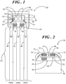
- FIG. 1 shows a front view of a sensor package 20 in accordance with an embodiment and FIG. 2 shows a side view of sensor package 20.
- sensor package 20 may be a speed sensor package for providing rotational speed measurement.
- Sensor package 20 includes a lead frame 22, a sensor component 24, a first capacitor 26, a second capacitor 28 (visible in FIG. 2 ), and a third capacitor 30 located within a housing 32.
- a magnetic element 34 may be attached to an exterior surface 36 of housing 32.
- lead frame 22 includes a sensor mounting area 38, a first lead 40, a second lead 42, and a third lead 44.
- Lead frame 22 (including sensor mounting area 38, first lead 40, second lead 42, and third lead 44) is characterized by a first side 46 and a second side 48 (visible in FIG. 2 ), with second side 48 being parallel and opposite to first side 46.
- Sensor component 24 is attached to first side 46 of sensor mounting area 38.
- first capacitor 26 is interconnected between first and second leads 40, 42, with first capacitor 26 being attached to first side 46 of each of first and second leads 40, 42.
- third capacitor 30 may be interconnected between second and third leads 42, 44, with third capacitor 30 being attached to first side 46 of each of second and third leads 42, 44.
- second capacitor 28 is interconnected between first and second leads 40, 42, with second capacitor 28 being attached to second side 48 (visible in FIG. 2 ) of each of first and second leads 40, 42.
- Sensor package 20 may further include signal processing circuitry 50 associated with sensor component 24.
- sensor component 24 and signal processing circuitry 50 may be combined as an integrated circuit (IC) die 52, with IC die 52 being attached to first side 46 of sensor mounting area 38.
- IC die 52 includes adjacent blocks representing sensor component 24 and signal processing circuitry 50 for simplicity of illustration.
- sensor component 24 may be a magnetic sensor, such as a magnetoresistive sensor.
- the magnetoresistive sensor may be formed of metal layers on top of signal processing circuitry 50 and may be connected to signal processing circuitry 50 by, for example, vias.
- Sensor package 20 may additionally include multiple bond wires 54 interconnected between lead frame 22 and IC die 52.
- bond wires 54 may be coupled to a first terminal element 56 of IC die 52 and to first lead 40. It should be observed that second lead 42 is directly connected to sensor mounting area 38.
- another bond wire 54 may be coupled to a second terminal element 58 of IC die 52 and to second lead 42 via sensor mounting area 38.
- Yet another bond wire 54 may be coupled to a third terminal element 60 of IC die 52 and to third lead 44.
- Housing 32 may be formed from injection-molded epoxy molding compound that fully encapsulates sensor mounting area 38 of lead frame 22, IC die 52, bond wires 54, first, second, and third capacitors 26, 28, 30, and the distal portions of first, second, and third leads 44, 46, 48 at which first, second, and third capacitors 26, 28, 30 are located. Elongated portions 62 of first, second, and third leads 40, 42, 44 extend outside of housing 32. Further, first, second, and third capacitors 26, 28, 30 on first, second, and third leads 40, 42, 44 are proximate, or close to, an entrance location 64 of first, second, and third leads 40, 42, 44 into housing 32.
- first lead 40 is configured to provide power (PWR) to sensor component 24 and signal processing circuitry 50 of IC die 52 via first terminal 56.
- Second lead 42 is configured to be coupled to ground (GND), and
- third lead 44 is configured to provide an output signal (OUT) from sensor component 24 of IC die 52.
- first and second capacitors 26, 28 are in stacked relation with one another at first and second sides 46, 48 of first and second leads 40, 42. That is, first and second capacitors 26, 28 are generally aligned with one another in a double-sided capacitor attach configuration in which the capacitors are placed on both sides of first and second leads 40, 42. However, another capacitor is not interconnected between second and third leads 42, 44 at second side 48 of second and third leads 42, 44.
- capacitors are sometimes implemented in magnetic sensors to serve these functions.
- SiP system-in-package
- sensor component 24 and signal processing circuitry 50 may be integrated into a single IC die 52 to meet stringent size requirements.
- IC die 52 and first, second, and third capacitors 26, 28, 30 may be integrated into a single housing 32 to further minimize size while fulfilling EMC/ESD performance requirements and/or for bridging small interruptions of the power.
- Some capacitance requirements, especially on the input (i.e., first lead 40) are relatively high to protect sensor package 20 and reduce EMC emission. Indeed, better protection may be provided with greater capacitance.
- attachment of large capacitors to the same side of a lead frame as the IC die can be problematic. That is, if the thickness of the capacitors is significantly larger than the thickness of the IC die, the resulting thickness of the side of the molded housing of the sensor package facing a magnetic encoder gear wheel may be undesirably big.
- a large thickness of the side of the molded housing facing a magnetic encoder gear wheel effectively decreases the width of the airgap between the magnetic sense element and the magnetic gear wheel.
- the amount of plastic molding material can have a significant adverse impact on product performance. Accordingly, the thickness of the plastic molded housing between a sensor element and the magnetic gear wheel should be as small as possible. The limited thickness of the plastic molded housing limits the allowed size of the capacitor, and with that, its capacity.
- first and second capacitors 26, 28 are stacked on opposing first and second sides 46, 48 of first and second leads 40, 42 stacked arrangement of first and second capacitors 26, 28 on opposing first and second sides 46, 48 of first and second leads 40, 42 enables the implementation of physically smaller capacitors while still providing sufficiently high capacitance.
- first and second capacitors 26, 28 have a capacitance of one hundred nanofarads (nF)
- the combination of both of first and second capacitors 26, 28 provides two hundred nanofarads of capacitance between first and second leads 40, 42.
- this capacitance can be provided without implementing a capacitor compartment separate from housing 32 that might otherwise hamper folded and/or miniaturization designs. Accordingly, a separate capacitor compartment can be absent from sensor package 20.
- third capacitor 30 may be kept substantially smaller than the combined capacitances of first and second capacitors 26, 28 so as to prevent undesired smoothing of the output pulses.
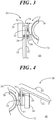
- FIG. 3 shows a side view of sensor package 20 of in a straight sensing configuration 66
- FIG. 4 shows a side view of sensor package 20 in a folded sensing configuration 68.
- Some applications utilize a straight sensing configuration and some applications utilize a folded sensing configuration depending upon how the sensor element is to be located relative to the magnetic target.
- an output signal of sensor component 24 may be a series of output pulses that can be suitably processed by signal processing circuitry 50 ( FIG. 1 ) to yield a speed signal indicative of the movement of gear wheel 70 relative to sensor component 24.
- folded sensing configuration 68 of FIG. 4 elongated portions 62 of leads 40, 42, 44 of lead frame 22 are of a length sufficient to be folded or bent into in folded sensing configuration.
- folded sensing configuration 68 shown in FIG. 4 may be implemented in applications having particular size constraints while still enabling the sensing capability described above in connection with FIG. 3 .
- the double-sided capacitor attach configuration of sensor package 20 enables the same sensor package 20 to be utilized in either of straight or folded sensing configurations 66, 68 without the added complexity of a separate capacitor compartment.
- the straight and folded sensing configurations 66, 68 of FIGs. 3 and 4 show sensor package 20 with magnetic element 34 attached to exterior surface 36 of housing 32 for illustrative purposes.
- alternative embodiments need not include magnetic element 34.
- a sensor package that implements a magnetized target configuration may include the double-sided capacitor attach configuration, like that of sensor package 20, but would not have magnetic element 34.
- the sensor response is not speed, but is an angular position, e.g., the position of a valve throttle.
- An angular magnetic sensor typically utilizes a rotating disk magnet proximate the magnetic sensor in lieu of gear wheel 70.
- an angular magnetic sensor would not include magnetic element 34.
- the double-side attach configuration like that of sensor package 20, may be instrumental in meeting miniaturization and/or increased performance requirements.
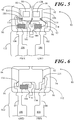
- FIG. 5 shows a front view of a sensor package 80 in accordance with another embodiment and FIG. 6 shows a rear view of sensor package 80.
- Sensor package 80 is provided to illustrate a two lead configuration.
- Sensor package 80 includes a lead frame 82, an IC die 84 combining a sensor component 86 and signal processing circuitry 88, a first capacitor 90, a second capacitor 92, and a third capacitor 94 (visible in FIG. 6 ) located within a housing 96.
- a magnetic element is not shown for simplicity of illustration. However, a magnetic element, such as magnetic element 34 ( FIG. 2 ) may be attached to an exterior surface (i.e., the back side) of housing 96.
- lead frame 82 includes a sensor mounting area 98, a first lead 100, a second lead 102, and a center pin 104 positioned between first and second leads 100, 102.
- Lead frame 82 (including sensor mounting area 98, first lead 100, second lead 102, and center pin 104) is characterized by a first side 106 and a second side 108, with second side 108 being parallel and opposite to first side 106.
- second lead 102 is physically connected to (i.e., extends from) sensor mounting area 98 and sensor mounting area 98 includes an extension region 110 located adjacent to first lead 100.
- IC die 84 is attached to first side 106 of sensor mounting area 98. Additionally, first capacitor 90 is electrically interconnected between first and second leads 100, 102 at first side 106 via extension region 110 and sensor mounting area 98. Second capacitor 92 is electrically interconnected between second lead 102 and center pin 104 at first side 106 of each of second lead 102 and center pin 104. Further, third capacitor 94 is electrically interconnected between second lead 102 and center pin 104 at second side 108 of each of second lead 102 and center pin 104. Thus, second and third capacitors 92, 94 are arranged in stacked relationship on opposing first and second sides 106, 108 of lead frame 82.
- a fourth capacitor 112 may be electrically interconnected between first and second leads 100, 102 at second side 108 via extension region 110 and sensor mounting area 98, as represented by a dashed line rectangle in FIG. 6 . Accordingly, first capacitor 90 and fourth capacitor 112 may be arranged in stacked relationship on opposing first and second sides 106, 108 of lead frame 82.
- Sensor package 80 may additionally include multiple bond wires 114 interconnected between lead frame 82 and IC die 84.
- bond wires 54 may be coupled to a first terminal element 116 of IC die 84 and to first lead 100.
- Another bond wire 114 may be coupled to a second terminal element 118 of IC die 84 and to second lead 102.
- Yet another bond wire 114 may be coupled to a third terminal element 120 of IC die 84 and to center pin 104.
- housing 96 may be formed from injection-molded epoxy molding compound that fully encapsulates sensor mounting area 98 of lead frame 82, IC die 84, bond wires 112, first, second, third, and fourth capacitors 90, 92, 94, 112 and the distal portions of first and second leads 100, 102, and center pin 104. Elongated portions 122 of first and second leads 100, 102 extend outside of housing 96.
- first lead 100 is configured to provide power (PWR) to sensor component 86 and signal processing circuitry 88 of IC die 84 via first terminal element 116.
- Second lead 102 is configured to be coupled to ground (GND).
- speed information sensed via sensor component 86 may be encoded in current pulses on the power supply line, i.e., first lead 100.
- Center pin 104 is not connected to the outside world, but may support second capacitor 92 and third capacitor 94 to stabilize the internal voltage, V INT , for bridging small interruptions of the power.
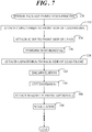
- FIG. 7 shows a flowchart of a sensor package fabrication process 130 in accordance with another embodiment.
- Sensor package fabrication process 130 may be performed to produce either of sensor package 20 ( FIG. 1 ) or sensor package 80 ( FIG. 5 ).
- sensor package fabrication process 130 may be performed to produce these alternative sensor package configurations.
- the following methodology will be described in connection with the fabrication of single sensor package 20.
- FIGs. 1 and 2 should be referred to in conjunction with the following discussion.
- first and third capacitors 26, 30 are attached to the front side, i.e., first side 46, of lead frame 22.
- first capacitor 26 may be bonded to first side 46 of each of first and second leads 40, 42 using, for example, an electrically conductive adhesive, solder, and the like.
- third capacitor 30 may be bonded to first side 46 of each of second and third leads 42, 44 using, for example, the electrically conductive adhesive, solder, and the like.
- IC die 52 may be attached to first side 46 of lead frame 22.
- IC die 52 may be attached to first side 46 of sensor mounting area 38 using, for example, an electrically insulating adhesive.
- a wire bonding process may be performed to form bond wires 54.
- a ball-stitch-on-ball bonding method with silver wire may be performed.
- other processes may be performed to form the electrical interconnects between IC die 52 and lead frame 22.
- second capacitor 28 is attached to the back side, i.e., second side 48 of lead frame 22.
- second capacitor 28 may be attached to second side 48 of each of first and second leads 40, 42 in stacked alignment with first capacitor 26 using, for example, an electrically conductive adhesive, solder, and the like.
- FIG. 8 shows a partial front view of sensor package 20 at an intermediate stage of fabrication in accordance with fabrication process 130.
- back side i.e., second side 48
- first and third capacitors 26, 30 are already attached to the front side (i.e., first side 46).
- first, second, and third capacitors 26, 28, 30 may be positioned closed to the stabilizing dambar 140.
- Dambars typically included on lead frames, are features for plastic molded packages that blocks (i.e., dams) the flow of the plastic molding compound to the external lead area (in this example, elongated portions 62 of first, second, and third leads 40, 42, 44) of the lead frames during molding. Dambars electrically short the leads together and must be removed, i.e., trimmed, before electrically testing the resulting device.
- dambar 140 Prior to back side attachment of second capacitor 28 in accordance with block 138, lead frame 22 should be clamped on dambar 140 to prevent deformation of lead frame 22 during placement and attachment of second capacitor 28.
- housing 32 is formed using a molding compound to encapsulate IC die 52, capacitors 26, 28, 30, sensor mounting area 38 and the distal ends of first, second, third leads 40, 42, 44 of lead frame 22, and wire bonds 54.
- dambars 140 are cut to electrically disconnect leads 40, 42, 44 from one another.
- magnet element 34 is attached to exterior surface 36 of housing 32. Thus, block 146 is shown as an optional operation. Thereafter, a singulation block 148 is performed.
- a plurality of lead frames 22 may be connected to one another and following the aforementioned operations, these lead frames 22 are sawn, diced, or otherwise separated to form a plurality of separate sensor packages 20.
- Operations following singulation block 148 can include device cleaning, testing, packaging, and so forth that are not described herein for brevity.
- An embodiment of a sensor package comprises a lead frame having a sensor mounting area, a first lead, and a second lead, wherein the sensor mounting area, the first lead, and the second lead are characterized by a first side and a second side, the second side being parallel and opposite to the first side.
- a sensor component is attached to the first side of the sensor mounting area, a first capacitor is interconnected between the first and second leads, the first capacitor being attached to the first side of each of the first and second leads, and a second capacitor is interconnected between the first and second leads, the second capacitor being attached to the second side of each of the first and second leads.
- a sensor package comprises a lead frame having a sensor mounting area, a first lead, and a second lead, wherein the sensor mounting area, the first lead, and the second lead are characterized by a first side and a second side, the second side being parallel and opposite to the first side.
- a magnetic sensor component is attached to the first side of the sensor mounting area, a first capacitor interconnected between the first and second leads, the first capacitor being attached to the first side of each of the first and second leads, and a second capacitor is interconnected between the first and second leads, the second capacitor being attached to the second side of each of the first and second leads.
- the sensor package further includes a single housing in which the magnetic sensor component, the first capacitor, and the second capacitor are located.
- An embodiment of a method of forming a sensor package comprises attaching a sensor component to a first side of a sensor mounting area of a lead frame, the lead frame including the sensor mounting area, a first lead, and a second lead, wherein the sensor mounting area, the first lead, and the second lead are characterized by the first side and a second side, the second side being parallel and opposite to the first side.
- the method further comprises attaching a first capacitor to the first side of each of the first and second leads, the first capacitor being interconnected between the first and second leads, attaching a second capacitor to the second side of each of the first and second leads, the second capacitor being interconnected between the first and second leads, and encapsulating the sensor component, the first capacitor, and the second capacitor in a molding compound to form a single housing in which the sensor component, the first capacitor, and the second capacitor are housed.
- the magnetic sensor packages and methodology for fabricating such sensor packages described herein are designed to include a double-sided capacitor attach on the same leads to fulfill electromagnetic compatibility (EMC) and electrostatic discharge (ESD) performance requirements while concurrently meeting size and shape constraints, and enabling usage in "folded applications.”
- EMC electromagnetic compatibility
- ESD electrostatic discharge
Landscapes
- Physics & Mathematics (AREA)
- General Physics & Mathematics (AREA)
- Transmission And Conversion Of Sensor Element Output (AREA)
- Engineering & Computer Science (AREA)
- Power Engineering (AREA)
- Measuring Magnetic Variables (AREA)
Abstract
Description
- The present invention relates generally to sensor packages. More specifically, the present invention relates to a sensor package with a double-sided capacitor attach configuration on the same leads.
- Magnetic sensor systems are increasingly important in a variety of industries. For example, accurate rotational speed measurement is a vital component in maintaining performance, safety, and reliability in modem vehicles. It forms the basis of numerous applications from anti-lock braking to engine management systems, and provides means for embedding intelligence throughout a vehicle via advanced networks and control systems. Accordingly, modem vehicles are increasingly being equipped with magnetic sensors to monitor the speed of a crankshaft or camshaft, to monitor a rotation speed of a wheel about a wheel axis in an anti-lock braking system (ABS), and so forth. Such magnetic sensors (also referred to as speed sensors, angular sensors, and/or rotational sensors) may help increase vehicle stability, reduce vehicle emissions, and enable drive-independent control functions.
- In general, a magnetic speed sensor is configured to sense the motion of a magnetic encoder gear wheel or a magnetized target. A periodic magnetic field stemming from the effect of flux bending by the magnetic gear wheel or directly from the magnetized target is transformed by the magnetic speed sensor into an analog electrical signal. The frequency of the signal is proportional to the rotational speed of the target. Different sensor applications may have different restrictions regarding the size and shape of a sensor package in order to allow the sensor to be mounted as close as necessary to a target to be measured. Additionally, among other design and performance considerations, such magnetic speed sensors are typically required to fulfill electromagnetic compatibility (EMC) and electrostatic discharge (ESD) performance requirements.
- The accompanying figures in which like reference numerals refer to identical or functionally similar elements throughout the separate views, the figures are not necessarily drawn to scale, and which together with the detailed description below are incorporated in and form part of the specification, serve to further illustrate various embodiments and to explain various principles and advantages all in accordance with the present invention.
-
FIG. 1 shows a front view of a sensor package in accordance with an embodiment; -
FIG. 2 shows a side view of the sensor package ofFIG. 1 ; -
FIG. 3 shows a side view of the sensor package ofFIG. 1 in a straight sensing configuration; -
FIG. 4 shows a side view of the sensor package ofFIG. 1 in a folded sensing configuration; -
FIG. 5 shows a front view of a sensor package in accordance with another embodiment; -
FIG. 6 shows a rear view of the sensor package ofFIG. 5 ; -
FIG. 7 shows a flowchart of a sensor package fabrication process in accordance with another embodiment; and -
FIG. 8 shows a partial front view of a sensor package at an intermediate stage of fabrication in accordance with the process ofFIG. 7 . - In overview, the present disclosure concerns magnetic sensor packages and methodology for fabricating such sensor packages. More particularly, a sensor package has a double-sided capacitor attach configuration on the same leads to fulfill electromagnetic compatibility (EMC) and electrostatic discharge (ESD) performance requirements while concurrently meeting size and shape constraints, and enabling usage in "folded applications."
- The instant disclosure is provided to further explain in an enabling fashion the best modes, at the time of the application, of making and using various embodiments in accordance with the present invention. The disclosure is further offered to enhance an understanding and appreciation for the inventive principles and advantages thereof, rather than to limit in any manner the invention. The invention is defined solely by the appended claims including any amendments made during the pendency of this application and all equivalents of those claims as issued.
- It is further understood that the use of relational terms, if any, such as first and second, top and bottom, and the like are used solely to distinguish one from another entity or action without necessarily requiring or implying any actual such relationship or order between such entities or actions. Furthermore, some of the figures may be illustrated using various shading and/or hatching to distinguish the different elements from one another.
- Referring to
FIGs. 1 and 2, FIG. 1 shows a front view of asensor package 20 in accordance with an embodiment andFIG. 2 shows a side view ofsensor package 20. In some embodiments,sensor package 20 may be a speed sensor package for providing rotational speed measurement.Sensor package 20 includes alead frame 22, asensor component 24, afirst capacitor 26, a second capacitor 28 (visible inFIG. 2 ), and athird capacitor 30 located within ahousing 32. In some embodiments, amagnetic element 34 may be attached to anexterior surface 36 ofhousing 32. - In this example,
lead frame 22 includes asensor mounting area 38, afirst lead 40, asecond lead 42, and athird lead 44. Lead frame 22 (includingsensor mounting area 38,first lead 40,second lead 42, and third lead 44) is characterized by afirst side 46 and a second side 48 (visible inFIG. 2 ), withsecond side 48 being parallel and opposite tofirst side 46.Sensor component 24 is attached tofirst side 46 ofsensor mounting area 38. Additionally,first capacitor 26 is interconnected between first and second leads 40, 42, withfirst capacitor 26 being attached tofirst side 46 of each of first and second leads 40, 42. Similarly,third capacitor 30 may be interconnected between second and third leads 42, 44, withthird capacitor 30 being attached tofirst side 46 of each of second and third leads 42, 44. Conversely,second capacitor 28 is interconnected between first and second leads 40, 42, withsecond capacitor 28 being attached to second side 48 (visible inFIG. 2 ) of each of first andsecond leads -
Sensor package 20 may further includesignal processing circuitry 50 associated withsensor component 24. In the illustrated embodiment,sensor component 24 andsignal processing circuitry 50 may be combined as an integrated circuit (IC) die 52, with IC die 52 being attached tofirst side 46 ofsensor mounting area 38. InFIG. 1 , IC die 52 includes adjacent blocks representingsensor component 24 andsignal processing circuitry 50 for simplicity of illustration. However, in an example configuration,sensor component 24 may be a magnetic sensor, such as a magnetoresistive sensor. The magnetoresistive sensor may be formed of metal layers on top ofsignal processing circuitry 50 and may be connected tosignal processing circuitry 50 by, for example, vias. -
Sensor package 20 may additionally includemultiple bond wires 54 interconnected betweenlead frame 22 and IC die 52. For example, one ofbond wires 54 may be coupled to a firstterminal element 56 of IC die 52 and tofirst lead 40. It should be observed thatsecond lead 42 is directly connected tosensor mounting area 38. Thus, anotherbond wire 54 may be coupled to a secondterminal element 58 of IC die 52 and tosecond lead 42 viasensor mounting area 38. Yet anotherbond wire 54 may be coupled to athird terminal element 60 of IC die 52 and tothird lead 44. -
Housing 32 may be formed from injection-molded epoxy molding compound that fully encapsulatessensor mounting area 38 oflead frame 22, IC die 52,bond wires 54, first, second, andthird capacitors third capacitors portions 62 of first, second, and third leads 40, 42, 44 extend outside ofhousing 32. Further, first, second, andthird capacitors entrance location 64 of first, second, and third leads 40, 42, 44 intohousing 32. - In an embodiment,
first lead 40 is configured to provide power (PWR) tosensor component 24 andsignal processing circuitry 50 of IC die 52 viafirst terminal 56.Second lead 42 is configured to be coupled to ground (GND), andthird lead 44 is configured to provide an output signal (OUT) fromsensor component 24 of IC die 52. - As particularly shown in
FIG. 2 , first andsecond capacitors second sides second capacitors second side 48 of second and third leads 42, 44. - For magnetic sensors, such as
sensor package 20, electronic protection elements may be called for in order to fulfill EMC performance requirements, ESD protection, and/or for bridging small interruptions of the power. Capacitors are sometimes implemented in magnetic sensors to serve these functions. Increasingly, system-in-package (SiP) configurations are being utilized to enable a complete functional unit while meeting compact size requirements. Thus,sensor component 24 andsignal processing circuitry 50 may be integrated into a single IC die 52 to meet stringent size requirements. Further, IC die 52 and first, second, andthird capacitors single housing 32 to further minimize size while fulfilling EMC/ESD performance requirements and/or for bridging small interruptions of the power. - Some capacitance requirements, especially on the input (i.e., first lead 40) are relatively high to protect
sensor package 20 and reduce EMC emission. Indeed, better protection may be provided with greater capacitance. Unfortunately, attachment of large capacitors to the same side of a lead frame as the IC die can be problematic. That is, if the thickness of the capacitors is significantly larger than the thickness of the IC die, the resulting thickness of the side of the molded housing of the sensor package facing a magnetic encoder gear wheel may be undesirably big. A large thickness of the side of the molded housing facing a magnetic encoder gear wheel, effectively decreases the width of the airgap between the magnetic sense element and the magnetic gear wheel. The amount of plastic molding material can have a significant adverse impact on product performance. Accordingly, the thickness of the plastic molded housing between a sensor element and the magnetic gear wheel should be as small as possible. The limited thickness of the plastic molded housing limits the allowed size of the capacitor, and with that, its capacity. - The stacked arrangement of first and
second capacitors second sides second capacitors second capacitors housing 32 that might otherwise hamper folded and/or miniaturization designs. Accordingly, a separate capacitor compartment can be absent fromsensor package 20. - As mentioned above, another capacitor may not be not present at
second side 48 oflead frame 22 and interconnecting second and third leads 42, 44 (FIG. 1 ).Third lead 44 provides the output signal as a series of output pulses. The capacitance of third capacitor 30 (FIG. 1 ) may be kept substantially smaller than the combined capacitances of first andsecond capacitors - Referring now to
FIGs. 3 and 4, FIG. 3 shows a side view ofsensor package 20 of in astraight sensing configuration 66, andFIG. 4 shows a side view ofsensor package 20 in a foldedsensing configuration 68. There are various applications in the market for speed sensors and angular sensors. Some applications utilize a straight sensing configuration and some applications utilize a folded sensing configuration depending upon how the sensor element is to be located relative to the magnetic target. - In
straight sensing configuration 66 ofFIG. 3 ,elongated portions 62 ofleads FIG. 1 ) oflead frame 22 are left in an unfolded or straight configuration. Further, IC die 52 faces a magneticencoder gear wheel 70 withsensor component 24 being separated fromgear wheel 70 by anairgap 72 and athickness 74 of the molding compound ofhousing 32.Magnetic element 34 onexterior surface 36 ofhousing 32 is positioned such thatlead frame 22 is interposed between magnetic element andsensor component 24. In this example arrangement, asgear wheel 70 rotates, the teeth ofgear wheel 70 produces periodically recurrent areas that alternately influence a measuring field which is formed by the magnetic field ofmagnet element 34. Accordingly, an output signal ofsensor component 24 may be a series of output pulses that can be suitably processed by signal processing circuitry 50 (FIG. 1 ) to yield a speed signal indicative of the movement ofgear wheel 70 relative tosensor component 24. - In folded
sensing configuration 68 ofFIG. 4 ,elongated portions 62 ofleads lead frame 22 are of a length sufficient to be folded or bent into in folded sensing configuration. Thus, foldedsensing configuration 68 shown inFIG. 4 may be implemented in applications having particular size constraints while still enabling the sensing capability described above in connection withFIG. 3 . Accordingly, the double-sided capacitor attach configuration ofsensor package 20 enables thesame sensor package 20 to be utilized in either of straight or foldedsensing configurations - The straight and folded
sensing configurations FIGs. 3 and 4 show sensor package 20 withmagnetic element 34 attached toexterior surface 36 ofhousing 32 for illustrative purposes. However, alternative embodiments need not includemagnetic element 34. For example, when a magnetized target is utilized in lieu ofgear wheel 70,magnetic element 34 would not be required. Thus, a sensor package that implements a magnetized target configuration may include the double-sided capacitor attach configuration, like that ofsensor package 20, but would not havemagnetic element 34. In an angular magnetic sensor, the sensor response is not speed, but is an angular position, e.g., the position of a valve throttle. An angular magnetic sensor typically utilizes a rotating disk magnet proximate the magnetic sensor in lieu ofgear wheel 70. Thus, an angular magnetic sensor would not includemagnetic element 34. However, in an angular magnetic sensor, the double-side attach configuration, like that ofsensor package 20, may be instrumental in meeting miniaturization and/or increased performance requirements. - Referring to
FIGs. 5 and 6, FIG. 5 shows a front view of asensor package 80 in accordance with another embodiment andFIG. 6 shows a rear view ofsensor package 80.Sensor package 80 is provided to illustrate a two lead configuration.Sensor package 80 includes alead frame 82, an IC die 84 combining asensor component 86 andsignal processing circuitry 88, afirst capacitor 90, asecond capacitor 92, and a third capacitor 94 (visible inFIG. 6 ) located within ahousing 96. A magnetic element is not shown for simplicity of illustration. However, a magnetic element, such as magnetic element 34 (FIG. 2 ) may be attached to an exterior surface (i.e., the back side) ofhousing 96. - In this example,
lead frame 82 includes asensor mounting area 98, afirst lead 100, asecond lead 102, and acenter pin 104 positioned between first andsecond leads sensor mounting area 98,first lead 100,second lead 102, and center pin 104) is characterized by afirst side 106 and asecond side 108, withsecond side 108 being parallel and opposite tofirst side 106. As shown,second lead 102 is physically connected to (i.e., extends from)sensor mounting area 98 andsensor mounting area 98 includes anextension region 110 located adjacent tofirst lead 100. - IC die 84 is attached to
first side 106 ofsensor mounting area 98. Additionally,first capacitor 90 is electrically interconnected between first andsecond leads first side 106 viaextension region 110 andsensor mounting area 98.Second capacitor 92 is electrically interconnected betweensecond lead 102 andcenter pin 104 atfirst side 106 of each ofsecond lead 102 andcenter pin 104. Further,third capacitor 94 is electrically interconnected betweensecond lead 102 andcenter pin 104 atsecond side 108 of each ofsecond lead 102 andcenter pin 104. Thus, second andthird capacitors second sides lead frame 82. - In some embodiments, a
fourth capacitor 112 may be electrically interconnected between first andsecond leads second side 108 viaextension region 110 andsensor mounting area 98, as represented by a dashed line rectangle inFIG. 6 . Accordingly,first capacitor 90 andfourth capacitor 112 may be arranged in stacked relationship on opposing first andsecond sides lead frame 82. -
Sensor package 80 may additionally includemultiple bond wires 114 interconnected betweenlead frame 82 and IC die 84. For example, one ofbond wires 54 may be coupled to a firstterminal element 116 of IC die 84 and tofirst lead 100. Anotherbond wire 114 may be coupled to a secondterminal element 118 of IC die 84 and tosecond lead 102. Yet anotherbond wire 114 may be coupled to a thirdterminal element 120 of IC die 84 and to centerpin 104. - Again,
housing 96 may be formed from injection-molded epoxy molding compound that fully encapsulatessensor mounting area 98 oflead frame 82, IC die 84,bond wires 112, first, second, third, andfourth capacitors second leads center pin 104.Elongated portions 122 of first andsecond leads housing 96. - In an embodiment,
first lead 100 is configured to provide power (PWR) tosensor component 86 andsignal processing circuitry 88 of IC die 84 via firstterminal element 116.Second lead 102 is configured to be coupled to ground (GND). In some embodiments, speed information sensed viasensor component 86 may be encoded in current pulses on the power supply line, i.e.,first lead 100.Center pin 104 is not connected to the outside world, but may supportsecond capacitor 92 andthird capacitor 94 to stabilize the internal voltage, VINT, for bridging small interruptions of the power. -
FIG. 7 shows a flowchart of a sensorpackage fabrication process 130 in accordance with another embodiment. Sensorpackage fabrication process 130 may be performed to produce either of sensor package 20 (FIG. 1 ) or sensor package 80 (FIG. 5 ). However, although two sensor package configurations were described above, it should be understood that alternative sensor package configurations may be envisioned that include the double-sided capacitor attach structure. As such, sensorpackage fabrication process 130 may be performed to produce these alternative sensor package configurations. For simplicity of discussion, the following methodology will be described in connection with the fabrication ofsingle sensor package 20. However, those skilled in the art will readily recognize that multiple sensor packages can be fabricated concurrently.FIGs. 1 and 2 should be referred to in conjunction with the following discussion. - At a
block 132, first andthird capacitors first side 46, oflead frame 22. In particular,first capacitor 26 may be bonded tofirst side 46 of each of first and second leads 40, 42 using, for example, an electrically conductive adhesive, solder, and the like. Likewise,third capacitor 30 may be bonded tofirst side 46 of each of second and third leads 42, 44 using, for example, the electrically conductive adhesive, solder, and the like. At ablock 134, IC die 52 may be attached tofirst side 46 oflead frame 22. In particular, IC die 52 may be attached tofirst side 46 ofsensor mounting area 38 using, for example, an electrically insulating adhesive. At ablock 136, a wire bonding process may be performed to formbond wires 54. By way of example, a ball-stitch-on-ball bonding method with silver wire may be performed. However, other processes may be performed to form the electrical interconnects between IC die 52 andlead frame 22. - At a
block 138,second capacitor 28 is attached to the back side, i.e.,second side 48 oflead frame 22. For example,second capacitor 28 may be attached tosecond side 48 of each of first and second leads 40, 42 in stacked alignment withfirst capacitor 26 using, for example, an electrically conductive adhesive, solder, and the like. - Referring to
FIG. 8 in connection withblock 138,FIG. 8 shows a partial front view ofsensor package 20 at an intermediate stage of fabrication in accordance withfabrication process 130. During back side (i.e., second side 48) attachment ofsecond capacitor 28, the distal ends of first, second, and third leads 40, 42, 44 may not be fully supported since first andthird capacitors third capacitors dambar 140. Dambars, typically included on lead frames, are features for plastic molded packages that blocks (i.e., dams) the flow of the plastic molding compound to the external lead area (in this example,elongated portions 62 of first, second, and third leads 40, 42, 44) of the lead frames during molding. Dambars electrically short the leads together and must be removed, i.e., trimmed, before electrically testing the resulting device. Prior to back side attachment ofsecond capacitor 28 in accordance withblock 138,lead frame 22 should be clamped ondambar 140 to prevent deformation oflead frame 22 during placement and attachment ofsecond capacitor 28. - Returning to sensor
package fabrication process 130, following back side attachment ofsecond capacitor 28, encapsulation is performed at ablock 142. Atblock 142,housing 32 is formed using a molding compound to encapsulate IC die 52,capacitors sensor mounting area 38 and the distal ends of first, second, third leads 40, 42, 44 oflead frame 22, andwire bonds 54. At ablock 144,dambars 140 are cut to electrically disconnect leads 40, 42, 44 from one another. At ablock 146, for a magnetic sensor package calling for an external magnet,magnet element 34 is attached toexterior surface 36 ofhousing 32. Thus, block 146 is shown as an optional operation. Thereafter, asingulation block 148 is performed. That is, a plurality of lead frames 22 may be connected to one another and following the aforementioned operations, these lead frames 22 are sawn, diced, or otherwise separated to form a plurality of separate sensor packages 20. Operations followingsingulation block 148 can include device cleaning, testing, packaging, and so forth that are not described herein for brevity. - Thus, sensor packages having a double-sided attach configuration are disclosed herein. An embodiment of a sensor package comprises a lead frame having a sensor mounting area, a first lead, and a second lead, wherein the sensor mounting area, the first lead, and the second lead are characterized by a first side and a second side, the second side being parallel and opposite to the first side. A sensor component is attached to the first side of the sensor mounting area, a first capacitor is interconnected between the first and second leads, the first capacitor being attached to the first side of each of the first and second leads, and a second capacitor is interconnected between the first and second leads, the second capacitor being attached to the second side of each of the first and second leads.
- Another embodiment of a sensor package comprises a lead frame having a sensor mounting area, a first lead, and a second lead, wherein the sensor mounting area, the first lead, and the second lead are characterized by a first side and a second side, the second side being parallel and opposite to the first side. A magnetic sensor component is attached to the first side of the sensor mounting area, a first capacitor interconnected between the first and second leads, the first capacitor being attached to the first side of each of the first and second leads, and a second capacitor is interconnected between the first and second leads, the second capacitor being attached to the second side of each of the first and second leads. The sensor package further includes a single housing in which the magnetic sensor component, the first capacitor, and the second capacitor are located.
- An embodiment of a method of forming a sensor package comprises attaching a sensor component to a first side of a sensor mounting area of a lead frame, the lead frame including the sensor mounting area, a first lead, and a second lead, wherein the sensor mounting area, the first lead, and the second lead are characterized by the first side and a second side, the second side being parallel and opposite to the first side. The method further comprises attaching a first capacitor to the first side of each of the first and second leads, the first capacitor being interconnected between the first and second leads, attaching a second capacitor to the second side of each of the first and second leads, the second capacitor being interconnected between the first and second leads, and encapsulating the sensor component, the first capacitor, and the second capacitor in a molding compound to form a single housing in which the sensor component, the first capacitor, and the second capacitor are housed.
- The magnetic sensor packages and methodology for fabricating such sensor packages described herein are designed to include a double-sided capacitor attach on the same leads to fulfill electromagnetic compatibility (EMC) and electrostatic discharge (ESD) performance requirements while concurrently meeting size and shape constraints, and enabling usage in "folded applications."
- This disclosure is intended to explain how to fashion and use various embodiments in accordance with the invention rather than to limit the true, intended, and fair scope and spirit thereof. The foregoing description is not intended to be exhaustive or to limit the invention to the precise form disclosed. Modifications or variations are possible in light of the above teachings. The embodiment(s) was chosen and described to provide the best illustration of the principles of the invention and its practical application, and to enable one of ordinary skill in the art to utilize the invention in various embodiments and with various modifications as are suited to the particular use contemplated. All such modifications and variations are within the scope of the invention as determined by the appended claims, as may be amended during the pendency of this application for patent, and all equivalents thereof, when interpreted in accordance with the breadth to which they are fairly, legally, and equitably entitled.
Claims (15)
- A sensor package comprising:a lead frame (22, 82) having a sensor mounting area (28, 98), a first lead (40, 100), and a second lead (42, 102), wherein said sensor mounting area (28, 98), said first lead (40, 100), and said second lead (42, 102) are characterized by a first side (46, 106) and a second side (48, 108), said second side (48, 108) being parallel and opposite to said first side (46, 106);a sensor component (24, 86) attached to said first side (46, 106) of said sensor mounting area (28, 98);a first capacitor (26, 90) interconnected between said first and second leads (40, 100; 42, 102), said first capacitor (26, 90) being attached to said first side (46, 106) of each of said first and second leads (40, 100; 42, 102); anda second capacitor (28, 92) interconnected between said first and second leads, said second capacitor (28, 92) being attached to said second side (48, 108) of said each of said first and second leads (40, 100; 42, 102).
- The sensor package of claim 1, further comprising signal processing circuitry (50, 88) associated with said sensor component (24, 86), wherein said sensor component (24, 86) and said signal processing circuitry (50, 88) are combined as an integrated circuit die (52, 84), and said integrated circuit die (52, 84) is attached to said first side (46, 106) of said sensor mounting area (28, 98).
- The sensor package of claim 1 or claim 2, wherein said first lead (40, 100) is configured to provide power to said sensor component (24, 86) and said second lead (42, 102) is configured to be coupled to ground.
- The sensor package of claim 3, wherein said lead frame (22, 82) further comprises a third lead (44), said third lead (44) being configured to provide an output signal from said sensor component (24, 86), and wherein a capacitor is not interconnected between said second and third leads (42, 102; 44) at said second side (48, 108) of each of said second and third leads (42, 102; 44).
- The sensor package of any one of the claims 1 to 4, wherein said first and second capacitors (26, 90; 28, 92) are in stacked relation with one another at said first and second sides (46, 106; 48, 108) of said first and second leads (40, 100; 42, 102).
- The sensor package of any one of the claims 1 to 5, further comprising a single housing (32, 96) in which said sensor component (24, 86), said first capacitor (26, 90), and said second capacitor (28, 92) are located.
- The sensor package of claim 6, wherein said housing (32, 96) is formed from a molding compound.
- The sensor package of claim 6 or claim 7, wherein said first and second leads (40, 100; 42, 102) extend outside of said housing (32, 96) and said second capacitor (28, 92) is positioned at said second side (48, 108) of said each of said first and second leads (40, 100; 42, 102) proximate an entrance location (64) of said first and second leads (40, 100; 42, 102) into said housing (32, 96).
- The sensor package of any one of the claims 6 to 8, further comprising a magnetic element (34) attached to an exterior surface (36) of said housing (32, 96), wherein following attachment of said magnetic element (34) to said exterior surface, said lead frame (22, 82) is interposed between said magnetic element (34) and said sensor component (24, 86).
- The sensor package of any one of the claims 6 to 9, wherein a capacitor compartment that is separate from said housing (32, 96) is absent from said sensor package.
- The sensor package of any one of the claims 6 to 10, wherein elongated portions (62, 122) of said first and second leads (40, 100; 42, 102) extend outside of said housing (32, 96), and said elongated portions (62, 122) are of a length sufficient to be placed in a folded configuration (68).
- The sensor package of any one of the claims 1 to 11, wherein said sensor component (24, 86) comprises a magnetic sensor component (70).
- The sensor package of any one of the claims 1 to 12, wherein said sensor package comprises a speed sensor package.
- A method of forming a sensor package comprising:attaching a sensor component (24, 86) to a first side (46, 106) of a sensor mounting area (28, 98) of a lead frame (22, 82), said lead frame (22, 82) including said sensor mounting area (28, 98), a first lead (40, 100), and a second lead (42, 102), wherein said sensor mounting area (28, 98), said first lead (40, 100), and said second lead (42, 102) are characterized by said first side (46, 106) and a second side (48, 108), said second side (48, 108) being parallel and opposite to said first side (46, 106);attaching a first capacitor (26, 90) to said first side (46, 106) of each of said first and second leads (40, 100; 42, 102), said first capacitor (26, 90) being interconnected between said first and second leads (40, 100; 42, 102);attaching a second capacitor (28, 92) to said second side (48, 108) of said each of said first and second leads (40, 100; 42, 102), said second capacitor (28, 92) being interconnected between said first and second leads (40, 100; 42, 102); andencapsulating said sensor component (24, 86), said first capacitor (26, 90), and said second capacitor (28, 92) in a molding compound to form a single housing (32, 96) in which said sensor component (24, 86), said first capacitor (26, 90), and said second capacitor (28, 92) are housed.
- The method of claim 14, wherein said attaching said second capacitor (28, 92) comprises positioning said second capacitor (28, 92) at said second side (48, 108) of said each of said first and second leads (40, 100; 42, 102) such that said second capacitor (28, 92) is proximate an entrance location (64) of said first and second leads (40, 100; 42, 102) into said housing (32, 96) following said encapsulating operation.
Applications Claiming Priority (1)
| Application Number | Priority Date | Filing Date | Title |
|---|---|---|---|
| US15/334,063 US9958292B1 (en) | 2016-10-25 | 2016-10-25 | Sensor package with double-sided capacitor attach on same leads and method of fabrication |
Publications (2)
| Publication Number | Publication Date |
|---|---|
| EP3315921A1 true EP3315921A1 (en) | 2018-05-02 |
| EP3315921B1 EP3315921B1 (en) | 2020-04-01 |
Family
ID=60161933
Family Applications (1)
| Application Number | Title | Priority Date | Filing Date |
|---|---|---|---|
| EP17195819.2A Active EP3315921B1 (en) | 2016-10-25 | 2017-10-10 | Sensor package with double-sided capacitor attach on same leads and method of fabrication |
Country Status (2)
| Country | Link |
|---|---|
| US (1) | US9958292B1 (en) |
| EP (1) | EP3315921B1 (en) |
Families Citing this family (6)
| Publication number | Priority date | Publication date | Assignee | Title |
|---|---|---|---|---|
| EP3544394A1 (en) * | 2018-03-24 | 2019-09-25 | Melexis Technologies SA | Integrated circuit lead frame design and method |
| US10354943B1 (en) | 2018-07-12 | 2019-07-16 | Infineon Technologies Ag | Multi-branch terminal for integrated circuit (IC) package |
| DE102018217658A1 (en) * | 2018-10-15 | 2020-04-16 | Continental Automotive Gmbh | GMR or TMR sensor in use with a ferromagnetic encoder |
| DE102019110570B4 (en) * | 2019-04-24 | 2023-05-25 | Infineon Technologies Ag | MAGNETIC FIELD SENSOR PACKAGE WITH INTEGRATED PASSIVE COMPONENT |
| CN110794160A (en) * | 2019-08-29 | 2020-02-14 | 天生桥二级水力发电有限公司天生桥水力发电总厂 | Proximity switch distance-adjusting module of large hydroelectric generating set speed measuring device |
| US20240334604A1 (en) * | 2023-03-27 | 2024-10-03 | Honeywell Federal Manufacturing & Technologies, Llc | Method for locating hall effect sensor assembly |
Citations (4)
| Publication number | Priority date | Publication date | Assignee | Title |
|---|---|---|---|---|
| US20130249544A1 (en) * | 2012-03-20 | 2013-09-26 | Allegro Microsystems, Inc. | Magnetic Field Sensor Integrated Circuit with Integral Ferromagnetic Material |
| US20130249546A1 (en) * | 2012-03-20 | 2013-09-26 | Allegro Microsystems, Llc | Integrated circuit package having a split lead frame |
| US20130249027A1 (en) * | 2012-03-20 | 2013-09-26 | Allegro Microsystems, Inc. | Integrated circuit package having a split lead frame |
| US20130249029A1 (en) * | 2012-03-20 | 2013-09-26 | Allegro Microsystems, Llc | Magnetic Field Sensor Integrated Circuit with Integral Ferromagnetic Material |
Family Cites Families (10)
| Publication number | Priority date | Publication date | Assignee | Title |
|---|---|---|---|---|
| EP1031038A1 (en) | 1998-06-22 | 2000-08-30 | Koninklijke Philips Electronics N.V. | Magnetic position detector |
| DE10118819A1 (en) | 2001-04-17 | 2002-10-24 | Philips Corp Intellectual Pty | Arrangement for determining the position of a motion sensor element |
| EP1706747B1 (en) | 2004-01-08 | 2013-11-20 | Nxp B.V. | Magnetoresistive speed sensor |
| US7378721B2 (en) | 2005-12-05 | 2008-05-27 | Honeywell International Inc. | Chip on lead frame for small package speed sensor |
| US20080013298A1 (en) * | 2006-07-14 | 2008-01-17 | Nirmal Sharma | Methods and apparatus for passive attachment of components for integrated circuits |
| DE102008064046A1 (en) | 2008-10-02 | 2010-04-08 | Continental Teves Ag & Co. Ohg | Method for producing a speed sensor element |
| DE102009054521A1 (en) | 2009-07-28 | 2011-02-03 | Continental Teves Ag & Co. Ohg | Speed sensor |
| US8969978B2 (en) * | 2012-04-27 | 2015-03-03 | Melexis Technologies Nv | TMAP sensor systems and methods for manufacturing those |
| DE102014118769B4 (en) * | 2014-12-16 | 2017-11-23 | Infineon Technologies Ag | Pressure sensor module with a sensor chip and passive components within a common housing |
| EP3156770A1 (en) * | 2015-10-15 | 2017-04-19 | Nxp B.V. | Rotational sensor |
-
2016
- 2016-10-25 US US15/334,063 patent/US9958292B1/en active Active
-
2017
- 2017-10-10 EP EP17195819.2A patent/EP3315921B1/en active Active
Patent Citations (4)
| Publication number | Priority date | Publication date | Assignee | Title |
|---|---|---|---|---|
| US20130249544A1 (en) * | 2012-03-20 | 2013-09-26 | Allegro Microsystems, Inc. | Magnetic Field Sensor Integrated Circuit with Integral Ferromagnetic Material |
| US20130249546A1 (en) * | 2012-03-20 | 2013-09-26 | Allegro Microsystems, Llc | Integrated circuit package having a split lead frame |
| US20130249027A1 (en) * | 2012-03-20 | 2013-09-26 | Allegro Microsystems, Inc. | Integrated circuit package having a split lead frame |
| US20130249029A1 (en) * | 2012-03-20 | 2013-09-26 | Allegro Microsystems, Llc | Magnetic Field Sensor Integrated Circuit with Integral Ferromagnetic Material |
Also Published As
| Publication number | Publication date |
|---|---|
| US9958292B1 (en) | 2018-05-01 |
| US20180113001A1 (en) | 2018-04-26 |
| EP3315921B1 (en) | 2020-04-01 |
Similar Documents
| Publication | Publication Date | Title |
|---|---|---|
| EP3315921B1 (en) | Sensor package with double-sided capacitor attach on same leads and method of fabrication | |
| EP2783229B1 (en) | Magnetic field sensor device having non-conductive die paddle and production method | |
| JP6336576B2 (en) | Integrated circuit package having split lead frame and magnet | |
| JP6462907B2 (en) | Sensor | |
| JP6335159B2 (en) | Integrated circuit package with split leadframe | |
| CN103090890B (en) | Magnetic sensor device | |
| WO1999019735A1 (en) | Packaged integrated circuit with magnetic flux concentrator | |
| US10607925B2 (en) | Integrated circuit package having a raised lead edge | |
| KR20150053238A (en) | Micromechanical sensor device | |
| JPH06140451A (en) | Semiconductor integrated circuit device | |
| US20210057314A1 (en) | Integrated circuit package having a low profile | |
| CN111863788B (en) | Magnetic field sensor package with integrated passive components | |
| CN212387732U (en) | Electronic device | |
| CN114899169A (en) | Multi-chip flat-laying packaging structure | |
| CN217641313U (en) | Single chip packaging structure | |
| JP2001091613A (en) | Multi-chip module for magnetic sensor | |
| CN115101501A (en) | Single chip packaging structure | |
| CN114927507A (en) | Multi-chip stacking and packaging structure |
Legal Events
| Date | Code | Title | Description |
|---|---|---|---|
| PUAI | Public reference made under article 153(3) epc to a published international application that has entered the european phase |
Free format text: ORIGINAL CODE: 0009012 |
|
| STAA | Information on the status of an ep patent application or granted ep patent |
Free format text: STATUS: THE APPLICATION HAS BEEN PUBLISHED |
|
| AK | Designated contracting states |
Kind code of ref document: A1 Designated state(s): AL AT BE BG CH CY CZ DE DK EE ES FI FR GB GR HR HU IE IS IT LI LT LU LV MC MK MT NL NO PL PT RO RS SE SI SK SM TR |
|
| AX | Request for extension of the european patent |
Extension state: BA ME |
|
| STAA | Information on the status of an ep patent application or granted ep patent |
Free format text: STATUS: REQUEST FOR EXAMINATION WAS MADE |
|
| 17P | Request for examination filed |
Effective date: 20181102 |
|
| RBV | Designated contracting states (corrected) |
Designated state(s): AL AT BE BG CH CY CZ DE DK EE ES FI FR GB GR HR HU IE IS IT LI LT LU LV MC MK MT NL NO PL PT RO RS SE SI SK SM TR |
|
| GRAP | Despatch of communication of intention to grant a patent |
Free format text: ORIGINAL CODE: EPIDOSNIGR1 |
|
| STAA | Information on the status of an ep patent application or granted ep patent |
Free format text: STATUS: GRANT OF PATENT IS INTENDED |
|
| RIC1 | Information provided on ipc code assigned before grant |
Ipc: G01D 11/24 20060101AFI20191016BHEP Ipc: H01L 49/02 20060101ALI20191016BHEP |
|
| INTG | Intention to grant announced |
Effective date: 20191115 |
|
| GRAS | Grant fee paid |
Free format text: ORIGINAL CODE: EPIDOSNIGR3 |
|
| GRAA | (expected) grant |
Free format text: ORIGINAL CODE: 0009210 |
|
| STAA | Information on the status of an ep patent application or granted ep patent |
Free format text: STATUS: THE PATENT HAS BEEN GRANTED |
|
| AK | Designated contracting states |
Kind code of ref document: B1 Designated state(s): AL AT BE BG CH CY CZ DE DK EE ES FI FR GB GR HR HU IE IS IT LI LT LU LV MC MK MT NL NO PL PT RO RS SE SI SK SM TR |
|
| REG | Reference to a national code |
Ref country code: GB Ref legal event code: FG4D |
|
| REG | Reference to a national code |
Ref country code: CH Ref legal event code: EP Ref country code: AT Ref legal event code: REF Ref document number: 1251939 Country of ref document: AT Kind code of ref document: T Effective date: 20200415 |
|
| REG | Reference to a national code |
Ref country code: DE Ref legal event code: R096 Ref document number: 602017013902 Country of ref document: DE |
|
| REG | Reference to a national code |
Ref country code: IE Ref legal event code: FG4D |
|
| PG25 | Lapsed in a contracting state [announced via postgrant information from national office to epo] |
Ref country code: BG Free format text: LAPSE BECAUSE OF FAILURE TO SUBMIT A TRANSLATION OF THE DESCRIPTION OR TO PAY THE FEE WITHIN THE PRESCRIBED TIME-LIMIT Effective date: 20200701 |
|
| REG | Reference to a national code |
Ref country code: NL Ref legal event code: MP Effective date: 20200401 |
|
| REG | Reference to a national code |
Ref country code: LT Ref legal event code: MG4D |
|
| PG25 | Lapsed in a contracting state [announced via postgrant information from national office to epo] |
Ref country code: CZ Free format text: LAPSE BECAUSE OF FAILURE TO SUBMIT A TRANSLATION OF THE DESCRIPTION OR TO PAY THE FEE WITHIN THE PRESCRIBED TIME-LIMIT Effective date: 20200401 Ref country code: NL Free format text: LAPSE BECAUSE OF FAILURE TO SUBMIT A TRANSLATION OF THE DESCRIPTION OR TO PAY THE FEE WITHIN THE PRESCRIBED TIME-LIMIT Effective date: 20200401 Ref country code: FI Free format text: LAPSE BECAUSE OF FAILURE TO SUBMIT A TRANSLATION OF THE DESCRIPTION OR TO PAY THE FEE WITHIN THE PRESCRIBED TIME-LIMIT Effective date: 20200401 Ref country code: NO Free format text: LAPSE BECAUSE OF FAILURE TO SUBMIT A TRANSLATION OF THE DESCRIPTION OR TO PAY THE FEE WITHIN THE PRESCRIBED TIME-LIMIT Effective date: 20200701 Ref country code: GR Free format text: LAPSE BECAUSE OF FAILURE TO SUBMIT A TRANSLATION OF THE DESCRIPTION OR TO PAY THE FEE WITHIN THE PRESCRIBED TIME-LIMIT Effective date: 20200702 Ref country code: PT Free format text: LAPSE BECAUSE OF FAILURE TO SUBMIT A TRANSLATION OF THE DESCRIPTION OR TO PAY THE FEE WITHIN THE PRESCRIBED TIME-LIMIT Effective date: 20200817 Ref country code: LT Free format text: LAPSE BECAUSE OF FAILURE TO SUBMIT A TRANSLATION OF THE DESCRIPTION OR TO PAY THE FEE WITHIN THE PRESCRIBED TIME-LIMIT Effective date: 20200401 Ref country code: IS Free format text: LAPSE BECAUSE OF FAILURE TO SUBMIT A TRANSLATION OF THE DESCRIPTION OR TO PAY THE FEE WITHIN THE PRESCRIBED TIME-LIMIT Effective date: 20200801 Ref country code: SE Free format text: LAPSE BECAUSE OF FAILURE TO SUBMIT A TRANSLATION OF THE DESCRIPTION OR TO PAY THE FEE WITHIN THE PRESCRIBED TIME-LIMIT Effective date: 20200401 |
|
| REG | Reference to a national code |
Ref country code: AT Ref legal event code: MK05 Ref document number: 1251939 Country of ref document: AT Kind code of ref document: T Effective date: 20200401 |
|
| PG25 | Lapsed in a contracting state [announced via postgrant information from national office to epo] |
Ref country code: RS Free format text: LAPSE BECAUSE OF FAILURE TO SUBMIT A TRANSLATION OF THE DESCRIPTION OR TO PAY THE FEE WITHIN THE PRESCRIBED TIME-LIMIT Effective date: 20200401 Ref country code: HR Free format text: LAPSE BECAUSE OF FAILURE TO SUBMIT A TRANSLATION OF THE DESCRIPTION OR TO PAY THE FEE WITHIN THE PRESCRIBED TIME-LIMIT Effective date: 20200401 Ref country code: LV Free format text: LAPSE BECAUSE OF FAILURE TO SUBMIT A TRANSLATION OF THE DESCRIPTION OR TO PAY THE FEE WITHIN THE PRESCRIBED TIME-LIMIT Effective date: 20200401 |
|
| PG25 | Lapsed in a contracting state [announced via postgrant information from national office to epo] |
Ref country code: AL Free format text: LAPSE BECAUSE OF FAILURE TO SUBMIT A TRANSLATION OF THE DESCRIPTION OR TO PAY THE FEE WITHIN THE PRESCRIBED TIME-LIMIT Effective date: 20200401 |
|
| REG | Reference to a national code |
Ref country code: DE Ref legal event code: R097 Ref document number: 602017013902 Country of ref document: DE |
|
| PG25 | Lapsed in a contracting state [announced via postgrant information from national office to epo] |
Ref country code: IT Free format text: LAPSE BECAUSE OF FAILURE TO SUBMIT A TRANSLATION OF THE DESCRIPTION OR TO PAY THE FEE WITHIN THE PRESCRIBED TIME-LIMIT Effective date: 20200401 Ref country code: SM Free format text: LAPSE BECAUSE OF FAILURE TO SUBMIT A TRANSLATION OF THE DESCRIPTION OR TO PAY THE FEE WITHIN THE PRESCRIBED TIME-LIMIT Effective date: 20200401 Ref country code: AT Free format text: LAPSE BECAUSE OF FAILURE TO SUBMIT A TRANSLATION OF THE DESCRIPTION OR TO PAY THE FEE WITHIN THE PRESCRIBED TIME-LIMIT Effective date: 20200401 Ref country code: EE Free format text: LAPSE BECAUSE OF FAILURE TO SUBMIT A TRANSLATION OF THE DESCRIPTION OR TO PAY THE FEE WITHIN THE PRESCRIBED TIME-LIMIT Effective date: 20200401 Ref country code: RO Free format text: LAPSE BECAUSE OF FAILURE TO SUBMIT A TRANSLATION OF THE DESCRIPTION OR TO PAY THE FEE WITHIN THE PRESCRIBED TIME-LIMIT Effective date: 20200401 Ref country code: ES Free format text: LAPSE BECAUSE OF FAILURE TO SUBMIT A TRANSLATION OF THE DESCRIPTION OR TO PAY THE FEE WITHIN THE PRESCRIBED TIME-LIMIT Effective date: 20200401 Ref country code: DK Free format text: LAPSE BECAUSE OF FAILURE TO SUBMIT A TRANSLATION OF THE DESCRIPTION OR TO PAY THE FEE WITHIN THE PRESCRIBED TIME-LIMIT Effective date: 20200401 |
|
| PLBE | No opposition filed within time limit |
Free format text: ORIGINAL CODE: 0009261 |
|
| STAA | Information on the status of an ep patent application or granted ep patent |
Free format text: STATUS: NO OPPOSITION FILED WITHIN TIME LIMIT |
|
| PG25 | Lapsed in a contracting state [announced via postgrant information from national office to epo] |
Ref country code: PL Free format text: LAPSE BECAUSE OF FAILURE TO SUBMIT A TRANSLATION OF THE DESCRIPTION OR TO PAY THE FEE WITHIN THE PRESCRIBED TIME-LIMIT Effective date: 20200401 Ref country code: SK Free format text: LAPSE BECAUSE OF FAILURE TO SUBMIT A TRANSLATION OF THE DESCRIPTION OR TO PAY THE FEE WITHIN THE PRESCRIBED TIME-LIMIT Effective date: 20200401 |
|
| 26N | No opposition filed |
Effective date: 20210112 |
|
| PG25 | Lapsed in a contracting state [announced via postgrant information from national office to epo] |
Ref country code: SI Free format text: LAPSE BECAUSE OF FAILURE TO SUBMIT A TRANSLATION OF THE DESCRIPTION OR TO PAY THE FEE WITHIN THE PRESCRIBED TIME-LIMIT Effective date: 20200401 |
|
| REG | Reference to a national code |
Ref country code: CH Ref legal event code: PL |
|
| PG25 | Lapsed in a contracting state [announced via postgrant information from national office to epo] |
Ref country code: LU Free format text: LAPSE BECAUSE OF NON-PAYMENT OF DUE FEES Effective date: 20201010 Ref country code: MC Free format text: LAPSE BECAUSE OF FAILURE TO SUBMIT A TRANSLATION OF THE DESCRIPTION OR TO PAY THE FEE WITHIN THE PRESCRIBED TIME-LIMIT Effective date: 20200401 |
|
| REG | Reference to a national code |
Ref country code: BE Ref legal event code: MM Effective date: 20201031 |
|
| PG25 | Lapsed in a contracting state [announced via postgrant information from national office to epo] |
Ref country code: FR Free format text: LAPSE BECAUSE OF NON-PAYMENT OF DUE FEES Effective date: 20201031 |
|
| PG25 | Lapsed in a contracting state [announced via postgrant information from national office to epo] |
Ref country code: LI Free format text: LAPSE BECAUSE OF NON-PAYMENT OF DUE FEES Effective date: 20201031 Ref country code: CH Free format text: LAPSE BECAUSE OF NON-PAYMENT OF DUE FEES Effective date: 20201031 Ref country code: BE Free format text: LAPSE BECAUSE OF NON-PAYMENT OF DUE FEES Effective date: 20201031 |
|
| PG25 | Lapsed in a contracting state [announced via postgrant information from national office to epo] |
Ref country code: IE Free format text: LAPSE BECAUSE OF NON-PAYMENT OF DUE FEES Effective date: 20201010 |
|
| PG25 | Lapsed in a contracting state [announced via postgrant information from national office to epo] |
Ref country code: TR Free format text: LAPSE BECAUSE OF FAILURE TO SUBMIT A TRANSLATION OF THE DESCRIPTION OR TO PAY THE FEE WITHIN THE PRESCRIBED TIME-LIMIT Effective date: 20200401 Ref country code: MT Free format text: LAPSE BECAUSE OF FAILURE TO SUBMIT A TRANSLATION OF THE DESCRIPTION OR TO PAY THE FEE WITHIN THE PRESCRIBED TIME-LIMIT Effective date: 20200401 Ref country code: CY Free format text: LAPSE BECAUSE OF FAILURE TO SUBMIT A TRANSLATION OF THE DESCRIPTION OR TO PAY THE FEE WITHIN THE PRESCRIBED TIME-LIMIT Effective date: 20200401 |
|
| GBPC | Gb: european patent ceased through non-payment of renewal fee |
Effective date: 20211010 |
|
| PG25 | Lapsed in a contracting state [announced via postgrant information from national office to epo] |
Ref country code: MK Free format text: LAPSE BECAUSE OF FAILURE TO SUBMIT A TRANSLATION OF THE DESCRIPTION OR TO PAY THE FEE WITHIN THE PRESCRIBED TIME-LIMIT Effective date: 20200401 |
|
| PG25 | Lapsed in a contracting state [announced via postgrant information from national office to epo] |
Ref country code: GB Free format text: LAPSE BECAUSE OF NON-PAYMENT OF DUE FEES Effective date: 20211010 |
|
| P01 | Opt-out of the competence of the unified patent court (upc) registered |
Effective date: 20230725 |
|
| PGFP | Annual fee paid to national office [announced via postgrant information from national office to epo] |
Ref country code: DE Payment date: 20250923 Year of fee payment: 9 |